EP4024831A1 - Bildschirmanordnung einer elektronischen vorrichtung und elektronische vorrichtung - Google Patents
Bildschirmanordnung einer elektronischen vorrichtung und elektronische vorrichtung Download PDFInfo
- Publication number
- EP4024831A1 EP4024831A1 EP20876802.8A EP20876802A EP4024831A1 EP 4024831 A1 EP4024831 A1 EP 4024831A1 EP 20876802 A EP20876802 A EP 20876802A EP 4024831 A1 EP4024831 A1 EP 4024831A1
- Authority
- EP
- European Patent Office
- Prior art keywords
- light
- hole
- camera
- electronic device
- ring edge
- Prior art date
- Legal status (The legal status is an assumption and is not a legal conclusion. Google has not performed a legal analysis and makes no representation as to the accuracy of the status listed.)
- Withdrawn
Links
Images




Classifications
-
- H—ELECTRICITY
- H04—ELECTRIC COMMUNICATION TECHNIQUE
- H04M—TELEPHONIC COMMUNICATION
- H04M1/00—Substation equipment, e.g. for use by subscribers
- H04M1/02—Constructional features of telephone sets
- H04M1/0202—Portable telephone sets, e.g. cordless phones, mobile phones or bar type handsets
- H04M1/026—Details of the structure or mounting of specific components
- H04M1/0264—Details of the structure or mounting of specific components for a camera module assembly
-
- G—PHYSICS
- G06—COMPUTING OR CALCULATING; COUNTING
- G06F—ELECTRIC DIGITAL DATA PROCESSING
- G06F1/00—Details not covered by groups G06F3/00 - G06F13/00 and G06F21/00
- G06F1/16—Constructional details or arrangements
- G06F1/1613—Constructional details or arrangements for portable computers
- G06F1/1633—Constructional details or arrangements of portable computers not specific to the type of enclosures covered by groups G06F1/1615 - G06F1/1626
- G06F1/1637—Details related to the display arrangement, including those related to the mounting of the display in the housing
-
- G—PHYSICS
- G02—OPTICS
- G02B—OPTICAL ELEMENTS, SYSTEMS OR APPARATUS
- G02B5/00—Optical elements other than lenses
- G02B5/30—Polarising elements
- G02B5/3025—Polarisers, i.e. arrangements capable of producing a definite output polarisation state from an unpolarised input state
- G02B5/3033—Polarisers, i.e. arrangements capable of producing a definite output polarisation state from an unpolarised input state in the form of a thin sheet or foil, e.g. Polaroid
-
- G—PHYSICS
- G06—COMPUTING OR CALCULATING; COUNTING
- G06F—ELECTRIC DIGITAL DATA PROCESSING
- G06F1/00—Details not covered by groups G06F3/00 - G06F13/00 and G06F21/00
- G06F1/16—Constructional details or arrangements
- G06F1/1613—Constructional details or arrangements for portable computers
- G06F1/1626—Constructional details or arrangements for portable computers with a single-body enclosure integrating a flat display, e.g. Personal Digital Assistants [PDAs]
-
- G—PHYSICS
- G06—COMPUTING OR CALCULATING; COUNTING
- G06F—ELECTRIC DIGITAL DATA PROCESSING
- G06F1/00—Details not covered by groups G06F3/00 - G06F13/00 and G06F21/00
- G06F1/16—Constructional details or arrangements
- G06F1/1613—Constructional details or arrangements for portable computers
- G06F1/1633—Constructional details or arrangements of portable computers not specific to the type of enclosures covered by groups G06F1/1615 - G06F1/1626
- G06F1/1684—Constructional details or arrangements related to integrated I/O peripherals not covered by groups G06F1/1635 - G06F1/1675
- G06F1/1686—Constructional details or arrangements related to integrated I/O peripherals not covered by groups G06F1/1635 - G06F1/1675 the I/O peripheral being an integrated camera
-
- H—ELECTRICITY
- H04—ELECTRIC COMMUNICATION TECHNIQUE
- H04M—TELEPHONIC COMMUNICATION
- H04M1/00—Substation equipment, e.g. for use by subscribers
- H04M1/02—Constructional features of telephone sets
- H04M1/0202—Portable telephone sets, e.g. cordless phones, mobile phones or bar type handsets
- H04M1/026—Details of the structure or mounting of specific components
-
- H—ELECTRICITY
- H04—ELECTRIC COMMUNICATION TECHNIQUE
- H04N—PICTORIAL COMMUNICATION, e.g. TELEVISION
- H04N23/00—Cameras or camera modules comprising electronic image sensors; Control thereof
- H04N23/50—Constructional details
- H04N23/51—Housings
-
- H—ELECTRICITY
- H04—ELECTRIC COMMUNICATION TECHNIQUE
- H04N—PICTORIAL COMMUNICATION, e.g. TELEVISION
- H04N23/00—Cameras or camera modules comprising electronic image sensors; Control thereof
- H04N23/57—Mechanical or electrical details of cameras or camera modules specially adapted for being embedded in other devices
-
- H—ELECTRICITY
- H04—ELECTRIC COMMUNICATION TECHNIQUE
- H04M—TELEPHONIC COMMUNICATION
- H04M1/00—Substation equipment, e.g. for use by subscribers
- H04M1/02—Constructional features of telephone sets
- H04M1/0202—Portable telephone sets, e.g. cordless phones, mobile phones or bar type handsets
- H04M1/026—Details of the structure or mounting of specific components
- H04M1/0266—Details of the structure or mounting of specific components for a display module assembly
-
- H—ELECTRICITY
- H04—ELECTRIC COMMUNICATION TECHNIQUE
- H04M—TELEPHONIC COMMUNICATION
- H04M1/00—Substation equipment, e.g. for use by subscribers
- H04M1/02—Constructional features of telephone sets
- H04M1/0202—Portable telephone sets, e.g. cordless phones, mobile phones or bar type handsets
- H04M1/0279—Improving the user comfort or ergonomics
- H04M1/0283—Improving the user comfort or ergonomics for providing a decorative aspect, e.g. customization of casings, exchangeable faceplate
-
- H—ELECTRICITY
- H10—SEMICONDUCTOR DEVICES; ELECTRIC SOLID-STATE DEVICES NOT OTHERWISE PROVIDED FOR
- H10K—ORGANIC ELECTRIC SOLID-STATE DEVICES
- H10K59/00—Integrated devices, or assemblies of multiple devices, comprising at least one organic light-emitting element covered by group H10K50/00
- H10K59/10—OLED displays
- H10K59/12—Active-matrix OLED [AMOLED] displays
- H10K59/131—Interconnections, e.g. wiring lines or terminals
Definitions
- the present disclosure relates to the field of communication devices technologies, and in particular, to a screen assembly of an electronic device, and an electronic device.
- the "Hole-notched Screen” is to define a through hole or blind hole on the screen, compared with the "Bangs-notched Screen", defining a hole on the screen is more conducive to increase the screen display area, i.e., the "screen-to-body ratio", to provide a more stunning display effect.
- the existence of the hole leads to lack of display at the hole. Especially when the hole is large, the display effect of the screen is adversely affected.
- the present disclosure provides a screen assembly of an electronic device.
- the screen assembly of the electronic device has the advantages of simple structure and good visual effects.
- the present disclosure provides a screen assembly of an electronic device, comprising: a camera; a display assembly, comprising a cover, an optical adhesive layer, a polarizer, an upper glass, a lower glass, and a foam layer stacked in order from a top to a bottom; wherein the polarizer defines a first light through hole, and the foam layer defines a second light through hole, the first light through hole facing the second light through hole; the camera is arranged under the display assembly; and a circular wiring area, arranged on an upper surface of the upper glass and comprising an inner ring edge and an outer ring edge; wherein an inner wall of the first light through hole is arranged at a radially outer side of the inner ring edge; wherein light is suitable for passing from the cover, the optical adhesive layer, the first light through hole, an inner ring area defined by the inner ring edge, the upper glass, the lower glass, and the second light through hole, and being transmitted to the camera.
- the inner wall of the first light through hole is arranged on the radially outer side of the inner ring edge of the circular wiring area.
- a blind hole structure is formed at the position where the display assembly is facing the camera.
- the inner wall of the first light through hole is arranged on the radially outer side of the inner ring edge, which can expose a partial structure of the circular wiring area to form a silver edge area.
- the design of the silver edge area can take advantage of visual differences to reduce the area on the display assembly facing the camera and not displaying images, thereby improving the display effect of the screen assembly.
- the present disclosure further provides an electronic device, comprising: a housing; a camera; a display assembly, embedded in the housing and comprising a cover, an optical adhesive layer, a polarizer, an upper glass, a lower glass, and a foam layer stacked in order from a top to a bottom; wherein the polarizer defines a first light through hole, and the foam layer defines a second light through hole, the first light through hole facing the second light through hole; the camera is arranged in the housing and under the display assembly; and a circular wiring area, arranged on an upper surface of the upper glass and comprising an inner ring edge and an outer ring edge; wherein an inner wall of the first light through hole is arranged at a radially outer side of the inner ring edge; wherein light is suitable for passing from the cover, the optical adhesive layer, the first light through hole, an inner ring area defined by the inner ring edge, the upper glass, the lower glass, and the second light through hole, and being transmitted to the camera.
- the inner wall of the first light through hole is arranged on the radially outer side of the inner ring edge of the circular wiring area.
- a blind hole structure is formed at the position where the display assembly is facing the camera.
- the inner wall of the first light through hole is arranged on the radially outer side of the inner ring edge, which can expose a partial structure of the circular wiring area to form a silver edge area.
- the design of the silver edge area can take advantage of visual differences to reduce the area on the display assembly facing the camera and not displaying images, thereby improving the display effect of the screen assembly.
- orientation or positional relationships indicated by terms “center”, “upper”, “lower”, “front”, “rear”, “left”, “right”, “vertical”, “horizontal”, “top”, “bottom”, “inner”, “outer”, etc. are based on the orientation or positional relationships shown in the accompanying drawings and are intended only to facilitate and simplify the description of the present disclosure, and are not intended to indicate or imply that the device or element referred to must have a particular orientation, be constructed and operate in a particular orientation, and therefore are not to be construed as limiting the present disclosure.
- first and second are only intended for descriptive purposes, and cannot be understood as indicating or implying relative importance or implicitly indicating the number of indicated technical features. Thus, the features defined with “first” and “second” may explicitly or implicitly include one or more of these features. Further, in the description of the present disclosure, unless otherwise specified, “plurality” means two or more.
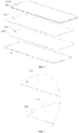
- the screen assembly 102 of the electronic device includes a camera 110 and a display assembly 120.
- the display assembly 120 may include a cover 121, an optical adhesive layer 1211, a polarizer 122, an upper glass 123, a lower glass 124, and a foam layer 125 stacked in order from top to bottom.
- the optical adhesive layer 1211 may be configured to bond the cover 121 and the polarizer 122 together. That is, the cover 121 and the polarizer 122 are bonded together, and an adhesive structure between the cover 121 and the polarizer 122 may be the optical adhesive layer 1211.
- the optical adhesive layer 1211 may be formed by curing glue with a light-transmitting effect.
- the polarizer 122 defines a first light through hole 1221
- the foam layer 125 defines a second light through hole 1251.
- the first light through hole 1221 faces the second light through hole 1251.
- the camera 110 is arranged under the display assembly 120. Further, a light inlet 111 of the camera 110 is defined under the display assembly 120.
- an optical axis of the camera 110 is parallel to an axis of the first light through hole 1221 and an axis of the second light through hole 1251.
- the optical axis of the camera 110 is collinear with the axis of the first light through hole 1221 and the axis of the second light through hole 1251.
- the screen assembly 102 may have a full-screen structure, that is, a full-screen structure with an under-screen camera 110 may be realized.
- the display assembly 120 may be an OLED display screen.
- the OLED display screen may include the cover 121, the optical adhesive layer 1211, the polarizer 122, the upper glass 123, the lower glass 124, and the foam layer 125.
- the cover 121 may be a glass cover and configured to protect components under the cover 121.
- the OLED display screen has a wiring area inside, and metal wires in the wiring area may supply power to the OLED display screen to perform a display function.
- the wiring area may be arranged in a ring structure, that is, the wiring area of the OLED display screen may include a circular wiring area 130.
- the display assembly 120 has an area 103 facing the camera 110 and not displaying images, the circular wiring area 130 is an opaque area, and the circular wiring area 130 may surround an outer periphery of the area 103.
- the area 103 on the display assembly facing the camera and not displaying images may be circular.
- the shape of the area 103 on the display assembly facing the camera and not displaying images is not specifically limited.
- the area 103 on the display assembly facing the camera and not displaying images may be an oblong circle.
- the circular wiring area 130 is arranged on an upper surface of the upper glass 123.
- the circular wiring area 130 includes an inner ring edge 131 and an outer ring edge 132.
- An inner wall of the first light through hole 1221 is arranged at a radially outer side of the inner ring edge 131.
- Light is suitable for passing from the cover 121, the optical adhesive layer 1211, the first light through hole 1221, an inner ring area defined by the inner ring edge 131, the upper glass 123, the lower glass 124, and the second light through hole 1251 and being transmitted to the camera 110.
- the inner wall of the first light through hole 1221 is arranged on the radially outer side of the inner ring edge 131 of the circular wiring area 130.
- a blind hole structure is formed at the position where the display assembly 120 is facing the camera 110.
- the inner wall of the first light through hole 1221 is arranged on the radially outer side of the inner ring edge 131, which can expose a partial structure of the circular wiring area to form a silver edge area 141.
- the design of the silver edge area 141 can take advantage of visual differences to reduce the area 103 on the display assembly 120 facing the camera 110 and not displaying images, thereby improving the display effect of the screen assembly 102.
- a distance between the inner wall of the first light through hole 1221 and the inner ring edge 131 is L1.
- the inner wall of the first light through hole 1221 is arranged at the radially inner side of the outer ring edge 132. In other words, the inner wall of the first light through hole 1221 is located between the outer ring edge 132 and the inner ring edge 131.
- a distance between the inner ring edge 131 and the outer ring edge 132 is L2, where L2 is 0.4-0.5 mm.
- a lower surface of the upper glass 123 may define a groove 1231, the groove 1231 facing the second light through hole 1251.
- the electronic device 100 includes the housing 101, the camera 110, the display assembly 120 and the circular wiring area 130.
- the display assembly 120 is embedded in the housing 101.
- the display assembly 120 includes the cover 121, the optical adhesive layer 1211, the polarizer 122, the upper glass 123, the lower glass 124, and the foam layer 125 stacked from top to bottom.
- the polarizer 122 defines the first light through hole 1221
- the foam layer 125 defines the second light through hole 1251, the first light through hole 1221 facing the second light through hole 1251.
- the camera 110 is arranged in the housing 101 and under the display assembly 120. As shown in FIG. 8 and FIG. 9 , the camera 110 is arranged under the display assembly 120. Further, the light inlet 111 of the camera 110 is defined under the display assembly 120.
- an optical axis of the camera 110 is parallel to an axis of the first light through hole 1221 and an axis of the second light through hole 1251.
- the optical axis of the camera 110 is collinear with the axis of the first light through hole 1221 and the axis of the second light through hole 1251.
- the screen assembly 102 may have a full-screen structure, that is, a full-screen structure with an under-screen camera 110 may be realized.
- the display assembly 120 may be an OLED display screen.
- the OLED display screen may include the cover 121, the optical adhesive layer 1211, the polarizer 122, the upper glass 123, the lower glass 124, and the foam layer 125.
- the OLED display screen has a wiring area inside, and metal wires in the wiring area may supply power to the OLED display screen to perform a display function.
- the wiring area may be arranged in a ring structure, that is, the wiring area of the OLED display screen may include the circular wiring area 130.
- the display assembly 120 has an area 103 facing the camera 110 and not displaying images, the circular wiring area 130 is an opaque area, and the circular wiring area 130 may surround an outer periphery of the area 103.
- the circular wiring area 130 is arranged on an upper surface of the upper glass 123.
- the circular wiring area 130 includes an inner ring edge 131 and an outer ring edge 132.
- An inner wall of the first light through hole 1221 is arranged at a radially outer side of the inner ring edge 131.
- Light is suitable for passing from the cover 121, the optical adhesive layer 1211, the first light through hole 1221, an inner ring area defined by the inner ring edge 131, the upper glass 123, the lower glass 124, and the second light through hole 1251 and being transmitted to the camera 110.
- the camera 110 may be arranged in the housing 101 through a bracket 112, and the camera 110 may be electrically connected to a main board 104 of the electronic device 100 through the flexible circuit board 114, and a connecting seat 113 arranged on the flexible circuit board 114, such that the light information collected by the camera 110 may be transmitted to the main board 104
- the inner wall of the first light through hole 1221 is arranged on the radially outer side of the inner ring edge 131 of the circular wiring area 130.
- a blind hole structure is formed at the position where the display assembly 120 is facing the camera 110.
- the inner wall of the first light through hole 1221 is arranged on the radially outer side of the inner ring edge 131, which can expose a partial structure of the circular wiring area to form a silver edge area 141.
- the design of the silver edge area 141 can take advantage of visual differences to reduce the area 103 on the display assembly 120 facing the camera 110 and not displaying images, thereby improving the display effect of the screen assembly 102.
- a distance between the inner wall of the first light through hole 1221 and the inner ring edge 131 is L1.
- the inner wall of the first light through hole 1221 is arranged at the radially inner side of the outer ring edge 132. In other words, the inner wall of the first light through hole 1221 is located between the outer ring edge 132 and the inner ring edge 131.
- a distance between the inner ring edge 131 and the outer ring edge 132 is L2, where L2 is 0.4-0.5 mm.
- a lower surface of the upper glass 123 may define a groove 1231, the groove 1231 facing the second light through hole 1251.
- orientation or positional relationships indicated by terms “center”, “length”, “upper”, “lower”, “horizontal”, “inner”, “outer”, “axial”, “radial”, “circumferential”, etc. are based on the orientation or position relationships shown in the accompanying drawings, and are only for the convenience of describing the present disclosure and simplifying the description, rather than indicating or implying that the device or element referred to must have a particular orientation, be constructed and operate in a particular orientation, and therefore are not to be construed as limiting the present disclosure.
- “plurality” means two or more.
Landscapes
- Engineering & Computer Science (AREA)
- Theoretical Computer Science (AREA)
- Computer Hardware Design (AREA)
- Physics & Mathematics (AREA)
- General Physics & Mathematics (AREA)
- Signal Processing (AREA)
- Human Computer Interaction (AREA)
- General Engineering & Computer Science (AREA)
- Multimedia (AREA)
- Optics & Photonics (AREA)
- Studio Devices (AREA)
Applications Claiming Priority (2)
| Application Number | Priority Date | Filing Date | Title |
|---|---|---|---|
| CN201910983586.0A CN110769095B (zh) | 2019-10-16 | 2019-10-16 | 电子设备的屏幕组件及电子设备 |
| PCT/CN2020/116890 WO2021073374A1 (zh) | 2019-10-16 | 2020-09-22 | 电子设备的屏幕组件及电子设备 |
Publications (2)
| Publication Number | Publication Date |
|---|---|
| EP4024831A1 true EP4024831A1 (de) | 2022-07-06 |
| EP4024831A4 EP4024831A4 (de) | 2022-11-23 |
Family
ID=69332494
Family Applications (1)
| Application Number | Title | Priority Date | Filing Date |
|---|---|---|---|
| EP20876802.8A Withdrawn EP4024831A4 (de) | 2019-10-16 | 2020-09-22 | Bildschirmanordnung einer elektronischen vorrichtung und elektronische vorrichtung |
Country Status (4)
| Country | Link |
|---|---|
| US (1) | US20220197339A1 (de) |
| EP (1) | EP4024831A4 (de) |
| CN (1) | CN110769095B (de) |
| WO (1) | WO2021073374A1 (de) |
Families Citing this family (6)
| Publication number | Priority date | Publication date | Assignee | Title |
|---|---|---|---|---|
| CN110769095B (zh) * | 2019-10-16 | 2022-05-20 | Oppo广东移动通信有限公司 | 电子设备的屏幕组件及电子设备 |
| CN110867136B (zh) * | 2019-11-22 | 2021-10-15 | 维沃移动通信有限公司 | 极点屏及电子设备 |
| CN111432101B (zh) * | 2020-03-30 | 2021-09-10 | 维沃移动通信有限公司 | 电子设备 |
| CN114740552B (zh) * | 2022-04-20 | 2023-05-30 | 武汉华星光电半导体显示技术有限公司 | 显示模组及显示装置 |
| KR20240042286A (ko) * | 2022-09-23 | 2024-04-02 | 삼성디스플레이 주식회사 | 표시 장치 및 이의 제조방법 |
| CN119094876B (zh) * | 2024-08-08 | 2025-04-04 | 华为技术有限公司 | 马达组件及其组装方法、摄像模组及电子设备 |
Family Cites Families (8)
| Publication number | Priority date | Publication date | Assignee | Title |
|---|---|---|---|---|
| US10191577B2 (en) * | 2016-02-16 | 2019-01-29 | Samsung Electronics Co., Ltd. | Electronic device |
| CN107395928A (zh) * | 2017-08-01 | 2017-11-24 | 维沃移动通信有限公司 | 一种光学组件及移动终端 |
| CN108989508B (zh) * | 2018-08-24 | 2021-03-26 | Oppo(重庆)智能科技有限公司 | 一种显示屏组装方法、显示屏及电子设备 |
| CN208862900U (zh) * | 2018-09-28 | 2019-05-14 | 维沃移动通信有限公司 | 一种显示面板和终端设备 |
| CN208672989U (zh) * | 2018-09-29 | 2019-03-29 | Oppo广东移动通信有限公司 | 显示屏组件及具有其的电子装置 |
| CN209388081U (zh) * | 2019-03-27 | 2019-09-13 | 信利光电股份有限公司 | 一种显示装置 |
| CN110769095B (zh) * | 2019-10-16 | 2022-05-20 | Oppo广东移动通信有限公司 | 电子设备的屏幕组件及电子设备 |
| CN110728905B (zh) * | 2019-11-18 | 2021-01-26 | 维沃移动通信有限公司 | 电子设备 |
-
2019
- 2019-10-16 CN CN201910983586.0A patent/CN110769095B/zh active Active
-
2020
- 2020-09-22 WO PCT/CN2020/116890 patent/WO2021073374A1/zh not_active Ceased
- 2020-09-22 EP EP20876802.8A patent/EP4024831A4/de not_active Withdrawn
-
2022
- 2022-03-10 US US17/691,773 patent/US20220197339A1/en not_active Abandoned
Also Published As
| Publication number | Publication date |
|---|---|
| WO2021073374A1 (zh) | 2021-04-22 |
| CN110769095A (zh) | 2020-02-07 |
| CN110769095B (zh) | 2022-05-20 |
| EP4024831A4 (de) | 2022-11-23 |
| US20220197339A1 (en) | 2022-06-23 |
Similar Documents
| Publication | Publication Date | Title |
|---|---|---|
| EP4024831A1 (de) | Bildschirmanordnung einer elektronischen vorrichtung und elektronische vorrichtung | |
| JP6862553B2 (ja) | 表示パネルを備えた電子機器 | |
| EP3490233B1 (de) | Näherungssensor teilweise hinter dem touch-screen | |
| CN110164297B (zh) | 显示屏模组及其制作方法、偏光片和电子设备 | |
| EP4021155A1 (de) | Dekorationsanordnung, gehäuseanordnung und elektronische vorrichtung | |
| CN113746958B (zh) | 电子设备及电子设备的装配方法 | |
| CN106843398A (zh) | 电子装置 | |
| WO2018205804A1 (zh) | 输入输出模组及电子装置 | |
| CN113451361A (zh) | 显示装置 | |
| CN107911507A (zh) | 显示屏组件及电子设备 | |
| EP3816727B1 (de) | Bildschirmmodul und elektronische vorrichtung | |
| CN113760050B (zh) | 电子设备的屏幕组件及电子设备 | |
| JP2020027282A (ja) | レンズモジュール | |
| CN110867136B (zh) | 极点屏及电子设备 | |
| CN211349378U (zh) | 屏下指纹识别装置及电子设备 | |
| CN113099005A (zh) | 电子设备 | |
| CN209964153U (zh) | 电子设备 | |
| CN105100307B (zh) | 一种移动终端芯片补强板的固定结构及移动终端 | |
| CN207853948U (zh) | 电子设备 | |
| CN110740201B (zh) | 电子设备的屏幕组件及电子设备 | |
| WO2021068853A1 (zh) | 一种电子设备 | |
| CN116723381B (zh) | 一种摄像模组及电子设备 | |
| CN107948421A (zh) | 显示屏及电子设备 | |
| US11588086B2 (en) | Micro-LED display | |
| CN117201650A (zh) | 一种移动终端 |
Legal Events
| Date | Code | Title | Description |
|---|---|---|---|
| STAA | Information on the status of an ep patent application or granted ep patent |
Free format text: STATUS: THE INTERNATIONAL PUBLICATION HAS BEEN MADE |
|
| PUAI | Public reference made under article 153(3) epc to a published international application that has entered the european phase |
Free format text: ORIGINAL CODE: 0009012 |
|
| STAA | Information on the status of an ep patent application or granted ep patent |
Free format text: STATUS: REQUEST FOR EXAMINATION WAS MADE |
|
| 17P | Request for examination filed |
Effective date: 20220331 |
|
| AK | Designated contracting states |
Kind code of ref document: A1 Designated state(s): AL AT BE BG CH CY CZ DE DK EE ES FI FR GB GR HR HU IE IS IT LI LT LU LV MC MK MT NL NO PL PT RO RS SE SI SK SM TR |
|
| A4 | Supplementary search report drawn up and despatched |
Effective date: 20221020 |
|
| RIC1 | Information provided on ipc code assigned before grant |
Ipc: G06F 1/16 20060101ALI20221014BHEP Ipc: H04N 5/225 20060101ALI20221014BHEP Ipc: H04M 1/02 20060101AFI20221014BHEP |
|
| DAV | Request for validation of the european patent (deleted) | ||
| DAX | Request for extension of the european patent (deleted) | ||
| STAA | Information on the status of an ep patent application or granted ep patent |
Free format text: STATUS: EXAMINATION IS IN PROGRESS |
|
| 17Q | First examination report despatched |
Effective date: 20231220 |
|
| STAA | Information on the status of an ep patent application or granted ep patent |
Free format text: STATUS: THE APPLICATION HAS BEEN WITHDRAWN |
|
| 18W | Application withdrawn |
Effective date: 20240123 |