EP4024449A1 - Semiconductor structure and fabrication method therefor - Google Patents
Semiconductor structure and fabrication method therefor Download PDFInfo
- Publication number
- EP4024449A1 EP4024449A1 EP21865320.2A EP21865320A EP4024449A1 EP 4024449 A1 EP4024449 A1 EP 4024449A1 EP 21865320 A EP21865320 A EP 21865320A EP 4024449 A1 EP4024449 A1 EP 4024449A1
- Authority
- EP
- European Patent Office
- Prior art keywords
- structures
- dielectric layer
- conductive pillar
- connecting structure
- semiconductor structure
- Prior art date
- Legal status (The legal status is an assumption and is not a legal conclusion. Google has not performed a legal analysis and makes no representation as to the accuracy of the status listed.)
- Granted
Links
Images





Classifications
-
- H—ELECTRICITY
- H10—SEMICONDUCTOR DEVICES; ELECTRIC SOLID-STATE DEVICES NOT OTHERWISE PROVIDED FOR
- H10W—GENERIC PACKAGES, INTERCONNECTIONS, CONNECTORS OR OTHER CONSTRUCTIONAL DETAILS OF DEVICES COVERED BY CLASS H10
- H10W20/00—Interconnections in chips, wafers or substrates
- H10W20/20—Interconnections within wafers or substrates, e.g. through-silicon vias [TSV]
-
- H—ELECTRICITY
- H10—SEMICONDUCTOR DEVICES; ELECTRIC SOLID-STATE DEVICES NOT OTHERWISE PROVIDED FOR
- H10W—GENERIC PACKAGES, INTERCONNECTIONS, CONNECTORS OR OTHER CONSTRUCTIONAL DETAILS OF DEVICES COVERED BY CLASS H10
- H10W20/00—Interconnections in chips, wafers or substrates
- H10W20/01—Manufacture or treatment
- H10W20/021—Manufacture or treatment of interconnections within wafers or substrates
- H10W20/023—Manufacture or treatment of interconnections within wafers or substrates the interconnections being through-semiconductor vias
-
- H—ELECTRICITY
- H10—SEMICONDUCTOR DEVICES; ELECTRIC SOLID-STATE DEVICES NOT OTHERWISE PROVIDED FOR
- H10W—GENERIC PACKAGES, INTERCONNECTIONS, CONNECTORS OR OTHER CONSTRUCTIONAL DETAILS OF DEVICES COVERED BY CLASS H10
- H10W20/00—Interconnections in chips, wafers or substrates
- H10W20/01—Manufacture or treatment
- H10W20/021—Manufacture or treatment of interconnections within wafers or substrates
- H10W20/023—Manufacture or treatment of interconnections within wafers or substrates the interconnections being through-semiconductor vias
- H10W20/0234—Manufacture or treatment of interconnections within wafers or substrates the interconnections being through-semiconductor vias comprising etching via holes that stop on pads or on electrodes
-
- H—ELECTRICITY
- H10—SEMICONDUCTOR DEVICES; ELECTRIC SOLID-STATE DEVICES NOT OTHERWISE PROVIDED FOR
- H10W—GENERIC PACKAGES, INTERCONNECTIONS, CONNECTORS OR OTHER CONSTRUCTIONAL DETAILS OF DEVICES COVERED BY CLASS H10
- H10W20/00—Interconnections in chips, wafers or substrates
- H10W20/01—Manufacture or treatment
- H10W20/021—Manufacture or treatment of interconnections within wafers or substrates
- H10W20/023—Manufacture or treatment of interconnections within wafers or substrates the interconnections being through-semiconductor vias
- H10W20/0242—Manufacture or treatment of interconnections within wafers or substrates the interconnections being through-semiconductor vias comprising etching via holes from the back sides of the chips, wafers or substrates
-
- H—ELECTRICITY
- H10—SEMICONDUCTOR DEVICES; ELECTRIC SOLID-STATE DEVICES NOT OTHERWISE PROVIDED FOR
- H10W—GENERIC PACKAGES, INTERCONNECTIONS, CONNECTORS OR OTHER CONSTRUCTIONAL DETAILS OF DEVICES COVERED BY CLASS H10
- H10W20/00—Interconnections in chips, wafers or substrates
- H10W20/01—Manufacture or treatment
- H10W20/021—Manufacture or treatment of interconnections within wafers or substrates
- H10W20/023—Manufacture or treatment of interconnections within wafers or substrates the interconnections being through-semiconductor vias
- H10W20/0245—Manufacture or treatment of interconnections within wafers or substrates the interconnections being through-semiconductor vias comprising use of blind vias during the manufacture
-
- H—ELECTRICITY
- H10—SEMICONDUCTOR DEVICES; ELECTRIC SOLID-STATE DEVICES NOT OTHERWISE PROVIDED FOR
- H10W—GENERIC PACKAGES, INTERCONNECTIONS, CONNECTORS OR OTHER CONSTRUCTIONAL DETAILS OF DEVICES COVERED BY CLASS H10
- H10W20/00—Interconnections in chips, wafers or substrates
- H10W20/01—Manufacture or treatment
- H10W20/031—Manufacture or treatment of conductive parts of the interconnections
-
- H—ELECTRICITY
- H10—SEMICONDUCTOR DEVICES; ELECTRIC SOLID-STATE DEVICES NOT OTHERWISE PROVIDED FOR
- H10W—GENERIC PACKAGES, INTERCONNECTIONS, CONNECTORS OR OTHER CONSTRUCTIONAL DETAILS OF DEVICES COVERED BY CLASS H10
- H10W20/00—Interconnections in chips, wafers or substrates
- H10W20/01—Manufacture or treatment
- H10W20/031—Manufacture or treatment of conductive parts of the interconnections
- H10W20/056—Manufacture or treatment of conductive parts of the interconnections by filling conductive material into holes, grooves or trenches
-
- H—ELECTRICITY
- H10—SEMICONDUCTOR DEVICES; ELECTRIC SOLID-STATE DEVICES NOT OTHERWISE PROVIDED FOR
- H10W—GENERIC PACKAGES, INTERCONNECTIONS, CONNECTORS OR OTHER CONSTRUCTIONAL DETAILS OF DEVICES COVERED BY CLASS H10
- H10W20/00—Interconnections in chips, wafers or substrates
- H10W20/40—Interconnections external to wafers or substrates, e.g. back-end-of-line [BEOL] metallisations or vias connecting to gate electrodes
- H10W20/41—Interconnections external to wafers or substrates, e.g. back-end-of-line [BEOL] metallisations or vias connecting to gate electrodes characterised by their conductive parts
- H10W20/42—Vias, e.g. via plugs
-
- H—ELECTRICITY
- H10—SEMICONDUCTOR DEVICES; ELECTRIC SOLID-STATE DEVICES NOT OTHERWISE PROVIDED FOR
- H10W—GENERIC PACKAGES, INTERCONNECTIONS, CONNECTORS OR OTHER CONSTRUCTIONAL DETAILS OF DEVICES COVERED BY CLASS H10
- H10W70/00—Package substrates; Interposers; Redistribution layers [RDL]
- H10W70/60—Insulating or insulated package substrates; Interposers; Redistribution layers
- H10W70/611—Insulating or insulated package substrates; Interposers; Redistribution layers for connecting multiple chips together
-
- H—ELECTRICITY
- H10—SEMICONDUCTOR DEVICES; ELECTRIC SOLID-STATE DEVICES NOT OTHERWISE PROVIDED FOR
- H10W—GENERIC PACKAGES, INTERCONNECTIONS, CONNECTORS OR OTHER CONSTRUCTIONAL DETAILS OF DEVICES COVERED BY CLASS H10
- H10W70/00—Package substrates; Interposers; Redistribution layers [RDL]
- H10W70/60—Insulating or insulated package substrates; Interposers; Redistribution layers
- H10W70/62—Insulating or insulated package substrates; Interposers; Redistribution layers characterised by their interconnections
- H10W70/65—Shapes or dispositions of interconnections
-
- H—ELECTRICITY
- H10—SEMICONDUCTOR DEVICES; ELECTRIC SOLID-STATE DEVICES NOT OTHERWISE PROVIDED FOR
- H10W—GENERIC PACKAGES, INTERCONNECTIONS, CONNECTORS OR OTHER CONSTRUCTIONAL DETAILS OF DEVICES COVERED BY CLASS H10
- H10W20/00—Interconnections in chips, wafers or substrates
- H10W20/40—Interconnections external to wafers or substrates, e.g. back-end-of-line [BEOL] metallisations or vias connecting to gate electrodes
-
- H—ELECTRICITY
- H10—SEMICONDUCTOR DEVICES; ELECTRIC SOLID-STATE DEVICES NOT OTHERWISE PROVIDED FOR
- H10W—GENERIC PACKAGES, INTERCONNECTIONS, CONNECTORS OR OTHER CONSTRUCTIONAL DETAILS OF DEVICES COVERED BY CLASS H10
- H10W20/00—Interconnections in chips, wafers or substrates
- H10W20/40—Interconnections external to wafers or substrates, e.g. back-end-of-line [BEOL] metallisations or vias connecting to gate electrodes
- H10W20/41—Interconnections external to wafers or substrates, e.g. back-end-of-line [BEOL] metallisations or vias connecting to gate electrodes characterised by their conductive parts
- H10W20/43—Layouts of interconnections
-
- H—ELECTRICITY
- H10—SEMICONDUCTOR DEVICES; ELECTRIC SOLID-STATE DEVICES NOT OTHERWISE PROVIDED FOR
- H10W—GENERIC PACKAGES, INTERCONNECTIONS, CONNECTORS OR OTHER CONSTRUCTIONAL DETAILS OF DEVICES COVERED BY CLASS H10
- H10W70/00—Package substrates; Interposers; Redistribution layers [RDL]
- H10W70/60—Insulating or insulated package substrates; Interposers; Redistribution layers
- H10W70/62—Insulating or insulated package substrates; Interposers; Redistribution layers characterised by their interconnections
- H10W70/63—Vias, e.g. via plugs
- H10W70/635—Through-vias
Definitions
- the embodiments of the disclosure relate, but are not limited to a semiconductor structure and a method for manufacturing the same.
- Interconnection between chips or wafers in a semiconductor structure may be implemented through manufacturing via holes in a perpendicular direction, and the interconnection technology is called as a Through Silicon Via (TSV) technology.
- TSV Through Silicon Via
- the traditional TSV is usually filled with a metal material to form a conductive pillar, and an end surface of the conductive pillar is in contact and electric connection with another electrical connection layer to implement electric connection among different layers.
- the embodiments of the disclosure provide a semiconductor structure.
- the semiconductor structure includes a base, a conductive pillar at least located in the base, connecting structures and an electrical connection layer. At least one connecting structure is electrically connected to an end of the conductive pillar, the material of the connecting structure is different from that of the conductive pillar, and a total area of an orthographic projection of the connecting structure on the base is less than an area of an orthographic projection of the conductive pillar on the base.
- the electrical connection layer is electrically connected to an end of the connecting structure distal from the conductive pillar.
- the embodiments of the disclosure further provide a method for manufacturing a semiconductor structure.
- the method includes the following operations.
- a base is provided, and the base has a first surface and an opposite second surface.
- the base is etched to form a plurality of first vias and a plurality of second vias, the first surface exposes the first vias, and the second surface exposes the second vias.
- the first vias are filled to form connecting structures
- the second vias are filled to form conductive pillars
- at least one connecting structure is electrically connected to an end of one of the conductive pillars
- the material forming the connecting structure is different from that forming the conductive pillar
- a total area of an orthographic projection of the connecting structure on the base is less than an area of an orthographic projection of the conductive pillar on the base.
- An electrical connection layer is formed at one side of the connecting structure distal from the conductive pillar.
- the direct contact of the conductive pillar and the electrical connection layer and the existence of the KOZ may reduce an area for designing the circuit layout.
- a blank area where the conductive pillar is designed needs to be reserved when designing the circuit layout in the semiconductor structure, such that the conductive pillar may subsequently pass through the reserved blank area, but in such case, the area for designing the circuit layout may be reduced.
- an area close to the conductive pillar is easily affected by thermal stress when the conductive pillar is thermally expanded, so a peripheral area (KOZ) close the conductive pillar is unavailable for the circuit layout and design, further reducing the area for designing the circuit layout.
- the embodiments of the disclosure provide a semiconductor structure, in which a conductive pillar is connected to an electrical connection layer through a connecting structure, and a total area of an orthographic projection of the connecting structure on a base is less than an area of an orthographic projection of the conductive pillar on the base.
- a current of an electric signal transferred by the conductive pillar is relatively small, and thus it is not necessary for the whole end surface of the conductive pillar to be in contact with the electrical connection layer, and the stability of the electric signal transmission between the conductive pillar and the electrical connection layer may be ensured through a small connecting structure.
- the material of the connecting structure is different from that of the conductive pillar, and a periphery of the connecting structure and intervals of a plurality of connecting structures may be used for design of the circuit layout, which is beneficial to increase the area for designing the circuit layout in the semiconductor structure.
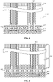
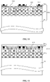
- FIG. 1 is a schematic diagram illustrating a sectional structure of a semiconductor structure according to an embodiment of the disclosure
- FIG. 2 is a schematic diagram illustrating another sectional structure of a semiconductor structure according to an embodiment of the disclosure
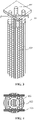
- FIG. 3 is a schematic diagram illustrating a local three-dimensional structure of a semiconductor structure according to an embodiment of the disclosure.
- the semiconductor structure in the embodiments of the disclosure includes a base 101, a conductive pillar 102 at least located in the base 101, connecting structures 103 and an electrical connection layer 104.
- At least one connecting structure 103 is electrically connected to an end of the conductive pillar 102, the material of the connecting structure 103 is different from that of the conductive pillar 102, and a total area of an orthographic projection of the connecting structure 103 on the base 101 is less than an area of an orthographic projection of the conductive pillar 102 on the base 101.
- the electrical connection layer 104 is electrically connected to an end of the connecting structure 103 distal from the conductive pillar 102.
- the conductive pillar 102 may implement an electric connection to the electrical connection layer 104 through one or more connecting structures 103, so as to implement the electric signal transmission between the conductive pillar 102 and the electrical connection layer 104.
- the total area of the orthographic projection of the connecting structure 103 on the base 101 is less than the area of the orthographic projection of the conductive pillar 102 on the base 101, such that both the connecting structure 103 and an area for designing the circuit layout are provided between the conductive pillar 102 and the electrical connection layer 104, which is beneficial to increase the area for designing the circuit layout in the semiconductor structure.
- the base 101 includes a substrate 111 and a dielectric layer 121 stacked in sequence, and the electrical connection layer 104 is located in the dielectric layer 121.
- the base 101 may also include a third dielectric layer 131, which is located at one side of the substrate 111 distal from the dielectric layer 121.
- each connecting structure 103 is located in the dielectric layer 121 and the substrate 111.
- the conductive pillar 102 is located in the third dielectric layer 131 and part of the substrate 111, so a spacing between the conductive pillar 102 and a first structure 105 is provided with the substrate 111 and the dielectric layer 121.
- the substrate 111 and the dielectric layer 121 may be used as stress buffer layers, to reduce the extrusion influence of the conductive pillar 102 on the first structure 105.
- each connecting structure 103 is only located in the dielectric layer 121, the conductive pillar 102 penetrates through the substrate 111 and is also located in part of the substrate 121, so a spacing between the conductive pillar 102 and the first structure 105 is provided with the dielectric layer 121.
- the dielectric layer 121 may be used as a stress buffer layer, to reduce the extrusion influence of the conductive pillar 102 on the first structure 105.
- the dielectric layer 121 and the third dielectric layer are material layers with low thermal expansion coefficient, for example, silicon dioxide layers, silicon oxide layers, silicon nitride layers, silicon carbon nitrogen.
- the substrate 111 is a semiconductor substrate, for example, a silicon substrate, a germanium substrate, a silicon germanium substrate or a silicon carbide substrate.
- the connecting structure 103 is provided with a first end surface and a second end surface opposite to the first end surface.
- the first end surface is embedded into the conductive pillar 102, and the second end surface is in contact with an end surface of the electrical connection layer 104.
- a position relationship among the connecting structure, the conductive pillar and the electrical connection layer may also be that: the first end surface is in contact with the end surface of the conductive pillar, and the second end surface is in contact with the end surface of the electrical connection layer, or the first end surface is embedded into the conductive pillar, and the second end surface is embedded into the electrical connection layer, or the first end surface is in contact with the end surface of the conductive pillar, and the second end surface is embedded into the electrical connection layer.
- the ratio of the total area of the orthographic projection of the connecting structure 103 on the substrate 101 to the area of the orthographic projection of the conductive pillar 102 on the substrate 101 is ranged from 1/10 to 1/5.
- a cross sectional area of the connecting structure 103 i.e., the area of the orthographic projection of the connecting structure 103 on the base 101
- a cross sectional area of the connecting structure 103 is smaller, such that there is an area for designing the circuit layer in the spacing between the conductive pillar 102 and the electrical connection layer 104, namely, another structure may be arranged, which is beneficial to improve the space utilization rate of the semiconductor structure.
- the conductive pillar 102 may be a TSV, which is usually made of copper, gold, silver, tungsten and other metal materials.
- thermal expansion coefficient of the material of the conductive pillar 102 is greater than that of the material of the connecting structure 103.
- the thermal expansion coefficient of the material of the connecting structure 103 may also be less than that of the material of the electrical connection layer 104.
- the circuit layout may also be designed in the area especially close to the connecting structure 103, further increasing the area for designing the circuit layout.
- thermal stress generated by the connecting structure 103 due to heating is small, and thus the extrusion influence of the connecting structure 103 on the conductive pillar 102 and the electrical connection layer 104 that are electrically connected to the connecting structure 103 is small, which is beneficial to improve the stability of the electrical connection of the connecting structure 103 with the conductive pillar 102 and the electrical connection layer 104.
- the material of the connecting structure 103 includes doped polycrystalline silicon and a metal material.
- the doped polycrystalline silicon includes P-type doped polycrystalline silicon and N-type doped polycrystalline silicon.
- the metal material includes at least one of metal materials with a low thermal expansion coefficient, for example, tungsten, titanium, gold, nickel and palladium.
- the semiconductor structure further includes at least one first structure 105, and part of the first structures 105 are arranged around a connecting structure 103 or interspersed in the intervals of the plurality of connecting structures 103.
- the first structures 105 are configured to generate or transmit the electric signal of the semiconductor structure.
- a part of the first structures 105 are arranged in the spacings between the conductive pillars 102 and the electrical connection layers 104, which is beneficial to increase the area for designing the circuit layout. Further, other structures arranged at the two sides of the conductive pillar 102 may implement the electric connection through the spacing between the conductive pillar 102 and the electrical connection layer 104, which is beneficial to improve the diversity of the electric connections between the structures in the semiconductor structure.
- the first structure may be an electronic component (a capacitor, a resistor, a potentiometer, etc.) or a wire.
- the embodiments of the disclosure do not make any limitation to the type of the first structure.
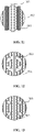
- FIG. 4 to FIG. 11 are schematic diagrams illustrating several plan structures of a structure composed of a conductive pillar, a connecting structure and a first structure in the semiconductor structure according to the embodiments of the disclosure
- FIG. 12 to FIG. 13 are schematic diagrams illustrating two plans structures of a structure composed of a conductive pillar and a connecting structure in a semiconductor structure according to the embodiments of the disclosure.
- one connecting structure 103 encloses a closed ring structure, and the first structures 105 are located around the connecting structure 103.
- a central axis of the connecting structure 103 coincides with that of the conductive pillar 102.
- the single connecting structure 103 is a closed circular ring structure, and the first structures 105 are in an elongated shape and located at the two sides of the connecting structure 103.
- the single connecting structure 103 is a closed square ring structure, and the first structures 105 are in an elongated shape and located at the two sides of the connecting structure 103.
- Example 2 referring to FIG.6 to FIG. 8 , at least two connecting structures 103 enclose a ring structure, and the first structure 105 is located in the spacing of the plurality of connecting structures 103.
- a central axis of the ring structure enclosed by the connecting structure 103 coincides with that of the conductive pillar 102.
- two connecting structures 103 enclose a circular ring structure
- the first structure 105 is in an elongated shape and located in the spacing of the two connecting structures 103.
- four connecting structures 103 enclose a circular ring structure
- the first structure 105 is cross-shaped, located at the central axis of the conductive pillar 102 and also located in the spacing of every two adjacent connecting structures 103.
- FIG. 7 referring to FIG.
- the first structure 105 is a combined structure formed by a square structure located at the central axis of the conductive pillar 102 and elongated structures at the two sides of the square structure.
- the structure located at the central axis of the conductive pillar may also be a rectangular structure, a circular structure, an elliptical structure or the like.
- Example 3 referring to FIG.9 and FIG. 10 , at least two connecting structures 103 are spaced around the central axis of the conductive pillar 102, and the first structures 105 are located in the spacing of the plurality of connecting structures 103.
- two connecting structures 103 are uniformly spaced around the central axis of the conductive pillar 102, the sectional shape of a connecting structure 103 (i.e., the shape of the orthographic projection of the connecting structure 103 on the base 101) is circular, the plurality of first structures 105 are uniformly arranged in the spacing of the two connecting structures 103, and the sectional shape of the first structure 105 (i.e., the shape of the orthographic projection of the first structure 105 on the base 101) is rectangular.
- the sectional shape of a connecting structure 103 i.e., the shape of the orthographic projection of the connecting structure 103 on the base 101
- the sectional shape of the first structure 105 i.e., the shape of the orthographic projection of the first structure 105 on the base 101
- connecting structures 103 are uniformly spaced around the central axis of the conductive pillar 102, the sectional shape of a connecting structure 103 is elliptical, the first structure 105 is cross-shaped, located at the central axis of the conductive pillar 102 and also located in the spacing of every two adjacent connecting structures 103.
- the connecting structure 103 and the first structures 105 are fin-shaped structures, and the first structures 105 are located at the two sides of the connecting structure 103.
- the central axis of the connecting structure 103 coincides with that of the conductive pillar 102, and the first structures 105 are mutually parallel to the connecting structure 103.
- the sectional shape of the conductive pillar 102 (i.e., the shape of the orthographic projection of the conductive pillar 102 on the base 101) is circular. In other embodiments, the sectional shape of the conductive pillar may also be other shapes.
- the embodiments of the disclosure do not actually limit the sectional shapes of the conductive pillar 102, the connecting structure 103 and the first structure 105.
- the first structure may also be not located in the spacing of the plurality of connecting structures 503, and the orthographic projection of the first structure on the base may also be not within the orthographic projection of the conductive pillar 502 in the base. Since there is a spacing between the conductive pillar 502 and the electrical connection layer, and there is no KOZ around the spacing area, the first structure may be located around the spacing area rather than being located in the spacing area, thereby increasing the area for designing the circuit layout in the semiconductor structure.
- the first structure is located at the two sides of the connecting structure or the first structure is located in the spacing of at least two connecting structures, and the orthographic projection of the first structure on the base is partially within the orthographic projection of the conductive pillar on the base, which is beneficial to design the circuit layout by using the spacing between the conductive pillar and the electrical connection layer, increase the design area of the circuit layout and improve the space utilization rate in the semiconductor structure.
- the embodiments of the disclosure further provide a semiconductor structure.
- the embodiments are substantially the same as the previous embodiments, and the main difference is that the connecting structure in the semiconductor structure is also electrically connected to the first structure.
- the semiconductor structure provided by the embodiments of the disclosure is described below in combination with the drawings. It is to be noted that the same or corresponding part as the previous the embodiments may make reference to the detail description of the previous the embodiments, which are not elaborated herein.
- FIG. 14 is a schematic diagram illustrating a sectional structure of a semiconductor structure according to an embodiment of the disclosure.
- the semiconductor structure includes a base 201, a conductive pillar 202 at least located in the base 201, at least two connecting structures 203 and a plurality of first structures 205, and an electrical connection layer 204.
- At least one connecting structure 203 is electrically connected to an end of the conductive pillar 203
- at least one connecting structure 203 is electrically to the first structure 205
- the materials of the connecting structures 203 are different from the material of the conductive pillar 202
- a total area of an orthographic projection of a connecting structure 203 on the base 201 is less than an area of an orthographic projection of the conductive pillar 202 on the base 201.
- the electrical connection layer 204 is electrically connected to an end of the connecting structures 203 distal from the conductive pillar 202.
- the electric signal transmitted by the conductive pillar 202 may be only transmitted to the electrical connection layer 204 through the connecting structures 203, and may also be transmitted to the electrical connection layer 204 through a connecting structure 203 and then transmitted to the first structure 205 through a connecting structure 203, which is beneficial to improve the diversity of the signal transmission in the semiconductor structure.
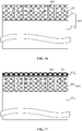
- FIG. 15 to FIG. 20 are schematic diagrams illustrating sectional structures corresponding to various steps of the method for manufacturing a semiconductor structure according to an embodiment of the disclosure.
- FIG. 21 to FIG. 25 are schematic diagrams illustrating sectional structures corresponding to various steps of another method for manufacturing a semiconductor structure according to an embodiment of the disclosure.
- the method for manufacturing the semiconductor includes the following operations. Referring to FIG. 15 to FIG. 20 , a base 301 is provided, and the base 301 has a first surface and a second surface opposite to the first surface.
- the base 301 includes a substrate 311 and a first dielectric layer 341 stacked in sequence.
- the first surface is a surface of the first dielectric layer 341, and a plurality of first structures 305 are arranged in the first dielectric layer 341.
- a connecting structure 303, an electrical connection layer 304 and a conductive pillar 302 may be subsequently formed on the base 301.
- the connecting structure 303 and the electrical connection layer 304 are formed firstly, and then the conductive pillar 302 is formed. Details are made below.
- the base 301 is etched to form a plurality of first vias 313 and a plurality of second vias 312.
- the first surface exposes the first vias 313, and the second surface exposes the second vias 312.
- the second vias 312 are formed after firstly forming the first vias 313.
- the operation of forming the first vias 313 and the second vias 312 includes the following steps.
- the first dielectric layer 341 is etched to form the plurality of first vias 313, and the first vias 313 are located in the spacings of the first structures 305.
- the etching process of forming the first vias 313 is as follows.
- a first photoresist pattern is formed on the first dielectric layer 341 by using a first photomask, and the first dielectric layer 341 is etched by using the first photoresist pattern as a mask to form the first vias 313.
- the first vias 313 (referring to FIG. 15 ) are filled to form the connecting structures 303.
- the filling material may include a silicon-containing material and a metal material.
- the silicon-containing material may include at least one of silicon, silicon oxide, silicon nitride, silicon oxynitride, silicon carbide, silicon carbon nitrogen or silicon carbon oxide.
- the metal material may include a metal material with a low thermal expansion coefficient, such as at least one of tungsten, titanium, gold, nickel, or palladium. It is to be noted that the filling material for filling the plurality of first vias 313 in the same semiconductor may be the same or different.
- the process for forming the electrical connection layer at one side of the connecting structure includes the following operations.
- a second dielectric layer 351 is formed on the first dielectric layer 341.
- the polishing method includes chemical mechanical polishing.
- the second dielectric layer 351 is etched to form one or more third vias 314, and each third via 314 exposes one or more connecting structures 303.
- the etching process for forming the third vias 314 is as follows.
- a third photoresist pattern is formed on the second dielectric layer 351 by using a third photomask, and the second dielectric layer 351 is etched by using the third photoresist pattern as a mask to form the third vias 314.
- a third via 314 may only expose a surface of an end of the connecting structure 303, namely, the surface of the end of the connecting structure 303 is in contact with a surface of an end of the electrical connection layer subsequently formed.
- the third via may also expose a part of one side of the connecting structure, namely, part of the connecting structure may be embedded into the electrical connection layer subsequently formed.
- each third via 314 is filled to form the electrical connection layer 304.
- a fifth dielectric layer 361 is also formed at one side of the second dielectric layer 351 that exposes the surface of the electrical connection layer 304, to avoid exposure of the electrical connection layer 304 outside the semiconductor structure and prevent the electrical connection layer 304 from falling off the semiconductor structure.
- the first dielectric layer 341, the second dielectric layer 351 and the fifth dielectric layer 361 form the dielectric layer 321 together (the dielectric layer 312 corresponds to the dielectric layer 121 in FIG. 2 of the above embodiment).
- the first dielectric layer 341, the second dielectric layer 351 and the fifth dielectric layer 361 all are the material layers with low thermal expansion coefficients, such as silicon dioxide layers, silicon oxide layers or silicon nitride layers, silicon carbon nitrogen.
- the process for forming the second vias 312 and filling the second vias 312 to form the conductive pillars 302 includes the following operations.
- a third dielectric layer 331 is formed at one side, distal from the first dielectric layer 341, of the substrate 311.
- the third dielectric layer 331, the substrate 311 and the first dielectric layer 341 are etched to form the second vias 312, and the second vias 312 expose the connecting structures 303.
- the polishing method includes chemical mechanical polishing.
- the etching process for forming the second vias 312 is as follows.
- a second photoresist pattern is formed on the third dielectric layer 331 by using a second photomask, and the third dielectric layer 331 is etched by using the second photoresist pattern as a mask to form the second vias 312.
- a second via 312 may expose a part of one side of the connecting structure 303, namely, part of the connecting structure 303 may be embedded into the conductive pillar subsequently formed.
- the second via may also expose a surface of an end of the connecting structure, namely, the surface of the end of the connecting structure is in contact with a surface of an end of the conductive pillar subsequently formed.
- each second via 312 (referring to FIG. 20 ) is filled to form the conductive pillar 102.
- the filling material for forming the conductive pillar 102 is copper. In other embodiments, the filling material for forming the conductive pillar 102 may be other metal materials, such as gold, silver or tungsten.
- the connecting structure 303 is electrically connected to the end of the conductive pillar 302, the material for forming the connecting structure 303 is different from that for forming the conductive pillar 302, and the total area of the orthographic projection of the connecting structure 303 on the base 301 is less than the area of the orthographic projection of the conductive pillar 302 on the base 301.
- the conductive pillar 302 is formed on the base 301 firstly, and then the connecting structure 303 and the electrical connection layer 304 are formed.
- the surface of the substrate 311 distal from the first dielectric layer 341 is polished, and for example, the polishing method includes chemical mechanical polishing. Then, the third dielectric layer 331 is formed at one side of the substrate 311 distal from the first dielectric layer 341.
- the third dielectric layer 331 and the substrate 311 are etched to form one or more second vias 312.
- each second via 312 is filled to form the conductive structure 302.
- the first dielectric layer 341 is etched to form the plurality of first vias, and the first vias are located in the spacings of the first structures 30. Each first via is filled to form the connecting structure 303.
- the second dielectric layer 351 is formed on the first dielectric layer 341.
- the polishing method includes chemical mechanical polishing.
- the second dielectric layer 351 is etched to form one or more third via 314, and each third via 314 exposes the connecting structure 303.
- the third via 314 (referring to FIG. 25 ) is filled to form the electrical connection layer 104.
- the etching process for forming the first vias 313, the second vias 312 and the third vias 314 may be the same as the above embodiments.
- a process step for manufacturing the connecting structure is added in the process for manufacturing the conductive pillar and the electrical connection layer, and the total area of the orthographic projection of the connecting structure on the base is less than the area of the orthographic projection of the conductive pillar on the base, so that the stability of the electric signal transmission between the conductive pillar and the electrical connection layer may be ensured through a small connecting structure.
- the first structures may be arranged around the connecting structure and in the spacings of the plurality of connecting structures, which is beneficial to increase the area for designing the circuit layout in the semiconductor structure.
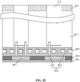
- FIG. 26 to FIG. 32 are schematic diagrams illustrating sectional structures corresponding to various steps of a method for manufacturing a semiconductor structure according to an embodiment of the disclosure. The same or corresponding part as the previous embodiments may make reference to the corresponding description of the previous embodiments, which are not elaborated below.
- the base 401 includes a substrate 411 and a first dielectric layer 441 stacked in sequence, the first surface is a surface of the first dielectric layer 441, and a plurality of first structures 405 are arranged in the first dielectric layer 441.
- the connecting structure 403 and the electrical connection layer 404 are firstly formed, and then the conductive pillar 402 is formed. Details are made below.
- the first dielectric layer 441 is etched to form the plurality of first vias 413, and at least one first via 413 exposes the first structure 405.
- the connecting structure 403 includes a first connecting structure 423 and a second connecting structure 433.
- the first connecting structure 423 is in contact with the first structure 405, and the second connecting structure 433 is located in the spacing between the adjacent first structures 405.
- the second dielectric layer 451 is formed on the first dielectric layer 441.
- the second dielectric layer 451 is etched to form a third via 414, and the third via 414 exposes the first connecting structure 423 and the second connecting structure 433.
- the third via 414 (referring to FIG. 28 ) is filled to form the electrical connection layer 404.
- a fifth dielectric layer 461 is also formed at one side of the second dielectric layer 451 that exposes the surface of the electrical connection layer 404. It is to be noted that, in the embodiments of the disclosure, the first dielectric layer 441, the second dielectric layer 451 and the fifth dielectric layer 461 form the dielectric layer 421 together (the dielectric layer 421 corresponds to the dielectric layer 221 in FIG. 14 of the above the embodiment).
- the surface of the substrate 411 distal from the first dielectric layer 441 is polished, for example, the polishing method includes chemical mechanical polishing. Then, the third dielectric layer 431 is formed at one side, distal from the first dielectric layer 441, of the substrate 411.
- the third dielectric layer 431 and the substrate 411 are etched to form a second via 412, and the second via 412 exposes the second connecting structure 433.
- the second via 412 (referring to FIG. 32 ) is filled to form the conductive pillar 202.
- the connecting structure when the connecting structure is manufactured, at least one connecting structure is electrically connected to the conductive pillar, and at least one connecting structure is electrically connected to the first structure, such that the electric signal transmitted by the conductive pillar may be transmitted to the first structures through the electrical connection layer, which is beneficial to improve the diversity of the signal transmission in the semiconductor structure.
Landscapes
- Internal Circuitry In Semiconductor Integrated Circuit Devices (AREA)
Abstract
Description
- This application is based upon and claims priority to
Chinese Patent Application No. 202011281266.X, filed on November 16, 2020 - The embodiments of the disclosure relate, but are not limited to a semiconductor structure and a method for manufacturing the same.
- Interconnection between chips or wafers in a semiconductor structure may be implemented through manufacturing via holes in a perpendicular direction, and the interconnection technology is called as a Through Silicon Via (TSV) technology. The traditional TSV is usually filled with a metal material to form a conductive pillar, and an end surface of the conductive pillar is in contact and electric connection with another electrical connection layer to implement electric connection among different layers.
- However, when the end surface of the conductive pillar directly contacts with that of the electrical connection layer, no spacing is provided between the conductive pillar and the electrical connection layer, so a circuit may not be designed between the conductive pillar and the electrical connection layer. In addition, when the conductive pillar expands due to heating, it is easy to cause extrusion on a structure adjacent to the conductive pillar, so a semiconductor Keep Out Zone (KOZ) is also arranged around the conductive pillar, and circuit layout and design cannot be performed in the KOZ. Therefore, the direct contact of the conductive pillar and the electrical connection layer and the existence of the KOZ may reduce an area for designing the circuit layout.
- The embodiments of the disclosure provide a semiconductor structure. The semiconductor structure includes a base, a conductive pillar at least located in the base, connecting structures and an electrical connection layer. At least one connecting structure is electrically connected to an end of the conductive pillar, the material of the connecting structure is different from that of the conductive pillar, and a total area of an orthographic projection of the connecting structure on the base is less than an area of an orthographic projection of the conductive pillar on the base. The electrical connection layer is electrically connected to an end of the connecting structure distal from the conductive pillar.
- The embodiments of the disclosure further provide a method for manufacturing a semiconductor structure. The method includes the following operations. A base is provided, and the base has a first surface and an opposite second surface. The base is etched to form a plurality of first vias and a plurality of second vias, the first surface exposes the first vias, and the second surface exposes the second vias. The first vias are filled to form connecting structures, the second vias are filled to form conductive pillars, at least one connecting structure is electrically connected to an end of one of the conductive pillars, the material forming the connecting structure is different from that forming the conductive pillar, and a total area of an orthographic projection of the connecting structure on the base is less than an area of an orthographic projection of the conductive pillar on the base. An electrical connection layer is formed at one side of the connecting structure distal from the conductive pillar.
- One or more the embodiments are illustrated by pictures in the corresponding drawings. The pictures in the drawings do not constitute a proportional restriction unless stated otherwise.
-
FIG. 1 is a schematic diagram illustrating a sectional structure of a semiconductor structure according to an embodiment of the disclosure. -
FIG. 2 is a schematic diagram illustrating another sectional structure of a semiconductor structure according to an embodiment of the disclosure. -
FIG. 3 is a schematic diagram illustrating a local three-dimensional structure of a semiconductor structure according to an embodiment of the disclosure. -
FIG. 4 to FIG. 11 are schematic diagrams illustrating several plan views of a structure composed of a conductive pillar, a connecting structure and a first structure in a semiconductor structure according to embodiments of the disclosure. -
FIG. 12 to FIG. 13 are schematic diagrams illustrating two plan views of a structure composed of a conductive pillar and a connecting structure in a semiconductor structure according to embodiments of the disclosure. -
FIG. 14 is a schematic diagram illustrating a sectional structure of a semiconductor structure according to an embodiment of the disclosure. -
FIG. 15 to FIG. 20 are schematic diagrams illustrating sectional structures corresponding to various steps of a method for manufacturing a semiconductor structure according to embodiments of the disclosure. -
FIG. 21 to FIG. 25 are schematic diagrams illustrating sectional structures corresponding to various steps of another method for manufacturing a semiconductor structure according to embodiments of the disclosure. -
FIG. 26 to FIG. 32 are schematic diagrams illustrating sectional structures corresponding to various steps of a method for manufacturing a semiconductor structure according to embodiments of the disclosure. - It is to known from the background that, in the related art, the direct contact of the conductive pillar and the electrical connection layer and the existence of the KOZ may reduce an area for designing the circuit layout.
- It has been found through analysis that a blank area where the conductive pillar is designed needs to be reserved when designing the circuit layout in the semiconductor structure, such that the conductive pillar may subsequently pass through the reserved blank area, but in such case, the area for designing the circuit layout may be reduced. In addition, an area close to the conductive pillar is easily affected by thermal stress when the conductive pillar is thermally expanded, so a peripheral area (KOZ) close the conductive pillar is unavailable for the circuit layout and design, further reducing the area for designing the circuit layout.
- The embodiments of the disclosure provide a semiconductor structure, in which a conductive pillar is connected to an electrical connection layer through a connecting structure, and a total area of an orthographic projection of the connecting structure on a base is less than an area of an orthographic projection of the conductive pillar on the base. A current of an electric signal transferred by the conductive pillar is relatively small, and thus it is not necessary for the whole end surface of the conductive pillar to be in contact with the electrical connection layer, and the stability of the electric signal transmission between the conductive pillar and the electrical connection layer may be ensured through a small connecting structure. Further, the material of the connecting structure is different from that of the conductive pillar, and a periphery of the connecting structure and intervals of a plurality of connecting structures may be used for design of the circuit layout, which is beneficial to increase the area for designing the circuit layout in the semiconductor structure.
- Various embodiments of the disclosure are described in details below in combination with the drawings. However, those of ordinary skill in the art may understand that, in various embodiments of the disclosure, technical details are provided for readers to understand the disclosure better., but even without these technical details as well as various changes and modifications based on the embodiments below, the technical solution protected by the disclosure may also be implemented.
-
FIG. 1 is a schematic diagram illustrating a sectional structure of a semiconductor structure according to an embodiment of the disclosure,FIG. 2 is a schematic diagram illustrating another sectional structure of a semiconductor structure according to an embodiment of the disclosure, andFIG. 3 is a schematic diagram illustrating a local three-dimensional structure of a semiconductor structure according to an embodiment of the disclosure. - Referring to
FIG. 1 , the semiconductor structure in the embodiments of the disclosure includes abase 101, aconductive pillar 102 at least located in thebase 101, connectingstructures 103 and anelectrical connection layer 104. At least one connectingstructure 103 is electrically connected to an end of theconductive pillar 102, the material of the connectingstructure 103 is different from that of theconductive pillar 102, and a total area of an orthographic projection of the connectingstructure 103 on thebase 101 is less than an area of an orthographic projection of theconductive pillar 102 on thebase 101. Theelectrical connection layer 104 is electrically connected to an end of the connectingstructure 103 distal from theconductive pillar 102. - In the embodiments of the disclosure, the
conductive pillar 102 may implement an electric connection to theelectrical connection layer 104 through one or moreconnecting structures 103, so as to implement the electric signal transmission between theconductive pillar 102 and theelectrical connection layer 104. In addition, the total area of the orthographic projection of theconnecting structure 103 on thebase 101 is less than the area of the orthographic projection of theconductive pillar 102 on thebase 101, such that both theconnecting structure 103 and an area for designing the circuit layout are provided between theconductive pillar 102 and theelectrical connection layer 104, which is beneficial to increase the area for designing the circuit layout in the semiconductor structure. - In some embodiments, the
base 101 includes a substrate 111 and adielectric layer 121 stacked in sequence, and theelectrical connection layer 104 is located in thedielectric layer 121. In other embodiments, thebase 101 may also include a thirddielectric layer 131, which is located at one side of the substrate 111 distal from thedielectric layer 121. - In an example, still referring to
FIG. 1 , each connectingstructure 103 is located in thedielectric layer 121 and the substrate 111. Correspondingly, theconductive pillar 102 is located in the thirddielectric layer 131 and part of the substrate 111, so a spacing between theconductive pillar 102 and afirst structure 105 is provided with the substrate 111 and thedielectric layer 121. When theconductive pillars 102 is thermally expanded, the substrate 111 and thedielectric layer 121 may be used as stress buffer layers, to reduce the extrusion influence of theconductive pillar 102 on thefirst structure 105. - In some embodiments, referring to
FIG. 2 , each connectingstructure 103 is only located in thedielectric layer 121, theconductive pillar 102 penetrates through the substrate 111 and is also located in part of thesubstrate 121, so a spacing between theconductive pillar 102 and thefirst structure 105 is provided with thedielectric layer 121. When theconductive pillar 102 is thermally expanded, thedielectric layer 121 may be used as a stress buffer layer, to reduce the extrusion influence of theconductive pillar 102 on thefirst structure 105. - In the embodiments of the disclosure, the
dielectric layer 121 and the third dielectric layer are material layers with low thermal expansion coefficient, for example, silicon dioxide layers, silicon oxide layers, silicon nitride layers, silicon carbon nitrogen. The substrate 111 is a semiconductor substrate, for example, a silicon substrate, a germanium substrate, a silicon germanium substrate or a silicon carbide substrate. - Referring to
FIG. 3 , the connectingstructure 103 is provided with a first end surface and a second end surface opposite to the first end surface. The first end surface is embedded into theconductive pillar 102, and the second end surface is in contact with an end surface of theelectrical connection layer 104. In other embodiments, a position relationship among the connecting structure, the conductive pillar and the electrical connection layer may also be that: the first end surface is in contact with the end surface of the conductive pillar, and the second end surface is in contact with the end surface of the electrical connection layer, or the first end surface is embedded into the conductive pillar, and the second end surface is embedded into the electrical connection layer, or the first end surface is in contact with the end surface of the conductive pillar, and the second end surface is embedded into the electrical connection layer. - The ratio of the total area of the orthographic projection of the
connecting structure 103 on thesubstrate 101 to the area of the orthographic projection of theconductive pillar 102 on thesubstrate 101 is ranged from 1/10 to 1/5. - In the embodiments of the disclosure, compared with a cross sectional area of the conductive pillar 102 (i.e., the area of the orthographic projection of the
conductive pillar 102 on the base 101), a cross sectional area of the connecting structure 103 (i.e., the area of the orthographic projection of theconnecting structure 103 on the base 101) is smaller, such that there is an area for designing the circuit layer in the spacing between theconductive pillar 102 and theelectrical connection layer 104, namely, another structure may be arranged, which is beneficial to improve the space utilization rate of the semiconductor structure. Moreover, under a premise of ensuring the stability of the electric signal transmission between theconductive pillar 102 and theelectrical connection layer 104, the smaller the ratio of the cross sectional area of the connectingstructure 103 to the cross sectional area of theconductive pillar 102, the greater the area for designing the circuit layout. - In the embodiments of the disclosure, the
conductive pillar 102 may be a TSV, which is usually made of copper, gold, silver, tungsten and other metal materials. - In addition, the thermal expansion coefficient of the material of the
conductive pillar 102 is greater than that of the material of the connectingstructure 103. The thermal expansion coefficient of the material of the connectingstructure 103 may also be less than that of the material of theelectrical connection layer 104. - Therefore, when a temperature of an environment where the semiconductor structure is located is high, a significant volume expansion is not occurred to the connecting
structure 103 when the connectingstructure 103 is heated, the generated thermal stress is small, so there is no significant extrusion influence on a structure around the connectingstructure 103, and the circuit layout may also be designed in the area especially close to the connectingstructure 103, further increasing the area for designing the circuit layout. In addition, thermal stress generated by the connectingstructure 103 due to heating is small, and thus the extrusion influence of the connectingstructure 103 on theconductive pillar 102 and theelectrical connection layer 104 that are electrically connected to the connectingstructure 103 is small, which is beneficial to improve the stability of the electrical connection of the connectingstructure 103 with theconductive pillar 102 and theelectrical connection layer 104. - The material of the connecting
structure 103 includes doped polycrystalline silicon and a metal material. - In some embodiments, the doped polycrystalline silicon includes P-type doped polycrystalline silicon and N-type doped polycrystalline silicon. The metal material includes at least one of metal materials with a low thermal expansion coefficient, for example, tungsten, titanium, gold, nickel and palladium.
- In the embodiments of the disclosure, still referring to
FIG. 1 , the semiconductor structure further includes at least onefirst structure 105, and part of thefirst structures 105 are arranged around a connectingstructure 103 or interspersed in the intervals of the plurality of connectingstructures 103. Thefirst structures 105 are configured to generate or transmit the electric signal of the semiconductor structure. - A part of the
first structures 105 are arranged in the spacings between theconductive pillars 102 and the electrical connection layers 104, which is beneficial to increase the area for designing the circuit layout. Further, other structures arranged at the two sides of theconductive pillar 102 may implement the electric connection through the spacing between theconductive pillar 102 and theelectrical connection layer 104, which is beneficial to improve the diversity of the electric connections between the structures in the semiconductor structure. - It is to be noted that the first structure may be an electronic component (a capacitor, a resistor, a potentiometer, etc.) or a wire. The embodiments of the disclosure do not make any limitation to the type of the first structure.
- In the embodiments of the disclosure, the distribution of part of the
connection structures 103 and thefirst structures 105 in the semiconductor structure may be described below in combination withFIG. 4 to FIG. 11. FIG. 4 to FIG. 11 are schematic diagrams illustrating several plan structures of a structure composed of a conductive pillar, a connecting structure and a first structure in the semiconductor structure according to the embodiments of the disclosure, andFIG. 12 to FIG. 13 are schematic diagrams illustrating two plans structures of a structure composed of a conductive pillar and a connecting structure in a semiconductor structure according to the embodiments of the disclosure. - In Example 1, referring to
FIG.4 andFIG. 5 , one connectingstructure 103 encloses a closed ring structure, and thefirst structures 105 are located around the connectingstructure 103. A central axis of the connectingstructure 103 coincides with that of theconductive pillar 102. - In some embodiments, referring to
FIG. 4 , the single connectingstructure 103 is a closed circular ring structure, and thefirst structures 105 are in an elongated shape and located at the two sides of the connectingstructure 103. Alternatively, referring toFIG. 5 , the single connectingstructure 103 is a closed square ring structure, and thefirst structures 105 are in an elongated shape and located at the two sides of the connectingstructure 103. - In Example 2, referring to
FIG.6 to FIG. 8 , at least two connectingstructures 103 enclose a ring structure, and thefirst structure 105 is located in the spacing of the plurality of connectingstructures 103. A central axis of the ring structure enclosed by the connectingstructure 103 coincides with that of theconductive pillar 102. - In some embodiments, referring to
FIG. 6 , two connectingstructures 103 enclose a circular ring structure, and thefirst structure 105 is in an elongated shape and located in the spacing of the two connectingstructures 103. Alternatively, referring toFIG. 7 , four connectingstructures 103 enclose a circular ring structure, thefirst structure 105 is cross-shaped, located at the central axis of theconductive pillar 102 and also located in the spacing of every two adjacent connectingstructures 103. Alternatively, referring toFIG. 8 , two connectingstructures 103 enclose a square ring structure, thefirst structure 105 is a combined structure formed by a square structure located at the central axis of theconductive pillar 102 and elongated structures at the two sides of the square structure. In other embodiments, the structure located at the central axis of the conductive pillar may also be a rectangular structure, a circular structure, an elliptical structure or the like. - In Example 3, referring to
FIG.9 and FIG. 10 , at least two connectingstructures 103 are spaced around the central axis of theconductive pillar 102, and thefirst structures 105 are located in the spacing of the plurality of connectingstructures 103. - In some embodiments, referring to
FIG. 9 , two connectingstructures 103 are uniformly spaced around the central axis of theconductive pillar 102, the sectional shape of a connecting structure 103 (i.e., the shape of the orthographic projection of the connectingstructure 103 on the base 101) is circular, the plurality offirst structures 105 are uniformly arranged in the spacing of the two connectingstructures 103, and the sectional shape of the first structure 105 (i.e., the shape of the orthographic projection of thefirst structure 105 on the base 101) is rectangular. Alternatively, referring toFIG. 10 , four connectingstructures 103 are uniformly spaced around the central axis of theconductive pillar 102, the sectional shape of a connectingstructure 103 is elliptical, thefirst structure 105 is cross-shaped, located at the central axis of theconductive pillar 102 and also located in the spacing of every two adjacent connectingstructures 103. - In Example 4, referring to
FIG. 11 , the connectingstructure 103 and thefirst structures 105 are fin-shaped structures, and thefirst structures 105 are located at the two sides of the connectingstructure 103. The central axis of the connectingstructure 103 coincides with that of theconductive pillar 102, and thefirst structures 105 are mutually parallel to the connectingstructure 103. - It is to be noted that, in the Example 1 to Example 4, the sectional shape of the conductive pillar 102 (i.e., the shape of the orthographic projection of the
conductive pillar 102 on the base 101) is circular. In other embodiments, the sectional shape of the conductive pillar may also be other shapes. - In the case that the
conductive pillar 102, the connectingstructure 103 and thefirst structure 105 meet the position relationship of any one of the above situations, the embodiments of the disclosure do not actually limit the sectional shapes of theconductive pillar 102, the connectingstructure 103 and thefirst structure 105. - In other embodiments, referring to
FIG. 12 and FIG. 13 , the first structure may also be not located in the spacing of the plurality of connectingstructures 503, and the orthographic projection of the first structure on the base may also be not within the orthographic projection of theconductive pillar 502 in the base. Since there is a spacing between theconductive pillar 502 and the electrical connection layer, and there is no KOZ around the spacing area, the first structure may be located around the spacing area rather than being located in the spacing area, thereby increasing the area for designing the circuit layout in the semiconductor structure. - In the embodiments of the disclosure, the first structure is located at the two sides of the connecting structure or the first structure is located in the spacing of at least two connecting structures, and the orthographic projection of the first structure on the base is partially within the orthographic projection of the conductive pillar on the base, which is beneficial to design the circuit layout by using the spacing between the conductive pillar and the electrical connection layer, increase the design area of the circuit layout and improve the space utilization rate in the semiconductor structure.
- The embodiments of the disclosure further provide a semiconductor structure. The embodiments are substantially the same as the previous embodiments, and the main difference is that the connecting structure in the semiconductor structure is also electrically connected to the first structure. The semiconductor structure provided by the embodiments of the disclosure is described below in combination with the drawings. It is to be noted that the same or corresponding part as the previous the embodiments may make reference to the detail description of the previous the embodiments, which are not elaborated herein.
-
FIG. 14 is a schematic diagram illustrating a sectional structure of a semiconductor structure according to an embodiment of the disclosure. - Referring to
FIG. 14 , in the embodiment of the disclosure, the semiconductor structure includes abase 201, aconductive pillar 202 at least located in thebase 201, at least two connectingstructures 203 and a plurality offirst structures 205, and anelectrical connection layer 204. At least one connectingstructure 203 is electrically connected to an end of theconductive pillar 203, at least one connectingstructure 203 is electrically to thefirst structure 205, the materials of the connectingstructures 203 are different from the material of theconductive pillar 202, and a total area of an orthographic projection of a connectingstructure 203 on thebase 201 is less than an area of an orthographic projection of theconductive pillar 202 on thebase 201. Theelectrical connection layer 204 is electrically connected to an end of the connectingstructures 203 distal from theconductive pillar 202. - In the embodiments of the disclosure, the electric signal transmitted by the
conductive pillar 202 may be only transmitted to theelectrical connection layer 204 through the connectingstructures 203, and may also be transmitted to theelectrical connection layer 204 through a connectingstructure 203 and then transmitted to thefirst structure 205 through a connectingstructure 203, which is beneficial to improve the diversity of the signal transmission in the semiconductor structure. - The embodiments of the disclosure further provide a method for manufacturing a semiconductor structure, and the method may be used for manufacturing the semiconductor structure provided by the above the embodiments.
FIG. 15 to FIG. 20 are schematic diagrams illustrating sectional structures corresponding to various steps of the method for manufacturing a semiconductor structure according to an embodiment of the disclosure.FIG. 21 to FIG. 25 are schematic diagrams illustrating sectional structures corresponding to various steps of another method for manufacturing a semiconductor structure according to an embodiment of the disclosure. - In the embodiments of the disclosure, the method for manufacturing the semiconductor includes the following operations. Referring to
FIG. 15 to FIG. 20 , abase 301 is provided, and thebase 301 has a first surface and a second surface opposite to the first surface. - In some embodiments, the
base 301 includes asubstrate 311 and a firstdielectric layer 341 stacked in sequence. The first surface is a surface of thefirst dielectric layer 341, and a plurality offirst structures 305 are arranged in thefirst dielectric layer 341. - A connecting
structure 303, anelectrical connection layer 304 and aconductive pillar 302 may be subsequently formed on thebase 301. In the embodiments of the disclosure, the connectingstructure 303 and theelectrical connection layer 304 are formed firstly, and then theconductive pillar 302 is formed. Details are made below. - Referring to
FIG. 15 to FIG. 20 , thebase 301 is etched to form a plurality offirst vias 313 and a plurality ofsecond vias 312. The first surface exposes thefirst vias 313, and the second surface exposes thesecond vias 312. - In the embodiments of the disclosure, the
second vias 312 are formed after firstly forming thefirst vias 313. In some embodiments of the disclosure, the operation of forming thefirst vias 313 and thesecond vias 312 includes the following steps. - Referring to
FIG. 15 , thefirst dielectric layer 341 is etched to form the plurality offirst vias 313, and thefirst vias 313 are located in the spacings of thefirst structures 305. - In some embodiments, the etching process of forming the
first vias 313 is as follows. A first photoresist pattern is formed on thefirst dielectric layer 341 by using a first photomask, and thefirst dielectric layer 341 is etched by using the first photoresist pattern as a mask to form thefirst vias 313. - Referring to
FIG. 16 , the first vias 313 (referring toFIG. 15 ) are filled to form the connectingstructures 303. - In some embodiments, the filling material may include a silicon-containing material and a metal material. In some embodiments, the silicon-containing material may include at least one of silicon, silicon oxide, silicon nitride, silicon oxynitride, silicon carbide, silicon carbon nitrogen or silicon carbon oxide. The metal material may include a metal material with a low thermal expansion coefficient, such as at least one of tungsten, titanium, gold, nickel, or palladium. It is to be noted that the filling material for filling the plurality of
first vias 313 in the same semiconductor may be the same or different. - In the embodiments of the disclosure, the process for forming the electrical connection layer at one side of the connecting structure includes the following operations.
- Referring to
FIG. 17 , asecond dielectric layer 351 is formed on thefirst dielectric layer 341. - In some embodiments, after the connecting
structures 303 are formed and before thesecond dielectric layer 351 is formed, one side of thefirst dielectric layer 341 that exposes the surface of the connectingstructure 303 is polished. For example, the polishing method includes chemical mechanical polishing. - Referring to
FIG. 18 , thesecond dielectric layer 351 is etched to form one or morethird vias 314, and each third via 314 exposes one or more connectingstructures 303. - In some embodiments, the etching process for forming the
third vias 314 is as follows. A third photoresist pattern is formed on thesecond dielectric layer 351 by using a third photomask, and thesecond dielectric layer 351 is etched by using the third photoresist pattern as a mask to form thethird vias 314. - In the embodiments of the disclosure, a third via 314 may only expose a surface of an end of the connecting
structure 303, namely, the surface of the end of the connectingstructure 303 is in contact with a surface of an end of the electrical connection layer subsequently formed. In other embodiments, the third via may also expose a part of one side of the connecting structure, namely, part of the connecting structure may be embedded into the electrical connection layer subsequently formed. - Referring to
FIG. 19 , each third via 314 is filled to form theelectrical connection layer 304. - In the embodiments of the disclosure, after the
electrical connection layer 304 is formed, a fifthdielectric layer 361 is also formed at one side of thesecond dielectric layer 351 that exposes the surface of theelectrical connection layer 304, to avoid exposure of theelectrical connection layer 304 outside the semiconductor structure and prevent theelectrical connection layer 304 from falling off the semiconductor structure. - It is to be noted that, in the embodiments of the disclosure, the
first dielectric layer 341, thesecond dielectric layer 351 and thefifth dielectric layer 361 form thedielectric layer 321 together (thedielectric layer 312 corresponds to thedielectric layer 121 inFIG. 2 of the above embodiment). Thefirst dielectric layer 341, thesecond dielectric layer 351 and thefifth dielectric layer 361 all are the material layers with low thermal expansion coefficients, such as silicon dioxide layers, silicon oxide layers or silicon nitride layers, silicon carbon nitrogen. - In the embodiments of the disclosure, the process for forming the
second vias 312 and filling thesecond vias 312 to form theconductive pillars 302 includes the following operations. - Referring to
FIG. 20 , a thirddielectric layer 331 is formed at one side, distal from thefirst dielectric layer 341, of thesubstrate 311. The thirddielectric layer 331, thesubstrate 311 and thefirst dielectric layer 341 are etched to form thesecond vias 312, and thesecond vias 312 expose the connectingstructures 303. - In the embodiments of the disclosure, before the third
dielectric layer 331 is formed, the surface of thesubstrate 311 distal from thefirst dielectric layer 341 is polished, and for example, the polishing method includes chemical mechanical polishing. - In some embodiments, the etching process for forming the
second vias 312 is as follows. A second photoresist pattern is formed on the thirddielectric layer 331 by using a second photomask, and the thirddielectric layer 331 is etched by using the second photoresist pattern as a mask to form thesecond vias 312. - In the embodiments of the disclosure, a second via 312 may expose a part of one side of the connecting
structure 303, namely, part of the connectingstructure 303 may be embedded into the conductive pillar subsequently formed. In other embodiments, the second via may also expose a surface of an end of the connecting structure, namely, the surface of the end of the connecting structure is in contact with a surface of an end of the conductive pillar subsequently formed. - Still referring to
FIG. 2 , each second via 312 (referring toFIG. 20 ) is filled to form theconductive pillar 102. - In the embodiments of the disclosure, the filling material for forming the
conductive pillar 102 is copper. In other embodiments, the filling material for forming theconductive pillar 102 may be other metal materials, such as gold, silver or tungsten. - In the semiconductor structure provided by the embodiments of the disclosure, the connecting
structure 303 is electrically connected to the end of theconductive pillar 302, the material for forming the connectingstructure 303 is different from that for forming theconductive pillar 302, and the total area of the orthographic projection of the connectingstructure 303 on thebase 301 is less than the area of the orthographic projection of theconductive pillar 302 on thebase 301. - In other embodiments, referring to
FIG. 21 to FIG. 25 , theconductive pillar 302 is formed on the base 301 firstly, and then the connectingstructure 303 and theelectrical connection layer 304 are formed. - In some embodiments, referring to
FIG. 21 , the surface of thesubstrate 311 distal from thefirst dielectric layer 341 is polished, and for example, the polishing method includes chemical mechanical polishing. Then, the thirddielectric layer 331 is formed at one side of thesubstrate 311 distal from thefirst dielectric layer 341. - Referring to
FIG. 22 , the thirddielectric layer 331 and thesubstrate 311 are etched to form one or moresecond vias 312. - Referring to
FIG. 23 , each second via 312 is filled to form theconductive structure 302. - Referring to
FIG. 24 , thefirst dielectric layer 341 is etched to form the plurality of first vias, and the first vias are located in the spacings of the first structures 30. Each first via is filled to form the connectingstructure 303. - Referring to
FIG. 25 , thesecond dielectric layer 351 is formed on thefirst dielectric layer 341. In some embodiments, after the connectingstructure 303 is formed and before thesecond dielectric layer 351 is formed, one side of thefirst dielectric layer 341 that exposes the surface of the connectingstructure 303 is polished, for example, the polishing method includes chemical mechanical polishing. - The
second dielectric layer 351 is etched to form one or more third via 314, and each third via 314 exposes the connectingstructure 303. - Still referring to
FIG. 1 , the third via 314 (referring toFIG. 25 ) is filled to form theelectrical connection layer 104. - It is to be noted that, in the embodiments of the disclosure, the etching process for forming the
first vias 313, thesecond vias 312 and thethird vias 314 may be the same as the above embodiments. - In the embodiments of the disclosure, a process step for manufacturing the connecting structure is added in the process for manufacturing the conductive pillar and the electrical connection layer, and the total area of the orthographic projection of the connecting structure on the base is less than the area of the orthographic projection of the conductive pillar on the base, so that the stability of the electric signal transmission between the conductive pillar and the electrical connection layer may be ensured through a small connecting structure. In addition, the first structures may be arranged around the connecting structure and in the spacings of the plurality of connecting structures, which is beneficial to increase the area for designing the circuit layout in the semiconductor structure.
- The embodiments of the disclosure further provide a method for manufacturing a semiconductor structure, and the method may be used for preparing the semiconductor structure provided by the above embodiments. Different from the above embodiments, at least one first via exposes the first structure. In the embodiments of the disclosure,
FIG. 26 to FIG. 32 are schematic diagrams illustrating sectional structures corresponding to various steps of a method for manufacturing a semiconductor structure according to an embodiment of the disclosure. The same or corresponding part as the previous embodiments may make reference to the corresponding description of the previous embodiments, which are not elaborated below. - In some embodiments, referring to
FIG. 26 , thebase 401 includes asubstrate 411 and a firstdielectric layer 441 stacked in sequence, the first surface is a surface of thefirst dielectric layer 441, and a plurality offirst structures 405 are arranged in thefirst dielectric layer 441. - In the embodiments of the disclosure, the connecting
structure 403 and theelectrical connection layer 404 are firstly formed, and then the conductive pillar 402 is formed. Details are made below. - Still referring to
FIG. 26 , thefirst dielectric layer 441 is etched to form the plurality offirst vias 413, and at least one first via 413 exposes thefirst structure 405. - Referring to
FIG. 27 , thefirst vias 413 are filled to form the connectingstructure 403. The connectingstructure 403 includes a first connectingstructure 423 and a second connectingstructure 433. The first connectingstructure 423 is in contact with thefirst structure 405, and the second connectingstructure 433 is located in the spacing between the adjacentfirst structures 405. - Referring to
FIG. 28 , thesecond dielectric layer 451 is formed on thefirst dielectric layer 441. Thesecond dielectric layer 451 is etched to form a third via 414, and the third via 414 exposes the first connectingstructure 423 and the second connectingstructure 433. - Referring to
FIG. 29 , the third via 414 (referring toFIG. 28 ) is filled to form theelectrical connection layer 404. - In some embodiments, referring to
FIG. 30 , after theelectrical connection layer 404 is formed, a fifthdielectric layer 461 is also formed at one side of thesecond dielectric layer 451 that exposes the surface of theelectrical connection layer 404. It is to be noted that, in the embodiments of the disclosure, thefirst dielectric layer 441, thesecond dielectric layer 451 and thefifth dielectric layer 461 form thedielectric layer 421 together (thedielectric layer 421 corresponds to thedielectric layer 221 inFIG. 14 of the above the embodiment). - Referring to
FIG. 31 , the surface of thesubstrate 411 distal from thefirst dielectric layer 441 is polished, for example, the polishing method includes chemical mechanical polishing. Then, the thirddielectric layer 431 is formed at one side, distal from thefirst dielectric layer 441, of thesubstrate 411. - Referring to
FIG. 32 , the thirddielectric layer 431 and thesubstrate 411 are etched to form a second via 412, and the second via 412 exposes the second connectingstructure 433. - Referring to
FIG. 14 in the above embodiments of the disclosure, the second via 412 (referring toFIG. 32 ) is filled to form theconductive pillar 202. - In the embodiments of the disclosure, when the connecting structure is manufactured, at least one connecting structure is electrically connected to the conductive pillar, and at least one connecting structure is electrically connected to the first structure, such that the electric signal transmitted by the conductive pillar may be transmitted to the first structures through the electrical connection layer, which is beneficial to improve the diversity of the signal transmission in the semiconductor structure.
- Those of ordinary skill in the art may understand that the above implementation modes are some embodiments for realizing the disclosure. However, in an actual application, various modifications may be made to the forms and details without departing from the spirit and scope of the disclosure. Those skilled in the art may make any variation and modification without departing from the spirit and scope of the disclosure. Therefore, the scope of protection of the disclosure shall be subject to the scope of the claims.
Claims (19)
- A semiconductor structure, comprising:a base;a conductive pillar at least located in the base;connecting structures, at least one connecting structure being electrically connected to an end of the conductive pillar, a material of the connecting structure being different from that of the conductive pillar, and a total area of an orthographic projection of the connecting structure on the base being less than an area of an orthographic projection of the conductive pillar on the base; andan electrical connection layer electrically connected to an end of the connecting structure distal from the conductive pillar.
- The semiconductor structure of claim 1, wherein the connecting structure has a first end surface and an opposite second end surface, the first end surface is in contact with an end surface of the conductive pillar or the first end surface is embedded into the conductive pillar, and the second end surface is in contact with an end surface of the electrical connection layer or the second end surface is embedded into the electrical connection layer.
- The semiconductor structure of claim 1, wherein a ratio of the total area of the orthographic projection of the connecting structure on the substrate to the area of the orthographic projection of the conductive pillar on the substrate is ranged from 1/10 to 1/5.
- The semiconductor structure of claim 1, wherein the conductive pillar is a through silicon via, TSV.
- The semiconductor structure of any one of claims 1-4, wherein a thermal expansion coefficient of the material of the connecting structure is less than that of the material of the conductive pillar.
- The semiconductor structure of claim 5, wherein the material of the connecting structure comprises doped polycrystalline silicon and a metal material.
- The semiconductor structure of claim 1, further comprising: at least one first structure, part of first structures being arranged around the connecting structure or interspersed in a spacing of a plurality of connecting structures, and the first structures being configured to generate or transmit an electric signal of the semiconductor structure.
- The semiconductor structure of claim 7, wherein one connecting structure forms a closed ring structure, and the first structures are located around the connecting structure.
- The semiconductor structure of claim 7, wherein at least two connecting structures form a ring structure, and the first structures are located in the spacings of the plurality of connecting structures.
- The semiconductor structure of claim 7, wherein at least two connecting structures are spaced around a central axis of the conductive pillar, and the first structures are located in the spacings of the plurality of connecting structures.
- The semiconductor structure of claim 7, wherein the connecting structure and the first structures are fin-shaped structures, and the first structures are located at two sides of the connecting structure.
- The semiconductor structure of claim 7, wherein the semiconductor structure comprises at least two connecting structures, at least one connecting structure is electrically connected to the conductive pillar, and at least one connecting structure is electrically connected to the first structures.
- The semiconductor structure of claim 1, wherein the base comprises a substrate and a dielectric layer stacked in sequence, the electrical connection layer is located in the dielectric layer, and the connecting structures are located in the dielectric layer or the connecting structures are located in the dielectric layer or the substrate.
- A method for manufacturing a semiconductor structure, comprising:providing a base, the base having a first surface and an opposite second surface;etching the base to form a plurality of first vias and a plurality of second vias, the first surface exposing the first vias, and the second surface exposing the second vias;filling the first vias to form connecting structures, filling one of the second vias to form a conductive pillar, at least one connecting structure being electrically connected to an end of the conductive pillar, a material forming the connecting structure being different from that forming the conductive pillar, and a total area of an orthographic projection of the connecting structure on the base being less than an area of an orthographic projection of the conductive pillar on the base; andforming an electrical connection layer at one side of the connecting structure distal from the conductive pillar.
- The method for manufacturing the semiconductor structure of claim 14, wherein the connecting structures and the electrical connection layer are formed, and then the conductive pillar is formed.
- The method for manufacturing the semiconductor structure of claim 14, wherein the conductive pillar is formed, and then the connecting structures and the electrical connection layer are formed.
- The method for manufacturing the semiconductor structure of claim 15 or 16, wherein the base comprises a substrate and a first dielectric layer stacked in sequence, a first surface is a surface of the first dielectric layer, a plurality of first structures are arranged in the first dielectric layer, and forming the connecting structure and the electrical connection layer comprises:etching the first dielectric layer to form the plurality of first vias, and at least one first via exposing a first structure;filing the first vias to form the connecting structures, the connecting structures comprising a first connecting structure and a second connecting structure, the first connecting structure being in contact with the first structure, and the second connecting structure being located in a spacing between the adjacent first structures;forming a second dielectric layer on the first dielectric layer;etching the second dielectric layer to form a third via, the third via exposing the first connecting structure and the second connecting structure; andfilling the third via to form the electrical connection layer.
- The method for manufacturing the semiconductor structure of claim 15 or 16, wherein the base comprises a substrate and a first dielectric layer stacked in sequence, a first surface is a surface of the first dielectric layer, a plurality of first structures are arranged in the first dielectric layer, and forming the connecting structures and the electrical connection layer comprises:etching the first dielectric layer to form the plurality of first vias, the first vias being located in spacings of the first structures;filling the first vias to form the connecting structures;forming a second dielectric layer on the first dielectric layer;etching the second dielectric layer to form a third via, the third via exposing the connecting structure; andfilling the third via to form the electrical connection layer.
- The method for manufacturing the semiconductor structure of claim 15 or 16, wherein the base comprises a substrate and a first dielectric layer stacked in sequence, a first surface is the surface of the first dielectric layer, a plurality of first structures are arranged in the first dielectric layer, and forming the conductive pillar comprises:forming a third dielectric layer at one side of the substrate distal from the first dielectric layer, etching the third dielectric layer and the substrate to form the second vias; or etching the third dielectric layer, the substrate and the first dielectric layer to form the second vias, and the second vias exposing the connecting structures; andfilling one of the second vias to form the conductive pillar.
Applications Claiming Priority (2)
| Application Number | Priority Date | Filing Date | Title |
|---|---|---|---|
| CN202011281266.XA CN114512469A (en) | 2020-11-16 | 2020-11-16 | Semiconductor structure and manufacturing method thereof |
| PCT/CN2021/110133 WO2022100159A1 (en) | 2020-11-16 | 2021-08-02 | Semiconductor structure and fabrication method therefor |
Publications (3)
| Publication Number | Publication Date |
|---|---|
| EP4024449A1 true EP4024449A1 (en) | 2022-07-06 |
| EP4024449A4 EP4024449A4 (en) | 2022-12-14 |
| EP4024449B1 EP4024449B1 (en) | 2024-02-07 |
Family
ID=81547318
Family Applications (1)
| Application Number | Title | Priority Date | Filing Date |
|---|---|---|---|
| EP21865320.2A Active EP4024449B1 (en) | 2020-11-16 | 2021-08-02 | Semiconductor structure and fabrication method therefor |
Country Status (4)
| Country | Link |
|---|---|
| US (1) | US12218034B2 (en) |
| EP (1) | EP4024449B1 (en) |
| CN (1) | CN114512469A (en) |
| WO (1) | WO2022100159A1 (en) |
Families Citing this family (2)
| Publication number | Priority date | Publication date | Assignee | Title |
|---|---|---|---|---|
| US11080455B1 (en) * | 2020-07-09 | 2021-08-03 | Taiwan Semiconductor Manufacturing Company, Ltd. | Layout design of integrated circuit with through-substrate via |
| KR20240109100A (en) * | 2023-01-03 | 2024-07-10 | 삼성전자주식회사 | Semiconductor package and manufacturing method of the same |
Family Cites Families (14)
| Publication number | Priority date | Publication date | Assignee | Title |
|---|---|---|---|---|
| US7633167B2 (en) | 2005-09-29 | 2009-12-15 | Nec Electronics Corporation | Semiconductor device and method for manufacturing same |
| JP4415984B2 (en) * | 2006-12-06 | 2010-02-17 | ソニー株式会社 | Manufacturing method of semiconductor device |
| EP3032578B1 (en) | 2008-03-19 | 2021-01-13 | IMEC vzw | Method for fabricating through-substrate vias and corresponding semiconductor device |
| US7939449B2 (en) | 2008-06-03 | 2011-05-10 | Micron Technology, Inc. | Methods of forming hybrid conductive vias including small dimension active surface ends and larger dimension back side ends |
| WO2011001520A1 (en) * | 2009-07-01 | 2011-01-06 | 株式会社日立製作所 | Semiconductor device and method for manufacturing same |
| CN102263099B (en) | 2010-05-24 | 2013-09-18 | 中国科学院微电子研究所 | 3D integrated circuit and its manufacturing method |
| KR101692434B1 (en) * | 2010-06-28 | 2017-01-18 | 삼성전자주식회사 | Semiconductor device and method of manufacturing the same |
| JP5922915B2 (en) * | 2011-12-02 | 2016-05-24 | ルネサスエレクトロニクス株式会社 | Semiconductor device and manufacturing method thereof |
| US20130249047A1 (en) * | 2012-03-26 | 2013-09-26 | Nanya Technology Corporation | Through silicon via structure and method for fabricating the same |
| JP5955706B2 (en) | 2012-08-29 | 2016-07-20 | ルネサスエレクトロニクス株式会社 | Semiconductor device and manufacturing method thereof |
| US8860229B1 (en) | 2013-07-16 | 2014-10-14 | Taiwan Semiconductor Manufacturing Co., Ltd. | Hybrid bonding with through substrate via (TSV) |
| US9147642B2 (en) * | 2013-10-31 | 2015-09-29 | Nanya Technology Corporation | Integrated circuit device |
| US9892970B2 (en) * | 2016-06-02 | 2018-02-13 | Globalfoundries Inc. | Integrated circuit structure having deep trench capacitor and through-silicon via and method of forming same |
| CN108346588B (en) * | 2017-09-30 | 2020-12-04 | 中芯集成电路(宁波)有限公司 | A wafer-level system packaging method and packaging structure |
-
2020
- 2020-11-16 CN CN202011281266.XA patent/CN114512469A/en active Pending
-
2021
- 2021-08-02 EP EP21865320.2A patent/EP4024449B1/en active Active
- 2021-08-02 WO PCT/CN2021/110133 patent/WO2022100159A1/en not_active Ceased
-
2022
- 2022-02-10 US US17/650,659 patent/US12218034B2/en active Active
Also Published As
| Publication number | Publication date |
|---|---|
| US12218034B2 (en) | 2025-02-04 |
| EP4024449A4 (en) | 2022-12-14 |
| CN114512469A (en) | 2022-05-17 |
| WO2022100159A1 (en) | 2022-05-19 |
| US20220165644A1 (en) | 2022-05-26 |
| EP4024449B1 (en) | 2024-02-07 |
Similar Documents
| Publication | Publication Date | Title |
|---|---|---|
| CN113178429B (en) | Semiconductor structure and method for forming the same | |
| US6800933B1 (en) | Integrated circuit cooling device | |
| TWI416679B (en) | Semiconductor structure and method of manufacturing same | |
| US10916468B2 (en) | Semiconductor device with buried local interconnects | |
| US10978386B2 (en) | Microelectronic devices with through-silicon vias and associated methods of manufacturing | |
| US8298904B2 (en) | Compact thermally controlled thin film resistors utilizing substrate contacts and methods of manufacture | |
| US8652922B2 (en) | Compact thermally controlled thin film resistors utilizing substrate contacts and methods of manufacture | |
| TWI788725B (en) | Semiconductor element with shielging structure | |
| CN104160498B (en) | Interposer | |
| US12218034B2 (en) | Semiconductor structure and method for manufacturing semiconductor structure | |
| US9913405B2 (en) | Glass interposer with embedded thermoelectric devices | |
| TW202349645A (en) | 3d stacked semiconductor chip architecture and manucturing method thereof | |
| US8946857B2 (en) | Semiconductor device for effectively disperse heat generated from heat generating device | |
| CN112582376B (en) | Semiconductor device with sidewall interconnection structure, manufacturing method thereof, and electronic equipment | |
| CN112582375B (en) | Semiconductor device with sidewall interconnection structure, manufacturing method thereof, and electronic equipment | |
| CN112582374B (en) | Semiconductor device with sidewall interconnection structure, manufacturing method thereof, and electronic equipment | |
| WO2022077964A1 (en) | Conductive structure, semiconductor structure, and fabrication method therefor | |
| CN110739314A (en) | Polysilicon resistor structure and fabrication method thereof | |
| CN103378028B (en) | Semiconductor structure with stress protection structure and method of forming same | |
| US12224206B2 (en) | Conductive structure, semiconductor structure and manufacturing method thereof | |
| KR101525653B1 (en) | Three-dimensional integrated circuit structure | |
| JPH1041511A (en) | SOI wafer, semiconductor integrated circuit device using the same, and method of manufacturing the same | |
| CN114446989B (en) | Memory structure, manufacturing method thereof, three-dimensional memory and memory system | |
| CN115472584B (en) | Semiconductor device and method for manufacturing the same | |
| CN219917148U (en) | Semiconductor device with a semiconductor layer having a plurality of semiconductor layers |
Legal Events
| Date | Code | Title | Description |
|---|---|---|---|
| STAA | Information on the status of an ep patent application or granted ep patent |
Free format text: STATUS: UNKNOWN |
|
| STAA | Information on the status of an ep patent application or granted ep patent |
Free format text: STATUS: THE INTERNATIONAL PUBLICATION HAS BEEN MADE |
|
| PUAI | Public reference made under article 153(3) epc to a published international application that has entered the european phase |
Free format text: ORIGINAL CODE: 0009012 |
|
| STAA | Information on the status of an ep patent application or granted ep patent |
Free format text: STATUS: REQUEST FOR EXAMINATION WAS MADE |
|
| 17P | Request for examination filed |
Effective date: 20220315 |
|
| AK | Designated contracting states |
Kind code of ref document: A1 Designated state(s): AL AT BE BG CH CY CZ DE DK EE ES FI FR GB GR HR HU IE IS IT LI LT LU LV MC MK MT NL NO PL PT RO RS SE SI SK SM TR |
|
| REG | Reference to a national code |
Ref country code: DE Ref legal event code: R079 Free format text: PREVIOUS MAIN CLASS: H01L0023538000 Ipc: H01L0021768000 Ref document number: 602021009262 Country of ref document: DE |
|
| A4 | Supplementary search report drawn up and despatched |
Effective date: 20221110 |
|
| RIC1 | Information provided on ipc code assigned before grant |
Ipc: H01L 23/522 20060101ALI20221104BHEP Ipc: H01L 23/48 20060101ALI20221104BHEP Ipc: H01L 21/768 20060101AFI20221104BHEP |
|
| STAA | Information on the status of an ep patent application or granted ep patent |
Free format text: STATUS: EXAMINATION IS IN PROGRESS |
|
| 17Q | First examination report despatched |
Effective date: 20230322 |
|
| GRAP | Despatch of communication of intention to grant a patent |
Free format text: ORIGINAL CODE: EPIDOSNIGR1 |
|
| STAA | Information on the status of an ep patent application or granted ep patent |
Free format text: STATUS: GRANT OF PATENT IS INTENDED |
|
| DAV | Request for validation of the european patent (deleted) | ||
| DAX | Request for extension of the european patent (deleted) | ||
| INTG | Intention to grant announced |
Effective date: 20230925 |
|
| GRAS | Grant fee paid |
Free format text: ORIGINAL CODE: EPIDOSNIGR3 |
|
| P01 | Opt-out of the competence of the unified patent court (upc) registered |
Effective date: 20231116 |
|
| GRAA | (expected) grant |
Free format text: ORIGINAL CODE: 0009210 |
|
| STAA | Information on the status of an ep patent application or granted ep patent |
Free format text: STATUS: THE PATENT HAS BEEN GRANTED |
|
| AK | Designated contracting states |
Kind code of ref document: B1 Designated state(s): AL AT BE BG CH CY CZ DE DK EE ES FI FR GB GR HR HU IE IS IT LI LT LU LV MC MK MT NL NO PL PT RO RS SE SI SK SM TR |
|
| REG | Reference to a national code |
Ref country code: GB Ref legal event code: FG4D |
|
| REG | Reference to a national code |
Ref country code: CH Ref legal event code: EP |
|
| REG | Reference to a national code |
Ref country code: DE Ref legal event code: R096 Ref document number: 602021009262 Country of ref document: DE |
|
| REG | Reference to a national code |
Ref country code: IE Ref legal event code: FG4D |
|
| REG | Reference to a national code |
Ref country code: LT Ref legal event code: MG9D |
|
| REG | Reference to a national code |
Ref country code: NL Ref legal event code: MP Effective date: 20240207 |
|
| PG25 | Lapsed in a contracting state [announced via postgrant information from national office to epo] |
Ref country code: IS Free format text: LAPSE BECAUSE OF FAILURE TO SUBMIT A TRANSLATION OF THE DESCRIPTION OR TO PAY THE FEE WITHIN THE PRESCRIBED TIME-LIMIT Effective date: 20240607 |
|
| PG25 | Lapsed in a contracting state [announced via postgrant information from national office to epo] |
Ref country code: LT Free format text: LAPSE BECAUSE OF FAILURE TO SUBMIT A TRANSLATION OF THE DESCRIPTION OR TO PAY THE FEE WITHIN THE PRESCRIBED TIME-LIMIT Effective date: 20240207 |
|
| PG25 | Lapsed in a contracting state [announced via postgrant information from national office to epo] |
Ref country code: GR Free format text: LAPSE BECAUSE OF FAILURE TO SUBMIT A TRANSLATION OF THE DESCRIPTION OR TO PAY THE FEE WITHIN THE PRESCRIBED TIME-LIMIT Effective date: 20240508 |
|
| REG | Reference to a national code |
Ref country code: AT Ref legal event code: MK05 Ref document number: 1655919 Country of ref document: AT Kind code of ref document: T Effective date: 20240207 |
|
| PG25 | Lapsed in a contracting state [announced via postgrant information from national office to epo] |
Ref country code: RS Free format text: LAPSE BECAUSE OF FAILURE TO SUBMIT A TRANSLATION OF THE DESCRIPTION OR TO PAY THE FEE WITHIN THE PRESCRIBED TIME-LIMIT Effective date: 20240507 Ref country code: HR Free format text: LAPSE BECAUSE OF FAILURE TO SUBMIT A TRANSLATION OF THE DESCRIPTION OR TO PAY THE FEE WITHIN THE PRESCRIBED TIME-LIMIT Effective date: 20240207 Ref country code: NL Free format text: LAPSE BECAUSE OF FAILURE TO SUBMIT A TRANSLATION OF THE DESCRIPTION OR TO PAY THE FEE WITHIN THE PRESCRIBED TIME-LIMIT Effective date: 20240207 |
|
| PG25 | Lapsed in a contracting state [announced via postgrant information from national office to epo] |
Ref country code: ES Free format text: LAPSE BECAUSE OF FAILURE TO SUBMIT A TRANSLATION OF THE DESCRIPTION OR TO PAY THE FEE WITHIN THE PRESCRIBED TIME-LIMIT Effective date: 20240207 |
|
| PG25 | Lapsed in a contracting state [announced via postgrant information from national office to epo] |
Ref country code: AT Free format text: LAPSE BECAUSE OF FAILURE TO SUBMIT A TRANSLATION OF THE DESCRIPTION OR TO PAY THE FEE WITHIN THE PRESCRIBED TIME-LIMIT Effective date: 20240207 |
|
| PG25 | Lapsed in a contracting state [announced via postgrant information from national office to epo] |
Ref country code: RS Free format text: LAPSE BECAUSE OF FAILURE TO SUBMIT A TRANSLATION OF THE DESCRIPTION OR TO PAY THE FEE WITHIN THE PRESCRIBED TIME-LIMIT Effective date: 20240507 Ref country code: NO Free format text: LAPSE BECAUSE OF FAILURE TO SUBMIT A TRANSLATION OF THE DESCRIPTION OR TO PAY THE FEE WITHIN THE PRESCRIBED TIME-LIMIT Effective date: 20240507 Ref country code: NL Free format text: LAPSE BECAUSE OF FAILURE TO SUBMIT A TRANSLATION OF THE DESCRIPTION OR TO PAY THE FEE WITHIN THE PRESCRIBED TIME-LIMIT Effective date: 20240207 Ref country code: LT Free format text: LAPSE BECAUSE OF FAILURE TO SUBMIT A TRANSLATION OF THE DESCRIPTION OR TO PAY THE FEE WITHIN THE PRESCRIBED TIME-LIMIT Effective date: 20240207 Ref country code: IS Free format text: LAPSE BECAUSE OF FAILURE TO SUBMIT A TRANSLATION OF THE DESCRIPTION OR TO PAY THE FEE WITHIN THE PRESCRIBED TIME-LIMIT Effective date: 20240607 Ref country code: HR Free format text: LAPSE BECAUSE OF FAILURE TO SUBMIT A TRANSLATION OF THE DESCRIPTION OR TO PAY THE FEE WITHIN THE PRESCRIBED TIME-LIMIT Effective date: 20240207 Ref country code: GR Free format text: LAPSE BECAUSE OF FAILURE TO SUBMIT A TRANSLATION OF THE DESCRIPTION OR TO PAY THE FEE WITHIN THE PRESCRIBED TIME-LIMIT Effective date: 20240508 Ref country code: FI Free format text: LAPSE BECAUSE OF FAILURE TO SUBMIT A TRANSLATION OF THE DESCRIPTION OR TO PAY THE FEE WITHIN THE PRESCRIBED TIME-LIMIT Effective date: 20240207 Ref country code: ES Free format text: LAPSE BECAUSE OF FAILURE TO SUBMIT A TRANSLATION OF THE DESCRIPTION OR TO PAY THE FEE WITHIN THE PRESCRIBED TIME-LIMIT Effective date: 20240207 Ref country code: BG Free format text: LAPSE BECAUSE OF FAILURE TO SUBMIT A TRANSLATION OF THE DESCRIPTION OR TO PAY THE FEE WITHIN THE PRESCRIBED TIME-LIMIT Effective date: 20240207 Ref country code: AT Free format text: LAPSE BECAUSE OF FAILURE TO SUBMIT A TRANSLATION OF THE DESCRIPTION OR TO PAY THE FEE WITHIN THE PRESCRIBED TIME-LIMIT Effective date: 20240207 |
|
| PG25 | Lapsed in a contracting state [announced via postgrant information from national office to epo] |
Ref country code: PL Free format text: LAPSE BECAUSE OF FAILURE TO SUBMIT A TRANSLATION OF THE DESCRIPTION OR TO PAY THE FEE WITHIN THE PRESCRIBED TIME-LIMIT Effective date: 20240207 Ref country code: PT Free format text: LAPSE BECAUSE OF FAILURE TO SUBMIT A TRANSLATION OF THE DESCRIPTION OR TO PAY THE FEE WITHIN THE PRESCRIBED TIME-LIMIT Effective date: 20240607 |
|
| PG25 | Lapsed in a contracting state [announced via postgrant information from national office to epo] |
Ref country code: SE Free format text: LAPSE BECAUSE OF FAILURE TO SUBMIT A TRANSLATION OF THE DESCRIPTION OR TO PAY THE FEE WITHIN THE PRESCRIBED TIME-LIMIT Effective date: 20240207 Ref country code: PT Free format text: LAPSE BECAUSE OF FAILURE TO SUBMIT A TRANSLATION OF THE DESCRIPTION OR TO PAY THE FEE WITHIN THE PRESCRIBED TIME-LIMIT Effective date: 20240607 Ref country code: PL Free format text: LAPSE BECAUSE OF FAILURE TO SUBMIT A TRANSLATION OF THE DESCRIPTION OR TO PAY THE FEE WITHIN THE PRESCRIBED TIME-LIMIT Effective date: 20240207 Ref country code: LV Free format text: LAPSE BECAUSE OF FAILURE TO SUBMIT A TRANSLATION OF THE DESCRIPTION OR TO PAY THE FEE WITHIN THE PRESCRIBED TIME-LIMIT Effective date: 20240207 |
|
| PG25 | Lapsed in a contracting state [announced via postgrant information from national office to epo] |
Ref country code: DK Free format text: LAPSE BECAUSE OF FAILURE TO SUBMIT A TRANSLATION OF THE DESCRIPTION OR TO PAY THE FEE WITHIN THE PRESCRIBED TIME-LIMIT Effective date: 20240207 |
|
| PG25 | Lapsed in a contracting state [announced via postgrant information from national office to epo] |
Ref country code: SM Free format text: LAPSE BECAUSE OF FAILURE TO SUBMIT A TRANSLATION OF THE DESCRIPTION OR TO PAY THE FEE WITHIN THE PRESCRIBED TIME-LIMIT Effective date: 20240207 |
|
| PG25 | Lapsed in a contracting state [announced via postgrant information from national office to epo] |
Ref country code: CZ Free format text: LAPSE BECAUSE OF FAILURE TO SUBMIT A TRANSLATION OF THE DESCRIPTION OR TO PAY THE FEE WITHIN THE PRESCRIBED TIME-LIMIT Effective date: 20240207 Ref country code: EE Free format text: LAPSE BECAUSE OF FAILURE TO SUBMIT A TRANSLATION OF THE DESCRIPTION OR TO PAY THE FEE WITHIN THE PRESCRIBED TIME-LIMIT Effective date: 20240207 |
|
| PG25 | Lapsed in a contracting state [announced via postgrant information from national office to epo] |
Ref country code: SK Free format text: LAPSE BECAUSE OF FAILURE TO SUBMIT A TRANSLATION OF THE DESCRIPTION OR TO PAY THE FEE WITHIN THE PRESCRIBED TIME-LIMIT Effective date: 20240207 |
|
| PG25 | Lapsed in a contracting state [announced via postgrant information from national office to epo] |
Ref country code: SM Free format text: LAPSE BECAUSE OF FAILURE TO SUBMIT A TRANSLATION OF THE DESCRIPTION OR TO PAY THE FEE WITHIN THE PRESCRIBED TIME-LIMIT Effective date: 20240207 Ref country code: SK Free format text: LAPSE BECAUSE OF FAILURE TO SUBMIT A TRANSLATION OF THE DESCRIPTION OR TO PAY THE FEE WITHIN THE PRESCRIBED TIME-LIMIT Effective date: 20240207 Ref country code: RO Free format text: LAPSE BECAUSE OF FAILURE TO SUBMIT A TRANSLATION OF THE DESCRIPTION OR TO PAY THE FEE WITHIN THE PRESCRIBED TIME-LIMIT Effective date: 20240207 Ref country code: EE Free format text: LAPSE BECAUSE OF FAILURE TO SUBMIT A TRANSLATION OF THE DESCRIPTION OR TO PAY THE FEE WITHIN THE PRESCRIBED TIME-LIMIT Effective date: 20240207 Ref country code: DK Free format text: LAPSE BECAUSE OF FAILURE TO SUBMIT A TRANSLATION OF THE DESCRIPTION OR TO PAY THE FEE WITHIN THE PRESCRIBED TIME-LIMIT Effective date: 20240207 Ref country code: CZ Free format text: LAPSE BECAUSE OF FAILURE TO SUBMIT A TRANSLATION OF THE DESCRIPTION OR TO PAY THE FEE WITHIN THE PRESCRIBED TIME-LIMIT Effective date: 20240207 |
|
| REG | Reference to a national code |
Ref country code: DE Ref legal event code: R097 Ref document number: 602021009262 Country of ref document: DE |
|
| PG25 | Lapsed in a contracting state [announced via postgrant information from national office to epo] |
Ref country code: IT Free format text: LAPSE BECAUSE OF FAILURE TO SUBMIT A TRANSLATION OF THE DESCRIPTION OR TO PAY THE FEE WITHIN THE PRESCRIBED TIME-LIMIT Effective date: 20240207 |
|
| PLBE | No opposition filed within time limit |
Free format text: ORIGINAL CODE: 0009261 |
|
| STAA | Information on the status of an ep patent application or granted ep patent |
Free format text: STATUS: NO OPPOSITION FILED WITHIN TIME LIMIT |
|
| PG25 | Lapsed in a contracting state [announced via postgrant information from national office to epo] |
Ref country code: IT Free format text: LAPSE BECAUSE OF FAILURE TO SUBMIT A TRANSLATION OF THE DESCRIPTION OR TO PAY THE FEE WITHIN THE PRESCRIBED TIME-LIMIT Effective date: 20240207 |
|
| 26N | No opposition filed |
Effective date: 20241108 |
|
| REG | Reference to a national code |
Ref country code: CH Ref legal event code: PL |
|
| PG25 | Lapsed in a contracting state [announced via postgrant information from national office to epo] |
Ref country code: LU Free format text: LAPSE BECAUSE OF NON-PAYMENT OF DUE FEES Effective date: 20240802 |
|
| PG25 | Lapsed in a contracting state [announced via postgrant information from national office to epo] |
Ref country code: SI Free format text: LAPSE BECAUSE OF FAILURE TO SUBMIT A TRANSLATION OF THE DESCRIPTION OR TO PAY THE FEE WITHIN THE PRESCRIBED TIME-LIMIT Effective date: 20240207 Ref country code: MC Free format text: LAPSE BECAUSE OF FAILURE TO SUBMIT A TRANSLATION OF THE DESCRIPTION OR TO PAY THE FEE WITHIN THE PRESCRIBED TIME-LIMIT Effective date: 20240207 Ref country code: CH Free format text: LAPSE BECAUSE OF NON-PAYMENT OF DUE FEES Effective date: 20240831 |
|
| REG | Reference to a national code |
Ref country code: BE Ref legal event code: MM Effective date: 20240831 |
|
| PG25 | Lapsed in a contracting state [announced via postgrant information from national office to epo] |
Ref country code: BE Free format text: LAPSE BECAUSE OF NON-PAYMENT OF DUE FEES Effective date: 20240831 |
|
| PG25 | Lapsed in a contracting state [announced via postgrant information from national office to epo] |
Ref country code: FR Free format text: LAPSE BECAUSE OF NON-PAYMENT OF DUE FEES Effective date: 20240831 |
|
| PG25 | Lapsed in a contracting state [announced via postgrant information from national office to epo] |
Ref country code: IE Free format text: LAPSE BECAUSE OF NON-PAYMENT OF DUE FEES Effective date: 20240802 |
|
| PGFP | Annual fee paid to national office [announced via postgrant information from national office to epo] |
Ref country code: DE Payment date: 20250820 Year of fee payment: 5 |
|
| PGFP | Annual fee paid to national office [announced via postgrant information from national office to epo] |
Ref country code: GB Payment date: 20250820 Year of fee payment: 5 |
|
| REG | Reference to a national code |
Ref country code: DE Ref legal event code: R079 Ref document number: 602021009262 Country of ref document: DE Free format text: PREVIOUS MAIN CLASS: H01L0021768000 Ipc: H10W0020000000 |
|
| PG25 | Lapsed in a contracting state [announced via postgrant information from national office to epo] |
Ref country code: CY Free format text: LAPSE BECAUSE OF FAILURE TO SUBMIT A TRANSLATION OF THE DESCRIPTION OR TO PAY THE FEE WITHIN THE PRESCRIBED TIME-LIMIT; INVALID AB INITIO Effective date: 20210802 |
|
| PG25 | Lapsed in a contracting state [announced via postgrant information from national office to epo] |
Ref country code: HU Free format text: LAPSE BECAUSE OF FAILURE TO SUBMIT A TRANSLATION OF THE DESCRIPTION OR TO PAY THE FEE WITHIN THE PRESCRIBED TIME-LIMIT; INVALID AB INITIO Effective date: 20210802 |