EP4016618A1 - Power device packaging - Google Patents
Power device packaging Download PDFInfo
- Publication number
- EP4016618A1 EP4016618A1 EP20216024.8A EP20216024A EP4016618A1 EP 4016618 A1 EP4016618 A1 EP 4016618A1 EP 20216024 A EP20216024 A EP 20216024A EP 4016618 A1 EP4016618 A1 EP 4016618A1
- Authority
- EP
- European Patent Office
- Prior art keywords
- layer
- device package
- semiconductor device
- conductive
- top layer
- Prior art date
- Legal status (The legal status is an assumption and is not a legal conclusion. Google has not performed a legal analysis and makes no representation as to the accuracy of the status listed.)
- Granted
Links
Images
Classifications
-
- H—ELECTRICITY
- H10—SEMICONDUCTOR DEVICES; ELECTRIC SOLID-STATE DEVICES NOT OTHERWISE PROVIDED FOR
- H10W—GENERIC PACKAGES, INTERCONNECTIONS, CONNECTORS OR OTHER CONSTRUCTIONAL DETAILS OF DEVICES COVERED BY CLASS H10
- H10W70/00—Package substrates; Interposers; Redistribution layers [RDL]
- H10W70/60—Insulating or insulated package substrates; Interposers; Redistribution layers
- H10W70/611—Insulating or insulated package substrates; Interposers; Redistribution layers for connecting multiple chips together
- H10W70/614—Insulating or insulated package substrates; Interposers; Redistribution layers for connecting multiple chips together the multiple chips being integrally enclosed
-
- H—ELECTRICITY
- H10—SEMICONDUCTOR DEVICES; ELECTRIC SOLID-STATE DEVICES NOT OTHERWISE PROVIDED FOR
- H10W—GENERIC PACKAGES, INTERCONNECTIONS, CONNECTORS OR OTHER CONSTRUCTIONAL DETAILS OF DEVICES COVERED BY CLASS H10
- H10W40/00—Arrangements for thermal protection or thermal control
- H10W40/20—Arrangements for cooling
- H10W40/22—Arrangements for cooling characterised by their shape, e.g. having conical or cylindrical projections
-
- H—ELECTRICITY
- H10—SEMICONDUCTOR DEVICES; ELECTRIC SOLID-STATE DEVICES NOT OTHERWISE PROVIDED FOR
- H10W—GENERIC PACKAGES, INTERCONNECTIONS, CONNECTORS OR OTHER CONSTRUCTIONAL DETAILS OF DEVICES COVERED BY CLASS H10
- H10W70/00—Package substrates; Interposers; Redistribution layers [RDL]
- H10W70/01—Manufacture or treatment
- H10W70/05—Manufacture or treatment of insulating or insulated package substrates, or of interposers, or of redistribution layers
-
- H—ELECTRICITY
- H10—SEMICONDUCTOR DEVICES; ELECTRIC SOLID-STATE DEVICES NOT OTHERWISE PROVIDED FOR
- H10W—GENERIC PACKAGES, INTERCONNECTIONS, CONNECTORS OR OTHER CONSTRUCTIONAL DETAILS OF DEVICES COVERED BY CLASS H10
- H10W70/00—Package substrates; Interposers; Redistribution layers [RDL]
- H10W70/60—Insulating or insulated package substrates; Interposers; Redistribution layers
- H10W70/67—Insulating or insulated package substrates; Interposers; Redistribution layers characterised by their insulating layers or insulating parts
- H10W70/68—Shapes or dispositions thereof
- H10W70/685—Shapes or dispositions thereof comprising multiple insulating layers
-
- H—ELECTRICITY
- H10—SEMICONDUCTOR DEVICES; ELECTRIC SOLID-STATE DEVICES NOT OTHERWISE PROVIDED FOR
- H10W—GENERIC PACKAGES, INTERCONNECTIONS, CONNECTORS OR OTHER CONSTRUCTIONAL DETAILS OF DEVICES COVERED BY CLASS H10
- H10W90/00—Package configurations
-
- H—ELECTRICITY
- H10—SEMICONDUCTOR DEVICES; ELECTRIC SOLID-STATE DEVICES NOT OTHERWISE PROVIDED FOR
- H10W—GENERIC PACKAGES, INTERCONNECTIONS, CONNECTORS OR OTHER CONSTRUCTIONAL DETAILS OF DEVICES COVERED BY CLASS H10
- H10W70/00—Package substrates; Interposers; Redistribution layers [RDL]
- H10W70/60—Insulating or insulated package substrates; Interposers; Redistribution layers
- H10W70/611—Insulating or insulated package substrates; Interposers; Redistribution layers for connecting multiple chips together
-
- H—ELECTRICITY
- H10—SEMICONDUCTOR DEVICES; ELECTRIC SOLID-STATE DEVICES NOT OTHERWISE PROVIDED FOR
- H10W—GENERIC PACKAGES, INTERCONNECTIONS, CONNECTORS OR OTHER CONSTRUCTIONAL DETAILS OF DEVICES COVERED BY CLASS H10
- H10W70/00—Package substrates; Interposers; Redistribution layers [RDL]
- H10W70/60—Insulating or insulated package substrates; Interposers; Redistribution layers
- H10W70/67—Insulating or insulated package substrates; Interposers; Redistribution layers characterised by their insulating layers or insulating parts
- H10W70/69—Insulating materials thereof
- H10W70/692—Ceramics or glasses
-
- H—ELECTRICITY
- H10—SEMICONDUCTOR DEVICES; ELECTRIC SOLID-STATE DEVICES NOT OTHERWISE PROVIDED FOR
- H10W—GENERIC PACKAGES, INTERCONNECTIONS, CONNECTORS OR OTHER CONSTRUCTIONAL DETAILS OF DEVICES COVERED BY CLASS H10
- H10W72/00—Interconnections or connectors in packages
-
- H—ELECTRICITY
- H10—SEMICONDUCTOR DEVICES; ELECTRIC SOLID-STATE DEVICES NOT OTHERWISE PROVIDED FOR
- H10W—GENERIC PACKAGES, INTERCONNECTIONS, CONNECTORS OR OTHER CONSTRUCTIONAL DETAILS OF DEVICES COVERED BY CLASS H10
- H10W72/00—Interconnections or connectors in packages
- H10W72/851—Dispositions of multiple connectors or interconnections
- H10W72/874—On different surfaces
- H10W72/884—Die-attach connectors and bond wires
-
- H—ELECTRICITY
- H10—SEMICONDUCTOR DEVICES; ELECTRIC SOLID-STATE DEVICES NOT OTHERWISE PROVIDED FOR
- H10W—GENERIC PACKAGES, INTERCONNECTIONS, CONNECTORS OR OTHER CONSTRUCTIONAL DETAILS OF DEVICES COVERED BY CLASS H10
- H10W90/00—Package configurations
- H10W90/401—Package configurations characterised by multiple insulating or insulated package substrates, interposers or RDLs
-
- H—ELECTRICITY
- H10—SEMICONDUCTOR DEVICES; ELECTRIC SOLID-STATE DEVICES NOT OTHERWISE PROVIDED FOR
- H10W—GENERIC PACKAGES, INTERCONNECTIONS, CONNECTORS OR OTHER CONSTRUCTIONAL DETAILS OF DEVICES COVERED BY CLASS H10
- H10W90/00—Package configurations
- H10W90/701—Package configurations characterised by the relative positions of pads or connectors relative to package parts
- H10W90/751—Package configurations characterised by the relative positions of pads or connectors relative to package parts of bond wires
- H10W90/753—Package configurations characterised by the relative positions of pads or connectors relative to package parts of bond wires between laterally-adjacent chips
-
- H—ELECTRICITY
- H10—SEMICONDUCTOR DEVICES; ELECTRIC SOLID-STATE DEVICES NOT OTHERWISE PROVIDED FOR
- H10W—GENERIC PACKAGES, INTERCONNECTIONS, CONNECTORS OR OTHER CONSTRUCTIONAL DETAILS OF DEVICES COVERED BY CLASS H10
- H10W90/00—Package configurations
- H10W90/701—Package configurations characterised by the relative positions of pads or connectors relative to package parts
- H10W90/751—Package configurations characterised by the relative positions of pads or connectors relative to package parts of bond wires
- H10W90/754—Package configurations characterised by the relative positions of pads or connectors relative to package parts of bond wires between a chip and a stacked insulating package substrate, interposer or RDL
-
- H—ELECTRICITY
- H10—SEMICONDUCTOR DEVICES; ELECTRIC SOLID-STATE DEVICES NOT OTHERWISE PROVIDED FOR
- H10W—GENERIC PACKAGES, INTERCONNECTIONS, CONNECTORS OR OTHER CONSTRUCTIONAL DETAILS OF DEVICES COVERED BY CLASS H10
- H10W90/00—Package configurations
- H10W90/701—Package configurations characterised by the relative positions of pads or connectors relative to package parts
- H10W90/761—Package configurations characterised by the relative positions of pads or connectors relative to package parts of strap connectors
- H10W90/764—Package configurations characterised by the relative positions of pads or connectors relative to package parts of strap connectors between a chip and a stacked insulating package substrate, interposer or RDL
-
- H—ELECTRICITY
- H10—SEMICONDUCTOR DEVICES; ELECTRIC SOLID-STATE DEVICES NOT OTHERWISE PROVIDED FOR
- H10W—GENERIC PACKAGES, INTERCONNECTIONS, CONNECTORS OR OTHER CONSTRUCTIONAL DETAILS OF DEVICES COVERED BY CLASS H10
- H10W90/00—Package configurations
- H10W90/701—Package configurations characterised by the relative positions of pads or connectors relative to package parts
- H10W90/761—Package configurations characterised by the relative positions of pads or connectors relative to package parts of strap connectors
- H10W90/766—Package configurations characterised by the relative positions of pads or connectors relative to package parts of strap connectors between a chip and a stacked lead frame, conducting package substrate or heat sink
Definitions
- the present disclosure is concerned with a packaging for power semiconductor devices of a power module and a method of forming the packaging.
- Power modules comprising semiconductor devices or dies are used in many fields for e.g. converting or distributing electrical energy. Power modules find application in e.g. consumer and industrial applications, in the automotive industry, aeronautical fields and other areas. Such modules include semiconductor dies that perform e.g. switching or capacitive functions or as rectifiers or the like. A semiconductor die is configured to conduct a load current along a load current path between die terminals. To allow the semiconductor die to be assembled into a practical module, it needs to be provided in a package so that it can be coupled to other parts or components.
- semiconductor die packaging involves mounting the die onto a substrate surface and to provide bonding wires to provide an electrical connection between the die terminals and connectors.
- WBG Wide Band Gap
- Such conventional wire-bonded packaging limits the degree to which dies can be paralleled and gives rise to asymmetries in power loop inductance i.e. can result in parasitic asymmetries.
- These conventional packages therefore do not allow the full benefits of e.g. WBG devices to be exploited.
- An alternative solution that overcomes the parasitic asymmetry problems of conventional packaging, is to use relatively new technique that allow multilayer substrates to be formed, whereby the dies are formed in a top or bottom layer of the structure and connector an insulator layers are also provided. Whilst such multilayer structures provide improvements over conventional packaging in terms of inductance and providing higher symmetry for paralleled WBG devices, they have a higher thermal impedance than such conventional packages. Heat cannot, therefore, be dissipated as effectively with such multilayer packages.
- a semiconductor device package comprising a multilayer substrate including a top layer, a bottom layer and an intermediate layer between the top layer and the bottom layer, and one or more semiconductor dies embedded in the intermediate layer, and further comprising conductive connector means to provide a conductive connection from the one or more dies, the conductive connector means extending through the top layer to provide connection means for one or more devices mounted on or adjacent the top layer.
- a method of forming a semiconductor device package comprising embedding one or more semiconductor dies in a ceramic substrate layer, providing a top substrate layer over one side of the ceramic substrate layer and a bottom substrate layer over an opposite side of the ceramic substrate layer; providing a conductive connection from the one or more dies through the top layer to provide a connection for one or more devices mounted on or adjacent the top layer.
- the intermediate layer includes a ceramic layer and a conductive layer, e.g. copper, and the one or more semiconductor dies is embedded in the ceramic layer and in electrical contact with the conductive layer.
- a conductive layer e.g. copper
- the conductive connector means may comprise a clip of conductive material e.g. copper, connected to the one or more semiconductor dies.
- One or more bus bar components and/or pcbs may be mounted on the top layer on a side away from the intermediate layer.
- a plurality of semiconductor dies may be arranged in a parallel pattern.
- the semiconductor components 1 are mounted on an upper substrate layer 10 by means of a bonding material 3
- the upper substrate layer 10 is mounted to a lower substrate layer 20 via an intermediate insulating substrate layer 2.
- the resulting package is mounted to a base plate 4 by means of the bonding material 3.
- Wire bonds 5 are provided between the semiconductor components 1 and from the components 1 to connector terminals etc. and the device is mounted in a housing or case 7 made of e.g. plastic.
- a potting or encapsulating material 6 can be provided over the components and substrate layers to protect the device parts and provide an integral device package.
- the base plate acts as a heat sink and may be provided with coolant to improve thermal dissipation.
- cooling plates can be provided on both sides of the package.
- the components may be mounted on a bottom substrate layer and heat could be dissipated through the upper layer.
- Such conventional packaging structures have a high technological maturity and can be quickly and easily manufactured at low cost. As mentioned above, however, such structures are limited as regards parasitic symmetry control.
- the type of packaging materials used in conventional packaging are usually limited to a temperature range of around 150 to 175 deg. C.
- Multilayer substrate structures in which the semiconductor components are formed in the top or bottom layer of the structure better allow components to be paralleled without the problems or parasitic asymmetries.
- the semiconductor layers are usually bonded to the top layer of the multilayer substrate and heat is transported through the bottom layer.
- a copper layer provides the electrical connections.
- Such structures however, have a much higher thermal impedance than wire-bonded structures.
- the structure of the present disclosure aims to use a multilayer substrate structure to achieve the benefits of paralleling and reduced parasitic asymmetries but to retain the thermal advantages of wire-bonded structures.
- the semiconductor dies 30 are embedded into a layer 40 of the multilayer structure intermediate the top 60 and bottom 70, or base plate, layer, thus reducing heat flow resistance to the bottom, heat dissipating base layer 70.
- the device includes four parallel semiconductor dies 30 embedded into the intermediate layer 40. This is just by means of example and any type of or number of dies may be provided in any desired pattern.
- the intermediate layer 40 is bonded to a bottom layer or base plate 70 e.g. by welding or solder 45 or other bonding material or process.
- a top layer 60 is mounted over the intermediate layer 40 and bonded thereto e.g. by solder 65 or other bonding material.
- the layers are mounted to a base plate 70 to which they are secured by e.g. welding, solder 45 or other bonding material or process.
- the intermediate layer 40 has a sandwich structure of ceramic layers 56, 57 separated by an intermediate copper or other conductive layer 55.
- the component 30 is embedded in the intermediate ceramic layer and is bonded to the intermediate copper layer 55.
- an interconnect 58 can be formed from the intermediate copper layer on which the component is mounted, through the ceramic layer 56.
- the source is connected to the pcb via a source interconnect 59 directly connected to the component source.
- these interconnects 58, 59 are provided by means of copper or other conductive clips 100 that pass through the top layer 60, at one end, to contact the component 30 in the intermediate layer, and, at the other end, connect with devices or components on the top layer of the package such as the pcb.
- the use of such a clip reduces loop inductance and can also provide better thermal extraction on the top side of the package as well as at the bottom.
- connections between the layers may be more complex than conventional multilayer substrate structures where the components are mounted on the top layer, the use of additive manufacturing techniques can greatly simplify this and so the complexity does not provide any serious disadvantage. Subtractive manufacturing is also a possibility.
- multilayer substrate design means that dies can be mounted in parallel with a high degree of symmetry which means that a greater number of devices can be utilised in the power module.
- the simple mounting of components such as bus bars avoids the need for complex bus bar design which would otherwise add to the overall size and weight of the package.
- the benefits of multilayer substrates, including increased switching speed and greater component density are thus retained whilst reducing thermal impedance compared to known multilayer designs. Therefore, additional heat conducting components are not required which would otherwise add to the size and weight of the device.
Landscapes
- Production Of Multi-Layered Print Wiring Board (AREA)
- Engineering & Computer Science (AREA)
- Manufacturing & Machinery (AREA)
- Combinations Of Printed Boards (AREA)
Abstract
Description
- The present disclosure is concerned with a packaging for power semiconductor devices of a power module and a method of forming the packaging.
- Power modules comprising semiconductor devices or dies are used in many fields for e.g. converting or distributing electrical energy. Power modules find application in e.g. consumer and industrial applications, in the automotive industry, aeronautical fields and other areas. Such modules include semiconductor dies that perform e.g. switching or capacitive functions or as rectifiers or the like. A semiconductor die is configured to conduct a load current along a load current path between die terminals. To allow the semiconductor die to be assembled into a practical module, it needs to be provided in a package so that it can be coupled to other parts or components.
- Conventionally, semiconductor die packaging involves mounting the die onto a substrate surface and to provide bonding wires to provide an electrical connection between the die terminals and connectors. In many applications, it is useful to be able to arrange devices having similar parameters in a symmetrical or parallel arrangement. Wide Band Gap (WBG) devices are particularly beneficial in this respect. Such conventional wire-bonded packaging, however, limits the degree to which dies can be paralleled and gives rise to asymmetries in power loop inductance i.e. can result in parasitic asymmetries. These conventional packages therefore do not allow the full benefits of e.g. WBG devices to be exploited.
- An alternative solution, that overcomes the parasitic asymmetry problems of conventional packaging, is to use relatively new technique that allow multilayer substrates to be formed, whereby the dies are formed in a top or bottom layer of the structure and connector an insulator layers are also provided. Whilst such multilayer structures provide improvements over conventional packaging in terms of inductance and providing higher symmetry for paralleled WBG devices, they have a higher thermal impedance than such conventional packages. Heat cannot, therefore, be dissipated as effectively with such multilayer packages.
- There is, therefore, a need for a semiconductor device package that allows the benefits of parallel devices to be exploited whilst providing a low thermal impedance.
- According to one aspect, there is provided a semiconductor device package comprising a multilayer substrate including a top layer, a bottom layer and an intermediate layer between the top layer and the bottom layer, and one or more semiconductor dies embedded in the intermediate layer, and further comprising conductive connector means to provide a conductive connection from the one or more dies, the conductive connector means extending through the top layer to provide connection means for one or more devices mounted on or adjacent the top layer.
- According to another aspect, there is provided a method of forming a semiconductor device package comprising embedding one or more semiconductor dies in a ceramic substrate layer, providing a top substrate layer over one side of the ceramic substrate layer and a bottom substrate layer over an opposite side of the ceramic substrate layer; providing a conductive connection from the one or more dies through the top layer to provide a connection for one or more devices mounted on or adjacent the top layer.
- Preferably the intermediate layer includes a ceramic layer and a conductive layer, e.g. copper, and the one or more semiconductor dies is embedded in the ceramic layer and in electrical contact with the conductive layer.
- The conductive connector means may comprise a clip of conductive material e.g. copper, connected to the one or more semiconductor dies.
- One or more bus bar components and/or pcbs may be mounted on the top layer on a side away from the intermediate layer.
- A plurality of semiconductor dies may be arranged in a parallel pattern.
-
-
Figure 1 shows a section view of a conventional semiconductor die package. -
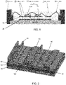
Figure 2 is a perspective view of a semiconductor die package according to this disclosure. -
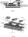
Figure 3 is a section view of a detail of the package ofFigure 2 . -
Figure 4 is an exploded view of the package ofFigure 2 - In conventional wire-bonded packages as shown in
Fig. 1 , the semiconductor components 1 (in this example, a diode and an IGBT, but these can of course be any known semiconductor components depending on the function of the device) are mounted on anupper substrate layer 10 by means of a bonding material 3, Theupper substrate layer 10 is mounted to alower substrate layer 20 via an intermediate insulating substrate layer 2. The resulting package is mounted to a base plate 4 by means of the bonding material 3. Wire bonds 5 are provided between the semiconductor components 1 and from the components 1 to connector terminals etc. and the device is mounted in a housing or case 7 made of e.g. plastic. A potting or encapsulatingmaterial 6 can be provided over the components and substrate layers to protect the device parts and provide an integral device package. The base plate acts as a heat sink and may be provided with coolant to improve thermal dissipation. For improved cooling, cooling plates can be provided on both sides of the package. In other arrangements, the components may be mounted on a bottom substrate layer and heat could be dissipated through the upper layer. Such conventional packaging structures have a high technological maturity and can be quickly and easily manufactured at low cost. As mentioned above, however, such structures are limited as regards parasitic symmetry control. The type of packaging materials used in conventional packaging are usually limited to a temperature range of around 150 to 175 deg. C. - Multilayer substrate structures in which the semiconductor components are formed in the top or bottom layer of the structure better allow components to be paralleled without the problems or parasitic asymmetries. The semiconductor layers are usually bonded to the top layer of the multilayer substrate and heat is transported through the bottom layer. A copper layer provides the electrical connections. Such structures, however, have a much higher thermal impedance than wire-bonded structures.
- The structure of the present disclosure aims to use a multilayer substrate structure to achieve the benefits of paralleling and reduced parasitic asymmetries but to retain the thermal advantages of wire-bonded structures.
- As shown in
Figs. 2 to 4 , according to the present disclosure, the semiconductor dies 30 are embedded into alayer 40 of the multilayer structure intermediate thetop 60 andbottom 70, or base plate, layer, thus reducing heat flow resistance to the bottom, heat dissipatingbase layer 70. - In the example shown. The device includes four parallel semiconductor dies 30 embedded into the
intermediate layer 40. This is just by means of example and any type of or number of dies may be provided in any desired pattern. Theintermediate layer 40 is bonded to a bottom layer orbase plate 70 e.g. by welding orsolder 45 or other bonding material or process. Atop layer 60 is mounted over theintermediate layer 40 and bonded thereto e.g. bysolder 65 or other bonding material. The layers are mounted to abase plate 70 to which they are secured by e.g. welding, solder 45 or other bonding material or process. - Other components are formed on the
top layer 60,e.g. bus bars 80,PCB 90 etc. - The
intermediate layer 40 has a sandwich structure ofceramic layers conductive layer 55. As can be best seen inFig. 3 , thecomponent 30 is embedded in the intermediate ceramic layer and is bonded to theintermediate copper layer 55. To connect the drain of the component to thepcb 90, aninterconnect 58 can be formed from the intermediate copper layer on which the component is mounted, through theceramic layer 56. The source is connected to the pcb via asource interconnect 59 directly connected to the component source. - In the preferred embodiment, these
interconnects conductive clips 100 that pass through thetop layer 60, at one end, to contact thecomponent 30 in the intermediate layer, and, at the other end, connect with devices or components on the top layer of the package such as the pcb. The use of such a clip reduces loop inductance and can also provide better thermal extraction on the top side of the package as well as at the bottom. - Although the connections between the layers may be more complex than conventional multilayer substrate structures where the components are mounted on the top layer, the use of additive manufacturing techniques can greatly simplify this and so the complexity does not provide any serious disadvantage. Subtractive manufacturing is also a possibility.
- The use of multilayer substrate design means that dies can be mounted in parallel with a high degree of symmetry which means that a greater number of devices can be utilised in the power module. The simple mounting of components such as bus bars avoids the need for complex bus bar design which would otherwise add to the overall size and weight of the package. The benefits of multilayer substrates, including increased switching speed and greater component density are thus retained whilst reducing thermal impedance compared to known multilayer designs. Therefore, additional heat conducting components are not required which would otherwise add to the size and weight of the device.
Claims (13)
- A semiconductor device package comprising a multilayer substrate including a top layer (60), a bottom layer (70) and an intermediate layer (40) between the top layer and the bottom layer, and one or more semiconductor dies (30) embedded in the intermediate layer, and further comprising conductive connector means to provide a conductive connection from the one or more dies, the conductive connector means extending through the top layer to provide connection means for one or more devices mounted on or adjacent the top layer.
- The semiconductor device package of claim 1, wherein the intermediate layer includes a ceramic layer and a conductive layer, and wherein the one or more semiconductor dies is embedded in the ceramic layer and in electrical contact with the conductive layer.
- The semiconductor device package of claim 2, wherein the conductive layer is a copper layer (55).
- The semiconductor device package of claim 1, 2 or 3, wherein the conductive connector means comprises a clip (100) of conductive material connected to the one or more semiconductor dies.
- The semiconductor device package of claim 4, wherein the clip is made of copper.
- The semiconductor device package of any preceding claim, further comprising one or more bus bar components (80) mounted on the top layer on a side away from the intermediate layer.
- The semiconductor device package of any preceding claim, further comprising one or more printed circuit boards (90) mounted on the top layer on a side away from the intermediate layer.
- The semiconductor device package of any preceding claim, comprising a plurality of semiconductor dies arranged in a parallel pattern.
- The semiconductor device package of any preceding claim, wherein the bottom layer is a heat sink.
- A method of forming a semiconductor device package comprising embedding one or more semiconductor dies in a ceramic substrate layer, providing a top substrate layer over one side of the ceramic substrate layer and a bottom substrate layer over an opposite side of the ceramic substrate layer; providing a conductive connection from the one or more dies through the top layer to provide a connection for one or more devices mounted on or adjacent the top layer.
- The method of claim 10, further comprising mounting one or more bus bar components (80) on the top layer on a side away from the intermediate layer.
- The method of claim 10 or 11, further comprising mounting one or more printed circuit boards (90) on the top layer on a side away from the intermediate layer.
- The method of any of claims 10 to 12, further comprising providing a plurality of semiconductor dies arranged in a parallel pattern.
Priority Applications (2)
| Application Number | Priority Date | Filing Date | Title |
|---|---|---|---|
| EP20216024.8A EP4016618B1 (en) | 2020-12-21 | 2020-12-21 | Power device packaging |
| US17/542,645 US11935807B2 (en) | 2020-12-21 | 2021-12-06 | Plurality of dies electrically connected to a printed circuit board by a clip |
Applications Claiming Priority (1)
| Application Number | Priority Date | Filing Date | Title |
|---|---|---|---|
| EP20216024.8A EP4016618B1 (en) | 2020-12-21 | 2020-12-21 | Power device packaging |
Publications (2)
| Publication Number | Publication Date |
|---|---|
| EP4016618A1 true EP4016618A1 (en) | 2022-06-22 |
| EP4016618B1 EP4016618B1 (en) | 2025-01-29 |
Family
ID=73856152
Family Applications (1)
| Application Number | Title | Priority Date | Filing Date |
|---|---|---|---|
| EP20216024.8A Active EP4016618B1 (en) | 2020-12-21 | 2020-12-21 | Power device packaging |
Country Status (2)
| Country | Link |
|---|---|
| US (1) | US11935807B2 (en) |
| EP (1) | EP4016618B1 (en) |
Families Citing this family (2)
| Publication number | Priority date | Publication date | Assignee | Title |
|---|---|---|---|---|
| US11817750B2 (en) * | 2021-01-14 | 2023-11-14 | GM Global Technology Operations LLC | Planar power module with high power density packaging |
| US12538428B2 (en) | 2023-01-24 | 2026-01-27 | Simmonds Precision Products, Inc. | Electrical circuit board assemblies |
Citations (8)
| Publication number | Priority date | Publication date | Assignee | Title |
|---|---|---|---|---|
| EP0597144A1 (en) * | 1992-11-12 | 1994-05-18 | IXYS Semiconductor GmbH | Hybrid power electronic device |
| US20060281297A1 (en) * | 2004-01-27 | 2006-12-14 | Nobuaki Ogawa | Multilayer electronic part and structure for mounting multilayer electronic part |
| US20100290191A1 (en) * | 2009-05-14 | 2010-11-18 | Megica Corporation | System-in packages |
| US8617927B1 (en) * | 2011-11-29 | 2013-12-31 | Hrl Laboratories, Llc | Method of mounting electronic chips |
| US20170171978A1 (en) * | 2015-12-10 | 2017-06-15 | Industrial Technology Research Institute | Power module and manufacturing method thereof |
| US10163798B1 (en) * | 2017-12-22 | 2018-12-25 | Intel Corporation | Embedded multi-die interconnect bridge packages with lithotgraphically formed bumps and methods of assembling same |
| US20190378786A1 (en) * | 2016-12-20 | 2019-12-12 | Robert Bosch Gmbh | Power module comprising a housing which is formed in levels |
| US20200235067A1 (en) * | 2019-01-22 | 2020-07-23 | Texas Instruments Incorporated | Electronic device flip chip package with exposed clip |
Family Cites Families (10)
| Publication number | Priority date | Publication date | Assignee | Title |
|---|---|---|---|---|
| TWI324901B (en) * | 2007-01-08 | 2010-05-11 | Unimicron Technology Corp | Printed circuit board structure integrating electronic components |
| US8884343B2 (en) | 2012-02-24 | 2014-11-11 | Texas Instruments Incorporated | System in package and method for manufacturing the same |
| US9437516B2 (en) * | 2014-01-07 | 2016-09-06 | Infineon Technologies Austria Ag | Chip-embedded packages with backside die connection |
| US9659854B2 (en) | 2014-04-16 | 2017-05-23 | Gan Systems Inc. | Embedded packaging for devices and systems comprising lateral GaN power transistors |
| US9701534B2 (en) | 2015-01-28 | 2017-07-11 | STATS ChipPAC Pte. Ltd. | Semiconductor device and method of forming MEMS package |
| WO2017178382A2 (en) | 2016-04-11 | 2017-10-19 | At&S Austria Technologie & Systemtechnik Aktiengesellschaft Mbh | Batch manufacture of component carriers |
| US9966371B1 (en) | 2016-11-04 | 2018-05-08 | General Electric Company | Electronics package having a multi-thickness conductor layer and method of manufacturing thereof |
| DE102017105330B4 (en) | 2017-03-14 | 2020-10-15 | Infineon Technologies Austria Ag | Power semiconductor component package and method for embedding a power semiconductor die |
| US10796998B1 (en) | 2019-04-10 | 2020-10-06 | Gan Systems Inc. | Embedded packaging for high voltage, high temperature operation of power semiconductor devices |
| IT201900006736A1 (en) * | 2019-05-10 | 2020-11-10 | Applied Materials Inc | PACKAGE MANUFACTURING PROCEDURES |
-
2020
- 2020-12-21 EP EP20216024.8A patent/EP4016618B1/en active Active
-
2021
- 2021-12-06 US US17/542,645 patent/US11935807B2/en active Active
Patent Citations (8)
| Publication number | Priority date | Publication date | Assignee | Title |
|---|---|---|---|---|
| EP0597144A1 (en) * | 1992-11-12 | 1994-05-18 | IXYS Semiconductor GmbH | Hybrid power electronic device |
| US20060281297A1 (en) * | 2004-01-27 | 2006-12-14 | Nobuaki Ogawa | Multilayer electronic part and structure for mounting multilayer electronic part |
| US20100290191A1 (en) * | 2009-05-14 | 2010-11-18 | Megica Corporation | System-in packages |
| US8617927B1 (en) * | 2011-11-29 | 2013-12-31 | Hrl Laboratories, Llc | Method of mounting electronic chips |
| US20170171978A1 (en) * | 2015-12-10 | 2017-06-15 | Industrial Technology Research Institute | Power module and manufacturing method thereof |
| US20190378786A1 (en) * | 2016-12-20 | 2019-12-12 | Robert Bosch Gmbh | Power module comprising a housing which is formed in levels |
| US10163798B1 (en) * | 2017-12-22 | 2018-12-25 | Intel Corporation | Embedded multi-die interconnect bridge packages with lithotgraphically formed bumps and methods of assembling same |
| US20200235067A1 (en) * | 2019-01-22 | 2020-07-23 | Texas Instruments Incorporated | Electronic device flip chip package with exposed clip |
Also Published As
| Publication number | Publication date |
|---|---|
| US11935807B2 (en) | 2024-03-19 |
| US20220199483A1 (en) | 2022-06-23 |
| EP4016618B1 (en) | 2025-01-29 |
Similar Documents
| Publication | Publication Date | Title |
|---|---|---|
| US10636732B2 (en) | Power module based on multi-layer circuit board | |
| US9530707B2 (en) | Semiconductor module | |
| US10658342B2 (en) | Vertically stacked multichip modules | |
| US8654541B2 (en) | Three-dimensional power electronics packages | |
| KR102586458B1 (en) | semiconductor sub-assembly and semiconductor power module | |
| US11915999B2 (en) | Semiconductor device having a carrier, semiconductor chip packages mounted on the carrier and a cooling element | |
| JP2014199829A (en) | Semiconductor module and inverter mounting the same | |
| KR102490612B1 (en) | Power semiconductor module | |
| US10888036B1 (en) | Thermal management assemblies for electronic assemblies circumferentially mounted on a motor | |
| CN112713120A (en) | Power electronic component and method for producing the same | |
| CN113823516A (en) | Solid state switchgear including heat sink and control electronics construction | |
| US11935807B2 (en) | Plurality of dies electrically connected to a printed circuit board by a clip | |
| CN119365979A (en) | Power electronic assembly with mountable power module | |
| EP3506725B1 (en) | Electronic assembly with enhanced high power density | |
| KR102829692B1 (en) | Power module and manufacturing method thereof | |
| CN101785104A (en) | Module construction and connection technology using metal stamped grids or stamped and bent parts bent out of plane | |
| US20180040562A1 (en) | Elektronisches modul und verfahren zu seiner herstellung | |
| KR102792456B1 (en) | Power module and manufacturing method thereof | |
| TW202332357A (en) | Power module | |
| US20240128197A1 (en) | Assemblies with embedded semiconductor device modules and related methods | |
| US20070145576A1 (en) | Power Semiconductor Circuit And Method Of Manufacturing A Power Semiconductor Circuit | |
| KR101897304B1 (en) | Power module | |
| CN218647940U (en) | Power module | |
| CN218647917U (en) | Power module | |
| KR102843819B1 (en) | Power module including interconnection structure using printed circuit board |
Legal Events
| Date | Code | Title | Description |
|---|---|---|---|
| PUAI | Public reference made under article 153(3) epc to a published international application that has entered the european phase |
Free format text: ORIGINAL CODE: 0009012 |
|
| STAA | Information on the status of an ep patent application or granted ep patent |
Free format text: STATUS: THE APPLICATION HAS BEEN PUBLISHED |
|
| AK | Designated contracting states |
Kind code of ref document: A1 Designated state(s): AL AT BE BG CH CY CZ DE DK EE ES FI FR GB GR HR HU IE IS IT LI LT LU LV MC MK MT NL NO PL PT RO RS SE SI SK SM TR |
|
| STAA | Information on the status of an ep patent application or granted ep patent |
Free format text: STATUS: REQUEST FOR EXAMINATION WAS MADE |
|
| 17P | Request for examination filed |
Effective date: 20221221 |
|
| RBV | Designated contracting states (corrected) |
Designated state(s): AL AT BE BG CH CY CZ DE DK EE ES FI FR GB GR HR HU IE IS IT LI LT LU LV MC MK MT NL NO PL PT RO RS SE SI SK SM TR |
|
| GRAP | Despatch of communication of intention to grant a patent |
Free format text: ORIGINAL CODE: EPIDOSNIGR1 |
|
| STAA | Information on the status of an ep patent application or granted ep patent |
Free format text: STATUS: GRANT OF PATENT IS INTENDED |
|
| INTG | Intention to grant announced |
Effective date: 20240813 |
|
| GRAS | Grant fee paid |
Free format text: ORIGINAL CODE: EPIDOSNIGR3 |
|
| GRAA | (expected) grant |
Free format text: ORIGINAL CODE: 0009210 |
|
| STAA | Information on the status of an ep patent application or granted ep patent |
Free format text: STATUS: THE PATENT HAS BEEN GRANTED |
|
| AK | Designated contracting states |
Kind code of ref document: B1 Designated state(s): AL AT BE BG CH CY CZ DE DK EE ES FI FR GB GR HR HU IE IS IT LI LT LU LV MC MK MT NL NO PL PT RO RS SE SI SK SM TR |
|
| REG | Reference to a national code |
Ref country code: GB Ref legal event code: FG4D |
|
| REG | Reference to a national code |
Ref country code: CH Ref legal event code: EP |
|
| REG | Reference to a national code |
Ref country code: DE Ref legal event code: R096 Ref document number: 602020045469 Country of ref document: DE |
|
| REG | Reference to a national code |
Ref country code: IE Ref legal event code: FG4D |
|
| REG | Reference to a national code |
Ref country code: NL Ref legal event code: MP Effective date: 20250129 |
|
| PG25 | Lapsed in a contracting state [announced via postgrant information from national office to epo] |
Ref country code: NL Free format text: LAPSE BECAUSE OF FAILURE TO SUBMIT A TRANSLATION OF THE DESCRIPTION OR TO PAY THE FEE WITHIN THE PRESCRIBED TIME-LIMIT Effective date: 20250129 |
|
| PG25 | Lapsed in a contracting state [announced via postgrant information from national office to epo] |
Ref country code: RS Free format text: LAPSE BECAUSE OF FAILURE TO SUBMIT A TRANSLATION OF THE DESCRIPTION OR TO PAY THE FEE WITHIN THE PRESCRIBED TIME-LIMIT Effective date: 20250429 |
|
| PG25 | Lapsed in a contracting state [announced via postgrant information from national office to epo] |
Ref country code: FI Free format text: LAPSE BECAUSE OF FAILURE TO SUBMIT A TRANSLATION OF THE DESCRIPTION OR TO PAY THE FEE WITHIN THE PRESCRIBED TIME-LIMIT Effective date: 20250129 |
|
| PG25 | Lapsed in a contracting state [announced via postgrant information from national office to epo] |
Ref country code: PL Free format text: LAPSE BECAUSE OF FAILURE TO SUBMIT A TRANSLATION OF THE DESCRIPTION OR TO PAY THE FEE WITHIN THE PRESCRIBED TIME-LIMIT Effective date: 20250129 |
|
| PG25 | Lapsed in a contracting state [announced via postgrant information from national office to epo] |
Ref country code: ES Free format text: LAPSE BECAUSE OF FAILURE TO SUBMIT A TRANSLATION OF THE DESCRIPTION OR TO PAY THE FEE WITHIN THE PRESCRIBED TIME-LIMIT Effective date: 20250129 |
|
| REG | Reference to a national code |
Ref country code: LT Ref legal event code: MG9D |
|
| PG25 | Lapsed in a contracting state [announced via postgrant information from national office to epo] |
Ref country code: IS Free format text: LAPSE BECAUSE OF FAILURE TO SUBMIT A TRANSLATION OF THE DESCRIPTION OR TO PAY THE FEE WITHIN THE PRESCRIBED TIME-LIMIT Effective date: 20250529 Ref country code: NO Free format text: LAPSE BECAUSE OF FAILURE TO SUBMIT A TRANSLATION OF THE DESCRIPTION OR TO PAY THE FEE WITHIN THE PRESCRIBED TIME-LIMIT Effective date: 20250429 |
|
| REG | Reference to a national code |
Ref country code: AT Ref legal event code: MK05 Ref document number: 1764354 Country of ref document: AT Kind code of ref document: T Effective date: 20250129 |
|
| PG25 | Lapsed in a contracting state [announced via postgrant information from national office to epo] |
Ref country code: HR Free format text: LAPSE BECAUSE OF FAILURE TO SUBMIT A TRANSLATION OF THE DESCRIPTION OR TO PAY THE FEE WITHIN THE PRESCRIBED TIME-LIMIT Effective date: 20250129 |
|
| PG25 | Lapsed in a contracting state [announced via postgrant information from national office to epo] |
Ref country code: PT Free format text: LAPSE BECAUSE OF FAILURE TO SUBMIT A TRANSLATION OF THE DESCRIPTION OR TO PAY THE FEE WITHIN THE PRESCRIBED TIME-LIMIT Effective date: 20250529 Ref country code: LV Free format text: LAPSE BECAUSE OF FAILURE TO SUBMIT A TRANSLATION OF THE DESCRIPTION OR TO PAY THE FEE WITHIN THE PRESCRIBED TIME-LIMIT Effective date: 20250129 |
|
| PG25 | Lapsed in a contracting state [announced via postgrant information from national office to epo] |
Ref country code: BG Free format text: LAPSE BECAUSE OF FAILURE TO SUBMIT A TRANSLATION OF THE DESCRIPTION OR TO PAY THE FEE WITHIN THE PRESCRIBED TIME-LIMIT Effective date: 20250129 Ref country code: GR Free format text: LAPSE BECAUSE OF FAILURE TO SUBMIT A TRANSLATION OF THE DESCRIPTION OR TO PAY THE FEE WITHIN THE PRESCRIBED TIME-LIMIT Effective date: 20250430 |
|
| PG25 | Lapsed in a contracting state [announced via postgrant information from national office to epo] |
Ref country code: AT Free format text: LAPSE BECAUSE OF FAILURE TO SUBMIT A TRANSLATION OF THE DESCRIPTION OR TO PAY THE FEE WITHIN THE PRESCRIBED TIME-LIMIT Effective date: 20250129 |
|
| PG25 | Lapsed in a contracting state [announced via postgrant information from national office to epo] |
Ref country code: SE Free format text: LAPSE BECAUSE OF FAILURE TO SUBMIT A TRANSLATION OF THE DESCRIPTION OR TO PAY THE FEE WITHIN THE PRESCRIBED TIME-LIMIT Effective date: 20250129 |
|
| PG25 | Lapsed in a contracting state [announced via postgrant information from national office to epo] |
Ref country code: SM Free format text: LAPSE BECAUSE OF FAILURE TO SUBMIT A TRANSLATION OF THE DESCRIPTION OR TO PAY THE FEE WITHIN THE PRESCRIBED TIME-LIMIT Effective date: 20250129 |
|
| PG25 | Lapsed in a contracting state [announced via postgrant information from national office to epo] |
Ref country code: DK Free format text: LAPSE BECAUSE OF FAILURE TO SUBMIT A TRANSLATION OF THE DESCRIPTION OR TO PAY THE FEE WITHIN THE PRESCRIBED TIME-LIMIT Effective date: 20250129 |
|
| PG25 | Lapsed in a contracting state [announced via postgrant information from national office to epo] |
Ref country code: IT Free format text: LAPSE BECAUSE OF FAILURE TO SUBMIT A TRANSLATION OF THE DESCRIPTION OR TO PAY THE FEE WITHIN THE PRESCRIBED TIME-LIMIT Effective date: 20250129 |
|
| PG25 | Lapsed in a contracting state [announced via postgrant information from national office to epo] |
Ref country code: CZ Free format text: LAPSE BECAUSE OF FAILURE TO SUBMIT A TRANSLATION OF THE DESCRIPTION OR TO PAY THE FEE WITHIN THE PRESCRIBED TIME-LIMIT Effective date: 20250129 Ref country code: EE Free format text: LAPSE BECAUSE OF FAILURE TO SUBMIT A TRANSLATION OF THE DESCRIPTION OR TO PAY THE FEE WITHIN THE PRESCRIBED TIME-LIMIT Effective date: 20250129 |
|
| PG25 | Lapsed in a contracting state [announced via postgrant information from national office to epo] |
Ref country code: RO Free format text: LAPSE BECAUSE OF FAILURE TO SUBMIT A TRANSLATION OF THE DESCRIPTION OR TO PAY THE FEE WITHIN THE PRESCRIBED TIME-LIMIT Effective date: 20250129 |
|
| PG25 | Lapsed in a contracting state [announced via postgrant information from national office to epo] |
Ref country code: SK Free format text: LAPSE BECAUSE OF FAILURE TO SUBMIT A TRANSLATION OF THE DESCRIPTION OR TO PAY THE FEE WITHIN THE PRESCRIBED TIME-LIMIT Effective date: 20250129 |
|
| REG | Reference to a national code |
Ref country code: DE Ref legal event code: R097 Ref document number: 602020045469 Country of ref document: DE |
|
| REG | Reference to a national code |
Ref country code: DE Ref legal event code: R079 Ref document number: 602020045469 Country of ref document: DE Free format text: PREVIOUS MAIN CLASS: H01L0023538000 Ipc: H10W0070600000 |
|
| PLBE | No opposition filed within time limit |
Free format text: ORIGINAL CODE: 0009261 |
|
| STAA | Information on the status of an ep patent application or granted ep patent |
Free format text: STATUS: NO OPPOSITION FILED WITHIN TIME LIMIT |
|
| 26N | No opposition filed |
Effective date: 20251030 |
|
| PGFP | Annual fee paid to national office [announced via postgrant information from national office to epo] |
Ref country code: DE Payment date: 20251126 Year of fee payment: 6 |
|
| PGFP | Annual fee paid to national office [announced via postgrant information from national office to epo] |
Ref country code: GB Payment date: 20251119 Year of fee payment: 6 |
|
| PGFP | Annual fee paid to national office [announced via postgrant information from national office to epo] |
Ref country code: FR Payment date: 20251119 Year of fee payment: 6 |