EP4016585A1 - Dispositif électronique en carbure de silicium et son procédé de fabrication - Google Patents
Dispositif électronique en carbure de silicium et son procédé de fabrication Download PDFInfo
- Publication number
- EP4016585A1 EP4016585A1 EP21212659.3A EP21212659A EP4016585A1 EP 4016585 A1 EP4016585 A1 EP 4016585A1 EP 21212659 A EP21212659 A EP 21212659A EP 4016585 A1 EP4016585 A1 EP 4016585A1
- Authority
- EP
- European Patent Office
- Prior art keywords
- layer
- face
- sic
- plane
- support substrate
- Prior art date
- Legal status (The legal status is an assumption and is not a legal conclusion. Google has not performed a legal analysis and makes no representation as to the accuracy of the status listed.)
- Granted
Links
Images



Classifications
-
- H—ELECTRICITY
- H10—SEMICONDUCTOR DEVICES; ELECTRIC SOLID-STATE DEVICES NOT OTHERWISE PROVIDED FOR
- H10P—GENERIC PROCESSES OR APPARATUS FOR THE MANUFACTURE OR TREATMENT OF DEVICES COVERED BY CLASS H10
- H10P90/00—Preparation of wafers not covered by a single main group of this subclass, e.g. wafer reinforcement
-
- H—ELECTRICITY
- H10—SEMICONDUCTOR DEVICES; ELECTRIC SOLID-STATE DEVICES NOT OTHERWISE PROVIDED FOR
- H10D—INORGANIC ELECTRIC SEMICONDUCTOR DEVICES
- H10D62/00—Semiconductor bodies, or regions thereof, of devices having potential barriers
- H10D62/40—Crystalline structures
-
- H—ELECTRICITY
- H10—SEMICONDUCTOR DEVICES; ELECTRIC SOLID-STATE DEVICES NOT OTHERWISE PROVIDED FOR
- H10P—GENERIC PROCESSES OR APPARATUS FOR THE MANUFACTURE OR TREATMENT OF DEVICES COVERED BY CLASS H10
- H10P10/00—Bonding of wafers, substrates or parts of devices
- H10P10/12—Bonding of semiconductor wafers or semiconductor substrates to semiconductor wafers or semiconductor substrates
- H10P10/128—Bonding of semiconductor wafers or semiconductor substrates to semiconductor wafers or semiconductor substrates by direct semiconductor to semiconductor bonding
-
- H—ELECTRICITY
- H10—SEMICONDUCTOR DEVICES; ELECTRIC SOLID-STATE DEVICES NOT OTHERWISE PROVIDED FOR
- H10P—GENERIC PROCESSES OR APPARATUS FOR THE MANUFACTURE OR TREATMENT OF DEVICES COVERED BY CLASS H10
- H10P14/00—Formation of materials, e.g. in the shape of layers or pillars
- H10P14/20—Formation of materials, e.g. in the shape of layers or pillars of semiconductor materials
- H10P14/29—Formation of materials, e.g. in the shape of layers or pillars of semiconductor materials characterised by the substrates
- H10P14/2901—Materials
- H10P14/2902—Materials being Group IVA materials
- H10P14/2904—Silicon carbide
-
- H—ELECTRICITY
- H10—SEMICONDUCTOR DEVICES; ELECTRIC SOLID-STATE DEVICES NOT OTHERWISE PROVIDED FOR
- H10P—GENERIC PROCESSES OR APPARATUS FOR THE MANUFACTURE OR TREATMENT OF DEVICES COVERED BY CLASS H10
- H10P14/00—Formation of materials, e.g. in the shape of layers or pillars
- H10P14/20—Formation of materials, e.g. in the shape of layers or pillars of semiconductor materials
- H10P14/29—Formation of materials, e.g. in the shape of layers or pillars of semiconductor materials characterised by the substrates
- H10P14/2926—Crystal orientations
-
- H—ELECTRICITY
- H10—SEMICONDUCTOR DEVICES; ELECTRIC SOLID-STATE DEVICES NOT OTHERWISE PROVIDED FOR
- H10P—GENERIC PROCESSES OR APPARATUS FOR THE MANUFACTURE OR TREATMENT OF DEVICES COVERED BY CLASS H10
- H10P14/00—Formation of materials, e.g. in the shape of layers or pillars
- H10P14/20—Formation of materials, e.g. in the shape of layers or pillars of semiconductor materials
- H10P14/32—Formation of materials, e.g. in the shape of layers or pillars of semiconductor materials characterised by intermediate layers between substrates and deposited layers
- H10P14/3202—Materials thereof
- H10P14/3204—Materials thereof being Group IVA semiconducting materials
- H10P14/3208—Silicon carbide
-
- H—ELECTRICITY
- H10—SEMICONDUCTOR DEVICES; ELECTRIC SOLID-STATE DEVICES NOT OTHERWISE PROVIDED FOR
- H10P—GENERIC PROCESSES OR APPARATUS FOR THE MANUFACTURE OR TREATMENT OF DEVICES COVERED BY CLASS H10
- H10P14/00—Formation of materials, e.g. in the shape of layers or pillars
- H10P14/20—Formation of materials, e.g. in the shape of layers or pillars of semiconductor materials
- H10P14/32—Formation of materials, e.g. in the shape of layers or pillars of semiconductor materials characterised by intermediate layers between substrates and deposited layers
- H10P14/3258—Crystal orientation
-
- H—ELECTRICITY
- H10—SEMICONDUCTOR DEVICES; ELECTRIC SOLID-STATE DEVICES NOT OTHERWISE PROVIDED FOR
- H10P—GENERIC PROCESSES OR APPARATUS FOR THE MANUFACTURE OR TREATMENT OF DEVICES COVERED BY CLASS H10
- H10P14/00—Formation of materials, e.g. in the shape of layers or pillars
- H10P14/20—Formation of materials, e.g. in the shape of layers or pillars of semiconductor materials
- H10P14/34—Deposited materials, e.g. layers
- H10P14/3402—Deposited materials, e.g. layers characterised by the chemical composition
- H10P14/3404—Deposited materials, e.g. layers characterised by the chemical composition being Group IVA materials
- H10P14/3408—Silicon carbide
-
- H—ELECTRICITY
- H10—SEMICONDUCTOR DEVICES; ELECTRIC SOLID-STATE DEVICES NOT OTHERWISE PROVIDED FOR
- H10P—GENERIC PROCESSES OR APPARATUS FOR THE MANUFACTURE OR TREATMENT OF DEVICES COVERED BY CLASS H10
- H10P14/00—Formation of materials, e.g. in the shape of layers or pillars
- H10P14/20—Formation of materials, e.g. in the shape of layers or pillars of semiconductor materials
- H10P14/34—Deposited materials, e.g. layers
- H10P14/3466—Crystal orientation
-
- H—ELECTRICITY
- H10—SEMICONDUCTOR DEVICES; ELECTRIC SOLID-STATE DEVICES NOT OTHERWISE PROVIDED FOR
- H10D—INORGANIC ELECTRIC SEMICONDUCTOR DEVICES
- H10D62/00—Semiconductor bodies, or regions thereof, of devices having potential barriers
- H10D62/80—Semiconductor bodies, or regions thereof, of devices having potential barriers characterised by the materials
- H10D62/83—Semiconductor bodies, or regions thereof, of devices having potential barriers characterised by the materials being Group IV materials, e.g. B-doped Si or undoped Ge
- H10D62/832—Semiconductor bodies, or regions thereof, of devices having potential barriers characterised by the materials being Group IV materials, e.g. B-doped Si or undoped Ge being Group IV materials comprising two or more elements, e.g. SiGe
- H10D62/8325—Silicon carbide
Definitions
- the present description relates generally to electronic devices made of carbon silicide and their method of manufacture.
- the present description relates in particular to monocrystalline substrates or monocrystalline layers of carbon silicide (SiC) used, for example, for producing electronic power components.
- the SiC crystal contains numerous extended defects, in particular basal plane dislocations (BPD, English acronym for Basal Plane Dislocation), edge-type dislocations (TED, English acronym for Threading Edge Dislocation), dislocations screw type (TSD, English acronym for Threading Screw Dislocation), microholes (MP, English acronym for Micropipe), and stacking faults (SF, English acronym for Stacking Fault).
- BPD basal plane dislocations
- TED edge-type dislocations
- TSD dislocations screw type
- MP English acronym for Threading Screw Dislocation
- microholes MP, English acronym for Micropipe
- SF English acronym for Stacking Fault
- the defects with the most negative impact on the electrical performance of electronic devices using single crystal SiC substrates are TSDs, MPs, BPDs and SFs.
- manufacturers of monocrystalline SiC substrates have managed to reduce the density
- the manufacture of a monocrystalline SiC substrate having a density of extended defects, and in particular a density of BPDs, of less than 1000 defects/cm 2 has a high cost.
- a thin layer of monocrystalline SiC instead of a thick substrate of monocrystalline SiC, the thin layer being maintained on a support substrate. lower manufacturing cost.
- the SiC support advantageously having the same coefficient of expansion as the thin SiC layer.
- steps with a high thermal budget annealing and/or epitaxial growth of SiC from the thin layer, etc.
- One embodiment overcomes all or part of the drawbacks of known SiC electronic devices made from a thin layer of SiC transferred onto a low-cost substrate.
- the electronic device has a reduced manufacturing cost.
- One embodiment provides an electronic device comprising a stack of a monocrystalline SiC support substrate having a first face and a monocrystalline SiC layer comprising a second face facing the first face.
- the first face corresponds to a (11-20) plane of the SiC monocrystal of the support substrate and the second face corresponds to a plane inclined at least 1° with respect to the (11-20) plane of the SiC monocrystal of the layer. .
- the support substrate has a density of extended defects greater than 1000 BPD defects/cm 2 .
- the layer has a defect density of less than 250 BPD defects/cm 2 .
- the second face is in mechanical contact, also called physical contact, with the first face.
- the device comprises at least one electronic component formed at least by processing the layer.
- One embodiment also provides a method of manufacturing an electronic device comprising providing a single crystal SiC support substrate having a first side, forming a single crystal SiC layer attached to the support substrate, the layer including a second face facing the first face, the first face corresponding to a plane (11-20) of the SiC monocrystal of the support substrate and the second face corresponding to a plane inclined at least 1° with respect to the plane (11-20) of the SiC single crystal of the layer.
- the method comprises the formation of said layer from a monocrystalline SiC substrate.
- the method comprises the epitaxial growth of monocrystalline SiC on said substrate.
- the method comprises the formation of a weakened zone in the substrate according to a plane and the separation of the substrate according to said plane into two parts, one of which corresponds to a layer fixed to said support substrate.
- the method comprises the epitaxial growth of monocrystalline SiC on said layer.
- the defect density of an SiC monocrystal designates the BPD defect density.
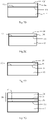
- the figure 1 is a partial schematic sectional view of an electronic device 10.
- the electronic device 10 may optionally comprise at least one electronic component, represented very schematically by a zone 26 of square shape in figure 1 .
- Electronic component 26 may be formed in layer 20 and/or on layer 20.
- Electronic component 26 may extend over the entire thickness of layer 20 and/or over the entire thickness of support substrate 12, in particular in the case of a power electronic component.
- the electronic device 10 can comprise a support, not shown, on which the support substrate 12 is fixed, on the side of the lower face 16.
- the support substrate 12 is made of monocrystalline SiC. According to one embodiment, the support substrate 12 is of the 4H polytype, which has a hexagonal crystalline system. As a variant, the support substrate 12 is of the 6H polytype, or of another polytype.
- the BPD density of the support substrate 12 is greater than 1000 defects/cm 2 , preferably greater than 1500 defects/cm 2 , more preferably greater than 3000 defects/cm 2 .
- faces 14 and 16 are substantially flat. Preferably, faces 14 and 16 are parallel.
- the upper face 14 corresponds to a basal plane of the crystal, that is to say to a crystallographic plane (11-20).
- the thickness of the support substrate 12 is between 300 ⁇ m and 1000 ⁇ m, before a possible thinning step. After a thinning step, the thickness of the support substrate 12 can be reduced down to typically 150 ⁇ m. Support substrate 12 may be doped.
- Layer 20 is made of monocrystalline SiC.
- the BPD density of layer 20 is less than 1000 defects/cm 2 , preferably less than 500 defects/cm 2 , more preferably less than 250 defects/cm 2 , even more preferably less than 100 defects/cm 2 .
- face 22 is substantially planar.
- face 24 is substantially planar.
- the faces 22 and 24 are parallel.
- the upper face 24 corresponds to a plane forming an angle, with respect to the plane (11-20) of the crystal, between 1° and 10°, preferably between 2° and 8°, in particular equal to around 4°.
- the thickness of layer 20 is between 100 nm and 15 ⁇ m.
- Layer 20 can be doped.
- the concentration of dopants in layer 20 may not be homogeneous.
- the layer 20 can comprise a stack of at least first and second single-crystal SiC sub-layers, interconnected by an epitaxial relationship, with different concentrations of dopants.
- layer 20 may comprise a homogeneous BPD density.
- the layer 20 can comprise a stack of at least first and second monocrystalline SiC sub-layers, interconnected by an epitaxial relationship, the first sub-layer being located on the side of the support substrate 12, the BPD density of the second sublayer being lower than the BPD density of the first sublayer.
- the BPD density of the first sub-layer can be between 100 defects/cm 2 and 500 defects/cm 2
- the BPD density of the second sub-layer 38 can be less than 50 defects/cm 2 .
- the electronic component 26 can be intended for microwave, high temperature and/or high voltage operation. By way of example, it may correspond to a Schottky diode, a JFET transistor, a MOSFET transistor, a bipolar transistor or a thyristor.
- the electronic component 26 can be formed by processing the layer 20 and possibly the support substrate 12.
- Structure 28 may correspond to an insulating layer. As a variant, it may comprise a stack of insulating layers between and through which conductive tracks and conductive vias extend.
- FIGS. 2A to 2G are sectional, partial and schematic views of structures obtained at successive stages of an embodiment of a method of manufacture of the electronic device 10 shown in figure 1 .
- the figure 2A represents a monocrystalline SiC substrate 30 having an upper face 32.
- the BPD density of the substrate 30 is less than 1000 defects/cm 2 , preferably less than 500 defects/cm 2 , more preferably less than 250 or even 100 defects/cm 2 .
- the upper face 32 substantially corresponds to a plane which has a cutting angle. The cut angle is defined as the angle between the free mean surface of the single crystal and a dense crystallographic plane of the single crystal. In the case of hexagonal SiC, the dense crystallographic plane is the (11-20) plane.
- the upper face 32 has a cutting angle with respect to the plane (11-20) comprised between 1° and 10°, preferably between 2° and 8°, in particular equal to about 4°.
- the figure 2B represents the structure obtained after an ion implantation step on the side of the upper face 32, which leads to the formation of a fragile zone 34 buried substantially flat in the substrate 30, delimiting with the upper face 32 a thin layer 36 which goes be transferred as described in more detail below.
- Layer 36 is intended to be part of layer 20 previously described, as will be described in more detail below.
- the transfer or transfer process known as “Smart Cut TM ” is widely known from the literature.
- the ion implantation step can be a step of implantation of light species, for example hydrogen, helium or a combination of these two species. Adjusting the implantation energy makes it possible to vary the implantation depth, that is to say the distance between the plane 34 and the upper face 32.
- the implantation energies can be between 40 keV and 200 keV.
- the doses used can be between 10 16 /cm 2 and 10 17 /cm 2 .
- the ion implantation can be carried out at a temperature below 500° C., in particular at ambient temperature.
- the plane 34 is substantially parallel to the face 32 and therefore has an angle with respect to the (11-20) plane of the SiC crystal of between 1° and 10°, preferably between 2° and 8°, in particular equal to around 4 °.
- layer 20 can be formed using other known thin layer transfer techniques.
- the Fig. 2C represents the structure obtained after a step of assembling the substrate 30 on the support substrate 12, and more precisely the face 32 of the substrate 30 on the face 14 of the support substrate 12.
- the bonding of the substrate 30 to the support substrate 12 is a direct bonding, that is to say without adding a bonding material between the substrate 30 and the support substrate 12. It can comprise the formation of a layer on the face 32 of the substrate 30 and / or on the face 14 of the support substrate 12 to facilitate the assembly of the substrate 30 with the support substrate 12, this layer possibly being a metallic layer, for example of tungsten (W), a semiconductor layer, for example of silicon (Si ) or in amorphous SiC.
- W tungsten
- Si silicon
- the bonding step by direct bonding consists in bringing face 32 of substrate 30 into contact against face 14 of support substrate 12, which results in molecular bonding of substrate 30 on support substrate 12.
- This bonding can be carried out in an atmosphere ambient, or under a controlled atmosphere and in particular under a high vacuum, of the order of 10 -6 Pa or less. It can be carried out at room temperature or at higher temperature, assisted or not by compression. Thermal annealing is generally carried out to consolidate the bond.
- the 2D figure represents the structure after a step of separating the substrate 30 at the level of the buried fragile plane 34 in two parts, layer 36 remaining attached to support substrate 12.
- the thickness of layer 36 is for example between 100 nm and 1.5 ⁇ m.
- the separation step may comprise a sufficient input of energy to separate the substrate 30 into two parts at the level of the plane 34.
- the energy input may comprise a thermal energy input, for example by annealing or sweeping laser, or a supply of mechanical energy or even a combination of thermal and mechanical stresses.
- the structure obtained therefore comprises a layer 36 of monocrystalline SiC comprising a low density of BPD (less than 1000 defects/cm 2 , preferably less than 500 defects/cm 2 , more preferably less than 100 defects/cm 2 ), on a substrate low-cost support 12 comprising a higher density of BPD (greater than 1000 defects/cm 2 and preferably greater than 1500 or even 3000 defects/cm 2 ).
- BPD low density of BPD
- the BPDs of the support substrate 12 have been blocked in the basal plane of the face 14 and do not have not emerged in layer 36, which therefore remains of very good quality.
- the exposed face of the layer 36 which corresponds substantially to the plane 34, has a cutting angle with respect to the plane (11-20) of the SiC crystal of between 1° and 10°, preferably between 2° and 8°, in particular equal to about 4°.
- the figure 2E represents the structure obtained after cleaning, polishing, smoothing or etching steps of the face 34 of the layer 36. This can cause a thinning of the layer 36, the free face 34 obtained after this polishing step always having a angle of cut relative to the plane (11-20) of the SiC crystal included between 1° and 10°, preferably between 2° and 8°, in particular equal to approximately 4°.
- the figure 2F represents the structure obtained after a thermal annealing step, for example at a temperature greater than 1500° C., for example approximately 1700° C., for a time greater than 10 minutes, for example for approximately 30 minutes.
- a thermal annealing step for example at a temperature greater than 1500° C., for example approximately 1700° C., for a time greater than 10 minutes, for example for approximately 30 minutes.
- the BPDs of the support substrate 12 are blocked in the basal plane of the face 14 and do not emerge in the layer 36.
- the steps described above in relation to the figures 2E and 2F make it possible to substantially eliminate all the defects induced during ion implantation.
- the figure 2G represents the structure obtained after a growth step of a layer 38 of monocrystalline SiC by epitaxy on layer 36 from face 34.
- Layer 38 may have a different doping from layer 36. It may have a defect density lower than the defect density of layer 36.
- This step makes it possible to produce layer 38 with a lower BPD density, of the order of 10 times to 100 times lower than the BPD density of layer 36.
- BPDs are transformed into TED during the epitaxy step by adequately controlling the growth parameters during the epitaxy step, in particular the growth rate or else the C/S ratio.
- TEDs are faults that have little or no impact on electrical devices unlike the BPD.
- the layer 38 of epitaxial SiC can comprise a BPD density of less than 50 defects/cm 2 .
- the set of layers 36 and 38 then forms the SiC layer 20 previously described in relation to the figure 1 .
- This layer 20 advantageously has a thickness greater than 3 ⁇ m, typically of the order of 5 to 15 ⁇ m, or even more to allow in particular the production of power components.
- the upper face 34 of the layer 36 having an angle relative to the plane (11-20) of the SiC crystal between 1° and 10°, preferably between 2° and 8°, in particular equal to about 4°, the growth by epitaxy of the layer 38 can be carried out by processes compatible with industrial exploitation.
- the epitaxial growth on a free face of the SiC crystal having an angle relative to the plane (11-20) of the SiC crystal of less than 1° can hardly be achieved by methods compatible with industrial exploitation.
- the BPDs of the support substrate 12 are blocked in the basal plane of the face 14 and do not emerge in the layer 20, which therefore remains of very good quality.
- layer 38 is not present.
- Layer 36 then corresponds to layer 20 previously described in relation to the figure 1 . It can be directly processed to make components.
- the method may comprise subsequent steps of forming electronic components, in particular at the level of the layer 20 and materialized on the figure 1 through area 26 and forming interconnect/cladding structure 28 previously described in connection with the figure 1 .
- the BPDs of the support substrate 12 are also blocked in the plane (11-20) of the face 14 and do not emerge through the layer 20.
- These subsequent steps may further comprise the thinning of the support substrate 12, for example by polishing, grinding, and/or chemical etching. These subsequent steps can include the formation of the metal tracks 18.
- several copies of the electronic device 10 can be made in and on the layer 20.
- a step of separating the electronic devices can then be provided, for example by sawing.
- FIGS. 3A to 3D are partial and schematic cross-sectional views of structures obtained at successive stages of another embodiment of a method for manufacturing the electronic device 10 shown in figure 1 .
- the Figure 3A represents the structure obtained after a step of growth of a layer 40 of SiC by epitaxy on the substrate 30 of SiC from the face 32.
- the substrate 30 has good crystalline quality with few defects, the BPD density of substrate 30 being less than 1000 defects/cm 2 , preferably less than 500 defects/cm 2 , more preferably less than 250 or even 100 defects/cm 2 .
- the layer 40 can have the same doping or a different doping of the substrate 30 of SiC. This step makes it possible to produce the layer 40 with a lower BPD density, preferably 10 times lower, more preferably 100 times lower, than the BPD density of the substrate 30.
- the Figure 3B represents the structure obtained after an implantation step which leads to the formation of a fragile buried plane 34 in the layer 40, delimiting, with the free face 42 of the layer 40, a thin layer 44 intended to be transferred as is described in detail later.
- the implantation step can be implemented as described above in relation to the figure 2B .
- the Fig. 3C represents the structure obtained after a step of bonding layer 40 to support substrate 12, and more precisely of the face 42 of the layer 40 on the face 14 of the support substrate 12.
- the bonding step can be implemented as described above in relation to the Fig. 2C .
- the 3d figure represents the structure obtained after a step of separating the layer 40 at the level of the buried fragile plane 34 into two parts, the layer 44 remaining fixed to the support substrate 12.
- the separation step can be implemented as described previously in relation to the 2D figure .
- the structure obtained therefore comprises a layer 44 of monocrystalline SiC comprising a low BPD density (less than 500 defects/cm 2 , preferably less than 250 defects/cm 2 , more preferably less than 100 defects/cm 2 ) on a support substrate 12 at low cost having a higher density of BPD.
- the exposed face of layer 44 which substantially corresponds to plane 34, has a cut angle with respect to the basal plane of the SiC between 1° and 10°, preferably between 2° and 8°, in particular around 4°.
- the BPD density in this layer will be further reduced, by a factor of the order of 10 to 100 with respect to the layer 44.
- a BPD density of less than 50 defects/cm 2 preferably less than 20 defects/cm 2 , more preferably less than 10 defects/cm 2 .
- FIGS. 4A to 4D are partial and schematic cross-sectional views of structures obtained at successive stages of another embodiment of a method for manufacturing the electronic device 10 shown in figure 1 for which the sampling of the monocrystalline film is carried out by a peeling technique (spalling in English).
- the figure 4A represents the structure obtained after a step of depositing a highly strained layer 48, for example of nitride on the upper face 32 of the substrate 30 and a step of applying an adhesive strip 50 to the surface of the strained layer 48.
- the figure 4B represents the structure obtained after a step of separation by peeling of a layer 52 of the substrate 30 secured to the constrained layer 48 which remains attached to the adhesive strip 50.
- the layer 52 has a free face 54 on the side opposite the adhesive strip 50
- the thickness of layer 52 can be between 100 nm and 1.5 ⁇ m.
- the Fig. 4C represents the structure obtained after a step of adhesion of the layer 52 on the support substrate 12, and more precisely of the face 54 of the layer 52 on the face 14 of the support substrate 12.
- the bonding step can be implemented as previously described in connection with the Fig. 2C after a suitable surface treatment of the face 54, and in particular mechanical-chemical polishing, to make it compatible with this bonding. Indeed, the face 54 is very rough after peeling.
- the 4D figure represents the structure obtained after the removal of the adhesive strip 50 then the removal of the constrained layer 48, for example by selective etching.
Landscapes
- Crystals, And After-Treatments Of Crystals (AREA)
- Carbon And Carbon Compounds (AREA)
- Recrystallisation Techniques (AREA)
- Chemical & Material Sciences (AREA)
- Crystallography & Structural Chemistry (AREA)
Abstract
Description
- La présente description concerne de façon générale les dispositifs électroniques en siliciure de carbone et leur procédé de fabrication.
- La présente description porte notamment sur des substrats monocristallins ou des couches monocristallines de siliciure de carbone (SiC) utilisés, par exemple, pour la réalisation de composants électroniques de puissance. Le cristal SiC comporte de nombreux défauts étendus (en anglais extended defects), notamment des dislocations de plan basal (BPD, sigle anglais pour Basal Plane Dislocation), des dislocations de type coin (TED, sigle anglais pour Threading Edge Dislocation), des dislocations de type vis (TSD, sigle anglais pour Threading Screw Dislocation), des microtrous (MP, sigle anglais pour Micropipe), et des fautes d'empilement (SF, sigle anglais pour Stacking Fault). Les défauts ayant l'impact le plus négatif sur les performances électriques des dispositifs électroniques utilisant des substrats monocristallins en SiC sont les TSD, les MP, les BPD et les SF. Aujourd'hui, les fabricants de substrats en SiC monocristallins sont parvenus à réduire la densité de TSD et de MP de sorte que ces défauts n'ont plus d'impact significatif sur les performances électriques des composants électroniques réalisés avec ces substrats. Les défauts BPD sont maintenant pénalisants.
- La fabrication d'un substrat monocristallin en SiC ayant une densité de défauts étendus, et notamment une densité de BPD, inférieure à 1000 défauts/cm2 présente un coût élevé. Pour réduire les coûts de fabrication d'un dispositif électronique utilisant un tel substrat en SiC, il est connu d'utiliser une couche fine de SiC monocristallin au lieu d'un substrat épais de SiC monocristallin, la couche fine étant maintenue sur un substrat support de coût de fabrication plus faible.
- En particulier, il est connu de reporter une fine couche de SiC monocristallin ayant une faible densité de défauts sur un support en SiC monocristallin ayant une densité élevée de défauts, le support en SiC ayant avantageusement le même coefficient de dilatation que la couche fine de SiC. Toutefois, lors des étapes ultérieures du procédé de fabrication du dispositif électronique, qui comprennent généralement des étapes à fort budget thermique (recuit et/ou croissance épitaxiale de SiC depuis la couche fine, ...), on peut observer la propagation de défauts du support dans le reste du dispositif électronique, ce qui n'est pas souhaitable.
- Un mode de réalisation pallie tout ou partie des inconvénients des dispositifs électroniques en SiC connus réalisés à partir d'une fine couche de SiC reportée sur un substrat bas coût.
- Selon un mode de réalisation, le dispositif électronique a un coût de fabrication réduit.
- Un mode de réalisation prévoit un dispositif électronique comprenant un empilement d'un substrat support en SiC monocristallin ayant une première face et d'une couche en SiC monocristallin comprenant une deuxième face en vis-à-vis de la première face. La première face correspond à un plan (11-20) du monocristal de SiC du substrat support et la deuxième face correspond à un plan incliné d'au moins 1 ° par rapport au plan (11-20) du monocristal de SiC de la couche.
- Selon un mode de réalisation, le substrat support a une densité de défauts étendus supérieure à 1000 défauts BPD/cm2.
- Selon un mode de réalisation, la couche a une densité de défauts inférieure à 250 défauts BPD/cm2.
- Selon un mode de réalisation, la deuxième face est en contact mécanique, également appelé contact physique, avec la première face.
- Selon un mode de réalisation, le dispositif comprend au moins un composant électronique formé au moins par traitement de la couche.
- Un mode de réalisation prévoit également un procédé de fabrication d'un dispositif électronique comprenant la fourniture d'un substrat support en SiC monocristallin ayant une première face, la formation d'une couche en SiC monocristallin fixé au substrat support, la couche comprenant une deuxième face en vis-à-vis de la première face, la première face correspondant à un plan (11-20) du monocristal de SiC du substrat support et la deuxième face correspondant à un plan incliné d'au moins 1 ° par rapport au plan (11-20) du monocristal de SiC de la couche.
- Selon un mode de réalisation, le procédé comprend la formation de ladite couche à partir d'un substrat en SiC monocristallin.
- Selon un mode de réalisation, le procédé comprend la croissance épitaxiale de SiC monocristallin sur ledit substrat.
- Selon un mode de réalisation, le procédé comprend la formation d'une zone fragilisée dans le substrat selon un plan et la séparation du substrat selon ledit plan en deux parties dont l'une correspond à une couche fixée audit substrat support.
- Selon un mode de réalisation, le procédé comprend la croissance épitaxiale de SiC monocristallin sur ladite couche.
- Ces caractéristiques et avantages, ainsi que d'autres, seront exposés en détail dans la description suivante de modes de réalisation particuliers faite à titre non limitatif en relation avec les figures jointes parmi lesquelles :
- la
figure 1 est une vue en coupe, partielle et schématique, d'un mode de réalisation d'un dispositif électronique ; - la
figure 2A illustre une étape d'un mode de réalisation d'un procédé de fabrication du dispositif électronique de lafigure 1 ; - la
figure 2B illustre une autre étape du procédé ; - la
figure 2C illustre une autre étape du procédé ; - la
figure 2D illustre une autre étape du procédé ; - la
figure 2E illustre une autre étape du procédé ; - la
figure 2F illustre une autre étape du procédé ; - la
figure 2G illustre une autre étape du procédé ; - la
figure 3A illustre une étape d'un autre mode de réalisation d'un procédé de fabrication du dispositif électronique de lafigure 1 ; - la
figure 3B illustre une autre étape du procédé ; - la
figure 3C illustre une autre étape du procédé ; - la
figure 3D illustre une autre étape du procédé ; - la
figure 4A illustre une étape d'un autre mode de réalisation d'un procédé de fabrication du dispositif électronique de lafigure 1 ; - la
figure 4B illustre une autre étape du procédé ; - la
figure 4C illustre une autre étape du procédé ; et - la
figure 4D illustre une autre étape du procédé. - De mêmes éléments ont été désignés par de mêmes références dans les différentes figures. En particulier, les éléments structurels et/ou fonctionnels communs aux différents modes de réalisation peuvent présenter les mêmes références et peuvent disposer de propriétés structurelles, dimensionnelles et matérielles identiques. Par souci de clarté, seuls les étapes et éléments utiles à la compréhension des modes de réalisation décrits ont été représentés et sont détaillés. En particulier, les étapes de fabrication de composants électroniques sur et/ou dans un substrat de SiC sont bien connus de l'homme du métier et ne sont pas décrits en détail.
- Sauf précision contraire, lorsque l'on fait référence à deux éléments connectés entre eux, cela signifie directement connectés sans éléments intermédiaires autres que des conducteurs, et lorsque l'on fait référence à deux éléments reliés (en anglais "coupled") entre eux, cela signifie que ces deux éléments peuvent être connectés ou être reliés par l'intermédiaire d'un ou plusieurs autres éléments.
- Dans la description qui suit, lorsque l'on fait référence à des qualificatifs de position absolue, tels que les termes "avant", "arrière", "haut", "bas", "gauche", "droite", etc., ou relative, tels que les termes "dessus", "dessous", "supérieur", "inférieur", etc., ou à des qualificatifs d'orientation, tels que les termes "horizontal", "vertical", etc., il est fait référence sauf précision contraire à l'orientation des figures ou à un dispositif électronique dans une position normale d'utilisation. Sauf précision contraire, les expressions "environ", "approximativement", "sensiblement", et "de l'ordre de" signifient à 10 % près, de préférence à 5 % près. En outre, on considère ici que les termes "isolant" et "conducteur" signifient respectivement "isolant électriquement" et "conducteur électriquement".
- Dans la suite de la description, la densité de défaut d'un monocristal SiC désigne la densité de défauts BPD.
- La
figure 1 est une vue en coupe, partielle et schématique, d'un dispositif électronique 10. - Le dispositif électronique 10 comprend :
- un substrat support 12 en SiC monocristallin avec une première densité de défauts, ayant une face supérieure 14 et une face inférieure 16, opposée à la face supérieure 14 ;
- éventuellement au moins une piste métallique 18 au contact de la face inférieure 16 du substrat support 12 ;
- une couche 20 en SiC monocristallin avec une deuxième densité de défauts inférieure à la première densité de défauts, la couche 20 ayant une face inférieure 22 reposant sur la face 14 et au contact du substrat support 12, et une face supérieure 24 du côté opposé au substrat support 12 ; et
- une structure 28 d'interconnexion et/ou de revêtement recouvrant la couche 20 du côté de la face 24.
- Le dispositif électronique 10 peut éventuellement comprendre au moins un composant électronique, représenté très schématiquement par une zone 26 de forme carrée en
figure 1 . Le composant électronique 26 peut être formé dans la couche 20 et/ou sur la couche 20. Le composant électronique 26 peut s'étendre sur toute l'épaisseur de la couche 20 et/ou sur toute l'épaisseur du substrat support 12, notamment dans le cas d'un composant électronique de puissance. - Selon une variante, le dispositif électronique 10 peut comprendre un support, non représenté, sur lequel est fixé le substrat support 12, du côté de la face inférieure 16.
- Le substrat support 12 est en SiC monocristallin. Selon un mode de réalisation, le substrat support 12 est du polytype 4H, qui présente un système cristallin hexagonal. A titre de variante, le substrat support 12 est du polytype 6H, ou d'un autre polytype. La densité de BPD du substrat support 12 est supérieure à 1000 défauts/cm2, de préférence supérieure à 1500 défauts/cm2, plus préférentiellement supérieure à 3000 défauts/cm2. Selon un mode de réalisation, les faces 14 et 16 sont sensiblement planes. De préférence, les faces 14 et 16 sont parallèles. La face supérieure 14 correspond à un plan basal du cristal, c'est-à-dire à un plan cristallographique (11-20). L'épaisseur du substrat support 12 est comprise entre 300 µm et 1000 µm, avant une éventuelle étape d'amincissement. Après une étape d'amincissement, l'épaisseur du substrat support 12 peut être réduite jusqu'à typiquement 150 µm. Le substrat support 12 peut être dopé.
- La couche 20 est en SiC monocristallin. La densité de BPD de la couche 20 est inférieure à 1000 défauts/cm2, de préférence inférieure à 500 défauts/cm2, plus préférentiellement inférieure à 250 défauts/cm2, encore plus préférentiellement inférieure à 100 défauts/cm2. Selon un mode de réalisation, la face 22 est sensiblement plane. Selon un mode de réalisation, la face 24 est sensiblement plane. Selon un mode de réalisation, les faces 22 et 24 sont parallèles. La face supérieure 24 correspond à un plan formant un angle, par rapport au plan (11-20) du cristal, entre 1 ° et 10 °, de préférence entre 2 ° et 8 °, en particulier égal à environ 4 °. L'épaisseur de la couche 20 est comprise entre 100 nm et 15 µm.
- La couche 20 peut être dopée. La concentration de dopants dans la couche 20 peut ne pas être homogène. Selon un mode de réalisation, la couche 20 peut comprendre un empilement au moins de première et deuxième sous-couches de SiC monocristallin, reliées entre elles par une relation d'épitaxie, avec des concentrations différentes de dopants.
- Selon un mode de réalisation, la couche 20 peut comprendre une densité de BPD homogène. A titre de variante, la couche 20 peut comprendre un empilement au moins de première et deuxième sous-couches de SiC monocristallin, reliées entre elles par une relation d'épitaxie, la première sous-couche étant située du côté du substrat support 12, la densité de BPD de la deuxième sous-couche étant inférieure à la densité de BPD de la première sous-couche. La densité de BPD de la première sous-couche peut être comprise entre 100 défauts/cm2 et 500 défauts/cm2, et la densité de BPD de la deuxième sous-couche 38 peut être inférieure à 50 défauts/cm2.
- Le composant électronique 26 peut être destiné à un fonctionnement hyperfréquence, à haute température et/ou à haute tension. A titre d'exemple, il peut correspondre à une diode Schottky, un transistor JFET, un transistor MOSFET, un transistor bipolaire ou un thyristor. Le composant électronique 26 peut être formé en processant la couche 20 et éventuellement le substrat support 12.
- La structure 28 peut correspondre à une couche isolante. A titre de variante, elle peut comprendre un empilement de couches isolantes entre lesquels et au travers desquelles s'étendent des pistes conductrices et des vias conducteurs.
- Les
figures 2A à 2G sont des vues en coupe, partielles et schématiques, de structures obtenues à des étapes successives d'un mode de réalisation d'un procédé de fabrication du dispositif électronique 10 représenté enfigure 1 . - La
figure 2A représente un substrat 30 de SiC monocristallin ayant une face supérieure 32. La densité de BPD du substrat 30 est inférieure à 1000 défauts /cm2, de préférence inférieure à 500 défauts/cm2, plus préférentiellement inférieure à 250 voire 100 défauts/cm2. La face supérieure 32 correspond sensiblement à un plan qui présente un angle de découpe. L'angle de découpe est défini comme l'angle entre la surface moyenne libre du monocristal et un plan cristallographique dense du monocristal. Dans le cas du SiC hexagonal, le plan cristallographique dense est le plan (11-20). La face supérieure 32 présente un angle de découpe par rapport au plan (11-20) compris entre 1 ° et 10 °, de préférence entre 2 ° et 8 °, en particulier égal à environ 4 °. - La
figure 2B représente la structure obtenue après une étape d'implantation ionique du côté de la face supérieure 32, qui conduit à la formation d'une zone fragile enterrée 34 sensiblement plane dans le substrat 30, délimitant avec la face supérieure 32 une couche mince 36 qui va être transférée comme cela est décrit plus en détail par la suite. La couche 36 est destinée à faire partie de la couche 20 décrite précédemment, comme cela est décrit plus en détail par la suite. Le procédé de transfert ou de report connu sous l'appellation « Smart Cut™ » est largement connu de la littérature. L'étape d'implantation ionique peut être une étape d'implantation d'espèces légères, par exemple d'hydrogène, d'hélium ou une combinaison de ces deux espèces. L'ajustement de l'énergie d'implantation permet de faire varier la profondeur d'implantation, c'est-à-dire la distance entre le plan 34 et la face supérieure 32. Les énergies d'implantation peuvent être comprises entre 40 keV et 200 keV. Les doses utilisées peuvent être comprises entre 1016/cm2 et 1017/cm2. L'implantation ionique peut être réalisée à une température inférieure à 500 °C, notamment à température ambiante. Le plan 34 est sensiblement parallèle à la face 32 et présente donc un angle par rapport au plan (11-20) du cristal SiC compris entre 1 ° et 10 °, de préférence entre 2 ° et 8 °, en particulier égal à environ 4 °. Alternativement, la couche 20 peut être formée à partir d'autres techniques de transfert de couches minces connues. - La
figure 2C représente la structure obtenue après une étape d'assemblage du substrat 30 sur le substrat support 12, et plus précisément de la face 32 du substrat 30 sur la face 14 du substrat support 12. Selon un mode de réalisation, le collage du substrat 30 au substrat support 12 est un collage direct, c'est-à-dire sans apport d'un matériau de collage entre le substrat 30 et le substrat support 12. Il peut comprendre la formation d'une couche sur la face 32 du substrat 30 et/ou sur la face 14 du substrat support 12 pour faciliter l'assemblage du substrat 30 avec le substrat support 12, cette couche pouvant être une couche métallique, par exemple en tungstène (W), une couche semiconductrice, par exemple en silicium (Si) ou en SiC amorphe. L'étape de collage par collage direct consiste à mettre en contact la face 32 du substrat 30 contre la face 14 du substrat support 12, ce qui entraîne le collage moléculaire du substrat 30 sur le substrat support 12. Ce collage peut être réalisé en atmosphère ambiante, ou sous une atmosphère contrôlée et en particulier sous un vide poussé, de l'ordre de 10-6 Pa ou moins. Il peut être réalisé à température ambiante ou à plus haute température, assisté ou non d'une compression. Un recuit thermique est généralement réalisé pour consolider le collage. - La
figure 2D représente la structure après une étape de séparation du substrat 30 au niveau du plan fragile enterré 34 en deux parties, la couche 36 restant fixée au substrat support 12. Selon un mode de réalisation, l'épaisseur de la couche 36 est par exemple comprise entre 100 nm et 1,5 µm. L'étape de séparation peut comprendre un apport suffisant d'énergie pour séparer le substrat 30 en deux parties au niveau du plan 34. L'apport d'énergie peut comprendre un apport d'énergie thermique, par exemple par un recuit ou un balayage laser, ou un apport d'énergie mécanique ou encore une combinaison de sollicitations thermiques et mécaniques. - La structure obtenue comprend donc une couche 36 de SiC monocristallin comportant une faible densité de BPD (inférieure à 1000 défauts/cm2, de préférence inférieure à 500 défauts/cm2, plus préférentiellement inférieure à 100 défauts/cm2), sur un substrat support 12 à bas coût comportant une plus forte densité de BPD (supérieure à 1000 défauts/cm2 et de préférence supérieure à 1500 voire 3000 défauts/cm2). De façon avantageuse, au cours des traitements thermiques (pendant le recuit de renforcement de collage et/ou l'étape de séparation du substrat 30), les BPD du substrat support 12 ont été bloqués dans le plan basal de la face 14 et n'ont pas émergé dans la couche 36, qui reste donc de très bonne qualité.
- La face exposée de la couche 36 qui correspond sensiblement au plan 34, présente un angle de découpe par rapport au plan (11-20) du cristal SiC compris entre 1 ° et 10 °, de préférence entre 2 ° et 8 °, en particulier égal à environ 4 °.
- La
figure 2E représente la structure obtenue après des étapes de nettoyage, de polissage, de lissage ou de gravure de la face 34 de la couche 36. Ceci peut entraîner un amincissement de la couche 36, la face libre 34 obtenue après cette étape de polissage présentant toujours un angle de découpe par rapport au plan (11-20) du cristal SiC compris entre 1 ° et 10 °, de préférence entre 2 ° et 8 °, en particulier égal à environ 4 °. - La
figure 2F représente la structure obtenue après une étape de recuit thermique, par exemple à une température supérieure à 1500 °C, par exemple à environ 1700 °C, pendant une durée supérieure à 10 minutes, par exemple pendant environ 30 minutes. De façon avantageuse, au cours du recuit, les BPD du substrat support 12 sont bloqués dans le plan basal de la face 14 et n'émergent pas dans la couche 36. Les étapes décrites précédemment en relation avec lesfigures 2E et 2F permettent d'éliminer sensiblement tous les défauts induits lors de l'implantation ionique. - La
figure 2G représente la structure obtenue après une étape de croissance d'une couche 38 de SiC monocristallin par épitaxie sur la couche 36 depuis la face 34. La couche 38 peut avoir un dopage différent de la couche 36. Elle peut avoir une densité de défauts inférieure à la densité de défauts de la couche 36. Cette étape permet de réaliser la couche 38 avec une densité de BPD plus faible, de l'ordre de 10 fois à 100 fois plus faible que la densité de BPD de la couche 36. Ceci est dû au fait que les BPD sont transformée en TED pendant l'étape d'épitaxie en contrôlant de façon adéquate les paramètres de croissance lors de l'étape d'épitaxie, notamment la vitesse de croissance ou encore le ratio C/S. Les TED sont des défauts qui n'impactent pas ou peu les dispositifs électriques contrairement au BPD. La couche 38 de SiC épitaxiée peut comprendre une densité de BPD inférieure à 50 défauts/cm2. L'ensemble des couches 36 et 38 forme alors la couche de SiC 20 décrite précédemment en relation avec lafigure 1 . Cette couche 20 a avantageusement une épaisseur supérieure à 3 µm, typiquement de l'ordre de 5 à 15 µm, voire plus pour permettre notamment la réalisation de composants de puissance. La face supérieure 34 de la couche 36 présentant un angle par rapport au plan (11-20) du cristal de SiC entre 1 ° et 10 °, de préférence entre 2 ° et 8 °, en particulier égal à environ 4 °, la croissance par épitaxie de la couche 38 peut être réalisée par des procédés compatibles avec une exploitation industrielle. En effet, la croissance épitaxiale sur une face libre du cristal de SiC présentant un angle par rapport au plan (11-20) du cristal de SiC inférieure à 1 ° peut difficilement être réalisée par des procédés compatibles avec une exploitation industrielle. De façon avantageuse, pendant l'épitaxie réalisée à haute température, les BPD du substrat support 12 sont bloqués dans le plan basal de la face 14 et n'émergent pas dans la couche 20, qui reste donc de très bonne qualité. - A titre de variante, la couche 38 n'est pas présente. La couche 36 correspond alors à la couche 20 décrite précédemment en relation avec la
figure 1 . Elle peut être directement processée pour réaliser des composants. - Le procédé peut comprendre des étapes ultérieures de formation de composants électroniques, notamment au niveau de la couche 20 et matérialisé sur la
figure 1 par la zone 26 et de formation de la structure d'interconnexion/de revêtement 28 décrits précédemment en relation avec lafigure 1 . De façon avantageuse, au cours de ces étapes ultérieures, les BPD du substrat support 12 sont également bloqués dans le plan (11-20) de la face 14 et n'émergent pas à travers la couche 20. - Ces étapes ultérieures peuvent en outre comprendre l'amincissement du substrat support 12, par exemple par polissage, meulage, et/ou gravure chimique. Ces étapes ultérieures peuvent comprendre la formation des pistes métalliques 18. A titre d'exemple, plusieurs exemplaires du dispositif électronique 10 peuvent être réalisées dans et sur la couche 20. Il peut alors être prévu une étape de séparation des dispositifs électroniques, par exemple par sciage.
- Les
figures 3A à 3D sont des vues en coupe, partielles et schématiques, de structures obtenues à des étapes successives d'un autre mode de réalisation d'un procédé de fabrication du dispositif électronique 10 représenté enfigure 1 . - La
figure 3A représente la structure obtenue après une étape de croissance d'une couche 40 de SiC par épitaxie sur le substrat 30 de SiC depuis la face 32. Comme cela a été décrit précédemment, le substrat 30 présente une bonne qualité cristalline avec peu de défauts, la densité de BPD du substrat 30 étant inférieure à 1000 défauts /cm2, de préférence inférieure à 500 défauts/cm2, plus préférentiellement inférieure à 250 voire 100 défauts/cm2. La couche 40 peut avoir le même dopage ou un dopage différent du substrat 30 de SiC. Cette étape permet de réaliser la couche 40 avec une densité de BPD plus faible de préférence 10 fois plus faible, plus préférentiellement 100 fois plus faible, que la densité de BPD du substrat 30. Ceci est dû au fait que les BPD sont transformée en TED pendant l'étape d'épitaxie en contrôlant de façon adéquate les paramètres de croissance lors de l'étape d'épitaxie, notamment la vitesse de croissance ou encore le ratio C/S. Les TED sont des défauts qui n'impactent pas ou peu les dispositifs électriques contrairement au BPD. La couche 40 présente une face libre 42. - La
figure 3B représente la structure obtenue après une étape d'implantation qui conduit à la formation d'un plan fragile enterré 34 dans la couche 40, délimitant, avec la face libre 42 de la couche 40, une couche mince 44 destinée à être transférée comme cela est décrit en détail par la suite. L'étape d'implantation peut être mise en oeuvre comme cela a été décrit précédemment en relation avec lafigure 2B . - La
figure 3C représente la structure obtenue après une étape de collage de la couche 40 sur le substrat support 12, et plus précisément de la face 42 de la couche 40 sur la face 14 du substrat support 12. L'étape de collage peut être mise en oeuvre comme cela a été décrit précédemment en relation avec lafigure 2C . - La
figure 3D représente la structure obtenue après une étape de séparation de la couche 40 au niveau du plan fragile enterré 34 en deux parties, la couche 44 restant fixée au substrat support 12. L'étape de séparation peut être mise en oeuvre comme cela a été décrit précédemment en relation avec lafigure 2D . - La structure obtenue comprend donc une couche 44 de SiC monocristallin comportant une faible densité de BPD (inférieure à 500 défauts/cm2, de préférence inférieure à 250 défauts/cm2, plus préférentiellement inférieure à 100 défauts/cm2) sur un substrat support 12 à bas coût comportant une plus forte densité de BPD. La face exposée de la couche 44 qui correspond sensiblement au plan 34, présente un angle de découpe par rapport au plan basal du SiC entre 1 ° et 10 °, de préférence entre 2 ° et 8 °, en particulier environ 4 °.
- Les étapes ultérieures du procédé peuvent correspondre à ce qui a été décrit précédemment en relation avec les
figures 2E à 2G . - Si une couche est épitaxiée sur la couche 44 transférée, la densité de BPD dans cette couche sera davantage réduite, d'un facteur de l'ordre de 10 à 100 par rapport à la couche 44. On obtient ainsi une densité de BPD inférieure à 50 défauts/cm2, de préférence inférieure à 20 défauts/cm2, plus préférentiellement inférieure à 10 défauts/cm2.
- Les
figures 4A à 4D sont des vues en coupe, partielles et schématiques, de structures obtenues à des étapes successives d'un autre mode de réalisation d'un procédé de fabrication du dispositif électronique 10 représenté enfigure 1 pour lequel le prélèvement du film monocristallin est réalisé par une technique de pelage (spalling en anglais) . - La
figure 4A représente la structure obtenue après une étape de dépôt d'une couche 48 fortement contrainte, par exemple de nitrure sur la face supérieure 32 du substrat 30 et une étape d'application d'une bande adhésive 50 à la surface de la couche contrainte 48. - La
figure 4B représente la structure obtenue après une étape de séparation par pelage d'une couche 52 du substrat 30 solidaire de la couche contrainte 48 qui reste fixée à la bande adhésive 50. La couche 52 présente une face libre 54 du côté opposé à la bande adhésive 50. L'épaisseur de la couche 52 peut être comprise entre 100 nm et 1,5 µm. - La
figure 4C représente la structure obtenue après une étape d'adhésion de la couche 52 sur le substrat support 12, et plus précisément de la face 54 de la couche 52 sur la face 14 du substrat support 12. L'étape de collage peut être mise en oeuvre comme cela a été décrit précédemment en relation avec lafigure 2C après un traitement de surface adaptée de la face 54, et notamment un polissage mécano-chimique, pour la rendre compatible avec ce collage. En effet, la face 54 est très rugueuse après le pelage. - La
figure 4D représente la structure obtenue après le retrait de la bande adhésive 50 puis le retrait de la couche contrainte 48, par exemple par une gravure sélective. - Les étapes ultérieures du procédé peuvent correspondre à ce qui a été décrit précédemment en relation avec les
figures 2E à 2G . - Divers modes de réalisation et variantes ont été décrits. La personne du métier comprendra que certaines caractéristiques de ces divers modes de réalisation et variantes pourraient être combinées, et d'autres variantes apparaîtront à la personne du métier. En particulier, le mode de réalisation décrit en relation avec les
figures 3A à 3D peut être mis en oeuvre avec le mode de réalisation décrit en relation avec lesfigures 4A à 4D . - Enfin, la mise en oeuvre pratique des modes de réalisation et variantes décrits est à la portée de la personne du métier à partir des indications fonctionnelles données ci-dessus.
Claims (10)
- Dispositif électronique comprenant un empilement d'un substrat support (12) en SiC monocristallin ayant une première face (14) et d'une couche (20) en SiC monocristallin comprenant une deuxième face (22) en vis-à-vis de la première face, dans lequel la première face correspond à un plan (11-20) du monocristal de SiC du substrat support et la deuxième face correspond à un plan incliné d'au moins 1 ° par rapport au plan (11-20) du monocristal de SiC de la couche (20).
- Dispositif électronique selon la revendication 1, dans lequel le substrat support (12) a une densité de défauts étendus supérieure à 1000 défauts BPD/cm2.
- Dispositif électronique selon la revendication 1 ou 2, dans lequel la couche (20) a une densité de défauts inférieure à 250 défauts BPD/cm2.
- Dispositif électronique selon l'une quelconque des revendications 1 à 3, dans lequel la deuxième face (22) est en contact mécanique avec la première face (14).
- Dispositif électronique selon l'une quelconque des revendications 1 à 4, comprenant au moins un composant électronique (26) formé au moins par traitement de la couche (20).
- Procédé de fabrication d'un dispositif électronique comprenant la fourniture d'un substrat support (12) en SiC monocristallin ayant une première face (14), la formation d'une couche (20 ; 36 ; 44) en SiC monocristallin fixé au substrat support, la couche comprenant une deuxième face (22) en vis-à-vis de la première face, dans lequel la première face correspond à un plan (11-20) du monocristal de SiC du substrat support et la deuxième face correspond à un plan incliné d'au moins 1 ° par rapport au plan (11-20) du monocristal de SiC de la couche (20).
- Procédé selon la revendication 6, comprenant la formation de ladite couche (20 ; 36 ; 44) à partir d'un substrat (30) en SiC monocristallin.
- Procédé selon la revendication 7, comprenant la croissance épitaxiale de SiC monocristallin (40) sur ledit substrat (30) .
- Procédé selon la revendication 7 ou 8, comprenant la formation d'une zone fragilisée dans le substrat (30) selon un plan (34) et la séparation du substrat (30) selon ledit plan en deux parties dont l'une correspond à une couche (36) fixée audit substrat support (12).
- Procédé selon l'une quelconque des revendications 6 à 9, comprenant la croissance épitaxiale de SiC monocristallin (38) sur ladite couche (36).
Applications Claiming Priority (1)
| Application Number | Priority Date | Filing Date | Title |
|---|---|---|---|
| FR2013524A FR3118284B1 (fr) | 2020-12-17 | 2020-12-17 | Dispositif électronique en siliciure de carbone et son procédé de fabrication |
Publications (2)
| Publication Number | Publication Date |
|---|---|
| EP4016585A1 true EP4016585A1 (fr) | 2022-06-22 |
| EP4016585B1 EP4016585B1 (fr) | 2023-08-02 |
Family
ID=74592238
Family Applications (1)
| Application Number | Title | Priority Date | Filing Date |
|---|---|---|---|
| EP21212659.3A Active EP4016585B1 (fr) | 2020-12-17 | 2021-12-07 | Dispositif électronique en carbure de silicium et son procédé de fabrication |
Country Status (3)
| Country | Link |
|---|---|
| US (1) | US20220199777A1 (fr) |
| EP (1) | EP4016585B1 (fr) |
| FR (1) | FR3118284B1 (fr) |
Citations (5)
| Publication number | Priority date | Publication date | Assignee | Title |
|---|---|---|---|---|
| EP2040285A1 (fr) * | 2007-09-19 | 2009-03-25 | S.O.I. TEC Silicon | Procédé de fabrication d'un substrat à orientation mixte |
| US20170204531A1 (en) * | 2015-04-17 | 2017-07-20 | Fuji Electric Co., Ltd. | Semiconductor manufacturing method and sic substrate |
| WO2018131449A1 (fr) * | 2017-01-10 | 2018-07-19 | 昭和電工株式会社 | Tranche épitaxiale de carbure de silicium et son procédé de production |
| WO2018160785A1 (fr) * | 2017-03-02 | 2018-09-07 | University Of South Carolina | Ancrage du point de conversion en dessous de l'interface de couche épitaxiale pour un dispositif de puissance sic |
| EP3605585A1 (fr) * | 2017-03-22 | 2020-02-05 | Toyo Tanso Co., Ltd. | Procédé de fabrication de tranche de sic reformé, tranche de sic fixée à une couche épitaxiale, son procédé de fabrication, et procédé de traitement de surface |
Family Cites Families (2)
| Publication number | Priority date | Publication date | Assignee | Title |
|---|---|---|---|---|
| CN106715767A (zh) * | 2014-10-01 | 2017-05-24 | 住友电气工业株式会社 | 碳化硅外延基板 |
| JP6832240B2 (ja) * | 2017-05-26 | 2021-02-24 | 昭和電工株式会社 | SiCエピタキシャルウェハ及びその製造方法 |
-
2020
- 2020-12-17 FR FR2013524A patent/FR3118284B1/fr active Active
-
2021
- 2021-11-24 US US17/534,540 patent/US20220199777A1/en not_active Abandoned
- 2021-12-07 EP EP21212659.3A patent/EP4016585B1/fr active Active
Patent Citations (5)
| Publication number | Priority date | Publication date | Assignee | Title |
|---|---|---|---|---|
| EP2040285A1 (fr) * | 2007-09-19 | 2009-03-25 | S.O.I. TEC Silicon | Procédé de fabrication d'un substrat à orientation mixte |
| US20170204531A1 (en) * | 2015-04-17 | 2017-07-20 | Fuji Electric Co., Ltd. | Semiconductor manufacturing method and sic substrate |
| WO2018131449A1 (fr) * | 2017-01-10 | 2018-07-19 | 昭和電工株式会社 | Tranche épitaxiale de carbure de silicium et son procédé de production |
| WO2018160785A1 (fr) * | 2017-03-02 | 2018-09-07 | University Of South Carolina | Ancrage du point de conversion en dessous de l'interface de couche épitaxiale pour un dispositif de puissance sic |
| EP3605585A1 (fr) * | 2017-03-22 | 2020-02-05 | Toyo Tanso Co., Ltd. | Procédé de fabrication de tranche de sic reformé, tranche de sic fixée à une couche épitaxiale, son procédé de fabrication, et procédé de traitement de surface |
Also Published As
| Publication number | Publication date |
|---|---|
| US20220199777A1 (en) | 2022-06-23 |
| FR3118284B1 (fr) | 2022-11-04 |
| FR3118284A1 (fr) | 2022-06-24 |
| EP4016585B1 (fr) | 2023-08-02 |
Similar Documents
| Publication | Publication Date | Title |
|---|---|---|
| EP1338030B1 (fr) | Procede de fabrication d'un substrat notamment pour l'optique, l'electronique ou l'optoelectronique et substrat obtenu par ce procede | |
| EP0763849B1 (fr) | Procédé de fabrication de films minces à matériau semi-conducteur | |
| FR2817394A1 (fr) | Procede de fabrication d'un substrat notamment pour l'optique, l'electronique ou l'optoelectronique et substrat obtenu par ce procede | |
| FR2917232A1 (fr) | Procede de fabrication d'une structure pour epitaxie sans zone d'exclusion. | |
| FR2857983A1 (fr) | Procede de fabrication d'une couche epitaxiee | |
| EP4128329B1 (fr) | Procede de fabrication d'une structure composite comprenant une couche mince en sic monocristallin sur un substrat support en sic | |
| EP2342744A1 (fr) | Procede de formation d'une couche monocristalline dans le domaine micro-electronique | |
| EP1922752B1 (fr) | Procede de report d'une couche mince sur un support | |
| EP1653504A1 (fr) | Structure composite à forte dissipation thermique | |
| EP4226416B1 (fr) | Procédé de fabrication d'un substrat pour la croissance épitaxiale d'une couche d'un alliage iii-n à base de gallium | |
| FR3118828A1 (fr) | Procédé de collage direct de substrats | |
| FR3108774A1 (fr) | Procede de fabrication d’une structure composite comprenant une couche mince en sic monocristallin sur un substrat support en sic | |
| FR3114910A1 (fr) | Procédé de fabrication d’un substrat pour la croissance épitaxiale d’une couche d’un alliage III-N à base de gallium | |
| EP4085478B1 (fr) | Procede de fabrication d'une structure composite comprenant une couche mince monocristalline sur un substrat support | |
| WO2022074318A1 (fr) | Procédé de fabrication d'un substrat pour la croissance épitaxiale d'une couche d'un alliage iii-n à base de gallium | |
| EP4016585B1 (fr) | Dispositif électronique en carbure de silicium et son procédé de fabrication | |
| EP4643378A1 (fr) | Procédé de transfert de couche semiconductrice | |
| EP4226417A1 (fr) | Procédé de fabrication d'un substrat pour la croissance épitaxiale d'une couche d'un alliage iii-n à base de gallium | |
| FR2849714A1 (fr) | Recyclage par des moyens mecaniques d'une plaquette comprenant une structure multicouches apres prelevement d'une couche mince | |
| WO2025186046A1 (fr) | Procédé de préparation d'un substrat support en matériau polycristallin et procédé de fabrication d'une structure composite incluant ledit substrat support | |
| WO2025186045A1 (fr) | Procédé de préparation d'un substrat support en matériau polycristallin et procédé de fabrication d'une structure composite incluant ledit substrat support | |
| FR3165752A1 (fr) | Procédé de fabrication d’une structure composite incluant une couche mince monocristalline transférée sur un substrat support | |
| FR3165753A1 (fr) | Procédé de fabrication d’une structure composite incluant une couche mince monocristalline transférée sur un substrat support |
Legal Events
| Date | Code | Title | Description |
|---|---|---|---|
| PUAI | Public reference made under article 153(3) epc to a published international application that has entered the european phase |
Free format text: ORIGINAL CODE: 0009012 |
|
| STAA | Information on the status of an ep patent application or granted ep patent |
Free format text: STATUS: REQUEST FOR EXAMINATION WAS MADE |
|
| 17P | Request for examination filed |
Effective date: 20211207 |
|
| AK | Designated contracting states |
Kind code of ref document: A1 Designated state(s): AL AT BE BG CH CY CZ DE DK EE ES FI FR GB GR HR HU IE IS IT LI LT LU LV MC MK MT NL NO PL PT RO RS SE SI SK SM TR |
|
| GRAP | Despatch of communication of intention to grant a patent |
Free format text: ORIGINAL CODE: EPIDOSNIGR1 |
|
| STAA | Information on the status of an ep patent application or granted ep patent |
Free format text: STATUS: GRANT OF PATENT IS INTENDED |
|
| INTG | Intention to grant announced |
Effective date: 20230425 |
|
| GRAS | Grant fee paid |
Free format text: ORIGINAL CODE: EPIDOSNIGR3 |
|
| GRAA | (expected) grant |
Free format text: ORIGINAL CODE: 0009210 |
|
| STAA | Information on the status of an ep patent application or granted ep patent |
Free format text: STATUS: THE PATENT HAS BEEN GRANTED |
|
| AK | Designated contracting states |
Kind code of ref document: B1 Designated state(s): AL AT BE BG CH CY CZ DE DK EE ES FI FR GB GR HR HU IE IS IT LI LT LU LV MC MK MT NL NO PL PT RO RS SE SI SK SM TR |
|
| REG | Reference to a national code |
Ref country code: GB Ref legal event code: FG4D Free format text: NOT ENGLISH |
|
| REG | Reference to a national code |
Ref country code: CH Ref legal event code: EP |
|
| REG | Reference to a national code |
Ref country code: DE Ref legal event code: R096 Ref document number: 602021003977 Country of ref document: DE |
|
| REG | Reference to a national code |
Ref country code: IE Ref legal event code: FG4D Free format text: LANGUAGE OF EP DOCUMENT: FRENCH |
|
| REG | Reference to a national code |
Ref country code: LT Ref legal event code: MG9D |
|
| REG | Reference to a national code |
Ref country code: NL Ref legal event code: MP Effective date: 20230802 |
|
| PG25 | Lapsed in a contracting state [announced via postgrant information from national office to epo] |
Ref country code: GR Free format text: LAPSE BECAUSE OF FAILURE TO SUBMIT A TRANSLATION OF THE DESCRIPTION OR TO PAY THE FEE WITHIN THE PRESCRIBED TIME-LIMIT Effective date: 20231103 |
|
| PG25 | Lapsed in a contracting state [announced via postgrant information from national office to epo] |
Ref country code: IS Free format text: LAPSE BECAUSE OF FAILURE TO SUBMIT A TRANSLATION OF THE DESCRIPTION OR TO PAY THE FEE WITHIN THE PRESCRIBED TIME-LIMIT Effective date: 20231202 |
|
| PG25 | Lapsed in a contracting state [announced via postgrant information from national office to epo] |
Ref country code: SE Free format text: LAPSE BECAUSE OF FAILURE TO SUBMIT A TRANSLATION OF THE DESCRIPTION OR TO PAY THE FEE WITHIN THE PRESCRIBED TIME-LIMIT Effective date: 20230802 Ref country code: RS Free format text: LAPSE BECAUSE OF FAILURE TO SUBMIT A TRANSLATION OF THE DESCRIPTION OR TO PAY THE FEE WITHIN THE PRESCRIBED TIME-LIMIT Effective date: 20230802 Ref country code: PT Free format text: LAPSE BECAUSE OF FAILURE TO SUBMIT A TRANSLATION OF THE DESCRIPTION OR TO PAY THE FEE WITHIN THE PRESCRIBED TIME-LIMIT Effective date: 20231204 Ref country code: NO Free format text: LAPSE BECAUSE OF FAILURE TO SUBMIT A TRANSLATION OF THE DESCRIPTION OR TO PAY THE FEE WITHIN THE PRESCRIBED TIME-LIMIT Effective date: 20231102 Ref country code: NL Free format text: LAPSE BECAUSE OF FAILURE TO SUBMIT A TRANSLATION OF THE DESCRIPTION OR TO PAY THE FEE WITHIN THE PRESCRIBED TIME-LIMIT Effective date: 20230802 Ref country code: LV Free format text: LAPSE BECAUSE OF FAILURE TO SUBMIT A TRANSLATION OF THE DESCRIPTION OR TO PAY THE FEE WITHIN THE PRESCRIBED TIME-LIMIT Effective date: 20230802 Ref country code: LT Free format text: LAPSE BECAUSE OF FAILURE TO SUBMIT A TRANSLATION OF THE DESCRIPTION OR TO PAY THE FEE WITHIN THE PRESCRIBED TIME-LIMIT Effective date: 20230802 Ref country code: IS Free format text: LAPSE BECAUSE OF FAILURE TO SUBMIT A TRANSLATION OF THE DESCRIPTION OR TO PAY THE FEE WITHIN THE PRESCRIBED TIME-LIMIT Effective date: 20231202 Ref country code: HR Free format text: LAPSE BECAUSE OF FAILURE TO SUBMIT A TRANSLATION OF THE DESCRIPTION OR TO PAY THE FEE WITHIN THE PRESCRIBED TIME-LIMIT Effective date: 20230802 Ref country code: GR Free format text: LAPSE BECAUSE OF FAILURE TO SUBMIT A TRANSLATION OF THE DESCRIPTION OR TO PAY THE FEE WITHIN THE PRESCRIBED TIME-LIMIT Effective date: 20231103 Ref country code: FI Free format text: LAPSE BECAUSE OF FAILURE TO SUBMIT A TRANSLATION OF THE DESCRIPTION OR TO PAY THE FEE WITHIN THE PRESCRIBED TIME-LIMIT Effective date: 20230802 |
|
| REG | Reference to a national code |
Ref country code: AT Ref legal event code: UEP Ref document number: 1595776 Country of ref document: AT Kind code of ref document: T Effective date: 20230802 |
|
| PG25 | Lapsed in a contracting state [announced via postgrant information from national office to epo] |
Ref country code: PL Free format text: LAPSE BECAUSE OF FAILURE TO SUBMIT A TRANSLATION OF THE DESCRIPTION OR TO PAY THE FEE WITHIN THE PRESCRIBED TIME-LIMIT Effective date: 20230802 |
|
| PG25 | Lapsed in a contracting state [announced via postgrant information from national office to epo] |
Ref country code: ES Free format text: LAPSE BECAUSE OF FAILURE TO SUBMIT A TRANSLATION OF THE DESCRIPTION OR TO PAY THE FEE WITHIN THE PRESCRIBED TIME-LIMIT Effective date: 20230802 |
|
| PG25 | Lapsed in a contracting state [announced via postgrant information from national office to epo] |
Ref country code: SM Free format text: LAPSE BECAUSE OF FAILURE TO SUBMIT A TRANSLATION OF THE DESCRIPTION OR TO PAY THE FEE WITHIN THE PRESCRIBED TIME-LIMIT Effective date: 20230802 Ref country code: RO Free format text: LAPSE BECAUSE OF FAILURE TO SUBMIT A TRANSLATION OF THE DESCRIPTION OR TO PAY THE FEE WITHIN THE PRESCRIBED TIME-LIMIT Effective date: 20230802 Ref country code: ES Free format text: LAPSE BECAUSE OF FAILURE TO SUBMIT A TRANSLATION OF THE DESCRIPTION OR TO PAY THE FEE WITHIN THE PRESCRIBED TIME-LIMIT Effective date: 20230802 Ref country code: EE Free format text: LAPSE BECAUSE OF FAILURE TO SUBMIT A TRANSLATION OF THE DESCRIPTION OR TO PAY THE FEE WITHIN THE PRESCRIBED TIME-LIMIT Effective date: 20230802 Ref country code: DK Free format text: LAPSE BECAUSE OF FAILURE TO SUBMIT A TRANSLATION OF THE DESCRIPTION OR TO PAY THE FEE WITHIN THE PRESCRIBED TIME-LIMIT Effective date: 20230802 Ref country code: CZ Free format text: LAPSE BECAUSE OF FAILURE TO SUBMIT A TRANSLATION OF THE DESCRIPTION OR TO PAY THE FEE WITHIN THE PRESCRIBED TIME-LIMIT Effective date: 20230802 Ref country code: SK Free format text: LAPSE BECAUSE OF FAILURE TO SUBMIT A TRANSLATION OF THE DESCRIPTION OR TO PAY THE FEE WITHIN THE PRESCRIBED TIME-LIMIT Effective date: 20230802 |
|
| REG | Reference to a national code |
Ref country code: DE Ref legal event code: R097 Ref document number: 602021003977 Country of ref document: DE |
|
| PLBE | No opposition filed within time limit |
Free format text: ORIGINAL CODE: 0009261 |
|
| STAA | Information on the status of an ep patent application or granted ep patent |
Free format text: STATUS: NO OPPOSITION FILED WITHIN TIME LIMIT |
|
| 26N | No opposition filed |
Effective date: 20240503 |
|
| PG25 | Lapsed in a contracting state [announced via postgrant information from national office to epo] |
Ref country code: SI Free format text: LAPSE BECAUSE OF FAILURE TO SUBMIT A TRANSLATION OF THE DESCRIPTION OR TO PAY THE FEE WITHIN THE PRESCRIBED TIME-LIMIT Effective date: 20230802 |
|
| PG25 | Lapsed in a contracting state [announced via postgrant information from national office to epo] |
Ref country code: LU Free format text: LAPSE BECAUSE OF NON-PAYMENT OF DUE FEES Effective date: 20231207 |
|
| PG25 | Lapsed in a contracting state [announced via postgrant information from national office to epo] |
Ref country code: MC Free format text: LAPSE BECAUSE OF FAILURE TO SUBMIT A TRANSLATION OF THE DESCRIPTION OR TO PAY THE FEE WITHIN THE PRESCRIBED TIME-LIMIT Effective date: 20230802 |
|
| REG | Reference to a national code |
Ref country code: BE Ref legal event code: MM Effective date: 20231231 |
|
| PG25 | Lapsed in a contracting state [announced via postgrant information from national office to epo] |
Ref country code: MC Free format text: LAPSE BECAUSE OF FAILURE TO SUBMIT A TRANSLATION OF THE DESCRIPTION OR TO PAY THE FEE WITHIN THE PRESCRIBED TIME-LIMIT Effective date: 20230802 Ref country code: LU Free format text: LAPSE BECAUSE OF NON-PAYMENT OF DUE FEES Effective date: 20231207 |
|
| REG | Reference to a national code |
Ref country code: IE Ref legal event code: MM4A |
|
| PG25 | Lapsed in a contracting state [announced via postgrant information from national office to epo] |
Ref country code: IE Free format text: LAPSE BECAUSE OF NON-PAYMENT OF DUE FEES Effective date: 20231207 |
|
| PG25 | Lapsed in a contracting state [announced via postgrant information from national office to epo] |
Ref country code: BE Free format text: LAPSE BECAUSE OF NON-PAYMENT OF DUE FEES Effective date: 20231231 |
|
| PG25 | Lapsed in a contracting state [announced via postgrant information from national office to epo] |
Ref country code: IE Free format text: LAPSE BECAUSE OF NON-PAYMENT OF DUE FEES Effective date: 20231207 Ref country code: BE Free format text: LAPSE BECAUSE OF NON-PAYMENT OF DUE FEES Effective date: 20231231 |
|
| PG25 | Lapsed in a contracting state [announced via postgrant information from national office to epo] |
Ref country code: BG Free format text: LAPSE BECAUSE OF FAILURE TO SUBMIT A TRANSLATION OF THE DESCRIPTION OR TO PAY THE FEE WITHIN THE PRESCRIBED TIME-LIMIT Effective date: 20230802 |
|
| PG25 | Lapsed in a contracting state [announced via postgrant information from national office to epo] |
Ref country code: BG Free format text: LAPSE BECAUSE OF FAILURE TO SUBMIT A TRANSLATION OF THE DESCRIPTION OR TO PAY THE FEE WITHIN THE PRESCRIBED TIME-LIMIT Effective date: 20230802 |
|
| PG25 | Lapsed in a contracting state [announced via postgrant information from national office to epo] |
Ref country code: CY Free format text: LAPSE BECAUSE OF FAILURE TO SUBMIT A TRANSLATION OF THE DESCRIPTION OR TO PAY THE FEE WITHIN THE PRESCRIBED TIME-LIMIT; INVALID AB INITIO Effective date: 20211207 |
|
| REG | Reference to a national code |
Ref country code: CH Ref legal event code: PL |
|
| PG25 | Lapsed in a contracting state [announced via postgrant information from national office to epo] |
Ref country code: CH Free format text: LAPSE BECAUSE OF NON-PAYMENT OF DUE FEES Effective date: 20241231 |
|
| REG | Reference to a national code |
Ref country code: DE Ref legal event code: R079 Ref document number: 602021003977 Country of ref document: DE Free format text: PREVIOUS MAIN CLASS: H01L0021020000 Ipc: H10P0095000000 |
|
| PG25 | Lapsed in a contracting state [announced via postgrant information from national office to epo] |
Ref country code: TR Free format text: LAPSE BECAUSE OF FAILURE TO SUBMIT A TRANSLATION OF THE DESCRIPTION OR TO PAY THE FEE WITHIN THE PRESCRIBED TIME-LIMIT Effective date: 20230802 |
|
| PGFP | Annual fee paid to national office [announced via postgrant information from national office to epo] |
Ref country code: AT Payment date: 20260113 Year of fee payment: 5 |
|
| PGFP | Annual fee paid to national office [announced via postgrant information from national office to epo] |
Ref country code: FR Payment date: 20251222 Year of fee payment: 5 |
|
| PGFP | Annual fee paid to national office [announced via postgrant information from national office to epo] |
Ref country code: DE Payment date: 20251222 Year of fee payment: 5 |
|
| PGFP | Annual fee paid to national office [announced via postgrant information from national office to epo] |
Ref country code: IT Payment date: 20251231 Year of fee payment: 5 |