EP4012789B1 - Quantum gate device - Google Patents
Quantum gate device Download PDFInfo
- Publication number
- EP4012789B1 EP4012789B1 EP20852813.3A EP20852813A EP4012789B1 EP 4012789 B1 EP4012789 B1 EP 4012789B1 EP 20852813 A EP20852813 A EP 20852813A EP 4012789 B1 EP4012789 B1 EP 4012789B1
- Authority
- EP
- European Patent Office
- Prior art keywords
- electromagnetic wave
- josephson
- superconducting circuit
- quantum gate
- interaction
- Prior art date
- Legal status (The legal status is an assumption and is not a legal conclusion. Google has not performed a legal analysis and makes no representation as to the accuracy of the status listed.)
- Active
Links
Images




Classifications
-
- G—PHYSICS
- G06—COMPUTING OR CALCULATING; COUNTING
- G06N—COMPUTING ARRANGEMENTS BASED ON SPECIFIC COMPUTATIONAL MODELS
- G06N10/00—Quantum computing, i.e. information processing based on quantum-mechanical phenomena
- G06N10/40—Physical realisations or architectures of quantum processors or components for manipulating qubits, e.g. qubit coupling or qubit control
-
- G—PHYSICS
- G06—COMPUTING OR CALCULATING; COUNTING
- G06N—COMPUTING ARRANGEMENTS BASED ON SPECIFIC COMPUTATIONAL MODELS
- G06N10/00—Quantum computing, i.e. information processing based on quantum-mechanical phenomena
- G06N10/20—Models of quantum computing, e.g. quantum circuits or universal quantum computers
-
- H—ELECTRICITY
- H10—SEMICONDUCTOR DEVICES; ELECTRIC SOLID-STATE DEVICES NOT OTHERWISE PROVIDED FOR
- H10N—ELECTRIC SOLID-STATE DEVICES NOT OTHERWISE PROVIDED FOR
- H10N60/00—Superconducting devices
- H10N60/10—Junction-based devices
- H10N60/12—Josephson-effect devices
-
- H—ELECTRICITY
- H10—SEMICONDUCTOR DEVICES; ELECTRIC SOLID-STATE DEVICES NOT OTHERWISE PROVIDED FOR
- H10N—ELECTRIC SOLID-STATE DEVICES NOT OTHERWISE PROVIDED FOR
- H10N69/00—Integrated devices, or assemblies of multiple devices, comprising at least one superconducting element covered by group H10N60/00
Definitions
- the present invention relates to a quantum gate device which is a component of a quantum computer.
- Quantum computers perform operations called a "logic gate”, in which logical multiplication (AND), logical addition (OR), logical negation (NOT) and other logical operations are performed on input data, to obtain a result as an output.
- Quantum computers also perform similar operations, called a “quantum gate”, in which logical operations are performed on input data to obtain a result as an output.
- a device which performs such operations is called a “quantum gate device”.
- Non Patent Literature 1 discloses a circuit called the "transmon” which is a component of a quantum gate device.
- the transmon is a circuit in which one Josephson device and one capacitor are connected in a ring-like form by a line made of a superconductor.
- the Josephson device consists of two superconductors between which a thin film of an insulator is sandwiched.
- Patent literature 1 discloses a tunable resonator formed by shunting a set of asymmetric DC-SQUIDs with a capacitive device.
- An asymmetric DC-SQUID includes a first Josephson junction and a second Josephson junction, where the critical currents of the first and second Josephson junctions are different.
- a coupling is formed between the tunable resonator and a qubit such that the capacitively-shunted asymmetric DC-SQUIDs can dispersively read a quantum state of the qubit.
- An external magnetic flux is set to a first value and applied to the tunable resonator. A first value of the external magnetic flux causes the tunable resonator to tune to a first frequency within a first frequency difference from a resonance frequency of the qubit, the tunable resonator tuning to the first frequency causes active reset of the qubit.
- this resonance circuit takes one of a plurality of discretized energy states. Since the Josephson device is present in this resonance circuit, the plurality of energy states occur at irregular intervals. Accordingly, an electromagnetic wave whose energy level corresponds to the smallest interval is injected into the Josephson device.
- a quantum gate device is constructed by combining a plurality of transmons each of which takes only two energy states in the previously described manner, or by combining one or more transmons with another circuit.
- Non Patent Literature 1 J. Koch and nine other authors, "Charge insensitive qubit design derived from the Cooper pair box", Physical Review A, (USA), issued by American Physical Society, October 12, 2007, Vol. 76, paper No. 042319
- Patent Literature 1 US 10235635
- the energy state created by the quantum mechanical effect can be maintained for only a limited period of time (the mean value of this period of time is called the "coherence time"). Therefore, the rate of occurrence of operation errors becomes high if the operation requires a considerable amount of time.
- Quantum computers are provided with the function of correcting an error when such an error has occurred in the quantum gate device.
- having a lower rate of occurrence of errors i.e., having a shorter operation time
- the shortened operation time itself also contributes to an improvement in the performance of the quantum computer. To this end, it is preferable to shorten the period of time for the transition from one energy state to the other in the quantum gate device.
- the problem to be solved by the present invention is to provide a quantum gate device that can make a high-speed transition between two energy states, from one energy state to the other.
- a quantum gate device developed for solving the previously described problem includes:
- the quantum gate device has a circuit configured in such a manner that two superconducting circuits, i.e., the first superconducting circuit and the second superconducting circuit, are connected by the connector.
- Each of the two superconducting circuits functions as a qubit which has one bit of information, as will be described later.
- a quantum gate device having two qubits as in the present invention is generally called a "two-qubit gate device".
- the first superconducting circuit has the partial superconducting circuit and the first capacitor, where the partial superconducting circuit includes the first Josephson device and the second Josephson device group connected in a ring-like form by the first line.
- a static magnetic field is applied from the magnetic field applier to the partial superconducting circuit (starting from a state with no magnetic field applied), whereby an electric current is generated within the first superconducting circuit. With this static magnetic field maintained, the first superconducting circuit is made to function as a resonance circuit.
- E J1 represents the Josephson energy of the first Josephson device
- E J2 represents the Josephson energy of each of the second Josephson devices.
- Equation (1) can be approximated as follows by a Tailor expansion around the point where U( ⁇ ) takes the smallest value: U ⁇ ⁇ a 2 ⁇ 2 + a 3 ⁇ 3 + a 4 ⁇ 4 where a 2 , a 3 and a 4 are constants.
- the first superconducting circuit has the term of ⁇ 3 in addition to the terms of ⁇ 2 and ⁇ 4 in its inductance energy.
- the quantum gate device Since the inductance energy U of the first superconducting circuit has the term of ⁇ 3 , the quantum gate device according to the present invention produces the following effects: In general, simply connecting two qubits does not give rise to the coupling of the two qubits (they merely operate individually) since their resonance frequencies are different, so that they do not function as a two-qubit gate device. By contrast, in the quantum gate device according to the present invention, since the inductance energy U of the first superconducting circuit has the term of ⁇ 3 , the resonance frequency can be modulated by applying an oscillating electric field from outside the first superconducting circuit.
- the electromagnetic wave irradiator uses an electromagnetic wave having a difference frequency
- the resonance frequency is thereby modulated, and the first and second superconducting circuits oscillate and interact with each other.
- the quantum gate device functions as a two-qubit gate device.
- each of the n Josephson devices constituting the second Josephson device group (those Josephson devices are hereinafter collectively called "each second Josephson device") must have a Josephson energy greater than n (i.e., the number that is equal to the number of Josephson devices constituting the second Josephson device group) times the Josephson energy of the first Josephson device.
- n i.e., the number that is equal to the number of Josephson devices constituting the second Josephson device group
- the Josephson energy is the energy for the tunnel coupling between the two superconductors included in the Josephson device.
- the energy is discretized due to the quantum mechanical effect, and the energy interval between the neighboring energy states varies. Therefore, it is possible to select two energy states with the smallest energy interval and induce a transition between the two states.
- the lower one of the two energy states in the first superconducting circuit is called the ground state, denoted by "g1”, and the higher one is called the first excited state, denoted by "e1".
- the first superconducting circuit represents one bit of information by these two energy states.
- the second superconducting circuit for example, the previously described transmon, as well as the charge qubit, flux qubit or fluxonium which will be described later, can be used.
- the transmon is preferable in that it has a longer coherence time than the other options.
- the second superconducting circuit includes at least one Josephson device, a second capacitor and a second line made of a superconductor. Due to the non-linearity of the Josephson device, a plurality of energy states occur at irregular intervals, among which the circuit can selectively take two energy states neighboring each other with the smallest energy interval (of which the lower one is called the ground state, denoted by "g2", and the higher one is called the first excited state, denoted by "e2").
- the second superconducting circuit represents one bit of information by these energy states.
- the electromagnetic wave irradiator irradiates the first superconducting circuit with an electromagnetic wave having a difference frequency
- the combination of the energy states in the quantum gate device alternates between "g1e2" and "e1g2" with a specific period of time.
- the device can be changed from one of the two states "g1e2" and "e1g2" to the other state.
- This type of operation corresponds to an exchange of the ground state (g1 or g2) and the first excited state (e1 or e2) between the first and second superconducting circuits, and therefore, is called the "SWAP gate".
- the phase of the electromagnetic wave for irradiating the first superconducting circuit and/or the second superconducting circuit can be changed by 90 degrees to exchange the ground state (g1 or g2) and the first excited state (e1 or e2) between the first and second superconducting circuits as well as to invert the phase in one of the first and second superconducting circuits; i.e., it is possible to invert "gle2" to "ie1g2" (where i is the imaginary unit) as well as “e1g2" to "ig1e2".
- This type of operation of the quantum gate is generally called the "iSWAP gate”.
- the device alternately takes the two states “e1e2" and “g1f2", where "f2” means that the second superconducting circuit takes a second excited state which is the second highest energy state next to the first excited state, while ⁇ 2- ⁇ 2 means a resonance frequency resulting from a resonance between the "f2" state and the "e2” state (in this case, this resonance frequency is selected as the second resonance frequency mentioned earlier).
- the quantum gate device according to the present invention can be operated to function as one, two or all (three) of the three types of quantum gates, i.e. the SWAP gate, iSWAP gate and CZ gate.
- the magnetic field should preferably have a strength that generates, in the partial superconducting circuit, a flux equal to or less than the flux quantum multiplied by 5, and more preferably, a strength that generates, in the partial superconducting circuit, a flux equal to or less than the flux quantum multiplied by 1.
- the superconductors respectively included in the first Josephson device, each second Josephson device, first line, second line and third line may be of the same kind, or of different kinds.
- the insulators used for the junction in the first Josephson device and the junction in each second Josephson device may also be of the same kind, or of different kinds.
- the value of the tunnel resistance in the first Josephson device be greater than n times the value of the tunnel resistance in each second Josephson device. This makes the Josephson energy of each second Josephson device greater than n times the Josephson energy of the first Josephson device.
- the electromagnetic wave irradiator may irradiate the second superconducting circuit with the electromagnetic wave in addition to the first superconducting circuit.
- the quantum gate device configured to perform an operation as a quantum gate using two superconducting circuits, after an operation of the quantum gate has been performed, an unwanted interaction called a "residual interaction" possibly occurs between the electrons possessed by one of the superconducting circuits and those possessed by the other superconducting circuit, making it impossible to maintain the state created by the operation of the quantum gate. Accordingly, it is preferable for the quantum gate device according to the present invention to further include:
- the quantum gate device which includes the residual-interaction-cancelling electromagnetic wave irradiator and the irradiation coordinator, after the first superconducting circuit has been irradiated with the electromagnetic wave having the difference frequency by the electromagnetic wave irradiator to perform an operation of the quantum gate, only one of the first and second superconducting circuits is irradiated two times with the residual-interaction-cancelling electromagnetic wave which inverts the phase of the qubit.
- the phase of the qubit is inverted in only one of the first and second superconducting circuits irradiated with the residual-interaction-cancelling electromagnetic wave, whereby the residual interaction that occurs between electrons possessed by the first superconducting circuit and those possessed by the second superconducting circuit is broken.
- the second irradiation with the residual-interaction-cancelling electromagnetic wave further inverts the phase of the qubit in the superconducting circuit irradiated with the residual-interaction-cancelling electromagnetic wave, whereby the original state created by the operation of the quantum gate is restored.
- a pulsed electromagnetic wave called a " ⁇ pulse” or "180-degree pulse” can be used, which has conventionally been used for a spin echo method in a magnetic resonance measurement.
- the phase of the qubit can be inverted by appropriately setting the pulse width (duration) according to the frequency and amplitude intensity of the pulsed electromagnetic wave.
- the residual-interaction-cancelling electromagnetic wave irradiator may be the same device as the electromagnetic wave irradiator. Since the electromagnetic wave irradiator and the residual-interaction-cancelling electromagnetic wave irradiator perform electromagnetic-wave irradiation with different timings, it is possible to use the same device as both the electromagnetic wave irradiator and the residual-interaction-cancelling electromagnetic wave irradiator when it is the first superconducting circuit that should be irradiated with the residual-interaction-cancelling electromagnetic wave. This makes the quantum gate device simpler in configuration. Alternatively, the electromagnetic wave irradiator and the residual-interaction-cancelling electromagnetic wave irradiator may be devices separate from each other.
- the residual-interaction-cancelling electromagnetic wave irradiator may be configured to irradiate the second superconducting circuit with the residual-interaction-cancelling electromagnetic wave in addition to the first superconducting circuit.
- the quantum gate device can make a high-speed transition between two energy states, from one energy state to the other.
- Embodiments of the quantum gate device according to the present invention are hereinafter described using Figs. 1 through 11A-C .
- Fig. 1 is a diagram showing a schematic of the configuration of a quantum gate device 10 according to the first embodiment of the present invention.
- This quantum gate device 10 includes a first superconducting circuit 11, second superconducting circuit 12, connector 13, magnetic field applier 14, first electromagnetic wave irradiator 151, and second electromagnetic wave irradiator 152.
- the first electromagnetic wave irradiator 151 in the first embodiment corresponds to the "electromagnetic wave irradiator" in the present invention.
- the second electromagnetic wave irradiator 152 is provided for testing the operation of the quantum gate device 10.
- the first conducting circuit 11 includes a first Josephson device 111, second Josephson device group 112, first capacitor 114, and first line 115.
- the first Josephson device 111 is a device in which a junction having a first thin film 11 1J made of an insulator is sandwiched between two superconductors 111 S1 and 111 S2 ( Fig. 2A ).
- the second Josephson device group 112 includes n second Josephson devices 1121, 1122, ..., 112n (where n is an integer equal to or greater than two) connected in series by a line 112L made of a superconductor.
- Each second Josephson device 112k (where k represents integers ranging from 1 to n) is a device in which a junction having a second thin film 112J made of the same kind of insulator as the first thin film 11 1J is sandwiched between two superconductors 112S1 and 112S2 ( Fig. 2B ).
- the thicknesses and areas of the first and second thin films 11 1J and 112J are designed so that the value of the tunnel resistance in the first Josephson device 111 becomes greater than n times the value of the tunnel resistance in each second Josephson device 111k.
- the Josephson energy of each second Josephson device 112k is made to be greater than n times the Josephson energy of the first Josephson device 111.
- the first Josephson device 111 and the second Josephson device group 112 are connected in a ring-like form by the first line 115, whereby a partial superconducting circuit 113 is formed. Furthermore, the partial superconducting circuit 113 and the first capacitor 114 are connected in parallel by the first line 115.
- the previously described configuration enables the first superconducting circuit 11 to function as a resonance circuit.
- the resonance frequency of the first superconducting circuit 11 is hereinafter called the "first resonance frequency ⁇ 1"
- the first resonance frequency ⁇ 1 approximately has a value of 2 ⁇ ⁇ 4 GHz to 2 ⁇ ⁇ 8 GHz.
- the second superconducting circuit 12 used in the first embodiment is a transmon.
- This second superconducting circuit 12 is a circuit in which one Josephson device 121 and one second capacitor 124 are connected in a ring-like form by a second line 125 made of a superconductor.
- the second superconducting circuit 12 is a resonance circuit, whose resonance frequency is hereinafter called the "second resonance frequency”.
- the second superconducting circuit 12 has two possible forms of resonance, i.e., a resonance between the ground state g2 and the first excited state e2 as well as a resonance between the first excited state e2 and the second excited state f2.
- the resonance frequency in the former resonance is denoted by ⁇ 2, while the resonance frequency in the latter resonance is denoted by ⁇ 2- ⁇ 2.
- Each of these resonance frequencies is hereinafter called the "second resonance frequency".
- the second resonance frequency ⁇ 2 approximately has a value of 2 ⁇ ⁇ 4 GHz to 2 ⁇ ⁇ 8 GHz.
- the connector 13 which connects the first and second superconducting circuits 11 and 12, has a connector capacitor 134 and a third line 135 made of a superconductor.
- the magnetic field applier 14 is configured to apply a static magnetic field to the partial superconducting circuit 113.
- a static magnetic field there is no specific requirement concerning the magnitude of the static magnetic field to be applied as long as it is weaker than the weakest magnetic field which can break the superconducting state of the superconductors 111 S1, 111 S2, 112S1 and 112S2 included in the first Josephson device 111 and each second Josephson device 112k as well as that of the superconductor included in the first line 115, although the magnitude should preferably be as small as possible.
- the magnetic field should preferably have a strength a flux equal to or less than the flux quantum multiplied by 5 that generates, in the partial superconducting circuit 113, and more preferably, a strength that generates a flux equal to or less than the flux quantum multiplied by 1 in the partial superconducting circuit 113.
- a preferable magnitude of the static magnetic field is approximately 10 ⁇ T.
- the first electromagnetic wave irradiator 151 is configured to select an electromagnetic wave which has one of the two frequencies of
- the first electromagnetic wave irradiator 151 additionally has the function of irradiating the first superconducting circuit 11 with an electromagnetic wave having the first resonance frequency ⁇ 1 so as to evaluate the quantum gate device 10.
- the second electromagnetic wave irradiator 152 has the function of irradiating the second superconducting circuit 12 with an electromagnetic wave having the second resonance frequency ⁇ 2 so as to evaluate the quantum gate device 10.
- the quantum gate device 10 further includes a first readout cavity 171 connected to the first supercomputing circuit 11, and a second readout cavity 172 connected to the second supercomputing circuit 12.
- Capacitors 161 and 162 are respectively provided between the first superconducting circuit 11 and the first readout cavity 171 as well as between the second superconducting circuit 12 and the second readout cavity 172.
- the quantum gate device 10 has a cooling system (not shown) for cooling the superconductors included in the first superconducting circuit 11, second superconducting circuit 12 and connector 13 to a temperature equal to or lower than the superconductive transition temperature.
- Fig. 3 shows an actually created example of the quantum gate device according to the first embodiment by a microphotograph.
- the magnetic field applier 14 among the components of the quantum gate device 10 is not shown in Fig. 3 ; it is located at a position separated from the partial superconducting circuit 113 in a perpendicular direction to the sheet of the drawing.
- the upper section shows the entire quantum gate device 10, along with the lower section which shows an enlarged view of the portion surrounded by the broken line in the upper section.
- the areas surrounded by the gray lines darker than the pale gray of the background in Fig. 3 represent the areas where the surface of the substrate made of silicon is exposed.
- the pale gray areas are made of niobium, while the white areas are made of aluminum.
- Niobium and aluminum are superconductors. Though not visible in this microphotograph, aluminum oxide, or alumina, is used as the material of the thin film made of an insulator included in each Josephson device. It should be noted that the reference signs for the first and second capacitors 114 and 124 are omitted in Fig. 3 ; the first capacitor 114 is formed between the first line 115 and the ground, while the second capacitor 124 is formed between the second line 125 and the ground.
- the superconductors and insulator available in the present invention are not limited to these examples; any appropriate material can be used.
- the quantum gate device 10 is cooled to a temperature equal to or lower than the superconductive transition temperature by the cooling system, and the static magnetic field is applied from the magnetic field applier 14 to the partial superconducting circuit 113.
- the resonance frequency is thereby modulated, causing the first and second superconducting circuits 11 and 12 to interact with each other, so that the combination of the energy states of the two superconducting circuits alternates between the two states e1g2 and g1e2 with a predetermined period. Therefore, by performing the irradiation with the electromagnetic wave having a difference frequency
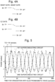
- Fig. 5 shows the result of an experiment in which the energy states of the first and second superconducting circuits 11 and 12 in the quantum gate device 10 shown in Fig. 3 were measured after the electromagnetic wave having a difference frequency
- the first superconducting circuit 11 was irradiated with an electromagnetic wave having the first resonance frequency ⁇ 1 from the first electromagnetic wave irradiator 151, or the second superconducting circuit 12 was irradiated with an electromagnetic wave having the second resonance frequency ⁇ 2 from the second electromagnetic wave irradiator 152, and the irradiation with the electromagnetic wave having a difference frequency
- the circuit is in the ground state (g1 or g2) within the area where the ordinate value is negative, while the circuit is in the first excited state (e1 or e2) within the area where the ordinate value is positive.
- the experimental result shows that, when one of the first and second superconducting circuits 11 and 12 is in the ground state, the other circuit is in the first excited state.
- the energy state of this quantum gate device 10 changes so that it alternates between the two states e1g2 and g1e2 during the irradiation with the electromagnetic wave ( Fig. 4A ).
- T denoting the period of this change in energy state the period of time T/2 required for a change from one state to the other is approximately 16 nanoseconds according to the experimental result shown in Fig. 5 .
- conventional quantum gate devices employing transmons or similar circuits require more than 100 nanoseconds for a change between two states.
- the transition between the two states according to the first embodiment occurs with a shorter period of time (at higher speeds) than in the conventional cases.
- the depiction in Figs. 4A and 4B (which will be described later) assumes that the energy state g1e2 is higher than e1g2, although the energy state e1g2 can be higher than g1e2 depending on the configuration of the first and second superconducting circuits 11 and 12.
- the quantum gate device 10 when the phase of the electromagnetic wave transmitted to the first superconducting circuit 11 and/or the second superconducting circuit 12 is changed by 90 degrees, the ground state and the first excited state are exchanged between the first and second superconducting circuits 11 and 12, and additionally, the phase is inverted in one of the first and second superconducting circuits 11 and 12. That is to say, the device can be operated as an iSWAP gate which changes the state from gle2 to ielg2, or from elg2 to igle2.
- the quantum gate device 10 can also be operated as a CZ gate.
- a CZ gate an electromagnetic wave having a difference frequency
- the quantum gate device 10 can perform three types of operations of the quantum gate, i.e., the SWAP gate, iSWAP gate and CZ gate.
- Fig. 6 is a diagram showing a schematic of the configuration of a quantum gate device 20 according to the second embodiment of the present invention.
- the configuration of this quantum gate device 20 is identical to the quantum gate device 10 according to the first embodiment except that the first electromagnetic wave irradiator (electromagnetic wave irradiator) 151 is replaced by a residual-interaction-cancelling electromagnetic wave irradiator 251 doubling as the first electromagnetic wave irradiator (electromagnetic wave irradiator) which will be described later, and that an irradiation coordinator 21 is added.
- the components except for the residual-interaction-cancelling electromagnetic wave irradiator 251 doubling as the first electromagnetic wave irradiator and the irradiation coordinator 21 are identical in configuration to those of the quantum gate device 10 according to the first embodiment, and therefore, will not be described in detail.
- the residual-interaction-cancelling electromagnetic wave irradiator 251 doubling as the first electromagnetic wave irradiator includes a microwave generator 2511 and a capacitor 2512.
- the microwave generator 2511 generates an electromagnetic wave (microwave) having one of the three frequencies of
- the electromagnetic wave generated by the microwave generator 2511 is transmitted (applied) to the first superconducting circuit 11 through the capacitor 2512.
- the irradiation coordinator 21 is configured to control the timing of the electromagnetic-wave irradiation by the residual-interaction-cancelling electromagnetic wave irradiator 251 doubling as the first electromagnetic wave irradiator.
- the residual-interaction-cancelling electromagnetic wave irradiator 251 doubling as the first electromagnetic wave irradiator produces an electromagnetic wave having a frequency of
- a pulsed electromagnetic wave having a pulse width corresponding to the period of time for inverting the phase of the qubit in the first superconducting circuit 11 ( ⁇ pulse or 180-degree pulse) can be used.
- Fig. 7 shows operations which occur at each point in time in the first and second superconducting circuits 11 and 12 with the passage of time from left to right.
- the quantum gate device 20 performs an operation for cutting off the residual interaction after the operation of the quantum gate, as will be hereinafter described.
- the operation of the quantum gate in the quantum gate device 20 is identical to the operation in the quantum gate device 10 according to the first embodiment regardless of whether it is operated as a SWAP gate, iSWAP gate or CZ gate. That is to say, the quantum gate device 20 is cooled to a temperature equal to or lower than the superconductive transition temperature by the cooling system, and a static magnetic field is applied from the magnetic field applier 14 to the partial superconducting circuit 113. Subsequently, an electromagnetic wave having a predetermined difference frequency is transmitted from the residual-interaction-cancelling electromagnetic wave irradiator 251 doubling as the first electromagnetic wave irradiator to the first superconducting circuit 11.
- the difference frequency is
- a first residual-interaction-cancelling electromagnetic wave 32 having a frequency of ⁇ 1 is transmitted from the residual-interaction-cancelling electromagnetic wave irradiator 251 doubling as the first electromagnetic wave irradiator to the first superconducting circuit 11, whereby the phase of the qubit in the first superconducting circuit 11 is inverted, and the residual interaction with the second superconducting circuit 12 is broken.
- a second residual-interaction-cancelling electromagnetic wave 33 having a frequency of ⁇ 1 is transmitted to the first superconducting circuit 11, whereby the phase of the qubit in the first superconducting circuit 11 is returned to its original state.
- an electromagnetic wave 34 (see Fig. 8 ) which has a frequency of ⁇ 2 and is tuned to change the phase of the qubit in the second superconducting circuit 12 by 90 degrees is transmitted from the second electromagnetic wave irradiator 152 to the second superconducting circuit 12.
- a pulsed electromagnetic wave which is generally called a " ⁇ /2 pulse” or "90-degree pulse” and has conventionally been used for a spin echo method in a magnetic resonance measurement can be used.
- the operation 31 of the quantum gate is performed.
- an electromagnetic wave (e.g., ⁇ /2 pulse) 35 which has a frequency of ⁇ 2 and tuned to change the phase of the qubit in the second superconducting circuit 12 is transmitted from the second electromagnetic wave irradiator 152 to the second superconducting circuit 12.
- a measurement 36 of the output signal of the capacitor 162 is performed. The measurement described thus far is hereinafter called the "first preliminary experiment”. The first preliminary experiment is performed for various values of t and ⁇ .
- a second preliminary experiment is performed.
- an electromagnetic wave (e.g., ⁇ pulse) 37 which inverts the phase of the qubit in the first superconducting circuit 11 is transmitted from the residual-interaction-cancelling electromagnetic wave irradiator 251 doubling as the first electromagnetic wave irradiator to the first superconducting circuit 11 (as indicated by the broken line in Fig. 8 ).
- the operations from the transmission of the electromagnetic wave 34 to the measurement 36 of the output signal of the capacitor 162 are performed in a similar manner to the first preliminary experiment. There is no requirement concerning the length of time between the transmission of the electromagnetic wave 37 and that of the electromagnetic wave 34.
- the second preliminary experiment is performed for various values of t and ⁇ .
- Fig. 9A shows the results of the first and second preliminary experiments performed for various values of t, with ⁇ fixed at a specific value.
- the gate operation was performed for 34 nanoseconds in these preliminary experiments.
- the set of data with the annotation "without irradiation with electromagnetic wave 37" in Fig. 9A are data obtained through the first preliminary experiment, while the set of data with the annotation "with irradiation with electromagnetic wave 37" are data obtained through the second preliminary experiment.
- the output value shows a sinusoidal change with the changing value of t.
- a phase difference ⁇ R occurs between the two sets of data.
- a function expressing ⁇ R with ⁇ as the variable can be obtained, as shown in Fig. 9B.
- Fig. 9B shows two negatively sloped solid lines, of which the left one is the function of ⁇ R in the case where the operation of a SWAP gate was performed, while the right one corresponds to the function of ⁇ R in the case where the operation of a CZ gate was performed.
- the negatively sloped broken line in Fig. 9B is the function of ⁇ R with no operation of the quantum gate.
- ⁇ R with the SWAP-gate operation and those with no quantum-gate operation are indicated on the left-side vertical axis, while the values of ⁇ R with the CZ-gate operation are indicated on the right-side vertical axis.
- a random benchmark test for the quantum gate device 20 according to the second embodiment was performed, which demonstrated that the operation of the quantum gate was correctly performed with a probability of 97.3 ⁇ 0.1 % for the SWAP gate, 97.2 ⁇ 0.1 % for the iSWAP gate and 96.4 ⁇ 0.1 % for the CZ gate. These values are lower (the error occurrence rates are higher) than in the first embodiment, which is most likely due to the fact that a certain amount of time is required for the operation of transmitting the residual-interaction-cancelling electromagnetic wave two times after the operation of the quantum gate.
- Fig. 10 shows an example of the integrated quantum circuit in which a plurality of quantum gate devices 10 according to the first embodiment are integrated.
- This integrated quantum circuit 50 consists of a plurality of quantum gate devices 10 connected in a two-dimensional form (matrix form), in which each pair of quantum gate devices 10 neighboring each other are connected via a capacitor 51.
- the quantum gate devices 10 according to the first embodiment are used in the present example, a plurality of quantum gate devices 20 according to the second embodiment can also be integrated to construct an integrated quantum circuit.
- the present invention is not limited to the previously described embodiments.
- the second superconducting circuit 12 which is a transmon is used in the quantum gate devices 10 and 20 according to the first and second embodiments
- the second superconducting circuit 12 may be replaced by any of the second superconducting circuits 12A, 12B and 12C shown in Figs. 11A-11C .
- the second superconducting circuit 12A shown in Fig. 11A is a so-called charge qubit, in which a Josephson device 121A and a capacitor 124A are connected in series by a second line 125A made of a superconductor.
- FIG. 11B is a so-called flux qubit, in which a plurality of (in the example of Fig. 11B , three) Josephson devices 121B are connected in series, with each Josephson device 121B having a capacitor 124B connected in parallel.
- the components of the second superconducting circuit 12B are connected by a second line 125B made of a superconductor.
- the second superconducting circuit 12C shown in Fig. 11C is a so-called fluxonium, in which a Josephson device 121C, capacitor 124C and coil 126C are connected in parallel by a second line 125C made of a superconductor.
- a first electromagnetic wave irradiator e.g., the same one as the first electromagnetic wave irradiator 151 used in the quantum gate device 10 according to the first embodiment
- a residual-interaction-cancelling electromagnetic wave irradiator may be separately provided.
- the electromagnetic wave irradiator (the first electromagnetic wave irradiator 151) and/or the residual-interaction-cancelling electromagnetic wave irradiator (the residual-interaction-cancelling electromagnetic wave irradiator 251 doubling as the first electromagnetic wave irradiator, or a residual-interaction-cancelling electromagnetic wave irradiator that does not double as the first electromagnetic wave irradiator) may be configured to irradiate only the first superconducting circuit with the electromagnetic wave, or to irradiate the second superconducting circuit with the electromagnetic wave in addition to the first superconducting circuit.
- a plurality of quantum gate devices in which the configurations according to those embodiments and modified examples are combined may be integrated to construct an integrated quantum circuit.
Landscapes
- Engineering & Computer Science (AREA)
- General Physics & Mathematics (AREA)
- Theoretical Computer Science (AREA)
- Physics & Mathematics (AREA)
- Mathematical Analysis (AREA)
- Computing Systems (AREA)
- Evolutionary Computation (AREA)
- Condensed Matter Physics & Semiconductors (AREA)
- Computational Mathematics (AREA)
- Mathematical Optimization (AREA)
- Pure & Applied Mathematics (AREA)
- Data Mining & Analysis (AREA)
- General Engineering & Computer Science (AREA)
- Mathematical Physics (AREA)
- Software Systems (AREA)
- Artificial Intelligence (AREA)
- Superconductor Devices And Manufacturing Methods Thereof (AREA)
- Logic Circuits (AREA)
- Junction Field-Effect Transistors (AREA)
Applications Claiming Priority (2)
| Application Number | Priority Date | Filing Date | Title |
|---|---|---|---|
| JP2019148136 | 2019-08-09 | ||
| PCT/JP2020/008489 WO2021029095A1 (ja) | 2019-08-09 | 2020-02-28 | 量子ゲート装置 |
Publications (3)
| Publication Number | Publication Date |
|---|---|
| EP4012789A1 EP4012789A1 (en) | 2022-06-15 |
| EP4012789A4 EP4012789A4 (en) | 2023-01-04 |
| EP4012789B1 true EP4012789B1 (en) | 2024-02-21 |
Family
ID=74570274
Family Applications (1)
| Application Number | Title | Priority Date | Filing Date |
|---|---|---|---|
| EP20852813.3A Active EP4012789B1 (en) | 2019-08-09 | 2020-02-28 | Quantum gate device |
Country Status (6)
| Country | Link |
|---|---|
| US (1) | US12099902B2 (https=) |
| EP (1) | EP4012789B1 (https=) |
| JP (1) | JP7340878B2 (https=) |
| CN (1) | CN114788025B (https=) |
| TW (1) | TWI803737B (https=) |
| WO (1) | WO2021029095A1 (https=) |
Families Citing this family (4)
| Publication number | Priority date | Publication date | Assignee | Title |
|---|---|---|---|---|
| JP2024526085A (ja) | 2021-06-11 | 2024-07-17 | シーク, インコーポレイテッド | 超伝導量子回路のための磁束バイアスのシステム及び方法 |
| WO2023102654A1 (en) | 2021-12-09 | 2023-06-15 | Anyon Systems Inc. | Methods and circuits for performing two-qubit quantum gates |
| TWI802206B (zh) * | 2022-01-04 | 2023-05-11 | 國立成功大學 | 多貝西d6小波轉換/反轉換量子電路及其製造方法 |
| US20240178844A1 (en) * | 2022-09-28 | 2024-05-30 | Taiwan Semiconductor Manufacturing Company, Ltd. | Quantum computation device and operation thereof |
Family Cites Families (18)
| Publication number | Priority date | Publication date | Assignee | Title |
|---|---|---|---|---|
| US6900454B2 (en) * | 2002-04-20 | 2005-05-31 | D-Wave Systems, Inc. | Resonant controlled qubit system |
| FR2839389B1 (fr) * | 2002-05-03 | 2005-08-05 | Commissariat Energie Atomique | Dispositif de bit quantique supraconducteur a jonctions josephson |
| US7230266B2 (en) * | 2003-05-15 | 2007-06-12 | D-Wave Systems Inc. | Conditional Rabi oscillation readout for quantum computing |
| JP4777718B2 (ja) * | 2005-08-11 | 2011-09-21 | 日本電信電話株式会社 | 量子ビット装置及び量子ビットの制御方法 |
| US8654578B2 (en) * | 2011-06-17 | 2014-02-18 | Northrop Grumman Systems Corporation | Phase qubit cell having enhanced coherence |
| EP3262762B1 (en) * | 2015-02-27 | 2021-11-10 | Yale University | Josephson junction-based circulators and related systems and methods |
| EP3262572B1 (en) * | 2015-02-27 | 2024-04-03 | Yale University | Techniques of oscillator control for quantum information processing and related systems and methods |
| US10097143B2 (en) * | 2015-06-29 | 2018-10-09 | International Business Machines Corporation | Josephson-coupled resonator amplifier (JRA) |
| CA3162818C (en) * | 2015-09-30 | 2025-11-18 | Google Llc | COPLANAR WAVEGUIDE FLUID QUBITS |
| CN114781643B (zh) * | 2015-12-16 | 2023-04-14 | 谷歌有限责任公司 | 利用共面波导通量量子比特的可编程通用量子退火 |
| US10467544B2 (en) | 2015-12-31 | 2019-11-05 | International Business Machines Corporation | Multi-qubit tunable coupling architecture using fixed-frequency superconducting qubits |
| US10042805B2 (en) | 2016-01-21 | 2018-08-07 | Northrop Grumman Systems Corporation | Tunable bus-mediated coupling between remote qubits |
| US10050630B2 (en) * | 2016-08-19 | 2018-08-14 | Rigetti & Co, Inc. | Flux-tunable qubit device with multiple Josephson junctions |
| WO2018063205A1 (en) * | 2016-09-29 | 2018-04-05 | Intel Corporation | On-chip wireless communication devices for qubits |
| US10176432B2 (en) | 2017-03-07 | 2019-01-08 | International Business Machines Corporation | Weakly tunable qubit based on two coupled disparate transmons |
| JP6853141B2 (ja) * | 2017-08-15 | 2021-03-31 | 日本電信電話株式会社 | 超伝導磁束量子ビット制御装置 |
| US10235635B1 (en) * | 2017-10-19 | 2019-03-19 | International Business Machines Corporation | Capacitively-shunted asymmetric DC-SQUID for qubit readout and reset |
| EP3912200B1 (en) * | 2019-01-17 | 2024-05-15 | Yale University | Josephson nonlinear circuit |
-
2020
- 2020-02-28 CN CN202080054500.7A patent/CN114788025B/zh active Active
- 2020-02-28 WO PCT/JP2020/008489 patent/WO2021029095A1/ja not_active Ceased
- 2020-02-28 JP JP2021539811A patent/JP7340878B2/ja active Active
- 2020-02-28 EP EP20852813.3A patent/EP4012789B1/en active Active
- 2020-02-28 US US17/629,718 patent/US12099902B2/en active Active
- 2020-03-04 TW TW109106988A patent/TWI803737B/zh active
Also Published As
| Publication number | Publication date |
|---|---|
| US12099902B2 (en) | 2024-09-24 |
| JPWO2021029095A1 (https=) | 2021-02-18 |
| TWI803737B (zh) | 2023-06-01 |
| WO2021029095A1 (ja) | 2021-02-18 |
| JP7340878B2 (ja) | 2023-09-08 |
| EP4012789A4 (en) | 2023-01-04 |
| CN114788025B (zh) | 2025-07-08 |
| CN114788025A (zh) | 2022-07-22 |
| TW202107744A (zh) | 2021-02-16 |
| EP4012789A1 (en) | 2022-06-15 |
| US20220269968A1 (en) | 2022-08-25 |
Similar Documents
| Publication | Publication Date | Title |
|---|---|---|
| EP4012789B1 (en) | Quantum gate device | |
| Jurcevic et al. | Demonstration of quantum volume 64 on a superconducting quantum computing system | |
| Yurtalan et al. | Implementation of a Walsh-Hadamard gate in a superconducting qutrit | |
| KR102632759B1 (ko) | 초전도 회로를 이용하는 하드웨어 효율적인 장애 허용 연산 | |
| Xiong et al. | Arbitrary controlled-phase gate on fluxonium qubits using differential ac Stark shifts | |
| EP4064137A1 (en) | Quantum circuit and quantum processor | |
| US10467544B2 (en) | Multi-qubit tunable coupling architecture using fixed-frequency superconducting qubits | |
| US11184006B2 (en) | Techniques for manipulation of two-qubit quantum states and related systems and methods | |
| Bianchetti et al. | Control and tomography of a three level superconducting artificial atom | |
| Dehollain et al. | Optimization of a solid-state electron spin qubit using gate set tomography | |
| US11170317B2 (en) | Procedure for systematic tune up of crosstalk in a cross-resonance gate and system performing the procedure and using results of the same | |
| US20150358022A1 (en) | System and method for controlling superconducting quantum circuits using single flux quantum logic circuits | |
| Wu et al. | Geometric phase gates with adiabatic control in electron spin resonance | |
| Alam et al. | Quantum computing hardware for HEP algorithms and sensing | |
| EP4425389A1 (en) | Apparatus and method for leakage reduction in a quantum computing device | |
| Xu et al. | Observation and modulation of the quantum Mpemba effect on a superconducting quantum processor | |
| Debnath et al. | Self-stimulated pulse echo trains from inhomogeneously broadened spin ensembles | |
| Mohiyaddin et al. | Transport of spin qubits with donor chains under realistic experimental conditions | |
| CN115867924A (zh) | 用于操作具有第一和第二量子比特的电路的方法 | |
| US20240311671A1 (en) | Calibration of iSWAP Gate on a Superconducting Quantum Processing Unit | |
| Zhang et al. | Characterization of tunable coupler without a dedicated readout resonator in superconducting circuits | |
| EP4457709A1 (en) | Enhancing the coherence of superconducting quantum bits | |
| Noguchi et al. | Fast parametric two-qubit gates with suppressed residual interaction using a parity-violated superconducting qubit | |
| Lacroix | Quantum Error Correction with Superconducting Circuits | |
| Singh et al. | Simulating three-flavor neutrino oscillations on a nuclear magnetic resonance quantum processor |
Legal Events
| Date | Code | Title | Description |
|---|---|---|---|
| STAA | Information on the status of an ep patent application or granted ep patent |
Free format text: STATUS: THE INTERNATIONAL PUBLICATION HAS BEEN MADE |
|
| PUAI | Public reference made under article 153(3) epc to a published international application that has entered the european phase |
Free format text: ORIGINAL CODE: 0009012 |
|
| STAA | Information on the status of an ep patent application or granted ep patent |
Free format text: STATUS: REQUEST FOR EXAMINATION WAS MADE |
|
| 17P | Request for examination filed |
Effective date: 20220131 |
|
| AK | Designated contracting states |
Kind code of ref document: A1 Designated state(s): AL AT BE BG CH CY CZ DE DK EE ES FI FR GB GR HR HU IE IS IT LI LT LU LV MC MK MT NL NO PL PT RO RS SE SI SK SM TR |
|
| DAV | Request for validation of the european patent (deleted) | ||
| DAX | Request for extension of the european patent (deleted) | ||
| A4 | Supplementary search report drawn up and despatched |
Effective date: 20221202 |
|
| RIC1 | Information provided on ipc code assigned before grant |
Ipc: H01L 27/18 20060101ALI20221128BHEP Ipc: G06N 10/00 20220101ALI20221128BHEP Ipc: H01L 39/22 20060101AFI20221128BHEP |
|
| REG | Reference to a national code |
Ref country code: DE Ipc: H10N0069000000 Ref country code: DE Ref legal event code: R079 Ref document number: 602020026197 Country of ref document: DE Free format text: PREVIOUS MAIN CLASS: H01L0039220000 Ipc: H10N0069000000 |
|
| REG | Reference to a national code |
Ref country code: DE Ref legal event code: R079 Free format text: PREVIOUS MAIN CLASS: H10N0069000000 Ipc: G06N0010400000 Ref document number: 602020026197 Country of ref document: DE |
|
| RIC1 | Information provided on ipc code assigned before grant |
Ipc: H10N 60/10 20230101ALI20230829BHEP Ipc: G06N 10/00 20220101ALI20230829BHEP Ipc: H10N 69/00 20230101AFI20230829BHEP |
|
| GRAP | Despatch of communication of intention to grant a patent |
Free format text: ORIGINAL CODE: EPIDOSNIGR1 |
|
| STAA | Information on the status of an ep patent application or granted ep patent |
Free format text: STATUS: GRANT OF PATENT IS INTENDED |
|
| RIC1 | Information provided on ipc code assigned before grant |
Ipc: H10N 69/00 20230101ALI20230926BHEP Ipc: G06N 10/40 20220101AFI20230926BHEP |
|
| INTG | Intention to grant announced |
Effective date: 20231017 |
|
| GRAS | Grant fee paid |
Free format text: ORIGINAL CODE: EPIDOSNIGR3 |
|
| GRAA | (expected) grant |
Free format text: ORIGINAL CODE: 0009210 |
|
| STAA | Information on the status of an ep patent application or granted ep patent |
Free format text: STATUS: THE PATENT HAS BEEN GRANTED |
|
| AK | Designated contracting states |
Kind code of ref document: B1 Designated state(s): AL AT BE BG CH CY CZ DE DK EE ES FI FR GB GR HR HU IE IS IT LI LT LU LV MC MK MT NL NO PL PT RO RS SE SI SK SM TR |
|
| REG | Reference to a national code |
Ref country code: GB Ref legal event code: FG4D |
|
| REG | Reference to a national code |
Ref country code: CH Ref legal event code: EP |
|
| REG | Reference to a national code |
Ref country code: IE Ref legal event code: FG4D |
|
| REG | Reference to a national code |
Ref country code: DE Ref legal event code: R096 Ref document number: 602020026197 Country of ref document: DE |
|
| REG | Reference to a national code |
Ref country code: LT Ref legal event code: MG9D |
|
| REG | Reference to a national code |
Ref country code: NL Ref legal event code: MP Effective date: 20240221 |
|
| PG25 | Lapsed in a contracting state [announced via postgrant information from national office to epo] |
Ref country code: IS Free format text: LAPSE BECAUSE OF FAILURE TO SUBMIT A TRANSLATION OF THE DESCRIPTION OR TO PAY THE FEE WITHIN THE PRESCRIBED TIME-LIMIT Effective date: 20240621 |
|
| PG25 | Lapsed in a contracting state [announced via postgrant information from national office to epo] |
Ref country code: LT Free format text: LAPSE BECAUSE OF FAILURE TO SUBMIT A TRANSLATION OF THE DESCRIPTION OR TO PAY THE FEE WITHIN THE PRESCRIBED TIME-LIMIT Effective date: 20240221 |
|
| PG25 | Lapsed in a contracting state [announced via postgrant information from national office to epo] |
Ref country code: GR Free format text: LAPSE BECAUSE OF FAILURE TO SUBMIT A TRANSLATION OF THE DESCRIPTION OR TO PAY THE FEE WITHIN THE PRESCRIBED TIME-LIMIT Effective date: 20240522 |
|
| REG | Reference to a national code |
Ref country code: AT Ref legal event code: MK05 Ref document number: 1659740 Country of ref document: AT Kind code of ref document: T Effective date: 20240221 |
|
| PG25 | Lapsed in a contracting state [announced via postgrant information from national office to epo] |
Ref country code: HR Free format text: LAPSE BECAUSE OF FAILURE TO SUBMIT A TRANSLATION OF THE DESCRIPTION OR TO PAY THE FEE WITHIN THE PRESCRIBED TIME-LIMIT Effective date: 20240221 Ref country code: NL Free format text: LAPSE BECAUSE OF FAILURE TO SUBMIT A TRANSLATION OF THE DESCRIPTION OR TO PAY THE FEE WITHIN THE PRESCRIBED TIME-LIMIT Effective date: 20240221 Ref country code: RS Free format text: LAPSE BECAUSE OF FAILURE TO SUBMIT A TRANSLATION OF THE DESCRIPTION OR TO PAY THE FEE WITHIN THE PRESCRIBED TIME-LIMIT Effective date: 20240521 |
|
| PG25 | Lapsed in a contracting state [announced via postgrant information from national office to epo] |
Ref country code: ES Free format text: LAPSE BECAUSE OF FAILURE TO SUBMIT A TRANSLATION OF THE DESCRIPTION OR TO PAY THE FEE WITHIN THE PRESCRIBED TIME-LIMIT Effective date: 20240221 |
|
| PG25 | Lapsed in a contracting state [announced via postgrant information from national office to epo] |
Ref country code: AT Free format text: LAPSE BECAUSE OF FAILURE TO SUBMIT A TRANSLATION OF THE DESCRIPTION OR TO PAY THE FEE WITHIN THE PRESCRIBED TIME-LIMIT Effective date: 20240221 |
|
| PG25 | Lapsed in a contracting state [announced via postgrant information from national office to epo] |
Ref country code: RS Free format text: LAPSE BECAUSE OF FAILURE TO SUBMIT A TRANSLATION OF THE DESCRIPTION OR TO PAY THE FEE WITHIN THE PRESCRIBED TIME-LIMIT Effective date: 20240521 Ref country code: NO Free format text: LAPSE BECAUSE OF FAILURE TO SUBMIT A TRANSLATION OF THE DESCRIPTION OR TO PAY THE FEE WITHIN THE PRESCRIBED TIME-LIMIT Effective date: 20240521 Ref country code: NL Free format text: LAPSE BECAUSE OF FAILURE TO SUBMIT A TRANSLATION OF THE DESCRIPTION OR TO PAY THE FEE WITHIN THE PRESCRIBED TIME-LIMIT Effective date: 20240221 Ref country code: LT Free format text: LAPSE BECAUSE OF FAILURE TO SUBMIT A TRANSLATION OF THE DESCRIPTION OR TO PAY THE FEE WITHIN THE PRESCRIBED TIME-LIMIT Effective date: 20240221 Ref country code: IS Free format text: LAPSE BECAUSE OF FAILURE TO SUBMIT A TRANSLATION OF THE DESCRIPTION OR TO PAY THE FEE WITHIN THE PRESCRIBED TIME-LIMIT Effective date: 20240621 Ref country code: HR Free format text: LAPSE BECAUSE OF FAILURE TO SUBMIT A TRANSLATION OF THE DESCRIPTION OR TO PAY THE FEE WITHIN THE PRESCRIBED TIME-LIMIT Effective date: 20240221 Ref country code: GR Free format text: LAPSE BECAUSE OF FAILURE TO SUBMIT A TRANSLATION OF THE DESCRIPTION OR TO PAY THE FEE WITHIN THE PRESCRIBED TIME-LIMIT Effective date: 20240522 Ref country code: FI Free format text: LAPSE BECAUSE OF FAILURE TO SUBMIT A TRANSLATION OF THE DESCRIPTION OR TO PAY THE FEE WITHIN THE PRESCRIBED TIME-LIMIT Effective date: 20240221 Ref country code: ES Free format text: LAPSE BECAUSE OF FAILURE TO SUBMIT A TRANSLATION OF THE DESCRIPTION OR TO PAY THE FEE WITHIN THE PRESCRIBED TIME-LIMIT Effective date: 20240221 Ref country code: BG Free format text: LAPSE BECAUSE OF FAILURE TO SUBMIT A TRANSLATION OF THE DESCRIPTION OR TO PAY THE FEE WITHIN THE PRESCRIBED TIME-LIMIT Effective date: 20240221 Ref country code: AT Free format text: LAPSE BECAUSE OF FAILURE TO SUBMIT A TRANSLATION OF THE DESCRIPTION OR TO PAY THE FEE WITHIN THE PRESCRIBED TIME-LIMIT Effective date: 20240221 |
|
| PG25 | Lapsed in a contracting state [announced via postgrant information from national office to epo] |
Ref country code: PL Free format text: LAPSE BECAUSE OF FAILURE TO SUBMIT A TRANSLATION OF THE DESCRIPTION OR TO PAY THE FEE WITHIN THE PRESCRIBED TIME-LIMIT Effective date: 20240221 Ref country code: PT Free format text: LAPSE BECAUSE OF FAILURE TO SUBMIT A TRANSLATION OF THE DESCRIPTION OR TO PAY THE FEE WITHIN THE PRESCRIBED TIME-LIMIT Effective date: 20240621 |
|
| PG25 | Lapsed in a contracting state [announced via postgrant information from national office to epo] |
Ref country code: SE Free format text: LAPSE BECAUSE OF FAILURE TO SUBMIT A TRANSLATION OF THE DESCRIPTION OR TO PAY THE FEE WITHIN THE PRESCRIBED TIME-LIMIT Effective date: 20240221 Ref country code: PT Free format text: LAPSE BECAUSE OF FAILURE TO SUBMIT A TRANSLATION OF THE DESCRIPTION OR TO PAY THE FEE WITHIN THE PRESCRIBED TIME-LIMIT Effective date: 20240621 Ref country code: PL Free format text: LAPSE BECAUSE OF FAILURE TO SUBMIT A TRANSLATION OF THE DESCRIPTION OR TO PAY THE FEE WITHIN THE PRESCRIBED TIME-LIMIT Effective date: 20240221 Ref country code: LV Free format text: LAPSE BECAUSE OF FAILURE TO SUBMIT A TRANSLATION OF THE DESCRIPTION OR TO PAY THE FEE WITHIN THE PRESCRIBED TIME-LIMIT Effective date: 20240221 |
|
| REG | Reference to a national code |
Ref country code: CH Ref legal event code: PL |
|
| PG25 | Lapsed in a contracting state [announced via postgrant information from national office to epo] |
Ref country code: DK Free format text: LAPSE BECAUSE OF FAILURE TO SUBMIT A TRANSLATION OF THE DESCRIPTION OR TO PAY THE FEE WITHIN THE PRESCRIBED TIME-LIMIT Effective date: 20240221 |
|
| PG25 | Lapsed in a contracting state [announced via postgrant information from national office to epo] |
Ref country code: SM Free format text: LAPSE BECAUSE OF FAILURE TO SUBMIT A TRANSLATION OF THE DESCRIPTION OR TO PAY THE FEE WITHIN THE PRESCRIBED TIME-LIMIT Effective date: 20240221 |
|
| PG25 | Lapsed in a contracting state [announced via postgrant information from national office to epo] |
Ref country code: LU Free format text: LAPSE BECAUSE OF NON-PAYMENT OF DUE FEES Effective date: 20240228 |
|
| PG25 | Lapsed in a contracting state [announced via postgrant information from national office to epo] |
Ref country code: CH Free format text: LAPSE BECAUSE OF NON-PAYMENT OF DUE FEES Effective date: 20240229 |
|
| PG25 | Lapsed in a contracting state [announced via postgrant information from national office to epo] |
Ref country code: CZ Free format text: LAPSE BECAUSE OF FAILURE TO SUBMIT A TRANSLATION OF THE DESCRIPTION OR TO PAY THE FEE WITHIN THE PRESCRIBED TIME-LIMIT Effective date: 20240221 Ref country code: EE Free format text: LAPSE BECAUSE OF FAILURE TO SUBMIT A TRANSLATION OF THE DESCRIPTION OR TO PAY THE FEE WITHIN THE PRESCRIBED TIME-LIMIT Effective date: 20240221 |
|
| PG25 | Lapsed in a contracting state [announced via postgrant information from national office to epo] |
Ref country code: SK Free format text: LAPSE BECAUSE OF FAILURE TO SUBMIT A TRANSLATION OF THE DESCRIPTION OR TO PAY THE FEE WITHIN THE PRESCRIBED TIME-LIMIT Effective date: 20240221 |
|
| PG25 | Lapsed in a contracting state [announced via postgrant information from national office to epo] |
Ref country code: SM Free format text: LAPSE BECAUSE OF FAILURE TO SUBMIT A TRANSLATION OF THE DESCRIPTION OR TO PAY THE FEE WITHIN THE PRESCRIBED TIME-LIMIT Effective date: 20240221 Ref country code: SK Free format text: LAPSE BECAUSE OF FAILURE TO SUBMIT A TRANSLATION OF THE DESCRIPTION OR TO PAY THE FEE WITHIN THE PRESCRIBED TIME-LIMIT Effective date: 20240221 Ref country code: RO Free format text: LAPSE BECAUSE OF FAILURE TO SUBMIT A TRANSLATION OF THE DESCRIPTION OR TO PAY THE FEE WITHIN THE PRESCRIBED TIME-LIMIT Effective date: 20240221 Ref country code: LU Free format text: LAPSE BECAUSE OF NON-PAYMENT OF DUE FEES Effective date: 20240228 Ref country code: EE Free format text: LAPSE BECAUSE OF FAILURE TO SUBMIT A TRANSLATION OF THE DESCRIPTION OR TO PAY THE FEE WITHIN THE PRESCRIBED TIME-LIMIT Effective date: 20240221 Ref country code: DK Free format text: LAPSE BECAUSE OF FAILURE TO SUBMIT A TRANSLATION OF THE DESCRIPTION OR TO PAY THE FEE WITHIN THE PRESCRIBED TIME-LIMIT Effective date: 20240221 Ref country code: CZ Free format text: LAPSE BECAUSE OF FAILURE TO SUBMIT A TRANSLATION OF THE DESCRIPTION OR TO PAY THE FEE WITHIN THE PRESCRIBED TIME-LIMIT Effective date: 20240221 Ref country code: CH Free format text: LAPSE BECAUSE OF NON-PAYMENT OF DUE FEES Effective date: 20240229 |
|
| PG25 | Lapsed in a contracting state [announced via postgrant information from national office to epo] |
Ref country code: MC Free format text: LAPSE BECAUSE OF FAILURE TO SUBMIT A TRANSLATION OF THE DESCRIPTION OR TO PAY THE FEE WITHIN THE PRESCRIBED TIME-LIMIT Effective date: 20240221 |
|
| REG | Reference to a national code |
Ref country code: DE Ref legal event code: R097 Ref document number: 602020026197 Country of ref document: DE |
|
| PG25 | Lapsed in a contracting state [announced via postgrant information from national office to epo] |
Ref country code: MC Free format text: LAPSE BECAUSE OF FAILURE TO SUBMIT A TRANSLATION OF THE DESCRIPTION OR TO PAY THE FEE WITHIN THE PRESCRIBED TIME-LIMIT Effective date: 20240221 |
|
| PG25 | Lapsed in a contracting state [announced via postgrant information from national office to epo] |
Ref country code: IT Free format text: LAPSE BECAUSE OF FAILURE TO SUBMIT A TRANSLATION OF THE DESCRIPTION OR TO PAY THE FEE WITHIN THE PRESCRIBED TIME-LIMIT Effective date: 20240221 |
|
| REG | Reference to a national code |
Ref country code: BE Ref legal event code: MM Effective date: 20240229 |
|
| PLBE | No opposition filed within time limit |
Free format text: ORIGINAL CODE: 0009261 |
|
| STAA | Information on the status of an ep patent application or granted ep patent |
Free format text: STATUS: NO OPPOSITION FILED WITHIN TIME LIMIT |
|
| PG25 | Lapsed in a contracting state [announced via postgrant information from national office to epo] |
Ref country code: IT Free format text: LAPSE BECAUSE OF FAILURE TO SUBMIT A TRANSLATION OF THE DESCRIPTION OR TO PAY THE FEE WITHIN THE PRESCRIBED TIME-LIMIT Effective date: 20240221 |
|
| PG25 | Lapsed in a contracting state [announced via postgrant information from national office to epo] |
Ref country code: BE Free format text: LAPSE BECAUSE OF NON-PAYMENT OF DUE FEES Effective date: 20240229 |
|
| PG25 | Lapsed in a contracting state [announced via postgrant information from national office to epo] |
Ref country code: IE Free format text: LAPSE BECAUSE OF NON-PAYMENT OF DUE FEES Effective date: 20240228 |
|
| 26N | No opposition filed |
Effective date: 20241122 |
|
| PG25 | Lapsed in a contracting state [announced via postgrant information from national office to epo] |
Ref country code: IE Free format text: LAPSE BECAUSE OF NON-PAYMENT OF DUE FEES Effective date: 20240228 Ref country code: BE Free format text: LAPSE BECAUSE OF NON-PAYMENT OF DUE FEES Effective date: 20240229 |
|
| REG | Reference to a national code |
Ref country code: DE Ref legal event code: R082 Ref document number: 602020026197 Country of ref document: DE Representative=s name: PLASSERAUD IP GMBH, DE |
|
| PG25 | Lapsed in a contracting state [announced via postgrant information from national office to epo] |
Ref country code: SI Free format text: LAPSE BECAUSE OF FAILURE TO SUBMIT A TRANSLATION OF THE DESCRIPTION OR TO PAY THE FEE WITHIN THE PRESCRIBED TIME-LIMIT Effective date: 20240221 |
|
| PG25 | Lapsed in a contracting state [announced via postgrant information from national office to epo] |
Ref country code: CY Free format text: LAPSE BECAUSE OF FAILURE TO SUBMIT A TRANSLATION OF THE DESCRIPTION OR TO PAY THE FEE WITHIN THE PRESCRIBED TIME-LIMIT; INVALID AB INITIO Effective date: 20200228 |
|
| PG25 | Lapsed in a contracting state [announced via postgrant information from national office to epo] |
Ref country code: HU Free format text: LAPSE BECAUSE OF FAILURE TO SUBMIT A TRANSLATION OF THE DESCRIPTION OR TO PAY THE FEE WITHIN THE PRESCRIBED TIME-LIMIT; INVALID AB INITIO Effective date: 20200228 |
|
| PG25 | Lapsed in a contracting state [announced via postgrant information from national office to epo] |
Ref country code: TR Free format text: LAPSE BECAUSE OF FAILURE TO SUBMIT A TRANSLATION OF THE DESCRIPTION OR TO PAY THE FEE WITHIN THE PRESCRIBED TIME-LIMIT Effective date: 20240221 |
|
| PGFP | Annual fee paid to national office [announced via postgrant information from national office to epo] |
Ref country code: GB Payment date: 20260108 Year of fee payment: 7 |
|
| PGFP | Annual fee paid to national office [announced via postgrant information from national office to epo] |
Ref country code: DE Payment date: 20260105 Year of fee payment: 7 |
|
| PGFP | Annual fee paid to national office [announced via postgrant information from national office to epo] |
Ref country code: FR Payment date: 20260108 Year of fee payment: 7 |