EP4002497A1 - Élément électroluminescent, son procédé de fabrication et dispositif d'affichage - Google Patents
Élément électroluminescent, son procédé de fabrication et dispositif d'affichage Download PDFInfo
- Publication number
- EP4002497A1 EP4002497A1 EP20841155.3A EP20841155A EP4002497A1 EP 4002497 A1 EP4002497 A1 EP 4002497A1 EP 20841155 A EP20841155 A EP 20841155A EP 4002497 A1 EP4002497 A1 EP 4002497A1
- Authority
- EP
- European Patent Office
- Prior art keywords
- light
- electrode
- protrusion
- layer
- pattern
- Prior art date
- Legal status (The legal status is an assumption and is not a legal conclusion. Google has not performed a legal analysis and makes no representation as to the accuracy of the status listed.)
- Pending
Links
- 238000000034 method Methods 0.000 title claims abstract description 84
- 238000004519 manufacturing process Methods 0.000 title claims abstract description 43
- 239000004065 semiconductor Substances 0.000 claims abstract description 355
- 238000005530 etching Methods 0.000 claims description 49
- 239000000758 substrate Substances 0.000 claims description 44
- 239000013078 crystal Substances 0.000 claims description 41
- 230000000994 depressogenic effect Effects 0.000 claims description 7
- 239000010410 layer Substances 0.000 description 600
- 239000000463 material Substances 0.000 description 62
- 230000008569 process Effects 0.000 description 40
- 239000011149 active material Substances 0.000 description 26
- 230000000903 blocking effect Effects 0.000 description 18
- 239000011810 insulating material Substances 0.000 description 14
- 239000000203 mixture Substances 0.000 description 13
- 239000011347 resin Substances 0.000 description 12
- 229920005989 resin Polymers 0.000 description 12
- 239000000976 ink Substances 0.000 description 10
- 239000002243 precursor Substances 0.000 description 10
- 229910052751 metal Inorganic materials 0.000 description 9
- 239000002184 metal Substances 0.000 description 9
- VYPSYNLAJGMNEJ-UHFFFAOYSA-N silicon dioxide Inorganic materials O=[Si]=O VYPSYNLAJGMNEJ-UHFFFAOYSA-N 0.000 description 9
- 239000002019 doping agent Substances 0.000 description 8
- 239000007772 electrode material Substances 0.000 description 7
- 238000002161 passivation Methods 0.000 description 7
- 101100231647 Arabidopsis thaliana HOL3 gene Proteins 0.000 description 6
- 102100022052 Cyclin N-terminal domain-containing protein 1 Human genes 0.000 description 6
- 101150028875 HOL1 gene Proteins 0.000 description 6
- 101000900815 Homo sapiens Cyclin N-terminal domain-containing protein 1 Proteins 0.000 description 6
- 239000011229 interlayer Substances 0.000 description 6
- TWNQGVIAIRXVLR-UHFFFAOYSA-N oxo(oxoalumanyloxy)alumane Chemical compound O=[Al]O[Al]=O TWNQGVIAIRXVLR-UHFFFAOYSA-N 0.000 description 6
- 229910052814 silicon oxide Inorganic materials 0.000 description 6
- 239000000126 substance Substances 0.000 description 6
- 229910002704 AlGaN Inorganic materials 0.000 description 5
- 238000001312 dry etching Methods 0.000 description 5
- 229910052738 indium Inorganic materials 0.000 description 5
- APFVFJFRJDLVQX-UHFFFAOYSA-N indium atom Chemical compound [In] APFVFJFRJDLVQX-UHFFFAOYSA-N 0.000 description 5
- 229910052710 silicon Inorganic materials 0.000 description 5
- 101100231646 Arabidopsis thaliana HOL2 gene Proteins 0.000 description 4
- 229910052782 aluminium Inorganic materials 0.000 description 4
- XAGFODPZIPBFFR-UHFFFAOYSA-N aluminium Chemical compound [Al] XAGFODPZIPBFFR-UHFFFAOYSA-N 0.000 description 4
- 239000004020 conductor Substances 0.000 description 4
- 230000000149 penetrating effect Effects 0.000 description 4
- 238000001020 plasma etching Methods 0.000 description 4
- 229910021420 polycrystalline silicon Inorganic materials 0.000 description 4
- 229920000642 polymer Polymers 0.000 description 4
- 238000002310 reflectometry Methods 0.000 description 4
- PXHVJJICTQNCMI-UHFFFAOYSA-N Nickel Chemical compound [Ni] PXHVJJICTQNCMI-UHFFFAOYSA-N 0.000 description 3
- 229910052581 Si3N4 Inorganic materials 0.000 description 3
- XUIMIQQOPSSXEZ-UHFFFAOYSA-N Silicon Chemical compound [Si] XUIMIQQOPSSXEZ-UHFFFAOYSA-N 0.000 description 3
- 230000004888 barrier function Effects 0.000 description 3
- 230000008859 change Effects 0.000 description 3
- 238000005229 chemical vapour deposition Methods 0.000 description 3
- 238000002425 crystallisation Methods 0.000 description 3
- 238000000151 deposition Methods 0.000 description 3
- 230000000694 effects Effects 0.000 description 3
- 230000005684 electric field Effects 0.000 description 3
- 239000012535 impurity Substances 0.000 description 3
- AMGQUBHHOARCQH-UHFFFAOYSA-N indium;oxotin Chemical compound [In].[Sn]=O AMGQUBHHOARCQH-UHFFFAOYSA-N 0.000 description 3
- 229920001721 polyimide Polymers 0.000 description 3
- -1 polyphenylene Polymers 0.000 description 3
- 239000010703 silicon Substances 0.000 description 3
- HQVNEWCFYHHQES-UHFFFAOYSA-N silicon nitride Chemical compound N12[Si]34N5[Si]62N3[Si]51N64 HQVNEWCFYHHQES-UHFFFAOYSA-N 0.000 description 3
- 238000001039 wet etching Methods 0.000 description 3
- YVTHLONGBIQYBO-UHFFFAOYSA-N zinc indium(3+) oxygen(2-) Chemical compound [O--].[Zn++].[In+3] YVTHLONGBIQYBO-UHFFFAOYSA-N 0.000 description 3
- PIGFYZPCRLYGLF-UHFFFAOYSA-N Aluminum nitride Chemical compound [Al]#N PIGFYZPCRLYGLF-UHFFFAOYSA-N 0.000 description 2
- IJGRMHOSHXDMSA-UHFFFAOYSA-N Atomic nitrogen Chemical compound N#N IJGRMHOSHXDMSA-UHFFFAOYSA-N 0.000 description 2
- 239000004322 Butylated hydroxytoluene Substances 0.000 description 2
- NLZUEZXRPGMBCV-UHFFFAOYSA-N Butylhydroxytoluene Chemical compound CC1=CC(C(C)(C)C)=C(O)C(C(C)(C)C)=C1 NLZUEZXRPGMBCV-UHFFFAOYSA-N 0.000 description 2
- 239000004642 Polyimide Substances 0.000 description 2
- BQCADISMDOOEFD-UHFFFAOYSA-N Silver Chemical compound [Ag] BQCADISMDOOEFD-UHFFFAOYSA-N 0.000 description 2
- 229910021417 amorphous silicon Inorganic materials 0.000 description 2
- 238000000231 atomic layer deposition Methods 0.000 description 2
- 229940095259 butylated hydroxytoluene Drugs 0.000 description 2
- 235000010354 butylated hydroxytoluene Nutrition 0.000 description 2
- 239000011651 chromium Substances 0.000 description 2
- 238000007796 conventional method Methods 0.000 description 2
- 239000010949 copper Substances 0.000 description 2
- PMHQVHHXPFUNSP-UHFFFAOYSA-M copper(1+);methylsulfanylmethane;bromide Chemical compound Br[Cu].CSC PMHQVHHXPFUNSP-UHFFFAOYSA-M 0.000 description 2
- 230000008025 crystallization Effects 0.000 description 2
- 238000004720 dielectrophoresis Methods 0.000 description 2
- 238000009826 distribution Methods 0.000 description 2
- 238000007667 floating Methods 0.000 description 2
- 239000007789 gas Substances 0.000 description 2
- 239000011521 glass Substances 0.000 description 2
- 239000010931 gold Substances 0.000 description 2
- 229910010272 inorganic material Inorganic materials 0.000 description 2
- 239000011147 inorganic material Substances 0.000 description 2
- 229910021421 monocrystalline silicon Inorganic materials 0.000 description 2
- 239000000178 monomer Substances 0.000 description 2
- 238000001127 nanoimprint lithography Methods 0.000 description 2
- 239000012071 phase Substances 0.000 description 2
- 238000005240 physical vapour deposition Methods 0.000 description 2
- 229920000515 polycarbonate Polymers 0.000 description 2
- 239000004417 polycarbonate Substances 0.000 description 2
- 238000004151 rapid thermal annealing Methods 0.000 description 2
- 229910052594 sapphire Inorganic materials 0.000 description 2
- 239000010980 sapphire Substances 0.000 description 2
- 229910052709 silver Inorganic materials 0.000 description 2
- 239000004332 silver Substances 0.000 description 2
- 239000002356 single layer Substances 0.000 description 2
- 238000005507 spraying Methods 0.000 description 2
- 229920003002 synthetic resin Polymers 0.000 description 2
- 239000010936 titanium Substances 0.000 description 2
- 229910052725 zinc Inorganic materials 0.000 description 2
- 239000011701 zinc Substances 0.000 description 2
- TYHJXGDMRRJCRY-UHFFFAOYSA-N zinc indium(3+) oxygen(2-) tin(4+) Chemical compound [O-2].[Zn+2].[Sn+4].[In+3] TYHJXGDMRRJCRY-UHFFFAOYSA-N 0.000 description 2
- QNODIIQQMGDSEF-UHFFFAOYSA-N (1-hydroxycyclohexyl)-phenylmethanone Chemical compound C=1C=CC=CC=1C(=O)C1(O)CCCCC1 QNODIIQQMGDSEF-UHFFFAOYSA-N 0.000 description 1
- 239000012956 1-hydroxycyclohexylphenyl-ketone Substances 0.000 description 1
- KXGFMDJXCMQABM-UHFFFAOYSA-N 2-methoxy-6-methylphenol Chemical compound [CH]OC1=CC=CC([CH])=C1O KXGFMDJXCMQABM-UHFFFAOYSA-N 0.000 description 1
- NIXOWILDQLNWCW-UHFFFAOYSA-M Acrylate Chemical compound [O-]C(=O)C=C NIXOWILDQLNWCW-UHFFFAOYSA-M 0.000 description 1
- 229920000178 Acrylic resin Polymers 0.000 description 1
- 239000004925 Acrylic resin Substances 0.000 description 1
- 101100309451 Arabidopsis thaliana SAD2 gene Proteins 0.000 description 1
- VYZAMTAEIAYCRO-UHFFFAOYSA-N Chromium Chemical compound [Cr] VYZAMTAEIAYCRO-UHFFFAOYSA-N 0.000 description 1
- RYGMFSIKBFXOCR-UHFFFAOYSA-N Copper Chemical compound [Cu] RYGMFSIKBFXOCR-UHFFFAOYSA-N 0.000 description 1
- GYHNNYVSQQEPJS-UHFFFAOYSA-N Gallium Chemical compound [Ga] GYHNNYVSQQEPJS-UHFFFAOYSA-N 0.000 description 1
- 229910001218 Gallium arsenide Inorganic materials 0.000 description 1
- 229910019142 PO4 Inorganic materials 0.000 description 1
- 229920000265 Polyparaphenylene Polymers 0.000 description 1
- 239000004734 Polyphenylene sulfide Substances 0.000 description 1
- 239000004793 Polystyrene Substances 0.000 description 1
- RTAQQCXQSZGOHL-UHFFFAOYSA-N Titanium Chemical compound [Ti] RTAQQCXQSZGOHL-UHFFFAOYSA-N 0.000 description 1
- MPIAGWXWVAHQBB-UHFFFAOYSA-N [3-prop-2-enoyloxy-2-[[3-prop-2-enoyloxy-2,2-bis(prop-2-enoyloxymethyl)propoxy]methyl]-2-(prop-2-enoyloxymethyl)propyl] prop-2-enoate Chemical compound C=CC(=O)OCC(COC(=O)C=C)(COC(=O)C=C)COCC(COC(=O)C=C)(COC(=O)C=C)COC(=O)C=C MPIAGWXWVAHQBB-UHFFFAOYSA-N 0.000 description 1
- 125000000217 alkyl group Chemical group 0.000 description 1
- 229910045601 alloy Inorganic materials 0.000 description 1
- 239000000956 alloy Substances 0.000 description 1
- UMIVXZPTRXBADB-UHFFFAOYSA-N benzocyclobutene Chemical compound C1=CC=C2CCC2=C1 UMIVXZPTRXBADB-UHFFFAOYSA-N 0.000 description 1
- 230000005540 biological transmission Effects 0.000 description 1
- MQDJYUACMFCOFT-UHFFFAOYSA-N bis[2-(1-hydroxycyclohexyl)phenyl]methanone Chemical compound C=1C=CC=C(C(=O)C=2C(=CC=CC=2)C2(O)CCCCC2)C=1C1(O)CCCCC1 MQDJYUACMFCOFT-UHFFFAOYSA-N 0.000 description 1
- 229910052804 chromium Inorganic materials 0.000 description 1
- 239000011248 coating agent Substances 0.000 description 1
- 238000000576 coating method Methods 0.000 description 1
- 239000003086 colorant Substances 0.000 description 1
- 150000001875 compounds Chemical class 0.000 description 1
- 229910052802 copper Inorganic materials 0.000 description 1
- 238000005520 cutting process Methods 0.000 description 1
- 230000008021 deposition Effects 0.000 description 1
- 238000011161 development Methods 0.000 description 1
- 238000009792 diffusion process Methods 0.000 description 1
- AJNVQOSZGJRYEI-UHFFFAOYSA-N digallium;oxygen(2-) Chemical compound [O-2].[O-2].[O-2].[Ga+3].[Ga+3] AJNVQOSZGJRYEI-UHFFFAOYSA-N 0.000 description 1
- KPUWHANPEXNPJT-UHFFFAOYSA-N disiloxane Chemical class [SiH3]O[SiH3] KPUWHANPEXNPJT-UHFFFAOYSA-N 0.000 description 1
- 238000000609 electron-beam lithography Methods 0.000 description 1
- 238000000313 electron-beam-induced deposition Methods 0.000 description 1
- 239000003822 epoxy resin Substances 0.000 description 1
- 125000001495 ethyl group Chemical group [H]C([H])([H])C([H])([H])* 0.000 description 1
- 229910052733 gallium Inorganic materials 0.000 description 1
- 229910001195 gallium oxide Inorganic materials 0.000 description 1
- YZZNJYQZJKSEER-UHFFFAOYSA-N gallium tin Chemical compound [Ga].[Sn] YZZNJYQZJKSEER-UHFFFAOYSA-N 0.000 description 1
- PCHJSUWPFVWCPO-UHFFFAOYSA-N gold Chemical compound [Au] PCHJSUWPFVWCPO-UHFFFAOYSA-N 0.000 description 1
- 229910052737 gold Inorganic materials 0.000 description 1
- BHEPBYXIRTUNPN-UHFFFAOYSA-N hydridophosphorus(.) (triplet) Chemical compound [PH] BHEPBYXIRTUNPN-UHFFFAOYSA-N 0.000 description 1
- 230000002209 hydrophobic effect Effects 0.000 description 1
- HRHKULZDDYWVBE-UHFFFAOYSA-N indium;oxozinc;tin Chemical compound [In].[Sn].[Zn]=O HRHKULZDDYWVBE-UHFFFAOYSA-N 0.000 description 1
- 238000009616 inductively coupled plasma Methods 0.000 description 1
- 238000007641 inkjet printing Methods 0.000 description 1
- 150000002500 ions Chemical class 0.000 description 1
- 229910052746 lanthanum Inorganic materials 0.000 description 1
- FZLIPJUXYLNCLC-UHFFFAOYSA-N lanthanum atom Chemical compound [La] FZLIPJUXYLNCLC-UHFFFAOYSA-N 0.000 description 1
- 238000005224 laser annealing Methods 0.000 description 1
- 239000004973 liquid crystal related substance Substances 0.000 description 1
- 239000011159 matrix material Substances 0.000 description 1
- 239000007769 metal material Substances 0.000 description 1
- 125000002496 methyl group Chemical group [H]C([H])([H])* 0.000 description 1
- 238000010295 mobile communication Methods 0.000 description 1
- 238000012986 modification Methods 0.000 description 1
- 230000004048 modification Effects 0.000 description 1
- 229910052759 nickel Inorganic materials 0.000 description 1
- 150000004767 nitrides Chemical class 0.000 description 1
- 229910052757 nitrogen Inorganic materials 0.000 description 1
- 238000009828 non-uniform distribution Methods 0.000 description 1
- 239000011368 organic material Substances 0.000 description 1
- KYKLWYKWCAYAJY-UHFFFAOYSA-N oxotin;zinc Chemical compound [Zn].[Sn]=O KYKLWYKWCAYAJY-UHFFFAOYSA-N 0.000 description 1
- 230000035515 penetration Effects 0.000 description 1
- 230000002093 peripheral effect Effects 0.000 description 1
- 239000005011 phenolic resin Substances 0.000 description 1
- 229920001568 phenolic resin Polymers 0.000 description 1
- 238000000206 photolithography Methods 0.000 description 1
- FSDNTQSJGHSJBG-UHFFFAOYSA-N piperidine-4-carbonitrile Chemical compound N#CC1CCNCC1 FSDNTQSJGHSJBG-UHFFFAOYSA-N 0.000 description 1
- 229920003229 poly(methyl methacrylate) Polymers 0.000 description 1
- 229920006122 polyamide resin Polymers 0.000 description 1
- 229920000647 polyepoxide Polymers 0.000 description 1
- 229920001223 polyethylene glycol Polymers 0.000 description 1
- 239000009719 polyimide resin Substances 0.000 description 1
- 239000002952 polymeric resin Substances 0.000 description 1
- 239000004926 polymethyl methacrylate Substances 0.000 description 1
- 229920000069 polyphenylene sulfide Polymers 0.000 description 1
- 229920002223 polystyrene Polymers 0.000 description 1
- 238000012545 processing Methods 0.000 description 1
- 239000002096 quantum dot Substances 0.000 description 1
- 239000010453 quartz Substances 0.000 description 1
- 230000009467 reduction Effects 0.000 description 1
- 238000011160 research Methods 0.000 description 1
- 239000000377 silicon dioxide Substances 0.000 description 1
- 239000007790 solid phase Substances 0.000 description 1
- 238000007711 solidification Methods 0.000 description 1
- 230000008023 solidification Effects 0.000 description 1
- 238000004544 sputter deposition Methods 0.000 description 1
- 239000000057 synthetic resin Substances 0.000 description 1
- 239000013077 target material Substances 0.000 description 1
- 238000002207 thermal evaporation Methods 0.000 description 1
- 229910001887 tin oxide Inorganic materials 0.000 description 1
- 229910052719 titanium Inorganic materials 0.000 description 1
- 238000012546 transfer Methods 0.000 description 1
- DQWPFSLDHJDLRL-UHFFFAOYSA-N triethyl phosphate Chemical compound CCOP(=O)(OCC)OCC DQWPFSLDHJDLRL-UHFFFAOYSA-N 0.000 description 1
- JLTRXTDYQLMHGR-UHFFFAOYSA-N trimethylaluminium Chemical compound C[Al](C)C JLTRXTDYQLMHGR-UHFFFAOYSA-N 0.000 description 1
- XCZXGTMEAKBVPV-UHFFFAOYSA-N trimethylgallium Chemical compound C[Ga](C)C XCZXGTMEAKBVPV-UHFFFAOYSA-N 0.000 description 1
- 229920006337 unsaturated polyester resin Polymers 0.000 description 1
- XLOMVQKBTHCTTD-UHFFFAOYSA-N zinc oxide Inorganic materials [Zn]=O XLOMVQKBTHCTTD-UHFFFAOYSA-N 0.000 description 1
- 239000011787 zinc oxide Substances 0.000 description 1
Images


Classifications
-
- H—ELECTRICITY
- H01—ELECTRIC ELEMENTS
- H01L—SEMICONDUCTOR DEVICES NOT COVERED BY CLASS H10
- H01L33/00—Semiconductor devices having potential barriers specially adapted for light emission; Processes or apparatus specially adapted for the manufacture or treatment thereof or of parts thereof; Details thereof
- H01L33/36—Semiconductor devices having potential barriers specially adapted for light emission; Processes or apparatus specially adapted for the manufacture or treatment thereof or of parts thereof; Details thereof characterised by the electrodes
- H01L33/38—Semiconductor devices having potential barriers specially adapted for light emission; Processes or apparatus specially adapted for the manufacture or treatment thereof or of parts thereof; Details thereof characterised by the electrodes with a particular shape
- H01L33/382—Semiconductor devices having potential barriers specially adapted for light emission; Processes or apparatus specially adapted for the manufacture or treatment thereof or of parts thereof; Details thereof characterised by the electrodes with a particular shape the electrode extending partially in or entirely through the semiconductor body
-
- H—ELECTRICITY
- H01—ELECTRIC ELEMENTS
- H01L—SEMICONDUCTOR DEVICES NOT COVERED BY CLASS H10
- H01L21/00—Processes or apparatus adapted for the manufacture or treatment of semiconductor or solid state devices or of parts thereof
- H01L21/02—Manufacture or treatment of semiconductor devices or of parts thereof
- H01L21/04—Manufacture or treatment of semiconductor devices or of parts thereof the devices having potential barriers, e.g. a PN junction, depletion layer or carrier concentration layer
- H01L21/18—Manufacture or treatment of semiconductor devices or of parts thereof the devices having potential barriers, e.g. a PN junction, depletion layer or carrier concentration layer the devices having semiconductor bodies comprising elements of Group IV of the Periodic Table or AIIIBV compounds with or without impurities, e.g. doping materials
- H01L21/28—Manufacture of electrodes on semiconductor bodies using processes or apparatus not provided for in groups H01L21/20 - H01L21/268
-
- H—ELECTRICITY
- H01—ELECTRIC ELEMENTS
- H01L—SEMICONDUCTOR DEVICES NOT COVERED BY CLASS H10
- H01L25/00—Assemblies consisting of a plurality of individual semiconductor or other solid state devices ; Multistep manufacturing processes thereof
- H01L25/03—Assemblies consisting of a plurality of individual semiconductor or other solid state devices ; Multistep manufacturing processes thereof all the devices being of a type provided for in the same subgroup of groups H01L27/00 - H01L33/00, or in a single subclass of H10K, H10N, e.g. assemblies of rectifier diodes
- H01L25/04—Assemblies consisting of a plurality of individual semiconductor or other solid state devices ; Multistep manufacturing processes thereof all the devices being of a type provided for in the same subgroup of groups H01L27/00 - H01L33/00, or in a single subclass of H10K, H10N, e.g. assemblies of rectifier diodes the devices not having separate containers
- H01L25/075—Assemblies consisting of a plurality of individual semiconductor or other solid state devices ; Multistep manufacturing processes thereof all the devices being of a type provided for in the same subgroup of groups H01L27/00 - H01L33/00, or in a single subclass of H10K, H10N, e.g. assemblies of rectifier diodes the devices not having separate containers the devices being of a type provided for in group H01L33/00
- H01L25/0753—Assemblies consisting of a plurality of individual semiconductor or other solid state devices ; Multistep manufacturing processes thereof all the devices being of a type provided for in the same subgroup of groups H01L27/00 - H01L33/00, or in a single subclass of H10K, H10N, e.g. assemblies of rectifier diodes the devices not having separate containers the devices being of a type provided for in group H01L33/00 the devices being arranged next to each other
-
- H—ELECTRICITY
- H01—ELECTRIC ELEMENTS
- H01L—SEMICONDUCTOR DEVICES NOT COVERED BY CLASS H10
- H01L27/00—Devices consisting of a plurality of semiconductor or other solid-state components formed in or on a common substrate
- H01L27/15—Devices consisting of a plurality of semiconductor or other solid-state components formed in or on a common substrate including semiconductor components having potential barriers, specially adapted for light emission
- H01L27/153—Devices consisting of a plurality of semiconductor or other solid-state components formed in or on a common substrate including semiconductor components having potential barriers, specially adapted for light emission in a repetitive configuration, e.g. LED bars
- H01L27/156—Devices consisting of a plurality of semiconductor or other solid-state components formed in or on a common substrate including semiconductor components having potential barriers, specially adapted for light emission in a repetitive configuration, e.g. LED bars two-dimensional arrays
-
- H—ELECTRICITY
- H01—ELECTRIC ELEMENTS
- H01L—SEMICONDUCTOR DEVICES NOT COVERED BY CLASS H10
- H01L33/00—Semiconductor devices having potential barriers specially adapted for light emission; Processes or apparatus specially adapted for the manufacture or treatment thereof or of parts thereof; Details thereof
- H01L33/005—Processes
-
- H—ELECTRICITY
- H01—ELECTRIC ELEMENTS
- H01L—SEMICONDUCTOR DEVICES NOT COVERED BY CLASS H10
- H01L33/00—Semiconductor devices having potential barriers specially adapted for light emission; Processes or apparatus specially adapted for the manufacture or treatment thereof or of parts thereof; Details thereof
- H01L33/02—Semiconductor devices having potential barriers specially adapted for light emission; Processes or apparatus specially adapted for the manufacture or treatment thereof or of parts thereof; Details thereof characterised by the semiconductor bodies
- H01L33/20—Semiconductor devices having potential barriers specially adapted for light emission; Processes or apparatus specially adapted for the manufacture or treatment thereof or of parts thereof; Details thereof characterised by the semiconductor bodies with a particular shape, e.g. curved or truncated substrate
- H01L33/22—Roughened surfaces, e.g. at the interface between epitaxial layers
-
- H—ELECTRICITY
- H01—ELECTRIC ELEMENTS
- H01L—SEMICONDUCTOR DEVICES NOT COVERED BY CLASS H10
- H01L25/00—Assemblies consisting of a plurality of individual semiconductor or other solid state devices ; Multistep manufacturing processes thereof
- H01L25/16—Assemblies consisting of a plurality of individual semiconductor or other solid state devices ; Multistep manufacturing processes thereof the devices being of types provided for in two or more different main groups of groups H01L27/00 - H01L33/00, or in a single subclass of H10K, H10N, e.g. forming hybrid circuits
- H01L25/167—Assemblies consisting of a plurality of individual semiconductor or other solid state devices ; Multistep manufacturing processes thereof the devices being of types provided for in two or more different main groups of groups H01L27/00 - H01L33/00, or in a single subclass of H10K, H10N, e.g. forming hybrid circuits comprising optoelectronic devices, e.g. LED, photodiodes
-
- H—ELECTRICITY
- H01—ELECTRIC ELEMENTS
- H01L—SEMICONDUCTOR DEVICES NOT COVERED BY CLASS H10
- H01L2933/00—Details relating to devices covered by the group H01L33/00 but not provided for in its subgroups
- H01L2933/0008—Processes
- H01L2933/0016—Processes relating to electrodes
-
- H—ELECTRICITY
- H01—ELECTRIC ELEMENTS
- H01L—SEMICONDUCTOR DEVICES NOT COVERED BY CLASS H10
- H01L2933/00—Details relating to devices covered by the group H01L33/00 but not provided for in its subgroups
- H01L2933/0008—Processes
- H01L2933/0033—Processes relating to semiconductor body packages
- H01L2933/0066—Processes relating to semiconductor body packages relating to arrangements for conducting electric current to or from the semiconductor body
-
- H—ELECTRICITY
- H01—ELECTRIC ELEMENTS
- H01L—SEMICONDUCTOR DEVICES NOT COVERED BY CLASS H10
- H01L33/00—Semiconductor devices having potential barriers specially adapted for light emission; Processes or apparatus specially adapted for the manufacture or treatment thereof or of parts thereof; Details thereof
- H01L33/005—Processes
- H01L33/0095—Post-treatment of devices, e.g. annealing, recrystallisation or short-circuit elimination
-
- H—ELECTRICITY
- H01—ELECTRIC ELEMENTS
- H01L—SEMICONDUCTOR DEVICES NOT COVERED BY CLASS H10
- H01L33/00—Semiconductor devices having potential barriers specially adapted for light emission; Processes or apparatus specially adapted for the manufacture or treatment thereof or of parts thereof; Details thereof
- H01L33/44—Semiconductor devices having potential barriers specially adapted for light emission; Processes or apparatus specially adapted for the manufacture or treatment thereof or of parts thereof; Details thereof characterised by the coatings, e.g. passivation layer or anti-reflective coating
-
- H—ELECTRICITY
- H01—ELECTRIC ELEMENTS
- H01L—SEMICONDUCTOR DEVICES NOT COVERED BY CLASS H10
- H01L33/00—Semiconductor devices having potential barriers specially adapted for light emission; Processes or apparatus specially adapted for the manufacture or treatment thereof or of parts thereof; Details thereof
- H01L33/48—Semiconductor devices having potential barriers specially adapted for light emission; Processes or apparatus specially adapted for the manufacture or treatment thereof or of parts thereof; Details thereof characterised by the semiconductor body packages
- H01L33/62—Arrangements for conducting electric current to or from the semiconductor body, e.g. lead-frames, wire-bonds or solder balls
Definitions
- the disclosure relates to a light-emitting element, a method for manufacturing same, and a display device.
- OLED organic light-emitting display
- LCD liquid crystal display
- a display panel such as an OLED panel or an LCD panel is a device included in a display device to display an image.
- a light-emitting element may be provided as a light-emitting display panel, and examples of a light-emitting diode (LED) include an organic LED (OLED) using an organic material as a fluorescent material and an inorganic LED using an inorganic material as a fluorescent material.
- OLED organic LED
- LED inorganic LED
- An inorganic LED using an inorganic semiconductor as a fluorescent material has durability even in a high-temperature environment and has higher efficiency in blue light compared to the organic LED.
- a transfer method using a dielectrophoresis (DEP) method has been developed. Accordingly, research is being continuously conducted on the inorganic light-emitting diode having higher durability and efficiency than those of the organic light-emitting diode.
- aspects of the disclosure provide a light-emitting element in which both end surfaces have different roughness and a pattern is formed on an end surface, and a method for manufacturing the light-emitting element.
- aspects of the disclosure provide a display device which includes a plurality of light-emitting elements, each having a different pattern formed on an end surface.
- a light-emitting element comprising: a first semiconductor layer and a second semiconductor layer, an active layer which is disposed between the first semiconductor layer and the second semiconductor layer, and an electrode layer which is disposed on the second semiconductor layer and comprises a first surface and a second surface facing the first surface and contacting the second semiconductor layer, wherein at least any one of the first surface and the second surface of the electrode layer comprises a protrusion pattern protruding from a part thereof.
- the protrusion pattern may comprise a first protrusion, a second protrusion spaced apart from the first protrusion, and a depression between the first protrusion and the second protrusion.
- the second protrusion may surround the first protrusion.
- the protrusion pattern may further comprise a third protrusion spaced apart from the first protrusion and the second protrusion.
- the third protrusion may be formed to surround an outer surface of the second protrusion, and the depression may be formed between the second protrusion and the third protrusion.
- the first protrusion may comprise an area having the same width as that of the second protrusion.
- the first protrusion may comprise an area having a width equal to a distance between the first protrusion and the second protrusion.
- the protrusion pattern may comprise a first protrusion pattern formed on the first surface, and the light-emitting element may extend in a direction and comprise a first end surface on which the first protrusion pattern is formed and a second end surface on which a surface of the first semiconductor layer is formed.
- the first end surface and the second end surface may have different roughness.
- the light-emitting element may further comprise an insulating film which at least partially surrounds side surfaces of the first semiconductor layer and the second semiconductor layer as well as side surfaces of at least the active layer.
- the electrode layer may comprise a second protrusion pattern which is formed on the second surface to contact the second semiconductor layer, and at least a part of a surface of the second semiconductor layer which contacts the second surface of the electrode layer may be depressed to contact protrusions of the second protrusion pattern.
- the protrusion pattern may be also formed on the first surface.
- a method for manufacturing light-emitting elements comprising: providing a semiconductor structure which is formed on a substrate, and forming a plurality of element rods, each comprising a protrusion pattern protruding from at least a part of an upper surface, by etching the semiconductor structure, wherein different protrusion patterns are formed in different areas of the semiconductor structure.
- the forming of the element rods may comprise forming a first pattern layer which comprises first mask patterns spaced apart from each other on the semiconductor structure, forming semiconductor crystals by etching the semiconductor structure along an area between the first mask patterns spaced apart from each other, forming a second pattern layer which comprises second mask patterns spaced apart from each other on the semiconductor crystals, and forming element rods which comprise protrusion patterns by partially etching upper surfaces of the semiconductor crystals along an area in which the second mask patterns are spaced apart from each other.
- the forming of the second pattern layer may be performed after an insulating film surrounding an outer circumferential surface of each of the semiconductor crystals is formed.
- the semiconductor structure may comprise a first area and a second area different from the first area, and the element rods may comprise a first element rod formed in the first area and a second element rod formed in the second area.
- the first mask pattern disposed in the first area and the second mask pattern disposed in the second area may have the same shape.
- the first element rod and the second element rod may have the same diameter.
- the second mask pattern disposed in the first area and the second mask pattern disposed in the second area may have different shapes.
- a first protrusion pattern formed on an upper surface of the first element rod may have a shape different from that of a second protrusion pattern formed on an upper surface of the second element rod.
- the forming of the element rods may comprise forming a third mask layer which comprises third mask patterns spaced apart from each other on the semiconductor structure, forming protrusion patterns by partially etching an upper surface of the semiconductor structure along an area in which the third mask patterns are spaced apart from each other, forming a fourth mask layer which comprises fourth mask patterns spaced apart from each other on the semiconductor structure, and forming element rods by etching the semiconductor structure along an area between the fourth mask patterns spaced apart from each other.
- the first area and the second area may have different light emission amounts.
- a display device comprising: a first electrode and a second electrode spaced apart from the first electrode, and one or more light-emitting elements which are disposed between the first electrode and the second electrode and each comprise a pattern part formed on an end surface, wherein each of the light-emitting elements comprises a first semiconductor layer and a second semiconductor layer, an active layer which is disposed between the first semiconductor layer and the second semiconductor layer, and an electrode layer which is disposed on the second semiconductor layer and comprises a protrusion pattern protruding from at least a part of a surface.
- the protrusion pattern may comprise a first protrusion, a second protrusion spaced apart from the first protrusion, and a depression between the first protrusion and the second protrusion.
- the second protrusion may surround the first protrusion.
- the light-emitting elements may comprise a first light-emitting element comprising a first protrusion pattern and a second light-emitting element comprising a second protrusion pattern different from the first protrusion pattern.
- the number of protrusions included in the first protrusion pattern may be different from the number of protrusions included in the second protrusion pattern.
- a width of each protrusion included in the first protrusion pattern may be different from a width of each protrusion included in the second protrusion pattern.
- First ends of the light-emitting elements may be electrically connected to the first electrode, and second ends may be electrically connected to the second electrode.
- each light-emitting element may be electrically connected to the first electrode, and the first semiconductor layer may be electrically connected to the second electrode.
- the display device may further comprise a first contact electrode which contacts the first ends of the light-emitting elements and the first electrode, and a second contact electrode which contacts the second ends of the light-emitting elements and the second contact electrode.
- the first contact electrode may contact the electrode layer of each light-emitting element, and the second contact may electrode contact the first semiconductor layer.
- light-emitting elements having protrusion patterns may be manufactured through two etching processes for etching a semiconductor structure.
- the light-emitting elements may include different protrusion patterns, and positions at which the light-emitting elements are formed in the semiconductor structure may be identified through the protrusion patterns. Accordingly, when there is a difference between light-emitting characteristics of the manufactured light-emitting elements, the positions at which the light-emitting elements are formed in the semiconductor structure can be identified through the protrusion patterns, and light-emitting characteristics at the positions can be controlled.
- a display device may include light-emitting elements having different protrusion patterns to reduce a difference in light-emitting characteristics and may have uniform light-emitting characteristics in each pixel.
- FIG. 1 is a schematic plan view of a display device according to an embodiment.
- a display device 10 displays moving images or still images.
- the display device 10 may refer to any electronic device that provides a display screen. Examples of the display device 10 may include televisions, notebook computers, monitors, billboards, the Internet of things (IoT), mobile phones, smartphones, tablet personal computers (PCs), electronic watches, smart watches, watch phones, head mounted displays, mobile communication terminals, electronic notebooks, electronic books, portable multimedia players (PMPs), navigation devices, game machines, digital cameras and camcorders, all of which provide a display screen.
- IoT Internet of things
- PCs personal computers
- PMPs portable multimedia players
- navigation devices game machines, digital cameras and camcorders, all of which provide a display screen.
- the display device 10 includes a display panel that provides a display screen.
- Examples of the display panel may include light emitting diode display panels, organic light emitting display panels, quantum dot light emitting display panels, plasma display panels, and field emission display panels.
- a case where a light emitting diode display panel is applied as an example of the display panel will be described below, but the disclosure is not limited to this case, and other display panels can also be applied as long as the same technical spirit is applicable.
- the shape of the display device 10 can be variously modified.
- the display device 10 may have various shapes such as a horizontally long rectangle, a vertically long rectangle, a square, a quadrangle with rounded corners (vertices), other polygons, and a circle.
- the shape of a display area DA of the display device 10 may also be similar to the overall shape of the display device 10. In FIG. 1 , the display device 10 and the display area DA have a horizontally long rectangular shape.
- the display device 10 may include the display area DA and a non-display area NDA.
- the display area DA may be an area where a screen can be displayed, and the non-display area NDA may be an area where no screen is displayed.
- the display area DA may also be referred to as an active area, and the non-display area NDA may also be referred to as an inactive area.
- the display area DA may generally occupy the center of the display device 10.
- the display area DA may include a plurality of pixels PX.
- the pixels PX may be arranged in a matrix direction.
- Each of the pixels PX may be rectangular or square in plan view. However, the disclosure is not limited thereto, and each of the pixels PX may also have a rhombus shape having each side inclined with respect to a direction.
- Each of the pixels PX may display a specific color by including one or more light-emitting elements 300 which emit light of a specific wavelength band.
- FIG. 2 is a schematic plan view of a pixel of the display device according to the embodiment.
- FIG. 3 is a plan view of a subpixel of FIG. 2 .
- each of the pixels PX may include a first subpixel PX1, a second subpixel PX2, and a third subpixel PX3.
- the first subpixel PX1 may emit light of a first color
- the second subpixel PX2 may emit light of a second color
- the third subpixel PX3 may emit light of a third color.
- the first color may be blue
- the second color may be green
- the third color may be red.
- the disclosure is not limited thereto, and the subpixels PXn may also emit light of the same color.
- a pixel PX includes three subpixels PXn in FIG. 2 , the disclosure is not limited thereto, and the pixel PX may also include more subpixels PXn.
- Each subpixel PXn of the display device 10 may include an area defined as an emission area EMA.
- the first subpixel PX1 may include a first emission area EMA1
- the second subpixel PX2 may include a second emission area EMA2
- the third subpixel PX3 may include a third emission area EMA3.
- the emission area EMA may be defined as an area where light-emitting elements 300 included in the display device 10 are disposed to emit light of a specific wavelength band.
- Each of the light-emitting elements 300 may include an active layer 330, and the active layer 330 may emit light of a specific wavelength band without directionality.
- each light-emitting element 300 may be radiated in a lateral direction of the light-emitting element 300 as well as toward both ends of the light-emitting element 300.
- the emission area EMA of each subpixel PXn may include an area in which the light-emitting elements 300 are disposed and an area which is adjacent to the light-emitting elements 300 and from which light emitted from the light-emitting elements 300 is output.
- the disclosure is not limited thereto, and the emission area EMA may also include an area from which light emitted from the light-emitting elements 300 is output after being reflected or refracted by other members.
- a plurality of light-emitting elements 300 may be disposed in each subpixel PXn, and an area where the light-emitting elements 300 are disposed and an area adjacent to this area may form the emission area EMA.
- each subpixel PXn of the display device 10 may include a non-emission area defined as an area other than the emission area EMA.
- the non-emission area may be an area in which the light-emitting elements 300 are not disposed and from which no light is output because light emitted from the light-emitting elements 300 does not reach this area.
- Each subpixel PXn of the display device 10 may include a plurality of electrodes 210 and 220, the light-emitting elements 300, a plurality of contact electrodes 260, a plurality of inner banks 410 and 420 (see FIG. 4 ), an outer bank 430, and one or more insulating layers 510, 520 and 550 (see FIG. 4 ).
- the electrodes 210 and 220 may be electrically connected to the light-emitting elements 300 and may receive a predetermined voltage so that the light-emitting elements 300 can emit light of a specific wavelength band. In addition, at least a part of each of the electrodes 210 and 220 may be utilized to form an electric field in a subpixel PXn to align the light-emitting elements 300.
- the electrodes 210 and 220 may include a first electrode 210 and a second electrode 220.
- the first electrode 210 may be a pixel electrode separate for each subpixel PXn
- the second electrode 220 may be a common electrode commonly connected along each subpixel PXn.
- Any one of the first electrode 210 and the second electrode 220 may be anodes of the light-emitting elements 300, and the other may be cathodes of the light-emitting elements 300.
- the disclosure is not limited thereto, and the opposite may also be true.
- Each of the first electrode 210 and the second electrode 220 may include an electrode stem part 210S or 220S extending in a first direction DR1 and at least one electrode branch part 210B or 220B extending and branching from the electrode stem part 210S or 220S in a second direction DR2 intersecting the first direction DR1.
- the first electrode 210 may include a first electrode stem part 210S extending in the first direction DR1 and at least one first electrode branch part 210B branching from the first electrode stem part 210S and extending in the second direction DR2.
- the first electrode stem part 210S of any one pixel may have both ends ending between subpixels PXn and spaced apart from ends of neighboring first electrode stem parts 210S but may lie on substantially the same straight line as the first electrode stem parts 210S of neighboring subpixels (e.g., adjacent in the first direction DR1) in the same row. Since both ends of the first electrode stem parts 210S respectively disposed in the subpixels PXn are spaced apart from each other, a different electrical signal may be transmitted to each first electrode branch part 210B, and each first electrode branch part 210B may be driven separately.
- the first electrode branch part 210B may branch from at least a part of the first electrode stem part 210S and extend in the second direction DR2 to end at a position spaced apart from a second electrode stem part 220S facing the first electrode stem part 210S.
- the second electrode 220 may include the second electrode stem part 220S extending in the first direction DR1 and spaced apart from the first electrode stem part 210S in the second direction DR2 to face the first electrode stem part 210S and a second electrode branch part 220B branching from the second electrode stem part 220S and extending in the second direction DR2.
- the other end of the second electrode stem part 220S may be connected to the second electrode stem part 220S of another subpixel PXn adjacent in the first direction DR1. That is, unlike the first electrode stem part 210S, the second electrode stem part 220S may extend in the first direction DR1 to cross the subpixels PXn.
- the second electrode stem part 220S crossing the subpixels PXn may be connected to a peripheral part of the display area DA in which each pixel PX or subpixel PXn is disposed or a part extending in a direction in the non-display area NDA.
- the second electrode branch part 220B may be spaced apart from the first electrode branch part 210B to face the first electrode branch part 210B and may end at a position spaced apart from the first electrode stem part 210S.
- the second electrode branch part 220B may be connected to the second electrode stem part 220S, and an end in the extending direction may be spaced apart from the first electrode stem part 210S in each subpixel PXn.
- the first electrode 210 and the second electrode 220 may be electrically connected to a circuit element layer PAL (see FIG. 4 ) of the display device 10 through contact holes, for example, a first electrode contact hole CNTD and a second electrode contact hole CNTS, respectively.
- the first electrode contact hole CNTD is formed in the first electrode stem part 210S of each subpixel PXn, and only one second electrode contact hole CNTS is formed in one second electrode stem part 220S crossing the subpixels PXn.
- the disclosure is not limited thereto.
- the second electrode contact hole CNTS may also be formed in each subpixel PXn.
- first electrode branch parts 210B are disposed in each subpixel PXn and one second electrode branch part 220B is disposed between them in the drawings, the disclosure is not limited thereto.
- the first electrode 210 and the second electrode 220 may not necessarily extend in one direction and may also be disposed in various structures.
- the first electrode 210 and the second electrode 220 may be partially curved or bent, or any one of the first electrode 210 and the second electrode 220 may surround the other electrode.
- the structure or shape in which the first electrode 210 and the second electrode 220 are disposed is not particularly limited as long as the first electrode 210 and the second electrode 220 are at least partially spaced apart to face each other so that a space in which the light-emitting elements 300 are to be disposed can be formed between the first electrode 210 and the second electrode 220.
- the electrode stem parts 210S and 220S may be omitted from the first electrode 210 and the second electrode 220, respectively.
- the first electrode 210 and the second electrode 220 may only extend in one direction and may be spaced apart from each other in each subpixel PXn. This will be described with reference to another embodiment.
- the banks 410, 420 and 430 may include the outer bank 430 disposed at a boundary between the subpixels PXn and the inner banks 410 and 420 disposed adjacent to the center of each subpixel PXn and under the electrodes 210 and 220, respectively.
- the inner banks 410 and 420 are not illustrated in the drawings, a first inner bank 410 and a second inner bank 420 may be disposed under the first electrode branch part 210B and the second electrode branch part 220B, respectively. These will be described later with reference to other drawings.
- the outer bank 430 may be disposed at the boundary between the subpixels PXn. Respective ends of a plurality of first electrode stem parts 210S may be spaced apart from each other by the outer bank 430.
- the outer bank 430 may extend in the second direction DR2 to lie at the boundary between the subpixels PXn arranged in the first direction DR1. However, the disclosure is not limited thereto, and the outer bank 430 may also extend in the first direction DR1 to lie at the boundary between the subpixels PXn arranged in the second direction DR2.
- the outer bank 430 may include the same material as the inner banks 410 and 420 and may be formed at the same time as the inner banks 410 and 420 in one process.
- the light-emitting elements 300 may be disposed between the first electrode 210 and the second electrode 220. An end of each of the light-emitting elements 300 may be electrically connected to the first electrode 210, and the other end may be electrically connected to the second electrode 220. The light-emitting elements 300 may be electrically connected to the first electrode 210 and the second electrode 220 respectively through the contact electrodes 260 to be described later.
- the light-emitting elements 300 may be spaced apart from each other and may be aligned substantially parallel to each other. A gap between the light-emitting elements 300 is not particularly limited. In some cases, a plurality of light-emitting elements 300 may be disposed adjacent to each other to form a group, and a plurality of other light-emitting elements 300 may form a group at a certain distance from the above group or may be oriented and aligned in a direction with non-uniform density.
- the light-emitting elements 300 may extend in a direction, and the direction in which each electrode, for example, the first electrode branch part 210B and the second electrode branch part 220B extend and the direction in which the light-emitting elements 300 extend may be substantially perpendicular to each other.
- the disclosure is not limited thereto, and the light-emitting elements 300 may also extend in a direction not perpendicular but oblique to the direction in which the first electrode branch part 210B and the second electrode branch part 220B extend.
- the light-emitting elements 300 may include the active layers 330 including different materials to emit light of different wavelength bands to the outside.
- the display device 10 may include the light-emitting elements 300 emitting light of different wavelength bands.
- the light-emitting elements 300 disposed in the subpixels PXn may include the active layers 330 having the same structure but emitting different light.
- the light emitting elements 300 of the first subpixel PX1 may include the active layers 330 emitting first light L1 whose central wavelength band is a first wavelength.
- the light-emitting elements 300 of the second subpixel PX2 may include the active layers 330 emitting second light L2 whose central wavelength band is a second wavelength.
- the light emitting elements 300 of the third subpixel PXn may include the active layers 330 emitting third light L3 whose central wavelength band is a third wavelength.
- the first light L1 may be emitted from the first subpixel PX1
- the second light L2 may be emitted from the second subpixel PX2
- the third light L3 may be emitted from the third subpixel PX3.
- the first light L1 may be blue light whose central wavelength band is in the range of 450 to 495 nm
- the second light L2 may be green light whose central wavelength band is in the range of 495 to 570 nm
- the third light L3 may be red light whose central wavelength band is in the range of 620 to 752 nm.
- the first light L1, the second light L2, and the third light L3 may be light of different colors or light of the same color, and their central wavelength bands may also be different from the above ranges.
- the first subpixel PX1, the second subpixel PX2, and the third subpixel PX3 may include the light-emitting elements 300 of the same type to emit light of substantially the same color.
- the light-emitting elements 300 disposed in each subpixel PXn may include first light-emitting elements 301, second light-emitting elements 302, and third light-emitting elements 303 disposed between the first electrode branch part 210B and the second electrode branch part 220B.
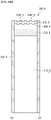
- a process of manufacturing the light-emitting elements 300 may include etching a semiconductor structure 3000 (see FIG. 11 ) formed on a lower substrate 1000 (see FIG. 10 ) in a direction.
- the semiconductor structure 3000 may include an active layer 3300 having a different composition according to position, and there may be a difference in the wavelength band of light emitted from the active layer 3300. In order to minimize a difference between light emitted from the light-emitting elements 300, it may be necessary to control a composition ratio of the active layer 3300 according to position in the semiconductor structure 3000.
- a method for manufacturing the light-emitting elements 300 may include forming a different pattern according to position in the active layer 3300. Accordingly, the manufactured light-emitting elements 300 may include different patterns on their end surfaces, and positions at which the light-emitting elements 300 are formed in the semiconductor structure 3000 can be identified through the patterns. In order to adjust emission characteristics of light emitted from some light-emitting elements 300, composition ratios at specific positions in the semiconductor structure 3000 may be adjusted through the patterns of the light-emitting elements 300.
- the display device 10 according to the embodiment may include the light-emitting elements 300 having different patterns, for example, the first light-emitting elements 301, the second light-emitting elements 302, and the third light-emitting elements 303. The patterns of the light-emitting elements 300 will be described later.
- the display device 10 may include a second insulating layer 510 which at least partially covers the first electrode 210 and the second electrode 220.
- the second insulating layer 510 may be disposed in each subpixel PXn of the display device 10.
- the second insulating layer 510 may substantially entirely cover each subpixel PXn and may also extend to other neighboring subpixels PXn.
- the second insulating layer 510 may at least partially cover the first electrode 210 and the second electrode 220.
- the second insulating layer 510 may be disposed to partially expose the first electrode 210 and the second electrode 220, specifically, partially expose the first electrode branch part 210B and the second electrode branch part 220B.
- each of the contact electrodes 260 may extend in a direction.
- the contact electrodes 260 may contact the light-emitting elements 300 and the electrodes 210 and 220, and the light-emitting elements 300 may receive an electrical signal from the first electrode 210 and the second electrode 220 through the contact electrodes 260.
- the contact electrodes 260 may include a first contact electrode 261 and a second contact electrode 262.
- the first contact electrode 261 and the second contact electrode 262 may be disposed on the first electrode branch part 210B and the second electrode branch part 220B, respectively.
- the first contact electrode 261 may be disposed on the first electrode 210 or the first electrode branch part 210B to extend in the second direction DR2.
- the first contact electrode 261 may contact an end of each of the light-emitting elements 300.
- the first contact electrode 261 may contact the first electrode 210 exposed without the second insulating layer 510 disposed thereon. Accordingly, the light-emitting elements 300 may be electrically connected to the first electrode 210 through the first contact electrode 261.
- the second contact electrode 262 may be disposed on the second electrode 220 or the second electrode branch part 220B to extend in the second direction DR2.
- the second contact electrode 262 may be spaced apart from the first contact electrode 261 in the first direction DR1.
- the second contact electrode 262 may contact the other end of each of the light-emitting elements 300.
- the second contact electrode 262 may contact the second electrode 220 exposed without the second insulating layer 510 disposed thereon. Accordingly, the light-emitting elements 300 may be electrically connected to the second electrode 220 through the second contact electrode 262.
- two first contact electrodes 261 and one second contact electrode 262 are disposed in one subpixel PXn in the drawings, the disclosure is not limited thereto.
- the number of first contact electrodes 261 and second contact electrodes 262 may vary according to the number of first electrodes 210 and second electrodes 220 or the number of first electrode branch parts 210B and second electrode branch parts 220B disposed in each subpixel PXn.
- widths of the first contact electrode 261 and the second contact electrode 262 measured in a direction may respectively be greater than widths of the first electrode 210 and the second electrode 220 or widths of the first electrode branch part 210B and the second electrode branch part 220B measured in the direction.
- Each of the first contact electrode 261 and the second contact electrode 262 may cover sides of the first electrode 210 or the second electrode 220 or sides of the first electrode branch part 210B or the second electrode branch part 220B.
- the disclosure is not limited thereto. In some cases, each of the first contact electrode 261 and the second contact electrode 262 may cover only one side of the first electrode branch part 210B or the second electrode branch part 220B.
- the display device 10 may include the circuit element layer PAL which is located under each of the electrodes 210 and 220 and a third insulating layer 520 (see FIG. 4 ) and a passivation layer 550 (see FIG. 4 ) which at least partially cover each electrode 210 or 220 and the light-emitting elements 300.
- the structure of the display device 10 will now be described in detail with reference to FIG. 4 .
- FIG. 4 is a cross-sectional view taken along lines Xa-Xa', Xb-Xb' and Xc-Xc' of FIG. 3 .
- FIG. 4 illustrates a cross section of only the first subpixel PX1, but the same illustration may be applied to other pixels PX or subpixels PXn.
- FIG. 4 illustrates a cross section across an end and the other end of a light-emitting element 300 disposed in the first subpixel PX1.
- the display device 10 may include the circuit element layer PAL and a light emitting layer EML.
- the circuit element layer PAL may include a substrate 110, a buffer layer 115, light blocking layers BML, first and second transistors 120 and 140, etc.
- the light emitting layer EML may include a plurality of electrodes 210 and 220, the light-emitting elements 300, a plurality of insulating layers 510, 520 and 550, etc. disposed on the first and second transistors 120 and 140.
- the substrate 110 may be an insulating substrate.
- the substrate 110 may be made of an insulating material such as glass, quartz, or polymer resin.
- the substrate 110 may be a rigid substrate, but may also be a flexible substrate that can be bent, folded, rolled, etc.
- the light blocking layers BML may be disposed on the substrate 110.
- the light blocking layers BML may include a first light blocking layer BML1 and a second light blocking layer BML2.
- the first light blocking layer BML1 may be electrically connected to a first drain electrode 123 of the first transistor 120 which will be described later.
- the second light blocking layer BML2 may be electrically connected to a second drain electrode 143 of the second transistor 140.
- the first light blocking layer BML1 and the second light blocking layer BML2 are overlapped by a first active material layer 126 of the first transistor 120 and a second active material layer 146 of the second transistor 140, respectively.
- the first and second light blocking layers BML1 and BML2 may include a light blocking material to prevent light from entering the first and second active material layers 126 and 146.
- the first and second light blocking layers BML1 and BML2 may be made of an opaque metal material that blocks transmission of light.
- the disclosure is not limited thereto. In some cases, the light blocking layers BML may be omitted.
- the buffer layer 115 is disposed on the light blocking layers BML and the substrate 110.
- the buffer layer 115 may entirely cover the substrate 110 as well as the light blocking layers BML.
- the buffer layer 115 may prevent diffusion of impurity ions, prevent penetration of moisture or outside air, and perform a surface planarization function.
- the buffer layer 115 may insulate the light blocking layers BML and the first and second active material layers 126 and 146 from each other.
- a semiconductor layer is disposed on the buffer layer 115.
- the semiconductor layer may include the first active material layer 126 of the first transistor 120, the second active material layer 146 of the second transistor 140, and an auxiliary layer 163.
- the semiconductor layer may include polycrystalline silicon, monocrystalline silicon, an oxide semiconductor, or the like.
- the first active material layer 126 may include a first doped region 126a, a second doped region 126b, and a first channel region 126c.
- the first channel region 126c may be disposed between the first doped region 126a and the second doped region 126b.
- the second active material layer 146 may include a third doped region 146a, a fourth doped region 146b, and a second channel region 146c.
- the second channel region 146c may be disposed between the third doped region 146a and the fourth doped region 146b.
- the first active material layer 126 and the second active material layer 146 may include polycrystalline silicon.
- the polycrystalline silicon may be formed by crystalizing amorphous silicon.
- the crystallization method may include, but are not limited to, a rapid thermal annealing (RTA) method, a solid phase crystallization (SPC) method, an excimer laser annealing (ELA) method, a metal induced crystallization (MILC) method, and a sequential lateral solidification (SLS) method.
- RTA rapid thermal annealing
- SPC solid phase crystallization
- ELA excimer laser annealing
- MILC metal induced crystallization
- SLS sequential lateral solidification
- the first active material layer 126 and the second active material layer 146 may include monocrystalline silicon, low-temperature polycrystalline silicon, amorphous silicon, or the like.
- the first doped region 126a, the second doped region 126b, the third doped region 146a, and the fourth doped region 146b may be, but are not limited to, regions of the first active material layer 126 and the second active material layer 146 which are doped with impurities.
- the first active material layer 126 and the second active material layer 146 are not necessarily limited to the above description.
- the first active material layer 126 and the second active material layer 146 may include an oxide semiconductor.
- the first doped region 126a and the third doped region 146a may be first conducting regions
- the second doped region 126b and the fourth doped region 146b may be second conducting regions.
- the oxide semiconductor may be an oxide semiconductor containing indium (In).
- the oxide semiconductor may be, but is not limited to, indium tin oxide (ITO), indium zinc oxide (IZO), indium gallium oxide (IGO), indium zinc tin oxide (IZTO), indium gallium tin oxide (IGTO), or indium gallium zinc tin oxide (IGZTO).
- ITO indium tin oxide
- IZO indium zinc oxide
- IGO indium gallium oxide
- IZTO indium zinc tin oxide
- IGTO indium gallium tin oxide
- IGZTO indium gallium zinc tin oxide
- a first gate insulating layer 150 is disposed on the semiconductor layer.
- the first gate insulating layer 150 may entirely cover the buffer layer 115 as well as the semiconductor layer.
- the first gate insulating layer 150 may function as a gate insulating layer of each of the first and second transistors 120 and 140.
- a first conductive layer is disposed on the first gate insulating layer 150.
- the first conductive layer disposed on the first gate insulating layer 150 may include a first gate electrode 121 disposed on the first active material layer 126 of the first transistor 120, a second gate electrode 141 disposed on the second active material layer 146 of the second transistor 140, and a power wiring 161 disposed on the auxiliary layer 163.
- the first gate electrode 121 may overlap the first channel region 126c of the first active material layer 126
- the second gate electrode 141 may overlap the second channel region 146c of the second active material layer 146.
- An interlayer insulating film 170 is disposed on the first conductive layer.
- the interlayer insulating film 170 may function as an insulating film between the first conductive layer and other layers disposed on the first conductive layer.
- the interlayer insulating film 170 may include an organic insulating material and perform a surface planarization function.
- a second conductive layer is disposed on the interlayer insulating film 170.
- the second conductive layer includes the first drain electrode 123 and a first source electrode 124 of the first transistor 120, the second drain electrode 143 and a second source electrode 144 of the second transistor 140, and a power electrode 162 disposed on the power wiring 161.
- the first drain electrode 123 and the first source electrode 124 may respectively contact the first doped region 126a and the second doped region 126b of the first active material layer 126 through contact holes penetrating the interlayer insulating film 170 and the first gate insulating layer 150.
- the second drain electrode 143 and the second source electrode 144 may respectively contact the third doped region 146a and the fourth doped region 146b of the second active material layer 146 through contact holes penetrating the interlayer insulating film 170 and the first gate insulating layer 150.
- the first drain electrode 123 and the second drain electrode 143 may be electrically connected to the first light blocking layer BML1 and the second light blocking layer BML2 through other contact holes, respectively.
- a first insulating layer 200 is disposed on the second conductive layer.
- the first insulating layer 200 may include an organic insulating material and perform a surface planarization function.
- the inner banks 410 and 420, the outer bank 430, the electrodes 210 and 220, and the light-emitting elements 300 may be disposed on the first insulating layer 200.
- the banks 410, 420 and 430 may include the inner banks 410 and 420 spaced apart from each other in each subpixel PXn and the outer bank 430 disposed at the boundary between neighboring subpixels PXn.
- the outer bank 430 may extend in the second direction DR2 to lie at the boundary between the subpixels PXn arranged in the first direction DR1. However, the disclosure is not limited thereto, and the outer bank 430 may also extend in the first direction DR1 to lie at the boundary between the subpixels PXn arranged in the second direction DR2. That is, the outer bank 430 may define the boundary of each subpixel PXn.
- the outer bank 430 may prevent the ink from flowing over the boundary of each subpixel PXn.
- the outer bank 430 may separate inks in which different light-emitting elements 300 are dispersed for different subpixels PXn, so that the inks are not mixed with each other.
- the disclosure is not limited thereto.
- the inner banks 410 and 420 may include the first inner bank 410 and the second inner bank 420 disposed adjacent to the center of each subpixel PXn.
- the first inner bank 410 and the second inner bank 420 are spaced apart to face each other.
- the first electrode 210 may be disposed on the first inner bank 410
- the second electrode 220 may be disposed on the second inner bank 420. It may be understood from FIGS. 3 and 4 that the first electrode branch part 210B is disposed on the first inner bank 410 and the second electrode branch part 220B is disposed on the second inner bank 420.
- the first inner bank 410 and the second inner bank 420 may extend in the second direction DR2 in each subpixel PXn. Although not illustrated in the drawings, the first inner bank 410 and the second inner bank 420 may extend in the second direction DR2 toward a subpixel PXn neighboring in the second direction DR2. However, the disclosure is not limited thereto, and the first inner bank 410 and the second inner bank 420 may be disposed in each subpixel PXn to form patterns in the entire display device 10.
- the banks 410, 420 and 430 may include, but are not limited to, polyimide (PI).
- each of the first inner bank 410 and the second inner bank 420 may protrude from the first insulating layer 200.
- Each of the first inner bank 410 and the second inner bank 420 may protrude upward from a plane in which the light-emitting elements 300 are disposed, and the protruding part may be at least partially inclined.
- the protruding shape of each of the first inner bank 410 and the second inner bank 420 is not particularly limited. Since the inner banks 410 and 420 protruding from the first insulating layer 200 have inclined side surfaces, light emitted from the light-emitting elements 300 may be reflected by the inclined side surfaces of the inner banks 410 and 420.
- the electrodes 210 and 220 disposed on the inner banks 410 and 420 include a material having high reflectivity, light emitted from the light-emitting elements 300 may be reflected by the electrodes 210 and 220 located on the inclined side surfaces of the inner banks 410 and 420 to travel upward above the first insulating layer 200.
- the banks 410, 420 and 430 may include the same material and may be formed in the same process.
- the outer bank 430 is disposed at the boundary of each subpixel PXn to form a grid pattern
- the inner banks 410 and 420 are disposed in each subpixel PXn to extend in a direction.
- the outer bank 430 separates neighboring subpixels PXn and prevents ink from overflowing to adjacent subpixels PXn in an inkjet process
- the inner banks 410 and 420 have a protruding structure in each subpixel PXn to function as reflective barriers that reflect light emitted from the light-emitting elements 300 upward above the first insulating layer 200.
- the disclosure is not limited thereto.
- the electrodes 210 and 220 may be disposed on the first insulating layer 200 and the inner banks 410 and 420. As described above, each of the electrodes 210 and 220 includes the electrode stem part 210S or 220S and the electrode branch part 210B or 220B.
- the line Xa-Xa' of FIG. 3 is a line crossing the first electrode stem part 210S
- the line Xb-Xb' of FIG. 3 is a line crossing the first electrode branch part 210B and the second electrode branch part 220B
- the line Xc-Xc' of FIG. 3 is a line crossing the second electrode stem part 220S. That is, it may be understood that the first electrode 210 disposed in the area Xa-Xa' of FIG.
- the first electrode stem part 210S is the first electrode stem part 210S
- the first electrode 210 and the second electrode 220 disposed in the area Xb-Xb' of FIG. 4 are the first electrode branch part 210B and the second electrode branch part 220B, respectively
- the second electrode 220 disposed in the area Xc-Xc' of FIG. 4 is the second electrode stem part 220S.
- the electrode stem parts 210S and 220S and the electrode branch parts 210B and 220B may form the first electrode 210 and the second electrode 220, respectively.
- Each of the first electrode 210 and the second electrode 220 may have a part disposed on the first insulating layer 200 and a part disposed on the first inner bank 410 or the second inner bank 420.
- the first electrode stem part 210S of the first electrode 210 and the second electrode stem part 220S of the second electrode 220 may extend in the first direction DR1
- the first inner bank 410 and the second inner bank 420 may extend in the second direction DR2 to also lie in a subpixel PXn neighboring in the second direction DR2.
- first electrode stem part 210S and the second electrode stem part 220S of the first electrode 210 and the second electrode 220 which extend in the first direction DR1 may partially overlap the first inner bank 410 and the second inner bank 420.
- the disclosure is not limited thereto, and the first electrode stem part 210S and the second electrode stem part 220S may also not overlap the first inner bank 410 and the second inner bank 420.
- the first electrode contact hole CNDT penetrating the first insulating layer 200 to expose a part of the first drain electrode 123 of the first transistor 120 may be formed in the first electrode stem part 210S of the first electrode 210.
- the first electrode 210 may contact the first drain electrode 123 through the first electrode contact hole CNTD.
- the first electrode 210 may be electrically connected to the first drain electrode 123 of the first transistor 120 to receive a predetermined electrical signal.
- the second electrode stem part 220S of the second electrode 220 may extend in a direction to also lie in the non-emission area in which the light-emitting elements 300 are not disposed.
- the second electrode contact hole CNTS penetrating the first insulating layer 200 to expose a part of the power electrode 162 may be formed in the second electrode stem part 220S.
- the second electrode 220 may contact the power electrode 162 through the second electrode contact hole CNTS.
- the second electrode 220 may be electrically connected to the power electrode 162 to receive a predetermined electrical signal from the power electrode 162.
- Parts of the first electrode 210 and the second electrode 220 may be disposed on the first inner bank 410 and the second inner bank 420, respectively.
- the first electrode branch part 210B of the first electrode 210 may cover the first inner bank 410
- the second electrode branch part 220B of the second electrode 220 may cover the second inner bank 420. Since the first inner bank 410 and the second inner bank 420 are spaced apart from each other in the center of each subpixel PXn, the first electrode branch part 210B and the second electrode branch part 220B may also be spaced apart from each other.
- a plurality of light-emitting elements 300 may be disposed in an area between the first electrode 210 and the second electrode 220, that is, in a space in which the first electrode branch part 210B and the second electrode branch part 220B are spaced apart to face each other.
- each of the electrodes 210 and 220 may include a transparent conductive material.
- each of the electrodes 210 and 220 may include a material such as indium tin oxide (ITO), indium zinc oxide (IZO), or indium tin zinc oxide (ITZO).
- ITO indium tin oxide
- IZO indium zinc oxide
- ITZO indium tin zinc oxide
- each of the electrodes 210 and 220 may include a conductive material having high reflectivity.
- each of the electrodes 210 and 220 may include a metal such as silver (Ag), copper (Cu) or aluminum (Al) as a material having high reflectivity. In this case, each of the electrodes 210 and 220 may reflect incident light in an upward direction of each subpixel PXn.
- each of the electrodes 210 and 220 may have a structure in which a transparent conductive material and a metal layer having high reflectivity are each stacked in one or more layers or may be formed as a single layer including them.
- each of the electrodes 210 and 220 may have a stacked structure of ITO/Ag/ITO/IZO or may be an alloy containing aluminum (Al), nickel (Ni), lanthanum (La), etc.
- the disclosure is not limited thereto.
- the second insulating layer 510 is disposed on the first insulating layer 200, the first electrode 210, and the second electrode 220.
- the second insulating layer 510 partially covers the first electrode 210 and the second electrode 220.
- the second insulating layer 510 may cover most of upper surfaces of the first electrode 210 and the second electrode 220 but may partially expose the first electrode 210 and the second electrode 220.
- the second insulating layer 510 may partially expose the upper surfaces of the first electrode 210 and the second electrode 220, for example, partially expose an upper surface of the first electrode branch part 210B disposed on the first inner bank 410 and an upper surface of the second electrode branch part 220B disposed on the second inner bank 420.
- the second insulating layer 510 may be substantially entirely formed on the first insulating layer 200 but may include openings partially exposing the first electrode 210 and the second electrode 220.
- the openings of the second insulating layer 510 may be positioned to expose the relatively flat upper surfaces of the first electrode 210 and the second electrode 220.
- the second insulating layer 510 may be stepped such that a part of an upper surface of the second insulating layer 510 is depressed between the first electrode 210 and the second electrode 220.
- the second insulating layer 510 may include an inorganic insulating material, and a part of the upper surface of the second insulating layer 510 disposed to cover the first electrode 210 and the second electrode 220 may be depressed due to a step formed by the members disposed under the second insulating layer 510.
- the light-emitting elements 300 disposed on the second insulating layer 510 between the first electrode 210 and the second electrode 220 may form an empty space with the depressed upper surface of the second insulating layer 510.
- the light-emitting elements 300 may be partially spaced apart from the upper surface of the second insulating layer 510, and the empty space may be filled with a material that forms the third insulating layer 520 to be described later.
- the second insulating layer 510 may also form a flat upper surface so that the light-emitting elements 300 can be disposed on the flat upper surface.
- the upper surface may extend in a direction toward the first electrode 210 and the second electrode 220 and may end on inclined side surfaces of the first electrode 210 and the second electrode 220. That is, the second insulating layer 510 may be disposed in areas where the electrodes 210 and 220 overlap the inclined side surfaces of the first inner bank 410 and the second inner bank 420, respectively.
- the contact electrodes 260 to be described later may contact the exposed areas of the first electrode 210 and the second electrode 220 and may smoothly contact ends of the light-emitting elements 300 on the flat upper surface of the second insulating layer 510.
- the second insulating layer 510 may protect the first electrode 210 and the second electrode 220 while insulating them from each other. In addition, the second insulating layer 510 may prevent the light-emitting elements 300 disposed on the second insulating layer 510 from directly contacting other members and thus being damaged.
- the shape and structure of the second insulating layer 510 are not limited thereto.
- the light-emitting elements 300 may be disposed on the second insulating layer 510 between the electrodes 210 and 220.
- at least one light-emitting element 300 may be disposed on the second insulating layer 510 disposed between the electrode branch parts 210B and 220B.
- the disclosure is not limited thereto.
- at least some of the light-emitting elements 300 disposed in each subpixel PXn may also be disposed in an area other than the area between the electrode branch parts 210B and 220B.
- the light-emitting elements 300 may be disposed at a position where a part of each light-emitting element 300 overlaps the electrodes 210 and 220.
- the light-emitting elements 300 may be disposed on respective ends of the first electrode branch part 210B and the second electrode branch part 220B which face each other and may be electrically connected to the electrodes 210 and 220 through the contact electrodes 260, respectively.
- each of the light-emitting elements 300 a plurality of layers may be disposed in a direction horizontal to the first insulating layer 200.
- Each of the light-emitting elements 300 of the display device 10 according to the embodiment may extend in one direction and may have a structure in which a plurality of semiconductor layers are sequentially disposed in the one direction.
- each of the light-emitting elements 300 may include a first semiconductor layer 310, the active layer 330, a second semiconductor layer 320 and an electrode layer 370 sequentially disposed along the one direction, and an insulating film 380 may surround outer surfaces of the above layers.
- the direction in which the light-emitting elements 300 disposed in the display device 10 extend may be parallel to the first insulating layer 200, and the semiconductor layers included in each of the light-emitting elements 300 may be sequentially disposed along a direction parallel to an upper surface of the first insulating layer 200.
- the disclosure is not limited thereto.
- the layers may be disposed in a direction perpendicular to the first insulating layer 200.
- each of the light-emitting elements 300 may contact the first contact electrode 261, and the other end may contact the second contact electrode 262.
- the insulating film 380 may not be formed on end surfaces of each light-emitting element 300 in the extending direction of the light-emitting element 300, thereby exposing the end surfaces.
- the exposed areas of each of the light-emitting elements 300 may contact the first contact electrode 261 and the second contact electrode 262 to be described later.
- the disclosure is not limited thereto.
- at least a part of the insulating film 380 of each light-emitting element 300 may be removed, and the insulating film 380 may be removed to partially expose side surfaces of both ends of the light-emitting element 300.
- the insulating film 380 may be partially removed.
- the exposed side surfaces of each light-emitting element 300 may contact the first contact electrode 261 and the second contact electrode 262.
- the disclosure is not limited thereto.
- the third insulating layer 520 may be disposed on a part of each light-emitting element 300 disposed between the first electrode 210 and the second electrode 220.
- the third insulating layer 520 may partially cover the outer surface of each light-emitting element 300.
- the third insulating layer 520 may protect the light-emitting elements 300 while fixing the light-emitting elements 300 in the process of manufacturing the display device 10.
- a part of the material of the third insulating layer 520 may be disposed between lower surfaces of the light-emitting elements 300 and the second insulating layer 510.
- the third insulating layer 520 may be formed to fill the space between the second insulating layer 510 and each light-emitting element 300 formed during the process of manufacturing the display device 10. Accordingly, the third insulating layer 520 may be formed to cover the outer surface of each light-emitting element 300.
- the disclosure is not limited thereto.
- the third insulating layer 520 may extend in the second direction DR2 between the first electrode branch part 210B and the second electrode branch part 220B in plan view.
- the third insulating layer 520 disposed on the first insulating layer 200 may have an island or linear shape in plan view.
- the third insulating layer 520 may be disposed on the light-emitting elements 300.
- Each of the first contact electrode 261 and the second contact electrode 262 is disposed on the electrode 210 or 220 and the third insulating layer 520.
- the first contact electrode 261 and the second contact electrode 262 may be spaced apart from each other on the third insulating layer 520.
- the third insulating layer 520 may insulate the first contact electrode 261 and the second contact electrode 262 from each other to prevent them from directly contacting each other.
- first contact electrode 261 and the second contact electrode 262 may extend in the second direction DR2 in plan view and may be spaced apart from each other in the first direction DR1.
- Each of the first contact electrode 261 and the second contact electrode 262 may contact at least one end of each light-emitting element 300 and may be electrically connected to the first electrode 210 or the second electrode 220 to receive an electrical signal.
- the first contact electrode 261 may contact an exposed area of the first electrode 210 on the first inner bank 410, and the second contact electrode 262 may contact an exposed area of the second electrode 220 on the second inner bank 420.
- the first contact electrode 261 and the second contact electrode 262 may send an electrical signal received from each electrode 210 or 220 to the light-emitting elements 300.
- the contact electrodes 260 may include a conductive material such as ITO, IZO, ITZO, or aluminum (Al). However, the disclosure is not limited thereto.
- the passivation layer 550 may be disposed on the contact electrodes 260 and the third insulating layer 520.
- the passivation layer 550 may function to protect the members disposed on the first insulating layer 200 from the external environment.
- Each of the second insulating layer 510, the third insulating layer 520, and the passivation layer 550 described above may include an inorganic insulating material or an organic insulating material.
- the second insulating layer 510, the third insulating layer 520, and the passivation layer 550 may include an inorganic insulating material such as silicon oxide (SiO x ), silicon nitride (SiN x ), silicon oxynitride (SiO x N y ), aluminum oxide (Al 2 O 3 ), or aluminum nitride (AlN).
- the second insulating layer 510, the third insulating layer 520, and the passivation layer 550 may include an organic insulating material such as acrylic resin, epoxy resin, phenolic resin, polyamide resin, polyimide resin, unsaturated polyester resin, polyphenylene resin, polyphenylene sulfide resin, benzocyclobutene, cardo resin, siloxane resin, silsesquioxane resin, polymethyl methacrylate, polycarbonate, or polymethyl methacrylate-polycarbonate synthetic resin.
- an organic insulating material such as acrylic resin, epoxy resin, phenolic resin, polyamide resin, polyimide resin, unsaturated polyester resin, polyphenylene resin, polyphenylene sulfide resin, benzocyclobutene, cardo resin, siloxane resin, silsesquioxane resin, polymethyl methacrylate, polycarbonate, or polymethyl methacrylate-polycarbonate synthetic resin.
- an organic insulating material such as acrylic resin, epoxy
- the display device 10 may include a larger number of insulating layers. According to an embodiment, the display device 10 may further include a fourth insulating layer 530 disposed to protect the first contact electrode 261.
- FIG. 5 is a cross-sectional view of a part of a display device according to an embodiment.
- a display device 10 may further include a fourth insulating layer 530 disposed on a first contact electrode 261.
- the display device 10 according to the current embodiment is different from the display device 10 of FIG. 4 in that it further includes the fourth insulating layer 530 and thus at least a part of a second contact electrode 262 is disposed on the fourth insulating layer 530. Therefore, any redundant description will be omitted, and differences will be mainly described below.
- the display device 10 of FIG. 5 may include the fourth insulating layer 530 which is disposed on the first contact electrode 261 and electrically insulates the first contact electrode 261 and the second contact electrode 262 from each other.
- the fourth insulating layer 530 may cover the first contact electrode 261 but may not overlap a part of each light-emitting element 300 so that the light-emitting element 300 can be connected to the second contact electrode 262.
- the fourth insulating layer 530 may be disposed on an upper surface of a third insulating layer 520 to partially contact the first contact electrode 261 and the third insulating layer 520.
- the fourth insulating layer 530 may cover an end of the first contact electrode 261 on the third insulating layer 520. Accordingly, the fourth insulating layer 530 may protect the first contact electrode 261 while electrically insulating the first contact electrode 261 from the second contact electrode 262.
- a side surface of the fourth insulating layer 530 in a direction in which the second contact electrode 262 is disposed may be aligned with a side surface of the third insulating layer 520.
- the disclosure is not limited thereto.
- the fourth insulating layer 530 may include an inorganic insulating material, like a second insulating layer 510.
- the first contact electrode 261 may be disposed between a first electrode 210 and the fourth insulating layer 530, and the second contact electrode 262 may be disposed on the fourth insulating layer 530.
- the second contact electrode 262 may partially contact the second insulating layer 510, the third insulating layer 520, the fourth insulating layer 530, a second electrode 220, and the light-emitting elements 300.
- An end of the second contact electrode 262 in a direction in which the first electrode 210 is disposed may be disposed on the fourth insulating layer 530.
- a passivation layer 550 may be disposed on the fourth insulating layer 530 and the second contact electrode 262 to protect them. A redundant description will be omitted below.
- the display device 10 may include the light-emitting elements 300, each having a pattern formed on an end surface thereof.
- the display device 10 may include a plurality of light-emitting elements 300 having different patterns, for example, the first light-emitting elements 301, the second light-emitting elements 302, and the third light-emitting elements 303.
- Each of the first light-emitting elements 301, the second light-emitting elements 302, and the third light-emitting elements 303 includes a pattern part 370P formed on an end surface thereof. At which position in the semiconductor structure 3000 each light-emitting element 300 is manufactured can be identified through the pattern part 370P formed on the light-emitting element 300.
- a light-emitting element 300 according to an embodiment will now be described in detail with reference to other drawings.
- FIG. 6 is a schematic view of a light-emitting element according to an embodiment.
- FIG. 7 is a cross-sectional view taken along line VI-VI' of FIG. 6 .
- a light-emitting element 300 may be a light emitting diode.
- the light-emitting element 300 may be an inorganic light emitting diode having a size of micrometers or nanometers and made of an inorganic material.
- the inorganic light emitting diode may be aligned between the two electrodes in which polarities are formed.
- the light-emitting element 300 may be aligned between two electrodes by an electric field formed on the electrodes.
- the light-emitting element 300 may extend in one direction.
- the light-emitting element 300 may be shaped like a rod, a wire, a tube, or the like.
- the light-emitting element 300 may be shaped like a cylinder or a rod.
- the shape of the light-emitting element 300 is not limited thereto, and the light-emitting element 300 may also have various shapes including polygonal prisms, such as a cube, a rectangular parallelepiped and a hexagonal prism, and a shape extending in a direction and having a partially inclined outer surface.
- a plurality of semiconductors included in the light-emitting element 300 which will be described later may be sequentially disposed or stacked along the one direction.
- the light-emitting element 300 may include a semiconductor layer doped with impurities of any conductivity type (e.g., ap type or an n type).
- the semiconductor layer may receive an electrical signal from an external power source and emit light in a specific wavelength band.
- the light-emitting element 300 may emit light in a specific wavelength band.
- an active layer 330 may emit blue light whose central wavelength band is in the range of 450 to 495 nm.
- the central wavelength band of the blue light is not limited to the above range and should be understood to include all wavelength ranges that can be recognized as blue in the art to which the disclosure pertains.
- light emitted from the active layer 330 of the light-emitting element 300 is not limited to the blue light and may also be green light whose central wavelength band is in the range of 495 to 570 nm or red light whose central wavelength band is in the range of 620 to 750 nm.
- the light-emitting element 300 emitting the blue light will be described below as an example.
- the light-emitting element 300 may include a first semiconductor layer 310, a second semiconductor layer 320, the active layer 330, an electrode layer 370, and an insulating film 380.
- the first semiconductor layer 310 may be an n-type semiconductor.
- the first semiconductor layer 310 may include a semiconductor material having a chemical formula of Al x Ga y In 1-x-y N (0 ⁇ x ⁇ 1, 0 ⁇ y ⁇ 1, 0 ⁇ x+y ⁇ 1), for example, any one or more of n-type doped AlGaInN, GaN, AlGaN, InGaN, AlN, and InN.
- the first semiconductor layer 310 may be doped with an n-type dopant, and the n-type dopant may be, for example, Si, Ge, or Sn.
- the first semiconductor layer 310 may be n-GaN doped with n-type Si.
- a length of the first semiconductor layer 310 may be in the range of, but not limited to, 1.5 to 5 ⁇ m.
- the second semiconductor layer 320 is disposed on the active layer 330 to be described later.
- the second semiconductor layer 320 may be a p-type semiconductor.
- the second semiconductor layer 320 may include a semiconductor material having a chemical formula of Al x Ga y In 1-x-y N (0 ⁇ x ⁇ 1, 0 ⁇ y ⁇ 1, 0 ⁇ x+y ⁇ 1), for example, any one or more of p-type doped AlGaInN, GaN, AlGaN, InGaN, AlN, and InN.
- the second semiconductor layer 320 may be doped with a p-type dopant, and the p-type dopant may be, for example, Mg, Zn, Ca, Se, or Ba. In an embodiment, the second semiconductor layer 320 may be p-GaN doped with p-type Mg. A length of the second semiconductor layer 320 may be in the range of, but not limited to, 0.05 to 0.10 ⁇ m.
- each of the first semiconductor layer 310 and the second semiconductor layer 320 is composed of one layer in the drawings, the disclosure is not limited thereto. According to some embodiments, each of the first semiconductor layer 310 and the second semiconductor layer 320 may include more layers, for example, may further include a clad layer or a tensile strain barrier reducing layer depending on the material of the active layer 330. This will be described later with reference to other drawings.
- the active layer 330 is disposed between the first semiconductor layer 310 and the second semiconductor layer 320.
- the active layer 330 may include a material having a single or multiple quantum well structure.
- the active layer 330 may have a structure in which a plurality of quantum layers and a plurality of well layers are alternately stacked.
- the active layer 330 may emit light through combination of electron-hole pairs according to an electrical signal received through the first semiconductor layer 310 and the second semiconductor layer 320.
- the active layer 330 when the active layer 330 emits light in the blue wavelength band, it may include a material such as AlGaN or AlGaInN.
- the active layer 330 when the active layer 330 has a multiple quantum well structure in which a quantum layer and a well layer are alternately stacked, the quantum layer may include a material such as AlGaN or AlGaInN, and the well layer may include a material such as GaN or AllnN.
- the active layer 330 may include AlGaInN as a quantum layer and AIInN as a well layer to emit blue light whose central wavelength band is in the range of 450 to 495 nm as described above.
- the active layer 330 may also have a structure in which a semiconductor material having a large band gap energy and a semiconductor material having a small band gap energy are alternately stacked or may include different group 3 to 5 semiconductor materials depending on the wavelength band of light that it emits.
- Light emitted from the active layer 330 is not limited to light in the blue wavelength band. In some cases, the active layer 330 may emit light in a red or green wavelength band.
- a length of the active layer 330 may be in the range of, but not limited to, 0.05 to 0.10 ⁇ m.
- Light emitted from the active layer 330 may be radiated not only to an outer surface of the light-emitting element 300 in a longitudinal direction, but also to both side surfaces.
- the direction of light emitted from the active layer 330 is not limited to one direction.
- the electrode layer 370 may be an ohmic contact electrode. However, the disclosure is not limited thereto, and the electrode layer 370 may also be a Schottky contact electrode.
- the light-emitting element 300 may include at least one electrode layer 370. Although the light-emitting element 300 includes one electrode layer 370 in FIG. 6 , the disclosure is not limited thereto. In some cases, the light-emitting element 300 may include more electrode layers 370, or the electrode layer 370 may be omitted. The following description of the light-emitting element 300 may apply equally even if the number of electrode layers 370 is changed or another structure is further included.
- the electrode layer 370 may reduce the resistance between the light-emitting element 300 and the electrode or the contact electrode.
- the electrode layer 370 may include a conductive metal.
- the electrode layer 370 may include at least any one of aluminum (Al), titanium (Ti), indium (In), gold (Au), silver (Ag), indium tin oxide (ITO), indium zinc oxide (IZO), and indium tin zinc oxide (ITZO).
- the electrode layer 370 may include an n-type or p -type doped semiconductor material.
- the electrode layer 370 may include the same material or different materials, but the disclosure is not limited thereto.
- the insulating film 380 surrounds outer surfaces of the semiconductor layers and electrode layers described above.
- the insulating film 380 may surround an outer surface of at least the active layer 330 and extend in the direction in which the light-emitting element 300 extends.
- the insulating film 380 may protect the above members.
- the insulating film 380 may surround side surfaces of the above members but may expose both ends of the light-emitting element 300 in the longitudinal direction.
- the insulating film 380 extends in the longitudinal direction of the light-emitting element 300 to cover from side surfaces of the first semiconductor layer 310 to side surfaces of the electrode layer 370.
- the disclosure is not limited thereto, and the insulating film 380 may also cover outer surfaces of only some semiconductor layers as well as the active layer 330 or may cover only a part of an outer surface of the electrode layer 370 to partially expose the outer surface of the electrode layer 370.
- an upper surface of the insulating film 380 may be rounded in cross section in an area adjacent to at least one end of the light-emitting element 300.
- a thickness of the insulating film 380 may be in the range of, but not limited to, 10 nm to 1.0 ⁇ m.
- the thickness of the insulating film 380 may preferably be about 40 nm.
- the insulating film 380 may include a material having insulating properties such as silicon oxide (SiO x ), silicon nitride (SiN x ), silicon oxynitride (SiO x N y ), aluminum nitride (AlN), or aluminum oxide (Al 2 O 3 ). Therefore, the insulating film 380 can prevent an electrical short circuit that may occur when the active layer 330 directly contacts an electrode through which an electrical signal is transmitted to the light-emitting element 300. In addition, the insulating film 380 can prevent a reduction in luminous efficiency by protecting the outer surface of the light-emitting element 300 including the active layer 330.
- an outer surface of the insulating film 380 may be treated.
- the light-emitting element 300 may be sprayed on electrodes in a state where it is dispersed in a predetermined ink and then may be aligned.
- the surface of the insulating film 380 may be hydrophobic or hydrophilic-treated so that the light-emitting element 300 remains separate from other adjacent light-emitting elements 300 in the ink without agglomerating with them.
- a length h of the light-emitting element 300 may be in the range of 1 to 10 ⁇ m or 2 to 6 ⁇ m and may preferably be in the range of 3 to 5 ⁇ m.
- a diameter of the light-emitting element 300 may be in the range of 300 to 700 nm, and an aspect ratio of the light-emitting element 300 may be 1.2 to 100.
- the disclosure is not limited thereto, and a plurality of light-emitting elements 300 included in the display device 10 may also have different diameters according to a difference in composition of the active layer 330.
- the diameter of the light-emitting element 300 may preferably be about 500 nm.
- the light-emitting element 300 may include a protrusion pattern 370P formed on a surface of the electrode layer 370.
- the protrusion pattern 370P may be formed by partially etching an upper surface of the electrode layer 370 during a process of manufacturing the light-emitting element 300.
- the protrusion pattern 370P is formed on the exposed upper surface of the electrode layer 370 in FIGS. 6 and 7 , the disclosure is not limited thereto.
- the protrusion pattern 370P may be formed by partially etching an upper surface of the second semiconductor layer 320, and the exposed upper surface of the electrode layer 370 may form a flat surface.
- a case where the protrusion pattern 370P is formed on the upper surface of the electrode layer 370 will be described below as an example.
- the protrusion pattern 370P may include a plurality of protrusions protruding from a part of the upper surface of the electrode layer 370 and a depression other than the protrusions.
- the depression is an area between the protrusions and may be an area depressed from the protrusions.
- the protrusion pattern 370P may include an arbitrary first protrusion, a second protrusion spaced apart from the first protrusion, and a depression formed between them.
- the protrusion pattern 370P may include one or more protrusions, and the protrusions may be spaced apart from each other.
- the protrusion pattern 370P may include any one protrusion and other protrusions surrounding the protrusion, and a depression may be formed between them.
- the disclosure is not limited thereto, and the protrusions of the protrusion pattern 370P may also be formed as a plurality of patterns spaced apart from each other. That is, any one protrusion may not surround another protrusion but may be spaced apart from the protrusion to face the protrusion.
- the protrusions of the protrusion pattern 370P may have curved outer surfaces and may have a protruding shape. As illustrated in FIG. 6 , the protrusion pattern 370P may include a circular first protrusion which is located in the center of the upper surface of the electrode layer 370 and circular second and third protrusions which are spaced apart from the first protrusion to surround the first protrusion. However, the disclosure is not limited thereto, and the protrusions of the protrusion pattern 370P may also extend in a direction or may have a mesh structure. In addition, the number of protrusions included in the protrusion pattern 370P of the light-emitting element 300 may be vary.
- the protrusions may have the same width and may be spaced apart at regular intervals.
- a width of the first protrusion may be equal to widths of the second protrusion and the third protrusion, and a distance between the first protrusion and the second protrusion and a distance between the second protrusion and the third protrusion may be equal to each other.
- the widths of the protrusions of the protrusion pattern 370P and the distance between the protrusions may vary according to the shape of a second pattern layer 1800 (see FIG. 21 ) formed to etch the upper surface of the electrode layer 370 during the processing of the light-emitting element 300 as will be described later.
- the number, width, and spacing of the protrusions included in the protrusion pattern 370P may vary according to the shape of the second pattern layer 1800.
- the protrusions do not necessarily have the same width and spacing. Only some of the protrusions may have the same width as another protrusions, or may be spaced apart from another protrusion by the same distance between other protrusion.
- the protrusion pattern 370P of the light-emitting element 300 may be formed on the upper surface of the electrode layer 370, and both end surfaces of the light-emitting element 300 may have different roughness.
- the protrusion pattern 370P may be formed by partially etching a surface of the semiconductor structure 3000. Accordingly, in the semiconductor structure 3000, a surface on which the protrusion pattern 370P is formed may form an uneven surface, but the other surface may have a flat surface.
- the protrusion pattern 370P may be formed on an end surface of the light-emitting element 300 formed by etching the semiconductor structure 3000, and the other end surface of the light-emitting element 300 may have a flat surface.
- both end surfaces of the light-emitting element 300 may have different roughness.
- 'roughness' means that the flatness of one surface is relatively different from that of the other surface.
- the light-emitting element 300 according to the embodiment may include an end surface on which the protrusion pattern 370P is formed and the other end surface on which the protrusion pattern 370P is formed. Since the flatness of the end surface is lower than that of the other end surface, the end surfaces may be understood to have different roughness.
- the disclosure is not limited thereto, and it may be understood as the same even in a case different from the above as long as it is within a range that can be interpreted as the meaning of the term 'roughness.'
- the light-emitting element 300 may include both end surfaces having different roughness and may be electrically connected to different electrodes 210 and 220, respectively. As illustrated in FIG. 4 , according to an embodiment, an end surface of the light-emitting element 300 on which the protrusion pattern 370P is formed may be electrically connected to the first electrode 210, and the other end surface may be electrically connected to the second electrode 220.
- the first contact electrode 261 may contact the first electrode 210 and the protrusion pattern 370P of the light-emitting element 300, and the second contact electrode 262 may contact the second electrode 220 and the first semiconductor layer 310 of the light-emitting element 300.
- the disclosure is not limited thereto. This is the same as described above, and thus a detailed description thereof will be omitted.
- the protrusion pattern 370P of the light-emitting element 300 may be formed by an etching process performed during the process of manufacturing the light-emitting element 300.
- the process of manufacturing the light-emitting element 300 includes a process of etching the semiconductor structure 3000 (see FIG. 11 ) in a direction, and light-emitting characteristics of the manufactured light-emitting element 300 may vary according to position in the semiconductor structure 3000.
- the semiconductor structure 3000 manufactured by growing a semiconductor material may have a different composition according to position. Accordingly, light emitted from light-emitting elements 300 manufactured may have different emission amounts or central wavelength bands.
- a predetermined mark may be needed to identify the position at which each light-emitting element 300 having certain light-emitting characteristics is manufactured in the semiconductor structure 3000.
- the light-emitting element 300 includes the protrusion pattern 370P formed on a surface of the electrode layer 370, the position at which the light-emitting element 300 having certain light-emitting characteristics is formed in the semiconductor structure 3000 can be identified during the process of manufacturing the light-emitting element 300. Accordingly, the composition ratio of the semiconductor material can be controlled according to position in the semiconductor structure 3000, and light-emitting elements 300 having uniform light-emitting characteristics can be manufactured.
- the display device 10 according to the embodiment may include a plurality of light-emitting elements 300 having uniform light-emitting characteristics but different protrusion patterns 370P.
- FIG. 8 is a cross-sectional view taken along line VII-VII' of FIG. 3 .
- the display device 10 may include a first light-emitting element 301, a second light-emitting element 302, and a third light-emitting element 303 having different protrusion patterns 370P.
- the first light-emitting element 301, the second light-emitting element 302, and the third light-emitting element 303 may each have a protrusion pattern 370P including protrusions and depressions and may each include a different number of protrusions.
- the first light-emitting element 301 may include a first protrusion pattern 371P having three protrusions and two depressions formed between them.
- the second light-emitting element 302 may include a second protrusion pattern 372P having two protrusions and one depression.
- the third light-emitting element 303 may include a third protrusion pattern 373P having one protrusion and one depression.
- each of the first light-emitting element 301, the second light-emitting element 302, and the third light-emitting element 303 includes circular protrusions, and any one protrusion surrounds another protrusion.
- the disclosure is not limited thereto, and the protrusions of the protrusion patterns 370P may have various shapes as will be described later.
- the light-emitting elements 300 having different protrusion patterns 370P may be formed at different positions in the semiconductor structure 3000 during a manufacturing process.
- the position at which each light-emitting element 300 is formed in the semiconductor structure 3000 can be identified according to the shape of the protrusion pattern 370P formed in the light-emitting element 300, the number of protrusions, and the like.
- the second light-emitting element 302 and the third light-emitting element 303 may have different light-emitting characteristics from the first light-emitting element 301.
- semiconductor compositions at positions where the second protrusion pattern 372P and the third protrusion pattern 373P of the second light-emitting element 302 and the third light-emitting element 303 are formed in the semiconductor structure 300 may be adjusted.
- composition ratios in areas in which the second protrusion pattern 372P and the third protrusion pattern 373P are located based on an area in which the first protrusion pattern 371P of the semiconductor structure 3000 is located the first light-emitting element 301, the second light-emitting element 302, and the third light-emitting element 303 may be made to have uniform light-emitting characteristics.
- the display device 10 may include the light-emitting elements 300 including different protrusion patterns 370P but having uniform light-emitting characteristics, and each subpixel PXn may have uniform light-emitting characteristics by including various light-emitting elements 300.
- FIG. 9 is a flowchart illustrating a method for manufacturing light-emitting elements according to an embodiment.
- the method for manufacturing the light-emitting elements 300 may include providing a semiconductor structure 3000 formed on a substrate (operation S100) and forming a plurality of element rods ROD, each including a protrusion pattern 370P protruding from at least a part of an upper surface, by etching the semiconductor structure 3000, wherein different protrusion patterns 370P are formed in different areas WA defined in the semiconductor structure 3000 (operation S200).
- the light-emitting elements 300 may be manufactured through a process of etching the semiconductor structure 3000.
- the method for manufacturing the light-emitting elements 300 according to the embodiment may include a process of forming the protrusion patterns 370P to indicate positions at which the light-emitting elements 300 are formed in the semiconductor structure 3000.
- the manufactured light-emitting elements 300 may include the protrusion patterns 370P described above, and positions having different light-emitting characteristics in the semiconductor structure 3000 can be identified through the protrusions 370P.
- the method for manufacturing the light-emitting elements 300 will now be described in detail with further reference to other drawings.
- FIGS. 10 through 25 are schematic views illustrating a process of manufacturing light-emitting elements according to an embodiment.
- a lower substrate 1000 which includes a base substrate 1100 and a buffer material layer 1200 formed on the base substrate 1100 is prepared.
- the base substrate 1100 may include a sapphire substrate (Al 2 O 3 ) or a transparent substrate such as glass.
- the disclosure is not limited thereto, and the base substrate 1100 may also be made of a conductive substrate such as GaN, SiC, ZnO, Si, GaP, or GaAs.
- a case where the base substrate 1100 is a sapphire substrate (Al 2 O 3 ) will be described below as an example.
- a thickness of the base substrate 1100 is not particularly limited but may be, for example, in the range of 400 to 1500 ⁇ m.
- a plurality of semiconductor layers are formed on the base substrate 1100.
- the semiconductor layers grown by an epitaxial method may be formed by growing seed crystals.
- the method for forming the semiconductor layers may be electron beam deposition, physical vapor deposition (PVD), chemical vapor deposition (CVD), plasma laser deposition (PLD), dual-type thermal evaporation, sputtering, or metal organic chemical vapor deposition (MOCVD) and may preferably be MOCVD, but the disclosure is not limited thereto.
- a precursor material for forming the semiconductor layers is not particularly limited within a range of materials that can be generally selected to form a target material.
- the precursor material may include a metal precursor including an alkyl group such as a methyl group or an ethyl group.
- the metal precursor may be, but is not limited to, a compound such as trimethyl gallium (Ga(CH 3 ) 3 ), trimethyl aluminum (Al(CH 3 ) 3 ), or triethyl phosphate (C 2 H 5 ) 3 PO 4 .
- the method or process conditions for forming the semiconductor layers will not be described below, and the order of the method for manufacturing the light-emitting elements 300 and the stacked structure of each light-emitting element 300 will be described in detail.
- the buffer material layer 1200 is formed on the base substrate 1100. Although the buffer material layer 1200 is illustrated as a single layer in the drawings, the disclosure is not limited thereto, and a plurality of layers may also be formed. The buffer material layer 1200 may be disposed to reduce a difference in lattice constant between a first semiconductor 3100 and the base substrate 1100.
- the buffer material layer 1200 may include an undoped semiconductor and may include substantially the same material as the first semiconductor 3100 but may be a material not doped with an n type or a p type.
- the buffer material layer 1200 may be, but is not limited to, at least any one of undoped InAlGaN, GaN, AlGaN, InGaN, AIN, and InN.
- the buffer material layer 1200 may be omitted depending on the base substrate 1100. A case where the buffer material layer 1200 including an undoped semiconductor is formed on the base substrate 1100 will be described as an example.
- the semiconductor structure 3000 may include the first semiconductor 3100, an active layer 3300, a second semiconductor 3200, and an electrode material layer 3700.
- a plurality of material layers included in the semiconductor structure 3000 may be formed by performing a conventional process as described above.
- a plurality of layers included in the semiconductor structure 3000 may correspond to a plurality of layers of each light-emitting element 300 according to an embodiment, respectively. That is, they may include the same materials as a first semiconductor layer 310, an active layer 330, a second semiconductor layer 320, and an electrode layer 370 of each light-emitting element 300, respectively.
- the active layer 3300 of the semiconductor structure 3000 may include areas WA having different light-emitting characteristics at different positions.
- the areas WA may be defined at different positions in the semiconductor structure 3000.
- the semiconductor structure 3000 formed on the lower substrate 1000 may have an area having a partially non-uniform composition according to a spatial position.
- a precursor material provided on the lower substrate 1000 may be in a gas phase.
- the precursor material in the gas phase may be provided on the lower substrate 1000 in a non-uniform distribution.
- the semiconductor structure 3000 formed by depositing precursor materials may have a non-uniform composition according to a spatial position.
- the respective active layers 330 of a plurality of light-emitting elements 300 manufactured may have different compositions.
- the light-emitting elements 300 manufactured at different positions in the semiconductor structure 3000 may have different light-emitting characteristics, for example, different light emission amounts and central wavelength bands of emitted light.
- the semiconductor structure 3000 may include a first area WA1, a second area WA2, and a third area WA3. In some embodiments, the first area WA1, the second area WA2, and the third area WA3 may be distinguished according to light-emitting characteristics of the active layer 3300 of the semiconductor structure 3000.
- the second area WA2 and the third WA3 may have light emission amounts or central wavelength bands of light different from those of the first area WA1.
- the disclosure is not limited thereto, and the first area WA1, the second area WA2, and the third area WA3 of the semiconductor structure 3000 may also be arbitrarily defined areas.
- the method for manufacturing the light-emitting elements 300 may include forming a different protrusion pattern 370P on an upper surface of each area WA. Therefore, the position at which each light-emitting element 300 is formed in the semiconductor structure 3000 can be identified.
- the composition of the active layer 3300 in an area WA in which the protrusion pattern 370P is formed in the semiconductor structure 3000 may be adjusted.
- the method for manufacturing the light-emitting elements 300 may include forming a first pattern layer 1700 for forming element rods ROD and forming a second pattern layer 1800 for forming the protrusion patterns 370P.
- the semiconductor structure 3000 etched along mask patterns of the first pattern layer 1700 may form semiconductor crystals 3000', each including the first semiconductor layer 310, the active layer 330, the second semiconductor layer 320, etc.
- the semiconductor structure 3000 etched along mask patterns of the second pattern layer 1800 may form the protrusion patterns 370P.
- a method for forming the semiconductor crystals 3000' includes forming an etch mask layer 1600 and the first pattern layer 1700 on the semiconductor structure 3000 and forming the semiconductor crystals 3000' by etching the semiconductor structure 3000 in a direction perpendicular to the lower substrate 1000.
- the etch mask layer 1600 and the first pattern layer 1700 are formed on the semiconductor structure 3000.
- the etch mask layer 1600 is formed on the electrode material layer 3700, and the first pattern layer 1700 is formed on the etch mask layer 1600.
- the etch mask layer 1600 may serve as a mask for successively etching the layers of the semiconductor structure 3000.
- the etch mask layer 1600 may include a first etch mask layer 1610 including an insulating material and a second etch mask layer 1620 including a metal.
- the first etch mask layer 1610 may include oxide or nitride as an insulating material.
- the insulating material may be, for example, silicon oxide (SiO x ), silicon nitride (SiN x ), or silicon oxynitride (SiO x N y ).
- a thickness of the first etch mask layer 1610 may be in the range of, but not limited to, 0.5 to 1.5 ⁇ m.
- the second etch mask layer 1620 is disposed on the first etch mask layer 1620.
- the second etch mask layer 1620 may be a hard mask layer.
- the second etch mask layer 1620 may include a material that can serve as a mask for successive etching of the semiconductor structure 3000 and may include, for example, a metal such as chromium (Cr).
- a thickness of the second etch mask layer 1620 may be in the range of, but not limited to, 30 to 150 nm.
- the first pattern layer 1700 may be disposed on the etch mask layer 1600.
- the first pattern layer 1700 may include first through third mask patterns 1710, 1720 and 1730 spaced apart from each other to serve as a mask for successive etching of the semiconductor structure 3000.
- the first pattern layer 1700 may include a polymer, polystyrene spheres, silica spheres or the like but is not limited to a particular material as long as it is a material that can form patterns.
- the first pattern layer 1700 when the first pattern layer 1700 includes a polymer, a conventional method for forming patterns using the polymer may be employed.
- the first pattern layer 1700 including the polymer may be formed using a method such as photolithography, e-beam lithography, or nano-imprint lithography.
- the first pattern layer 1700 may be formed by nano-imprint lithography. As illustrated in the drawings, the forming of the first pattern layer 1700 may include spraying a first resin ink Ink1 on the etch mask layer 1600 by using a first head head1 and forming the first through third mask patterns 1710, 1720 and 1730 by curing a first resin 1700'.
- the mask patterns of the first pattern layer 1700 may include a nano-imprint resin.
- the resin may include, but is not limited to, a fluorinated monomer, an acrylate monomer, dipentaerythritol hexaacrylate, dipropylene glycol diacrylate, poly(ethylene glycol) phenyletheracrylate, butylated hydroxy toluene (BHT), or 1-hydroxy-cyclohexylphenylketone (Irgacure 184).
- a fluorinated monomer an acrylate monomer, dipentaerythritol hexaacrylate, dipropylene glycol diacrylate, poly(ethylene glycol) phenyletheracrylate, butylated hydroxy toluene (BHT), or 1-hydroxy-cyclohexylphenylketone (Irgacure 184).
- the first pattern layer 1700 may include the first mask patterns 1710 formed in the first area WA1, the second mask patterns 1720 formed in the second area WA2, and the third mask pattern 1730 formed in the third area WA3.
- the first mask patterns 1710, the second mask patterns 1720, and the third mask pattern 1730 may be spaced apart from each other.
- FIG. 15 is a plan view of the semiconductor structure 3000 on which the first pattern layer 1700 is formed as seen from above.
- the semiconductor structure 3000 may include the first area WA1, the second area WA2, and the third area WA3 in which the active layer 3300 having different light-emitting characteristics is located.
- the first area WA1 surrounds the second area WA2, and the second area WA2 surrounds the third area WA3.
- the disclosure is not limited thereto.
- the first mask patterns 1710, the second mask patterns 1720, and the third mask pattern 1730 of the first pattern layer 1700 may be spaced apart from each other and may be formed in the first area WA1, the second area WA2, and the third area WA3, respectively. A gap between them and their shapes may vary according to the shapes of the light-emitting elements 300 to be manufactured.
- the first mask patterns 1710, the second mask patterns 1720, and the third mask pattern 1730 may have the same diameter or width. That is, a first width rn1 of the first mask patterns 1710 may be equal to a second width rn2 of the second mask patterns 1720 and a third width rn3 of the third mask pattern 1730.
- the semiconductor structure 3000 is etched along the gaps between the first through third mask patterns 1710, 1720 and 1730 of the first pattern layer 1700. Therefore, the shapes of the first through third mask patterns 1710, 1720 and 1730 may be substantially similar to the cross-sectional shapes of the light-emitting elements 300. Since the first through third mask patterns 1710, 1720 and 1730 have the same diameter or width, the light-emitting elements 300 may have the same width.
- the semiconductor structure 3000 is etched along the first pattern layer 1700 to form the semiconductor crystals 3000'.
- the forming of the semiconductor crystals 3000' may include a first etching operation for forming first etch holes h1 by etching the etch mask layer 1600 and the electrode material layer 3700 in the direction perpendicular to the lower substrate 1000 in areas between the first through third mask patterns 1710, 1720 and 1730 of the first pattern layer 1700, a second etching operation for forming second etch holes h2 by etching from the second semiconductor 3200 to the first semiconductor 3100 along the first etch holes h1, and an operation of removing the first pattern layer 1700 and the etch mask layer 1600.
- the process of etching the semiconductor structure 3000 may be performed using a conventional method.
- the etching process may be dry etching, wet etching, reactive ion etching (RIE), inductively coupled plasma reactive ion etching (ICP-RIE), or the like. Dry etching may be suitable for vertical etching because anisotropic etching is possible.
- an etchant may be, but is not limited to, Cl 2 or O 2 .
- the semiconductor structure 3000 may be etched using a combination of dry etching and wet etching. For example, etching in a depth direction may be performed using dry etching, and then wet etching, which is isotropic etching, may be performed so that etched sidewalls lie in a plane perpendicular to the surface.
- the first etching operation for forming the first etch holes h1 by etching the etch mask layer 1600 and the electrode material layer 3700 along the areas between the first through third mask patterns 1710, 1720 and 1730 of the first pattern layer 1700 is performed.
- the first etch holes h1 may be formed by removing the first pattern layer 1700, the etch mask layer 1600 and the electrode material layer 3700 and may partially expose the second semiconductor 3200.
- the second etching operation for forming the second etch holes h2 by etching from the second semiconductor 3200 to the first semiconductor 3100 along the first etch holes h1 is performed.
- the first etching operation and the second etching operation are illustrated in the drawings as being performed in separate processes, the disclosure is not limited thereto.
- the first etching operation and the second etching operation may also be performed successively in one process.
- Each of the semiconductor crystals 3000' formed by the etching of the semiconductor structure 3000 may include the first semiconductor layer 310, the active layer 330, the second semiconductor layer 320, and the electrode layer 370, like each light-emitting element 300 according to the embodiment.
- the semiconductor crystals 3000' are formed by removing the etch mask layer 1600 and the first pattern layer 1700.
- the removing of the etch mask layer 1600 or the first pattern layer 1700 may be performed by a conventional process.
- the process may be, but is not limited to, RIE, or ICP-RIE.
- an insulating film 380 is formed to partially surround an outer surface of each of the semiconductor crystals 3000'.
- the insulating films 380 may be formed by forming an insulating film 3800 surrounding the outer surfaces of the semiconductor crystals 3000' and then partially removing the insulating film 3800 to expose upper surfaces of the electrode layers 370. Since the insulating film 3800 is formed on the outer surfaces of the semiconductor crystals 3000' including the electrode layers 370, the insulating films 380 of the light-emitting elements 300 may also be formed on outer surfaces of the electrode layers 370.
- the insulating film 3800 is an insulating material formed on the outer surfaces of the semiconductor crystals 3000' and may be formed by coating or immersing an insulating material on the outer surfaces of the vertically etched semiconductor crystals 3000'.
- the disclosure is not limited thereto.
- the insulating film 3800 may be formed by atomic layer deposition (ALD).
- the insulating film 3800 may be formed not only on side surfaces and upper surfaces of the semiconductor crystals 3000' but also on the lower substrate 1000 exposed between the semiconductor crystals 3000' spaced apart from each other.
- the insulating film 3800 may be partially removed to expose the upper surfaces of the electrode layers 370, thereby forming the insulating films 380.
- the process of partially removing the insulating film 3800 may be achieved by a process such as dry etching, which is anisotropic etching, or etch-back.
- dry etching which is anisotropic etching, or etch-back.
- an upper surface of the insulating film 3800 is removed to expose the electrode layers 370, and upper surfaces of the insulating films 380 are flat.
- the disclosure is not limited thereto.
- each insulating film 380 may be partially curved in an area surrounding the electrode layer 370. Since not only the upper surface but also side surfaces of the insulating film 3800 are partially removed in the process of partially removing the insulating film 3800, each insulating film 380 surrounding a plurality of layers may be formed such that an end surface thereof is partially etched. In particular, as the upper surface of the insulating film 3800 is removed, the outer surface of the insulating film 380 adjacent to the electrode layer 370 in each light-emitting element 300 may be partially removed.
- the second pattern layer 1800 is formed on the semiconductor crystals 3000' on which the insulating films 380 are formed, and the element rods ROD, each including the protrusion pattern 370P protruding from at least a part of an upper surface thereof, are formed.
- the forming of the element rods ROD may include forming the second pattern layer 1800 including fourth through sixth mask patterns 1810, 1820 and 1830 spaced apart from each other and forming the protrusion patterns 370P by partially etching the upper surfaces of the semiconductor crystals 3000' along an area in which the fourth through sixth mask patterns 1810, 1820 and 1830 are spaced apart from each other.
- the second pattern layer 1800 is formed on the semiconductor crystals 3000' on which the insulating films 380 are formed.
- the second pattern layer 1800 may include the fourth through sixth mask patterns 1810, 1820 and 1830 spaced apart from each other, that is, the fourth mask patterns 1810, the fifth mask patterns 1820, and the sixth mask pattern 1830.
- the fourth through sixth mask patterns 1810, 1820 and 1830 of the second pattern layer 1800 may be formed of substantially the same material as the first through third mask patterns 1710, 1720 and 1730 of the first pattern layer 1700 through the same process.
- the forming of the second pattern layer 1800 may include spraying a second resin ink Ink2 on the semiconductor crystals 3000' by using a second head head2 and forming the fourth through sixth mask patterns 1810, 1820 and 1830 by curing a second resin 1800'. This is the same as described above, and thus a detailed description thereof will be omitted.
- the second pattern layer 1800 may include the fourth mask patterns 1810 formed on semiconductor crystals 3000' at a position overlapping the first area WA1, the fifth mask patterns 1820 formed on semiconductor crystals 3000' at a position overlapping the second area WA2, and the sixth mask pattern 1830 formed on a semiconductor crystal 3000' at a position overlapping the third area WA3.
- the fourth mask patterns 1810, the fifth mask patterns 1820, and the sixth mask pattern 1830 may be spaced apart from each other.
- FIG. 22 is a plan view of the semiconductor crystals 3000' on which the second pattern layer 1800 is formed as seen from above.
- the second pattern layer 1800 may include the fourth through sixth mask patterns 1810, 1820 and 1830 different from each other.
- the fourth mask patterns 1810, the fifth mask patterns 1820, and the sixth mask pattern 1830 may each include a plurality of pattern parts and may each include a different number of pattern parts.
- the pattern parts may be spaced apart from each other to form each of the fourth through sixth mask patterns 1810, 1820 and 1830.
- the pattern parts of each of the fourth through sixth mask patterns 1810, 1820 and 1830 are formed such that any one pattern part surrounds another pattern part.
- the shapes of the fourth through sixth mask patterns 1810, 1820 and 1830 may vary according to the shapes of the protrusion patterns 370P to be formed on the light-emitting elements 300.
- Each of the fourth mask patterns 1810 formed on semiconductor crystals 3000' at a position overlapping the first area WA1 may include three pattern parts.
- the upper surfaces of the semiconductor crystals 3000' are partially etched along the fourth through sixth mask patterns 1810, 1820 and 1830 of the second pattern layer 1800 to form the element rods ROD having the protrusion patterns 370P.
- the method for manufacturing the light-emitting elements 300 includes forming the protrusion patterns 370P on the semiconductor crystals 3000'.
- the fourth through sixth mask patterns 1810, 1820 and 1830 of the second pattern layer 1800 may have different shapes, and the manufactured light-emitting elements 300 may include different protrusion patterns 370P in different areas WA of the semiconductor structure 3000.
- light-emitting elements 300 formed in the first area WA1 may be first light-emitting elements 301 having the first protrusion pattern 371P of FIG. 8 .
- light-emitting elements 300 formed in the second area WA2 may be second light-emitting elements 302 having the second protrusion pattern 372P of FIG. 8 .
- the sixth mask pattern 1830 is formed in the third area WA3, a light-emitting element 300 formed in the third area WA3 may be a third light-emitting element 303 having the third protrusion pattern 373P of FIG. 8 .
- the light-emitting elements 300 manufactured through the semiconductor structure 3000 may include different protrusion patterns 370P in different areas WA defined in the semiconductor structure 3000.
- an area WA in which a corresponding light-emitting element 300 is formed in the semiconductor structure 3000 may be tracked through the protrusion pattern 370P of the light-emitting element 300, and the light-emitting characteristics of the area WA in the semiconductor structure 3000 may be adjusted. Accordingly, the light-emitting elements 300 manufactured on the lower substrate 1000 can have uniform light-emitting characteristics.
- the element rods ROD are separated from the lower substrate 1000 to manufacture the light-emitting elements 300.
- the manufactured light-emitting elements 300 may include different protrusion patterns 370P in different areas WA of the semiconductor structure 3000.
- the light-emitting elements 300 may include the first light-emitting elements 301, the second light-emitting elements 302, and the third light-emitting element 303 having the protrusion patterns 370P of different shapes.
- the light-emitting elements 300 may be manufactured through the process described above.
- the method for manufacturing the light-emitting elements 300 may include defining a plurality of areas WA in the semiconductor structure 3000, etching the semiconductor structure 3000 according to the first pattern layer 1700, and forming the protrusion patterns 370P according to the second pattern layer 1800.
- the first through third mask patterns 1710, 1720 and 1730 of the first pattern layer 1700 may have the same shape even though they are disposed in different areas WA of the semiconductor structure 3000, but the fourth through sixth mask patterns 1810, 1820 and 1830 of the second pattern layer 1800 may have different shapes in different areas WA.
- the manufactured light-emitting elements 300 may have the same shape or diameter in different areas WA of the semiconductor structure 3000, but the shapes of the protrusion patterns 370P may be different.
- the position at which each light-emitting element 300 is formed in the semiconductor structure 3000 can be identified through the shape of the protrusion pattern 370P of the light-emitting element 300. Since the light-emitting elements 300 are manufactured to have different protrusion patterns 370P in different areas defined in the semiconductor structure 3000, in which area of the semiconductor structure 3000 a light-emitting element 300 is manufactured can be identified through the protrusion pattern 370P of the light-emitting element 300, and light-emitting characteristics of light emitted from the area WA of the semiconductor structure 3000 can be adjusted.
- the light-emitting elements 300 having uniform light-emitting characteristics can be manufactured by repeating the manufacturing process several times, and a display device 10 including the light-emitting elements 300 having different protrusion patterns 370P can have uniform light-emitting characteristics in each subpixel PXn.
- FIGS. 26 through 28 are plan views illustrating shapes of a second pattern layer according to an embodiment.
- shapes of fourth through sixth mask patterns 1810, 1820 and 1830 of a second pattern layer 1800 are not limited to those illustrated in FIG. 22 .
- fourth through sixth mask patterns 1810_1, 1820_1 and 1830_1 of a second pattern layer 1800_1 may each include a plurality of pattern parts spaced apart from each other.
- the current embodiment is different from the embodiment of FIG. 22 in shapes of the fourth through sixth mask patterns 1810_1, 1820_1 and 1830_1. Therefore, any redundant description will be omitted, and differences will be mainly described below.
- pattern parts of the fourth through sixth mask patterns 1810_1, 1820_1 and 1830_1 may have a shape not in which any one pattern part surrounds another pattern part but in which a plurality of pattern parts are spaced apart from each other.
- the fourth through sixth mask patterns 1810_1, 1820_1 and 1830_1 may include different numbers of pattern parts in different areas WA in which the second pattern layer 1800_1 is formed.
- Each of the fourth mask patterns 1810_1 formed in a first area WA1 may include four different pattern parts spaced apart from one pattern part in vertical and horizontal directions.
- Each of the fifth mask patterns 1820_1 formed in a second area WA2 may include fourth patterns without the pattern part located in the center of each fourth mask pattern 1810_1.
- the sixth mask pattern 1830_1 formed in a third area WA3 may include only one pattern part located in the center of each fourth mask pattern 1810_1.
- Shapes of protrusion patterns 370P of light-emitting elements 300 manufactured may vary according to shapes of the fourth through sixth mask patterns 1810_1, 1820_1 and 1830_1.
- First light-emitting element 301 having first protrusion patterns 371P according to the fourth mask patterns 1810_1 may each include five protrusions
- second light-emitting elements 302 having second protrusion patterns 372P according to the fifth mask patterns 1820_1 may each include four protrusions
- a third light-emitting element 303 having a third protrusion pattern 373P according to the sixth mask pattern 1830_1 may include one protrusion.
- the fourth through sixth mask patterns 1810_1, 1820_1 and 1830_1 of the second pattern layer 1800_1 are not particularly limited in shape and number and can be variously modified as long as they are provided in different shapes and numbers in different areas WA defined in a semiconductor structure 3000.
- the first light-emitting elements 301, the second light-emitting elements 302, and the third light-emitting element 303 may include different protrusions 370P according to the shapes of the fourth through sixth mask patterns 1810_1, 1820_1 and 1830_1 of the second pattern layer 1800_1. Accordingly, the areas WA in which they are formed in the semiconductor structure 3000 can be tracked.
- fourth through sixth mask patterns 1810_2, 1820_2 and 1830_2 of a second pattern layer 1800_2 may include pattern parts having different shapes.
- the current embodiment is different from the embodiment of FIG. 26 in shapes of the fourth through sixth mask patterns 1810_2, 1820_2 and 1830_2. Therefore, any redundant description will be omitted, and differences will be mainly described below.
- any one of the pattern parts of each of the fourth through sixth mask patterns 1810_2, 1820_2 and 1830_2 may have a shape other than a circular shape.
- any one of the pattern parts of each of the fourth through sixth mask patterns 1810_2, 1820_2 and 1830_2 has a different shape in the drawing, the disclosure is not limited thereto.
- the fourth through sixth mask patterns 1810_2, 1820_2 and 1830_2 may include pattern parts having different shapes in different areas WA in which the second pattern layer 1800_2 is formed.
- the second pattern layer 1800_2 according to the current embodiment is different from the embodiment of FIG. 26 in that the fourth through sixth mask patterns 1810_2, 1820_2 and 1830_2 are distinguished not by the number of pattern parts but by the shape of the pattern parts. Other details are substantially the same, and thus a detailed description thereof will be omitted.
- the areas WA defined in the semiconductor structure 3000 change from the center toward the periphery of the semiconductor structure 3000.
- the fourth through sixth mask patterns 1810, 1820 and 1830 of the second pattern layer 1800 may include different pattern parts from the center toward the periphery of the semiconductor structure 3000.
- the shapes of the areas WA defined in the semiconductor structure 3000 are not necessarily limited thereto.
- areas WA defined in a semiconductor structure 3000 may change from a side toward the other side of the semiconductor structure 3000.
- the current embodiment is different from the embodiment of FIG. 22 in positions of fourth through sixth mask patterns 1810_3, 1820_3 and 1830_3 of a second pattern layer 1800_3 due to changed positions of the areas WA defined in the semiconductor structure 3000.
- shapes of pattern parts of the fourth through sixth mask patterns 1810_3, 1820_3 and 1830_3 are not illustrated. However, it is obvious that the shapes of the pattern parts can be employed from the embodiments of FIGS. 22 , 26 and 27 . Therefore, any redundant description will be omitted, and differences will be mainly described below.
- the distribution of the precursor material provided on the lower substrate 1000 may not be uniform.
- the arrangement of the areas WA defined in the semiconductor structure 3000 may vary according to the uniformity of the precursor material distribution.
- a first area WA may be formed on a side of the semiconductor structure 3000, and a second area WA2 and a third area WA3 may be sequentially formed toward the other side opposite the above side. Accordingly, the arrangement of the fourth through sixth mask patterns 1810_3, 1820_3 and 1830_3 of the second pattern layer 1800_3 may also be changed.
- the fourth mask patterns 1810_3, the fifth mask patterns 1820_3, and the sixth mask patterns 1830_3 may be formed in the first area WA1, the second area WA2, and the third area WA3, respectively, and the shape of the second pattern layer 1800_3 may change from one side toward the other side along an axial direction crossing the center of the semiconductor structure 3000.
- the fourth through sixth mask patterns 1810_3, 1820_3 and 1830_3 of the second pattern layer 1800_2 may have various shapes, arrangement structures, diameters, etc. in different areas WA defined in the semiconductor structure 3000.
- FIGS. 29 and 30 are cross-sectional views illustrating a part of a process of manufacturing light-emitting elements according to an embodiment.
- a second pattern layer 1800 for forming protrusion patterns 370P may not necessarily be formed on semiconductor crystals 3000' on which insulating films 380 are formed.
- the second pattern layer 1800 may be formed on a semiconductor structure 3000 or may be formed on the semiconductor crystals 3000' before the insulating films 380 are formed.
- a second pattern layer 1800_4 may be formed on a semiconductor structure 3000 before a first pattern layer 1700 is formed.
- the current embodiment is different in that the order of forming the first pattern layer 1700 and the second pattern layer 1800_4 is reversed.
- a method for manufacturing light-emitting elements 300 may include forming the second pattern layer 1800_4 on the semiconductor structure 3000, forming protrusion patterns 370P along the second pattern layer 1800_4, forming the first pattern layer 1700 on the semiconductor structure 3000, and forming element rods ROD by etching the semiconductor structure 3000 along the first pattern layer 1700.
- the second pattern layer 1800_4 may be formed before the semiconductor structure 3000 is etched in a direction perpendicular to a lower substrate 1000, and although not illustrated in the drawings, the semiconductor structure 3000 may be etched in a state where the protrusion patterns 370P are formed, thereby forming semiconductor crystals 3000'.
- the current embodiment is the same as described above except for the order of the process of forming the second pattern layer 1800_4, and thus a detailed description thereof will be omitted.
- a second pattern layer 1800 may be formed before insulating films 380 surrounding outer circumferential surfaces of semiconductor crystals 3000' are formed.
- the current embodiment is different from the embodiment of FIG. 20 in that a second resin ink ink2 for forming the second pattern layer 1800 is sprayed on the semiconductor crystals 3000' on which the insulating films 380 are not formed.
- Other details are the same, and thus a detailed description thereof will be omitted.
- the second pattern layer 1800 for forming protrusion patterns 370P may be formed before an electrode material layer 3700 of a semiconductor structure 3000 is formed. That is, the protrusion patterns 370P of light-emitting elements 300 may be formed on surfaces of electrode layers 370 which contact second semiconductor layers 320.
- FIGS. 31A and 31B are cross-sectional views of a light-emitting element according to an embodiment.
- a light-emitting element 300_6 may include a second protrusion pattern 320P_6 formed on a contact surface between an electrode layer 370_6 and a second semiconductor layer 320_6, and the second protrusion pattern 320P_6 may contact the second semiconductor layer 320_6.
- the second protrusion pattern 320P_6 is formed only between the electrode layer 370_6 and the second semiconductor layer 320_6.
- a first protrusion pattern 370P_6 is formed in addition to the second protrusion pattern 320P_6.
- the current embodiment is different from the embodiment of FIG. 7 in the position of the protrusion pattern 320P_6 and the shapes of the second semiconductor layer 320_6 and the electrode layer 370_6. Therefore, any redundant description will be omitted, and differences will be mainly described below.
- the second protrusion pattern 320P_6 may be further formed between the second semiconductor layer 320_6 and the electrode layer 370_6 by performing a process of forming a second pattern layer 1800 on a second semiconductor 3200 of a semiconductor structure 3000 during a process of manufacturing the light-emitting element 300_6.
- the second protrusion pattern 320P_6 may include protrusions protruding from at least a part of an upper surface of the second semiconductor layer 320_6, and a surface of the electrode layer 370_6 may be at least partially depressed to contact the protrusions of the second protrusion pattern 320P_6. Accordingly, both end surfaces of the light-emitting element 300_6 may form substantially flat surfaces.
- the shape of the protrusion pattern 370P can be identified through a cross section of the light-emitting element 300 having different light-emitting characteristics. Therefore, an area WA of the semiconductor structure 3000 in which the light-emitting element 300 is formed can be identified, and light-emitting characteristics of the area WA can be adjusted.
- the disclosure is not limited thereto, and the light-emitting element 300_6 may also include a plurality of protrusion patterns, for example, the first protrusion pattern 370P_6 and the second protrusion pattern 320P_6.
- the structure of the light-emitting element 300 is not limited to that illustrated in FIG. 6 , and the light-emitting element 300 may also have other structures.
- FIG. 32 is a schematic view of a light-emitting element according to an embodiment.
- FIG. 33 is a cross-sectional view taken along line VI-VI' of FIG. 32 .
- a light-emitting element 300'_7 may further include a third semiconductor layer 330'_7 which is disposed between a first semiconductor layer 310'_7 and an active layer 360'_7 and a fourth semiconductor layer 340'_7 and a fifth semiconductor layer 350'_7 which are disposed between the active layer 360'_7 and a second semiconductor layer 320'_7.
- the light-emitting element 300'_7 of FIGS. 32 and 33 is different from the embodiment of FIG. 6 in that a plurality of semiconductor layers 330'_7 , 340'_7 and 350'_7 and an electrode layer 372'_7 are further disposed and that the active layer 360'_7 contains a different element.
- FIG. 32 The arrangement and structure of an insulating film 380'_7 are substantially the same as those of FIG. 6 .
- FIG. 32 some members are given new reference numerals for ease of description even though they are the same as those of FIG. 6 . Any redundant description will be omitted, and differences will be mainly described below.
- the light-emitting element 300 of FIG. 6 may emit blue or green light because the active layer 330 includes nitrogen (N).
- each of the active layer 360'_7 and other semiconductor layers may be a semiconductor including at least phosphorous (P). That is, the light-emitting element 300'_7 according to the embodiment may emit red light whose central wavelength band is in the range of 620 to 750 nm.
- the central wavelength band of the red light is not limited to the above range and should be understood to include all wavelength ranges that can be recognized as red in the art to which the disclosure pertains.
- the first semiconductor layer 310'_7 may be an n-type semiconductor layer.
- the first semiconductor layer 310'_7 may include a semiconductor material having a chemical formula of In x Al y Ga 1-x-y P (0 ⁇ x ⁇ 1, 0 ⁇ y ⁇ 1, 0 ⁇ x+y ⁇ 1).
- the first semiconductor layer 310'_7 may be any one or more of n-type doped InAlGaP, GaP, AlGaP, InGaP, AlP, and InP.
- the first semiconductor layer 310'_7 may be doped with an n-type dopant, and the n-type dopant may be, for example, Si, Ge, or Sn.
- the first semiconductor layer 310'_7 may be n-AlGaInP doped with n-type Si.
- a length of the first semiconductor layer 310'_7 may be in the range of, but not limited to, 1.5 to 5 ⁇ m.
- the second semiconductor layer 320'_7 may be a p-type semiconductor layer.
- the second semiconductor layer 320'_7 may include a semiconductor material having a chemical formula of In x Al y Ga 1-x-y P (0 ⁇ x ⁇ 1, 0 ⁇ y ⁇ 1, 0 ⁇ x+y ⁇ 1).
- the second semiconductor layer 320'_7 may be any one or more of p-type doped InAlGaP, GaP, AlGaNP, InGaP, AlP, and InP.
- the second semiconductor layer 320'_7 may be doped with a p-type dopant, and the p-type dopant may be, for example, Mg, Zn, Ca, Se, or Ba. In an embodiment, the second semiconductor layer 320'_7 may be p-GaP doped with p-type Mg. A length of the second semiconductor layer 320'_7 may be in the range of, but not limited to, 0.08 to 0.25 ⁇ m.
- the active layer 360'_7 may be disposed between the first semiconductor layer 310'_7 and the second semiconductor layer 320'_7. Like the active layer 330 of FIG. 6 , the active layer 360'_7 of FIGS. 32 and 33 may include a material having a single or multiple quantum well structure to emit light in a specific wavelength band. For example, when the active layer 360'_7 emits light in a red wavelength band, it may include a material such as AlGaP or AlInGaP.
- the active layer 360'_7 when the active layer 360'_7 has a multiple quantum well structure in which a quantum layer and a well layer are alternately stacked, the quantum layer may include a material such as AlGaP or AlInGaP, and the well layer may include a material such as GaP or AllInP.
- the active layer 360'_7 may include AlGaInP as a quantum layer and AlInP as a well layer to emit red light whose central wavelength band is in the range of 620 to 750 nm.
- the light-emitting element 300'_7 of FIGS. 32 and 33 may include a clad layer disposed adjacent to the active layer 360'_7. As illustrated in the drawings, the third semiconductor layer 330'_7 and the fourth semiconductor layer 340'_7 disposed between the first semiconductor layer 310'_7 and the second semiconductor layer 320'_7 above and below the active layer 360'_7 may be clad layers.
- the third semiconductor layer 330'_7 may be disposed between the first semiconductor layer 310'_7 and the active layer 360'_7. Like the first semiconductor layer 310'_7, the third semiconductor layer 330'_7 may be an n-type semiconductor.
- the third semiconductor layer 330'_7 may include a semiconductor material having a chemical formula of In x Al y Ga 1-x-y P (0 ⁇ x ⁇ 1, 0 ⁇ y ⁇ 1, 0 ⁇ x+y ⁇ 1).
- the first semiconductor layer 310'_7 may be n-AlGaInP
- the third semiconductor layer 330'_7 may be n-AlInP.
- the disclosure is not limited thereto.
- the fourth semiconductor layer 340'_7 may be disposed between the active layer 360'_7 and the second semiconductor layer 320'_7. Like the second semiconductor layer 320'_7, the fourth semiconductor layer 340'_7 may be an n-type semiconductor.
- the fourth semiconductor layer 340'_7 may include a semiconductor material having a chemical formula of In x Al y Ga 1-x-y P (0 ⁇ x ⁇ 1, 0 ⁇ y ⁇ 1, 0 ⁇ x+y ⁇ 1).
- the second semiconductor layer 320'_7 may be p-GaP
- the fourth semiconductor layer 340'_7 may be p-AlInP.
- the fifth semiconductor layer 350'_7 may be disposed between the fourth semiconductor layer 340'_7 and the second semiconductor layer 320'_7. Like the second semiconductor layer 320'_7 and the fourth semiconductor layer 340'_7, the fifth semiconductor layer 350'_7 may be a p-type doped semiconductor. In some embodiments, the fifth semiconductor layer 350'_7 may function to reduce a difference in lattice constant between the fourth semiconductor layer 340'_7 and the second semiconductor layer 320'_7. That is, the fifth semiconductor layer 350'_7 may be a tensile strain barrier reducing layer.
- the fifth semiconductor layer 350'_7 may include, but is not limited to, p-GaInP, p-AlInP, or p-AlGaInP.
- a first electrode layer 371'_7 and a second electrode layer 372'_7 may be disposed on the first semiconductor layer 310'_7 and the second semiconductor layer 320'_7, respectively, unlike in the light-emitting element 300 of FIG. 6 .
- the first electrode layer 371'_7 may be disposed on a lower surface of the first semiconductor layer 310'_7
- the second electrode layer 372'_7 may be disposed on an upper surface of the second semiconductor layer 320'_7.
- the disclosure is not limited thereto, and at least any one of the first electrode layer 371'_7 and the second electrode layer 372'_7 may be omitted.
- the first electrode layer 371'_7 may not be disposed on the lower surface of the first semiconductor layer 310'_7 as in the light-emitting element 300 of FIG. 6 , and only one second electrode layer 372'_7 may be disposed on the upper surface of the second semiconductor layer 320'_7.
- the light-emitting element 300'_7 of FIGS. 32 and 33 may also be manufactured in substantially the same manner as the light-emitting element 300 of FIG. 6 . That is, the light-emitting element 300'_7 of FIGS. 32 and 33 may be formed by forming a semiconductor structure 3000 including a plurality of semiconductor layers and the active layer 360'_7 and forming a protrusion pattern 370P'_7 through a second pattern layer 1800. However, the light-emitting element 300'_7 according to the current embodiment is different in that the semiconductor structure 3000 includes a larger number of electrode material layers and semiconductors. This is substantially the same as described above, and thus a detailed description thereof will be omitted.
- the electrode stem parts 210S and 220S extending in the first direction DR1 may be omitted from the first electrode 210 and the second electrode 220.
- FIG. 34 is a plan view of a subpixel of a display device according to an embodiment.
- first electrodes 210_8 and second electrodes 220_8 may extend in a direction, that is, the second direction DR2.
- the first electrodes 210_8 and the second electrodes 220_8 may not include electrode stem parts 210S and 220S extending in the first direction DR1.
- the display device 10_8 of FIG. 34 is different from the display device 10 of FIG. 3 in that it does not include the electrode stem parts 210S and 220S and includes one more second electrode 220_8.
- a cross section taken along lines Xa-Xa', Xb-Xb' and Xc-Xc' of FIG. 34 may be substantially the same as FIG. 4 . Any redundant description will be omitted, and differences will be mainly described below.
- a plurality of first electrodes 210_8 and a plurality of second electrodes 220_8 may extend in the second direction DR2 in each subpixel PXn.
- An outer bank 430 may also extend in the second direction DR2.
- the second electrodes 220_8 and the outer bank 430 may also extend to other subpixels PXn neighboring in the second direction DR2. Accordingly, the subpixels PXn neighboring in the second direction DR2 may receive the same electrical signal from the second electrodes 220_8.
- a second electrode contact hole CNTS may be disposed in each of the second electrodes 220_8.Each of the second electrodes 220 may be electrically connected to a power electrode 162 of a circuit element layer PAL through the second electrode contact hole CNTS located in each subpixel PXn.
- the second electrode contact hole CNTS is formed in each of the two second electrodes 220_8 in the drawing, the disclosure is not limited thereto.
- the first electrodes 210_8 may extend in the second direction DR2 but may end at the boundary of each subpixel PXn.
- the subpixels PXn neighboring in the second direction DR2 may each include the first electrodes 210_8 spaced apart from each other and may receive different electrical signals through first electrode contact holes CNTD.
- This shape of the first electrodes 210_8 may be formed by forming the first electrodes 210_8 extending in the second direction DR2 and then cutting the first electrodes 210_8 at the boundary between neighboring subpixels PXn during a process of manufacturing the display device 10.
- light-emitting elements 300 between one first electrode 210_8 and one second electrode 220_8 may be connected in parallel to light-emitting elements 300 between another first electrode 210_8 and another second electrode 220_8.
- some of the electrodes 210_8 and 220_8 may be floating electrodes not electrically connected to the circuit element layer PAL through the electrode contact holes CNTD and CNTS.
- the electrodes 210_8 and 220_8 may receive an electrical signal through the electrode contact holes CNTD and CNTS, and electrodes 210_8 and 220_8 disposed between them may not directly receive an electrical signal.
- the second electrode 220_8 disposed between the different first electrodes 210_8 may extend in the second direction DR2 but, like the first electrodes 210_8, may end at the boundary of each siubpixel PXn so as not to lie in another subpixel PXn.
- the electrodes 210_8 and 220_8 are floating electrodes, the light-emitting elements 300 disposed between them may be partially connected in series in addition to the parallel connection.
- the outer bank 430 may be disposed at the boundary between the subpixels PXn neighboring each other in the first direction DR1 to extend in the second direction DR2.
- the outer bank 430 may also be disposed at the boundary between the subpixels PXn neighboring each other in the second direction DR2 to extend in the first direction DR1.
- the outer bank 430 is the same as that described above with reference to FIG. 3 .
- first contact electrodes 261_8 and second contact electrodes 262_8 included in the display device 10_8 of FIG. 34 are substantially the same as those included in the display device 10 of FIG. 3 .
- two first electrodes 210_8 and two second electrodes 220_8 are disposed and are alternately spaced apart from each other.
- the disclosure is not limited thereto, and some electrodes may be omitted, or more electrodes may be disposed in the display device 10_8.
- the first electrode 210 and the second electrode 220 may not necessarily extend in one direction.
- the first electrode 210 and the second electrode 220 of the display device 10 are not limited to a particular shape as long as they are spaced apart from each other to provide a space in which the light-emitting elements 300 are disposed.
- FIG. 35 is a plan view of a pixel of a display device according to an embodiment.
- a first electrode 210_9 and a second electrode 220_9 of a display device 10_9 may be at least partially curved, and a curved area of the first electrode 210_9 and a curved area of the second electrode 220_9 may be spaced apart to face each other.
- the display device 10_9 of FIG. 35 is different from the display device 10 of FIG. 2 in the shape of each of the first electrode 210_9 and the second electrode 220_9. Therefore, any redundant description will be omitted, and differences will be mainly described below.
- the first electrode 210_9 of the display device 10_9 of FIG. 35 may include a plurality of holes HOL.
- the first electrode 210_9 may include a first hole HOL1, a second hole HOL2, and a third hole HOL3 arranged along the second direction DR2.
- the disclosure is not limited thereto, and the first electrode 210_9 may include a larger or smaller number of holes HOL or may include only one hole HOL.
- the first electrode 210_9 includes the first hole HOL1, the second hole HOL2, and the third hole HOL3 will be described below as an example.
- each of the first hole HOL1, the second hole HOL2, and the third hole HOL3 may have a circular planar shape.
- the first electrode 210_9 may include a curved area formed by each of the holes HOL and may face the second electrode 220_9 in the curved area.
- this is merely an example, and the disclosure is not limited thereto.
- Each of the first hole HOL1, the second hole HOL2, and the third hole HOL3 is not limited to a particular shape as long as it can provide a space in which the second electrode 220_9 is disposed as will be described later and may have various planar shapes such as an elliptical shape and a quadrangular or more polygonal shape.
- the second electrode 220_9 may be provided in plural numbers in each subpixel PXn. For example, three second electrodes 220_9 may be disposed in each subpixel PXn to correspond to the first through third holes HOL1 through HOL3 of the first electrode 210_9. The second electrode 220_9 may be located in each of the first through third holes HOL1 through HOL3 and may be surrounded by the first electrode 210_9.
- the holes HOL of the first electrode 210_9 may have curved outer surfaces
- the second electrodes 220_2 disposed in the holes HOL of the first electrode 210_9 may have curved outer surfaces and may be spaced apart from the first electrode 210_9 to face the first electrode 210_9.
- the first electrode 210_9 may include the holes HOL having a circular shape in plan view
- the second electrodes 220_9 may have a circular shape in plan view.
- the curved surfaces of the areas in which the holes HOL of the first electrode 210_9 are formed may be spaced apart from the curved outer surfaces of the second electrodes 220_9 to face them.
- the first electrode 210_9 may surround the outer surfaces of the second electrodes 220_9.
- light-emitting elements 300 may be disposed between the first electrode 210_9 and the second electrodes 220_9.
- the display device 10_9 may include the second electrodes 220_9 having a circular shape and the first electrode 210_9 surrounding the second electrodes 220_9, and the light-emitting elements 300 may be arranged along the outer surfaces of the second electrodes 220_2. Since the light-emitting elements 300 extend in one direction as described above, the light-emitting elements 300 arranged along the curved outer surfaces of the second electrodes 220_9 in each subpixel PXn may be disposed such that their extending directions face different directions.
- Each subpixel PXn may have various light exit directions according to directions in which the extending directions of the light-emitting elements 300 face.
- the first electrode 210_9 and the second electrodes 220_9 are disposed to have a curved shape, the light-emitting elements 300 disposed between them may face different directions, and lateral visibility of the display device 10_9 may be improved.
Landscapes
- Engineering & Computer Science (AREA)
- Microelectronics & Electronic Packaging (AREA)
- Power Engineering (AREA)
- Computer Hardware Design (AREA)
- Manufacturing & Machinery (AREA)
- Physics & Mathematics (AREA)
- Condensed Matter Physics & Semiconductors (AREA)
- General Physics & Mathematics (AREA)
- Electroluminescent Light Sources (AREA)
- Devices For Indicating Variable Information By Combining Individual Elements (AREA)
Applications Claiming Priority (2)
| Application Number | Priority Date | Filing Date | Title |
|---|---|---|---|
| KR1020190086383A KR20210010694A (ko) | 2019-07-17 | 2019-07-17 | 발광 소자, 이의 제조 방법 및 표시 장치 |
| PCT/KR2020/002801 WO2021010563A1 (fr) | 2019-07-17 | 2020-02-27 | Élément électroluminescent, son procédé de fabrication et dispositif d'affichage |
Publications (2)
| Publication Number | Publication Date |
|---|---|
| EP4002497A1 true EP4002497A1 (fr) | 2022-05-25 |
| EP4002497A4 EP4002497A4 (fr) | 2023-08-16 |
Family
ID=74210440
Family Applications (1)
| Application Number | Title | Priority Date | Filing Date |
|---|---|---|---|
| EP20841155.3A Pending EP4002497A4 (fr) | 2019-07-17 | 2020-02-27 | Élément électroluminescent, son procédé de fabrication et dispositif d'affichage |
Country Status (5)
| Country | Link |
|---|---|
| US (1) | US20230282777A1 (fr) |
| EP (1) | EP4002497A4 (fr) |
| KR (1) | KR20210010694A (fr) |
| CN (1) | CN114127963A (fr) |
| WO (1) | WO2021010563A1 (fr) |
Family Cites Families (11)
| Publication number | Priority date | Publication date | Assignee | Title |
|---|---|---|---|---|
| US10161615B2 (en) * | 2007-05-31 | 2018-12-25 | Nthdegree Technologies Worldwide Inc | Apparatus with forward and reverse-biased light emitting diodes coupled in parallel |
| KR101064082B1 (ko) * | 2009-01-21 | 2011-09-08 | 엘지이노텍 주식회사 | 발광 소자 |
| TW201118946A (en) * | 2009-11-24 | 2011-06-01 | Chun-Yen Chang | Method for manufacturing free-standing substrate and free-standing light-emitting device |
| KR20110115384A (ko) * | 2010-04-15 | 2011-10-21 | 엘지이노텍 주식회사 | 발광 소자 및 그 제조방법, 발광 소자 패키지 및 조명 시스템 |
| KR101209446B1 (ko) * | 2011-04-28 | 2012-12-07 | 피에스아이 주식회사 | 초소형 led 소자 번들 및 그 제조방법 |
| KR20130052825A (ko) * | 2011-11-14 | 2013-05-23 | 삼성전자주식회사 | 반도체 발광소자 |
| KR101908546B1 (ko) * | 2012-04-27 | 2018-10-17 | 엘지이노텍 주식회사 | 발광소자 |
| KR20150035211A (ko) * | 2013-09-27 | 2015-04-06 | 서울바이오시스 주식회사 | 넓은 지향각 및 균일한 조도를 갖는 발광 소자 및 그 제조 방법 |
| KR101783601B1 (ko) * | 2016-03-25 | 2017-10-10 | 한국과학기술연구원 | 발광 소자 및 발광 소자 패키지 |
| KR102608419B1 (ko) * | 2016-07-12 | 2023-12-01 | 삼성디스플레이 주식회사 | 표시장치 및 표시장치의 제조방법 |
| KR102217705B1 (ko) * | 2016-12-19 | 2021-02-18 | 후지필름 가부시키가이샤 | 파장 변환용 발광성 수지 조성물 및 그 제조 방법과, 파장 변환 부재 및 발광 소자 |
-
2019
- 2019-07-17 KR KR1020190086383A patent/KR20210010694A/ko not_active Application Discontinuation
-
2020
- 2020-02-27 US US17/575,453 patent/US20230282777A1/en active Pending
- 2020-02-27 WO PCT/KR2020/002801 patent/WO2021010563A1/fr unknown
- 2020-02-27 CN CN202080050853.XA patent/CN114127963A/zh active Pending
- 2020-02-27 EP EP20841155.3A patent/EP4002497A4/fr active Pending
Also Published As
| Publication number | Publication date |
|---|---|
| KR20210010694A (ko) | 2021-01-28 |
| US20230282777A1 (en) | 2023-09-07 |
| EP4002497A4 (fr) | 2023-08-16 |
| WO2021010563A1 (fr) | 2021-01-21 |
| CN114127963A (zh) | 2022-03-01 |
Similar Documents
| Publication | Publication Date | Title |
|---|---|---|
| EP4024461A1 (fr) | Dispositif électroluminescent, son procédé de fabrication et dispositif d'affichage le comprenant | |
| EP4024480A1 (fr) | Élément électroluminescent, son procédé de fabrication et dispositif d'affichage le comportant | |
| EP4033545A1 (fr) | Diode électroluminescente et dispositif d'affichage comprenant celle-ci | |
| US11811010B2 (en) | Display device and method of fabricating the same | |
| CN113711360A (zh) | 显示装置及其制造方法 | |
| EP3996154A1 (fr) | Élément électroluminescent, son procédé de fabrication et dispositif d'affichage | |
| US11967585B2 (en) | Electrodes for light emitting element of a display device | |
| EP3913690B1 (fr) | Procédé de fabrication d'un élément électroluminescent | |
| CN114788023A (zh) | 发光元件和包括该发光元件的显示装置 | |
| EP3998645A1 (fr) | Élément électroluminescent, son procédé de fabrication et dispositif d'affichage le comprenant | |
| EP4002497A1 (fr) | Élément électroluminescent, son procédé de fabrication et dispositif d'affichage | |
| US20220028925A1 (en) | Light-emitting element, method of fabricating the light-emitting element, and display device | |
| EP4020570A1 (fr) | Élément électroluminescent et dispositif d'affichage le comportant | |
| EP4080589A1 (fr) | Élément électroluminescent, dispositif d'affichage le comprenant et structure semi-conductrice | |
| US20230317887A1 (en) | Display device and method for manufacturing the same | |
| EP4243075A2 (fr) | Dispositif d'affichage et son procédé de fabrication | |
| KR20220067560A (ko) | 발광 소자의 제조 방법, 발광 소자 어레이 기판 및 이를 포함하는 표시 장치 | |
| KR20240077536A (ko) | 발광 소자, 이의 제조 방법 및 표시 장치 |
Legal Events
| Date | Code | Title | Description |
|---|---|---|---|
| STAA | Information on the status of an ep patent application or granted ep patent |
Free format text: STATUS: THE INTERNATIONAL PUBLICATION HAS BEEN MADE |
|
| PUAI | Public reference made under article 153(3) epc to a published international application that has entered the european phase |
Free format text: ORIGINAL CODE: 0009012 |
|
| STAA | Information on the status of an ep patent application or granted ep patent |
Free format text: STATUS: REQUEST FOR EXAMINATION WAS MADE |
|
| 17P | Request for examination filed |
Effective date: 20220114 |
|
| AK | Designated contracting states |
Kind code of ref document: A1 Designated state(s): AL AT BE BG CH CY CZ DE DK EE ES FI FR GB GR HR HU IE IS IT LI LT LU LV MC MK MT NL NO PL PT RO RS SE SI SK SM TR |
|
| DAV | Request for validation of the european patent (deleted) | ||
| DAX | Request for extension of the european patent (deleted) | ||
| P01 | Opt-out of the competence of the unified patent court (upc) registered |
Effective date: 20230516 |
|
| A4 | Supplementary search report drawn up and despatched |
Effective date: 20230714 |
|
| RIC1 | Information provided on ipc code assigned before grant |
Ipc: H01L 25/16 20060101ALN20230710BHEP Ipc: H01L 33/62 20100101ALN20230710BHEP Ipc: H01L 33/44 20100101ALN20230710BHEP Ipc: H01L 25/075 20060101ALI20230710BHEP Ipc: H01L 33/00 20100101ALI20230710BHEP Ipc: H01L 33/20 20100101ALI20230710BHEP Ipc: H01L 33/38 20100101AFI20230710BHEP |