EP4002491B1 - Improved light and flexible photovoltaic module - Google Patents
Improved light and flexible photovoltaic module Download PDFInfo
- Publication number
- EP4002491B1 EP4002491B1 EP21208798.5A EP21208798A EP4002491B1 EP 4002491 B1 EP4002491 B1 EP 4002491B1 EP 21208798 A EP21208798 A EP 21208798A EP 4002491 B1 EP4002491 B1 EP 4002491B1
- Authority
- EP
- European Patent Office
- Prior art keywords
- layer
- photovoltaic module
- equal
- photovoltaic
- module
- Prior art date
- Legal status (The legal status is an assumption and is not a legal conclusion. Google has not performed a legal analysis and makes no representation as to the accuracy of the status listed.)
- Active
Links
- 230000002093 peripheral effect Effects 0.000 claims description 50
- 239000000463 material Substances 0.000 claims description 27
- 239000002131 composite material Substances 0.000 claims description 22
- 239000000835 fiber Substances 0.000 claims description 17
- 238000003475 lamination Methods 0.000 claims description 17
- 229920000642 polymer Polymers 0.000 claims description 13
- 230000004907 flux Effects 0.000 claims description 8
- 239000002861 polymer material Substances 0.000 claims description 7
- 229910052799 carbon Inorganic materials 0.000 claims description 4
- OKTJSMMVPCPJKN-UHFFFAOYSA-N Carbon Chemical compound [C] OKTJSMMVPCPJKN-UHFFFAOYSA-N 0.000 claims description 3
- 239000004593 Epoxy Substances 0.000 claims description 3
- NIXOWILDQLNWCW-UHFFFAOYSA-N acrylic acid group Chemical group C(C=C)(=O)O NIXOWILDQLNWCW-UHFFFAOYSA-N 0.000 claims description 3
- 229920003235 aromatic polyamide Polymers 0.000 claims description 3
- 238000000034 method Methods 0.000 claims description 3
- 229920000728 polyester Polymers 0.000 claims description 3
- 230000000930 thermomechanical effect Effects 0.000 claims description 3
- 239000003365 glass fiber Substances 0.000 claims description 2
- 230000002045 lasting effect Effects 0.000 claims 1
- 238000005728 strengthening Methods 0.000 claims 1
- 239000010410 layer Substances 0.000 description 155
- 239000008393 encapsulating agent Substances 0.000 description 31
- 239000002952 polymeric resin Substances 0.000 description 12
- 229920003002 synthetic resin Polymers 0.000 description 12
- 229920005594 polymer fiber Polymers 0.000 description 11
- -1 polyethylene terephthalate Polymers 0.000 description 7
- 238000004519 manufacturing process Methods 0.000 description 6
- 229920001780 ECTFE Polymers 0.000 description 4
- 239000000470 constituent Substances 0.000 description 4
- 239000005038 ethylene vinyl acetate Substances 0.000 description 4
- 229920001200 poly(ethylene-vinyl acetate) Polymers 0.000 description 4
- 230000002787 reinforcement Effects 0.000 description 4
- 229920007925 Ethylene chlorotrifluoroethylene (ECTFE) Polymers 0.000 description 3
- 229910021417 amorphous silicon Inorganic materials 0.000 description 3
- 229920000554 ionomer Polymers 0.000 description 3
- 239000000126 substance Substances 0.000 description 3
- MARUHZGHZWCEQU-UHFFFAOYSA-N 5-phenyl-2h-tetrazole Chemical compound C1=CC=CC=C1C1=NNN=N1 MARUHZGHZWCEQU-UHFFFAOYSA-N 0.000 description 2
- RYGMFSIKBFXOCR-UHFFFAOYSA-N Copper Chemical compound [Cu] RYGMFSIKBFXOCR-UHFFFAOYSA-N 0.000 description 2
- 239000004812 Fluorinated ethylene propylene Substances 0.000 description 2
- 239000002033 PVDF binder Substances 0.000 description 2
- XUIMIQQOPSSXEZ-UHFFFAOYSA-N Silicon Chemical compound [Si] XUIMIQQOPSSXEZ-UHFFFAOYSA-N 0.000 description 2
- KTSFMFGEAAANTF-UHFFFAOYSA-N [Cu].[Se].[Se].[In] Chemical compound [Cu].[Se].[Se].[In] KTSFMFGEAAANTF-UHFFFAOYSA-N 0.000 description 2
- 239000002253 acid Substances 0.000 description 2
- 239000004020 conductor Substances 0.000 description 2
- 229920001577 copolymer Polymers 0.000 description 2
- 229910052802 copper Inorganic materials 0.000 description 2
- 239000010949 copper Substances 0.000 description 2
- 239000003822 epoxy resin Substances 0.000 description 2
- 229920000840 ethylene tetrafluoroethylene copolymer Polymers 0.000 description 2
- 239000004744 fabric Substances 0.000 description 2
- 239000011521 glass Substances 0.000 description 2
- 230000010354 integration Effects 0.000 description 2
- 229910021421 monocrystalline silicon Inorganic materials 0.000 description 2
- 229920009441 perflouroethylene propylene Polymers 0.000 description 2
- 229920002493 poly(chlorotrifluoroethylene) Polymers 0.000 description 2
- 229920003229 poly(methyl methacrylate) Polymers 0.000 description 2
- 229920002037 poly(vinyl butyral) polymer Polymers 0.000 description 2
- 239000005023 polychlorotrifluoroethylene (PCTFE) polymer Substances 0.000 description 2
- 229920000647 polyepoxide Polymers 0.000 description 2
- 229920000139 polyethylene terephthalate Polymers 0.000 description 2
- 239000005020 polyethylene terephthalate Substances 0.000 description 2
- 239000004926 polymethyl methacrylate Substances 0.000 description 2
- 229920001343 polytetrafluoroethylene Polymers 0.000 description 2
- 239000004810 polytetrafluoroethylene Substances 0.000 description 2
- 229920002620 polyvinyl fluoride Polymers 0.000 description 2
- 229920002981 polyvinylidene fluoride Polymers 0.000 description 2
- 230000005855 radiation Effects 0.000 description 2
- 230000003014 reinforcing effect Effects 0.000 description 2
- XLYOFNOQVPJJNP-UHFFFAOYSA-N water Substances O XLYOFNOQVPJJNP-UHFFFAOYSA-N 0.000 description 2
- VGGSQFUCUMXWEO-UHFFFAOYSA-N Ethene Chemical compound C=C VGGSQFUCUMXWEO-UHFFFAOYSA-N 0.000 description 1
- 239000004952 Polyamide Substances 0.000 description 1
- 239000004698 Polyethylene Substances 0.000 description 1
- 241000826860 Trapezium Species 0.000 description 1
- 241001639412 Verres Species 0.000 description 1
- 239000004760 aramid Substances 0.000 description 1
- QYMGIIIPAFAFRX-UHFFFAOYSA-N butyl prop-2-enoate;ethene Chemical compound C=C.CCCCOC(=O)C=C QYMGIIIPAFAFRX-UHFFFAOYSA-N 0.000 description 1
- UUAGAQFQZIEFAH-UHFFFAOYSA-N chlorotrifluoroethylene Chemical compound FC(F)=C(F)Cl UUAGAQFQZIEFAH-UHFFFAOYSA-N 0.000 description 1
- 238000010276 construction Methods 0.000 description 1
- HVMJUDPAXRRVQO-UHFFFAOYSA-N copper indium Chemical compound [Cu].[In] HVMJUDPAXRRVQO-UHFFFAOYSA-N 0.000 description 1
- 239000012792 core layer Substances 0.000 description 1
- 229910021419 crystalline silicon Inorganic materials 0.000 description 1
- 230000007547 defect Effects 0.000 description 1
- ZZEMEJKDTZOXOI-UHFFFAOYSA-N digallium;selenium(2-) Chemical compound [Ga+3].[Ga+3].[Se-2].[Se-2].[Se-2] ZZEMEJKDTZOXOI-UHFFFAOYSA-N 0.000 description 1
- 238000010292 electrical insulation Methods 0.000 description 1
- 238000005538 encapsulation Methods 0.000 description 1
- 230000007613 environmental effect Effects 0.000 description 1
- 150000002148 esters Chemical class 0.000 description 1
- QHSJIZLJUFMIFP-UHFFFAOYSA-N ethene;1,1,2,2-tetrafluoroethene Chemical group C=C.FC(F)=C(F)F QHSJIZLJUFMIFP-UHFFFAOYSA-N 0.000 description 1
- HQQADJVZYDDRJT-UHFFFAOYSA-N ethene;prop-1-ene Chemical group C=C.CC=C HQQADJVZYDDRJT-UHFFFAOYSA-N 0.000 description 1
- 229920006245 ethylene-butyl acrylate Polymers 0.000 description 1
- 229920006225 ethylene-methyl acrylate Polymers 0.000 description 1
- 229920002313 fluoropolymer Polymers 0.000 description 1
- LNEPOXFFQSENCJ-UHFFFAOYSA-N haloperidol Chemical compound C1CC(O)(C=2C=CC(Cl)=CC=2)CCN1CCCC(=O)C1=CC=C(F)C=C1 LNEPOXFFQSENCJ-UHFFFAOYSA-N 0.000 description 1
- 238000005470 impregnation Methods 0.000 description 1
- 238000009413 insulation Methods 0.000 description 1
- 238000002955 isolation Methods 0.000 description 1
- 229920000092 linear low density polyethylene Polymers 0.000 description 1
- 239000007788 liquid Substances 0.000 description 1
- 229910021424 microcrystalline silicon Inorganic materials 0.000 description 1
- 230000003287 optical effect Effects 0.000 description 1
- 229920002647 polyamide Polymers 0.000 description 1
- 229920000515 polycarbonate Polymers 0.000 description 1
- 239000004417 polycarbonate Substances 0.000 description 1
- 229910021420 polycrystalline silicon Inorganic materials 0.000 description 1
- 229920000573 polyethylene Polymers 0.000 description 1
- 229920000098 polyolefin Polymers 0.000 description 1
- 229920002635 polyurethane Polymers 0.000 description 1
- 239000004814 polyurethane Substances 0.000 description 1
- 229920000915 polyvinyl chloride Polymers 0.000 description 1
- 238000003825 pressing Methods 0.000 description 1
- 238000007789 sealing Methods 0.000 description 1
- 229910052710 silicon Inorganic materials 0.000 description 1
- 239000010703 silicon Substances 0.000 description 1
- 229920002379 silicone rubber Polymers 0.000 description 1
- 239000002356 single layer Substances 0.000 description 1
- 210000001519 tissue Anatomy 0.000 description 1
- 229920002554 vinyl polymer Polymers 0.000 description 1
- 239000004711 α-olefin Substances 0.000 description 1
Images


Classifications
-
- H—ELECTRICITY
- H01—ELECTRIC ELEMENTS
- H01L—SEMICONDUCTOR DEVICES NOT COVERED BY CLASS H10
- H01L31/00—Semiconductor devices sensitive to infrared radiation, light, electromagnetic radiation of shorter wavelength or corpuscular radiation and specially adapted either for the conversion of the energy of such radiation into electrical energy or for the control of electrical energy by such radiation; Processes or apparatus specially adapted for the manufacture or treatment thereof or of parts thereof; Details thereof
- H01L31/04—Semiconductor devices sensitive to infrared radiation, light, electromagnetic radiation of shorter wavelength or corpuscular radiation and specially adapted either for the conversion of the energy of such radiation into electrical energy or for the control of electrical energy by such radiation; Processes or apparatus specially adapted for the manufacture or treatment thereof or of parts thereof; Details thereof adapted as photovoltaic [PV] conversion devices
- H01L31/042—PV modules or arrays of single PV cells
- H01L31/048—Encapsulation of modules
- H01L31/0481—Encapsulation of modules characterised by the composition of the encapsulation material
-
- H—ELECTRICITY
- H01—ELECTRIC ELEMENTS
- H01L—SEMICONDUCTOR DEVICES NOT COVERED BY CLASS H10
- H01L31/00—Semiconductor devices sensitive to infrared radiation, light, electromagnetic radiation of shorter wavelength or corpuscular radiation and specially adapted either for the conversion of the energy of such radiation into electrical energy or for the control of electrical energy by such radiation; Processes or apparatus specially adapted for the manufacture or treatment thereof or of parts thereof; Details thereof
- H01L31/04—Semiconductor devices sensitive to infrared radiation, light, electromagnetic radiation of shorter wavelength or corpuscular radiation and specially adapted either for the conversion of the energy of such radiation into electrical energy or for the control of electrical energy by such radiation; Processes or apparatus specially adapted for the manufacture or treatment thereof or of parts thereof; Details thereof adapted as photovoltaic [PV] conversion devices
- H01L31/042—PV modules or arrays of single PV cells
- H01L31/048—Encapsulation of modules
-
- H—ELECTRICITY
- H01—ELECTRIC ELEMENTS
- H01L—SEMICONDUCTOR DEVICES NOT COVERED BY CLASS H10
- H01L31/00—Semiconductor devices sensitive to infrared radiation, light, electromagnetic radiation of shorter wavelength or corpuscular radiation and specially adapted either for the conversion of the energy of such radiation into electrical energy or for the control of electrical energy by such radiation; Processes or apparatus specially adapted for the manufacture or treatment thereof or of parts thereof; Details thereof
- H01L31/18—Processes or apparatus specially adapted for the manufacture or treatment of these devices or of parts thereof
- H01L31/186—Particular post-treatment for the devices, e.g. annealing, impurity gettering, short-circuit elimination, recrystallisation
- H01L31/1864—Annealing
-
- Y—GENERAL TAGGING OF NEW TECHNOLOGICAL DEVELOPMENTS; GENERAL TAGGING OF CROSS-SECTIONAL TECHNOLOGIES SPANNING OVER SEVERAL SECTIONS OF THE IPC; TECHNICAL SUBJECTS COVERED BY FORMER USPC CROSS-REFERENCE ART COLLECTIONS [XRACs] AND DIGESTS
- Y02—TECHNOLOGIES OR APPLICATIONS FOR MITIGATION OR ADAPTATION AGAINST CLIMATE CHANGE
- Y02E—REDUCTION OF GREENHOUSE GAS [GHG] EMISSIONS, RELATED TO ENERGY GENERATION, TRANSMISSION OR DISTRIBUTION
- Y02E10/00—Energy generation through renewable energy sources
- Y02E10/50—Photovoltaic [PV] energy
Definitions
- the present invention relates to the field of photovoltaic modules, which comprise a set of photovoltaic cells interconnected electrically, and preferably so-called “crystalline” photovoltaic cells, that is to say which are based on monocrystalline or multicrystalline silicon.
- the present invention relates to the field of ultra-light photovoltaic modules (area weight less than 1 kg/m 2 or even less than 800 g/m 2 , or even even less than 600 g/m 2 ) and flexible.
- the invention can be implemented for numerous applications, for example autonomous and/or on-board applications, being particularly concerned with applications which require the use of flexible, glassless and ultra-light photovoltaic modules, in particular a weight per unit area of less than 1 kg/m 2 , and in particular less than 800 g/m 2 , or even less than 600 g/m 2 , and of low thickness, in particular less than 1 mm. It can thus in particular be applied to buildings such as housing or industrial premises (tertiary, commercial, etc.), for example for the construction of their roofs, for the design of street furniture, for example for public lighting. , road signs or electric car charging, or even be used for nomadic applications, in particular for integration on flying objects, cars, buses or boats, among others.
- a photovoltaic module is an assembly of photovoltaic cells arranged side by side between a first layer forming a front face of the photovoltaic module and a second layer forming a rear face of the photovoltaic module.
- the first layer forming the front face of the photovoltaic module is transparent to allow the photovoltaic cells to receive a luminous flux.
- the photovoltaic cells can be electrically connected to each other by front and rear electrical contact elements, called connecting conductors, and formed for example by strips of tinned copper, respectively arranged against the front faces (faces facing the face of the photovoltaic module intended to receive a luminous flux) and rear (faces facing the rear face of the photovoltaic module) of each of the photovoltaic cells, or even only on the rear face for IBC type photovoltaic cells (for " Interdigitated Back Contact” in English).
- the photovoltaic cells located between the first and second layers respectively forming the front and rear faces of the photovoltaic module, can be encapsulated.
- the arrow corresponds to the light radiation which arrives at the first transparent layer 2, forming the front face of the photovoltaic module.
- the production of the photovoltaic module 1 is carried out in a single hot lamination step, at a temperature between 130° C. and 170° C. and for a duration of the lamination cycle of at least 10 minutes of the constituent layers 2, 3, 4, 5 forming the photovoltaic module 1.
- the first and second layers as well as the assembly encapsulating the photovoltaic cells have an overhang D with respect to the photovoltaic cells on at least one edge 1A of such a photovoltaic module 1.
- the photovoltaic cells are distant from the edges of the module formed by the first and second layers as well as by the assembly encapsulating the photovoltaic cells (distance equal to the value of the overhang D ).
- the encapsulating assembly must generally have an overhang of at least 16 mm (from the edge of the last electrical conductor, cell or interconnect ribbon) or even more, to ensure electrical insulation when the lamination operation is carried out, if the module is subjected to an operating voltage of 1000 V. This overhang also ensures the water and chemical seal of the module.
- the first and second layers follow the dimensions of the encapsulating assembly. This overhang may be lower if the materials used have very high electrical rigidities, if the operating voltage of the module is lower or if the environmental conditions of use of the module do not require high water or chemical sealing. In all cases, for reasons of ease of process, the overhang is very often at least 5 mm.
- ultra-light photovoltaic modules for example for integration on a flying object
- certain applications of these ultra-light photovoltaic modules often involve fixing them to an object by means of fixing means arranged at the edges of the module, and not by via the rear face as may be the case for other photovoltaic modules and/or other applications.
- the invention aims to overcome the aforementioned drawbacks of the prior art.
- the invention aims to have an ultra-light and flexible photovoltaic module whose edges have little or no curvature, while having mechanical properties and electrical performance at least equivalent to those of ultra-light photovoltaic modules. lightweight and flexible prior art. In other words, the invention aims to obtain ultra-light and flexible photovoltaic modules that are as flat as possible.
- the document RU178429U1 gives a known example of reinforcing strips arranged around the periphery of the photovoltaic module (reference 8 on 1a figure 1 of this document).
- the difference between the width of the at least one peripheral band and the distance D A between the plurality of photovoltaic cells and the at least one edge is less than or equal to 30 mm, even more preferably less than or equal to 20 mm .
- the width of the at least one peripheral band of the third layer is strictly greater than the at least one distance between the photovoltaic cells and the at least one edge
- the second layer is made of a preimpregnated material based on polymer resin and fibers.
- the third layer is made of a preimpregnated material based on polymer resin and fibers.
- strip By “strip”, it is necessary to understand an element extending longitudinally in the direction of the edge and whose width is defined perpendicular to the direction of the edge in the plane of the photovoltaic module.
- a strip is said to be “peripheral” in that it is placed at one edge of the photovoltaic module.
- a peripheral band is arranged from an edge of the photovoltaic cell and reaches, or even overflows under, the photovoltaic cell(s) closest to the edge.
- the “distance” between an edge and the plurality of photovoltaic cells implies the shortest distance between said edge and the photovoltaic cell(s) closest to the edge.
- the distances between all the edges of the photovoltaic module and the plurality of photovoltaic cells can all be identical.
- the peripheral band widths can all be identical as well.
- the thicknesses of the cells and of the various layers, and in particular of the peripheral bands, are defined according to the direction perpendicular to the plane of the photovoltaic module.
- transparent means that the material of the first layer forming the front face of the photovoltaic module is at least partially transparent to visible light, allowing at least approximately 80% of this light to pass.
- the "front face” of the photovoltaic module corresponds to the face intended to receive a luminous flux. It may be referred to as the “upper face”.
- the “rear face” corresponds to the opposite face of said module. It may be referred to as the “underside”.
- the terms “below” and “lower” are to be understood with reference to the rear face of the photovoltaic module. Conversely, the term “above” and “upper” are to be understood by reference to the front face of the photovoltaic module.
- the plurality of photovoltaic cells is arranged in a volume, for example hermetically sealed with respect to liquids, at least partly formed by at least two layers of encapsulating material(s), joined together after lamination to form the encapsulating assembly.
- the encapsulating assembly consists of at least two layers of encapsulating material(s), called core layers, between which the plurality of photovoltaic cells is encapsulated.
- the layers of encapsulation material melt to form, after the lamination operation, only a single solidified layer (or assembly) in which the photovoltaic cells are embedded.
- the invention aims to improve the symmetry of the materials in the zones without photovoltaic cells and possibly without inter-connector strips, by adding one or more peripheral bands (reinforcing layer) only in these zones and/or by modifying other constituent layers of the module. This avoids the creation of curvatures on the edges of the photovoltaic module.
- peripheral bands can be in materials constituting the layers already present in the photovoltaic module, such as the composite material based on polymer resin and fibers of the second layer.
- the purpose of these peripheral bands located on the edges is to symmetrize the structure of the photovoltaic module at the edges, and at best to improve its symmetry, while respecting the other constraints depending on the intended application of the photovoltaic module.
- the invention differs from such a solution by positioning a third layer or reinforcement layer between the plurality of photovoltaic cells and the lower part of the encapsulating assembly and by giving said third layer the shape of a peripheral band (or frame peripheral if all edges are provided with a strip of the third layer).
- the third layer makes it possible to protect the third layer from light rays (it remains below the cells), and to avoid a loss of performance (before reaching the cells, the rays do not have to cross a layer additional).
- the method of manufacturing the module according to the invention is as simple as that of the ultra-light photovoltaic module of the prior art.
- the fact of positioning a strip only at the edges and not an entire layer allows a saving of material, which can be very advantageous for large photovoltaic modules.
- this avoids adding too much weight to the photovoltaic module.
- peripheral strips thus make it possible to form an ultra-light and flat photovoltaic module, without curvature, facilitating the use of a system for fixing the photovoltaic module, and this, without considerably increasing the weight per unit area and the cost price. of such a module.
- the photovoltaic module according to the invention may further comprise one or more of the following characteristics taken individually or in any possible technical combination.
- the embodiments indicated in the following can be combined with each other, except when it is explicitly an alternative mode to another.
- the third layer and/or the second layer is made of a composite material based on polymer and fibers, the polymer preferably being chosen from polyester, epoxy and/or acrylic; and/or the fibers being preferably chosen from glass, carbon and/or aramid fibres.
- the third layer is made of the same composite material as the second layer.
- the third layer forms several peripheral bands, preferably at least two opposite bands, and even more preferably four bands, each peripheral band extending from an edge of the photovoltaic module towards the center of said module, the width of each peripheral strip being greater than or equal to the distance D A , D B ,
- the gap between the width of each peripheral strip and the distance D A , D B , D C , D D is less than or equal to 30 mm, and even more preferably less than or equal to 20 mm.
- the width of each peripheral band of the third layer is strictly greater than the distance D A , D B , D C , D D .
- the encapsulating assembly extends to the edges of the photovoltaic module.
- the upper part of the encapsulating assembly is spaced by a distance D 3A from at least one edge of the photovoltaic module, the distance D 3A being non-zero and less than the distance D A between said at least one edge and the plurality of photovoltaic cells, the difference between said distances D A and D 3A preferably being less than or equal to 10 mm.
- the upper part of the encapsulating assembly may be spaced apart by a non-zero distance D 3A , D 3B , D 3C , D 3D from each edge of the photovoltaic module, the difference between the distance D 3A , D 3B , D 3C , D 3D and the distance D A , D B , D C , D D between said edge and the plurality of photovoltaic cells preferably being less than or equal to 10 mm.
- the photovoltaic module further comprises a fifth layer, preferably made of polymer, located below the second layer, said fifth layer forming at least one peripheral band extending from the at least one edge towards the center said module and whose width is greater than or equal to the distance D A between said at least one edge and the plurality of photovoltaic cells.
- the difference between said width and said distance is less than or equal to 30 mm, and even more preferably less than or equal to 20 mm.
- the fifth layer forms several peripheral bands, preferably at least two opposite bands, and even more preferably four bands, each peripheral band extending from an edge of the photovoltaic module towards the center of said module and the width of each peripheral band being greater than or equal to the distance D A , D B , D C , D D between said edge and the plurality of photovoltaic cells.
- the difference between the width of each peripheral strip and the distance D A , D B , D C , D D D is less than or equal to 30 mm, and even more preferably less than or equal to 20 mm.
- the width of each peripheral band of the fifth layer is strictly greater than the distance D A , D B , D C , D D .
- Said fifth layer is preferably made of the same polymer as the material of the encapsulating assembly, or at least one polymer having the same thermomechanical properties.
- the dimensions of the fifth layer are substantially equal to the dimensions of the third layer.
- a second object of the invention is a method for producing such a photovoltaic module comprising at least one hot lamination step, at a temperature between 130° C. and 170° C., in particular of the order of 150° C. , and for a duration of the lamination cycle of at least 10 minutes, in particular between 10 and 20 minutes, of the constituent layers of the photovoltaic module.
- the photovoltaic module and the production method according to the invention may include any of the characteristics listed above, taken in isolation or according to any technically possible combination with other characteristics.
- the arrow corresponds to the light radiation.
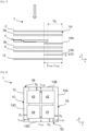
- figure 3 , 5 , 6 And 7 correspond to XZ sections in exploded views of three modes and an alternative embodiment of a photovoltaic module before the lamination step of the manufacturing method according to the invention.
- FIG. 4 corresponds to an XY top view of a particular embodiment of the first embodiment.
- FIG 8 corresponds to an XY top view of a particular embodiment of the third embodiment.
- the photovoltaic module may comprise one or more of the following features.
- the first layer 2, and the fourth layer 12 where appropriate, comprises at least one polymer material.
- the polymer material of the first layer 2 can be chosen from: polycarbonate (PC), polymethyl methacrylate (PMMA), polyethylene terephthalate (PET), polyamide ( PA), a fluorinated polymer, in particular polyvinyl fluoride (PVF) or polyvinylidene fluoride (PVDF), ethylene tetrafluoroethylene (ETFE), ethylene chlorotrifluoroethylene (ECTFE), polytetrafluoroethylene (PTFE), Polychlorotrifluoroethylene (PCTFE ) and/or fluorinated ethylene propylene (FEP).
- PC polycarbonate
- PMMA polymethyl methacrylate
- PET polyethylene terephthalate
- PA polyamide
- a fluorinated polymer in particular polyvinyl fluoride (PVF) or polyvinylidene fluoride (PVDF), ethylene tetrafluoroethylene (ETFE), ethylene chlorotrifluoroethylene (ECTFE), polytetraflu
- the first layer 2 (and the fourth layer 12 if applicable) has a thickness of less than 50 ⁇ m, and advantageously comprised between 5 ⁇ m and 25 ⁇ m.
- the encapsulating assembly 3 (and the fifth layer 13 if applicable) can be made from at least one polymer material chosen from: acid copolymers, ionomers, poly(ethylene-vinyl acetate) (EVA ), vinyl acetals, such as polyvinyl butyrals (PVB), polyurethanes, polyvinyl chlorides, polyethylenes, such as linear low density polyethylenes, elastomeric polyolefin copolymers, copolymers of ⁇ -olefins and ⁇ -, ⁇ - carboxylic to ethylenic acid esters, such as ethylene-methyl acrylate copolymers and ethylene-butyl acrylate copolymers, silicone elastomers and/or epoxy resins.
- polymer material chosen from: acid copolymers, ionomers, poly(ethylene-vinyl acetate) (EVA ), vinyl acetals, such as polyvinyl butyrals (PVB), polyure
- the encapsulating assembly 3 has a total thickness e3 which is less than or equal to 150 ⁇ m, and preferably between 20 and 100 ⁇ m, and even more preferably between 50 ⁇ m and 75 ⁇ m.
- the encapsulant assembly 3 can in particular be made from two layers of polymer material 3a (upper encapsulant layer) and 3b (lower encapsulant layer). he can these may be two layers of poly(ethylene-vinyl acetate) (EVA) or two layers of ionomer, between which the photovoltaic cells 4 are arranged. Each layer 3a, 3b may have a thickness e3a, e3b less than or equal to 75 ⁇ m, and preferably less than or equal to 50 ⁇ m. These layers 3a and 3b, although preferentially of identical nature, can have different optical properties.
- the photovoltaic cells 4 can be chosen from: homojunction or heterojunction photovoltaic cells based on monocrystalline (c-Si) and/or multi-crystalline (mc-Si) silicon, and/or photovoltaic cells of the IBC type, and/or photovoltaic cells comprising at least one material among amorphous silicon (a-Si), microcrystalline silicon ( ⁇ C-Si), cadmium telluride (CdTe), copper-indium selenide (CIS) and copper-indium/gallium diselenide (CIGS) or multi-junction cells (IIVV).
- Their thickness is between 1 and 300 ⁇ m, and in particular between 1 and 200 ⁇ m.
- the photovoltaic cells 4 can have a thickness e4 of between 1 and 300 ⁇ m, in particular between 1 and 250 ⁇ m, or even between 1 and 200 ⁇ m, and advantageously between 70 ⁇ m and 150 ⁇ m.
- the spacing between two neighboring photovoltaic cells, or even consecutive or adjacent can be greater than or equal to 0.5 mm, in particular between 1 and 30 mm, and preferably equal to 2 mm.
- the photovoltaic cells 4 can be interconnected by soldered tinned copper strips.
- the thickness of the photovoltaic cell interconnection ribbons is adapted to be compatible with the lamination process and the low thickness of the encapsulating assembly.
- the cell interconnection ribbons can have a thickness of less than 100 ⁇ m and a width of less than 3 mm.
- the second layer 5 comprises a composite material of the preimpregnated type based on polymer resin and fibers having a surface weight of less than 150 g/m 2 , and advantageously between 50 g/m 2 and 115 g/m 2 . It may for example consist of said at least one composite material.
- the fabric weft of the prepreg may have a basis weight less than or equal to 50 g/m 2 , and the polymer resin impregnation rate may be between 30 and 70% by mass.
- the composite material of the second layer 5 can be a prepreg based on polymer resin and fibers, the polymer being chosen from polyester, epoxy and/or acrylic, and the fibers being chosen from glass fibers, carbon and/or aramid.
- the second layer 5 may in particular have a thickness e5 less than or equal to 100 ⁇ m, in particular between 50 ⁇ m and 80 ⁇ m.
- the third layer 15 (or reinforcement layer) is also made of a composite material of the preimpregnated type based on polymer resin and fibers. This can be one of the materials listed above, with reference to the second layer 5.
- the third layer 15 is the same material as the second layer 5.
- the third layer 15 may in particular have a basis weight of between 50 g/m 2 and 150 g/m 2.
- the third layer may in particular have a thickness e15 of less than or equal to 100 ⁇ m, in particular of between 50 ⁇ m and 80 ⁇ m.
- first layer and/or the second layer of the photovoltaic module can be formed in one or more parts, namely that they can be monolayer or multilayer.
- the first layer 2 and the second layer 5 define the edges of the photovoltaic module 1, and also the encapsulating assembly which extends to the edges of the module.
- the plurality of photovoltaic cells 4 is separated by a distance D A from an edge 1A of the photovoltaic module 1.
- the photovoltaic module 1 also comprises a third layer 15, or reinforcement layer, located below the plurality of photovoltaic cells 4 and above the lower encapsulant layer 3b.
- This third layer forms a peripheral band 15A which extends from edge 1A and overflows below the photovoltaic cell 41 (or photovoltaic cells) closest (the closest) to edge 1A.
- the width L 15A of this peripheral band is thus greater than the distance D A .
- the distance D A can be equal to 50 mm and the width L 15A of the peripheral strip 15A equal to 70 mm. More generally, the difference between the width L 15A and the distance D A is less than or equal to 30 mm, preferably less than or equal to 20 mm, and even more preferably between 10 and 20 mm.
- FIG. 4 is a top view of an exemplary embodiment of the embodiment of the picture 3 .
- the photovoltaic cells are distant from all the edges 1A, 1B, 1C, 1D of the photovoltaic module 1 by a distance D A , D B , D C , D D .
- Four photovoltaic cells 41, 42, 43, 44 are represented but this number is not limiting, and there could be more, or less.
- the third layer 15 forms four peripheral bands 15A, 15B, 15C, 15D, one per edge 1A, 1B, 1C, 1D, thus forming a frame.
- Each peripheral band extending from an edge and overflows below the two photovoltaic cells closest to the edge.
- the width L 15A (resp L 15B , L 15C , L 15D ) of each illustrated peripheral strip is greater than the distance D A (resp D B , D C , D D ) between the edge parallel to said strip and the plurality of cells photovoltaic (4).
- the distances D A , D B , D C , D D can be equal to 50 mm and the widths L 15A , L 15B , L 15C , L 15D of the peripheral bands 15A, 15B, 15C, 15D equal at 70mm.
- the difference between the width L 15A (resp L 15B , L 15C , L 15D ) of strip of the third layer 15 and the distance D A (resp D B , D C , D D ) between the edge parallel to said strip and the cells is less than or equal to 30 mm, preferably less than or equal to 20 mm, and even more preferably between 10 and 20 mm.
- each peripheral strip has the shape of an isosceles trapezium with an angle of 45°.
- the frame may be integral.
- FIG. 5 illustrates, in section and in exploded view, a variant embodiment of the first embodiment.
- the photovoltaic module 1 may include all or part of the characteristics described above, and in particular those related to the figures 3 to 4 which will therefore not be described again.
- the photovoltaic module 1 comprises a fourth layer 12 forming the rear face of the photovoltaic module 1, the second layer 5 being located between the fourth layer 12 and the encapsulating assembly 3.
- This fourth layer 12 is constituted by the same material as that constituting the first layer 2 forming the front face of the photovoltaic module 1.
- this material corresponds to ethylene chlorotrifluoroethylene (ECTFE), also known under the name Halar ® .
- the fourth layer 12 has a lower thickness e12, or equal in this variant of the figure 5 , to the thickness e2 of the first layer 2.
- the fourth layer 12 advantageously makes it possible to achieve dielectric and chemical insulation of the module 1.
- the fourth layer 12 forming the rear face is also represented on the figure 6 And 7 . However, it could be omitted.
- FIG. 6 illustrates, in section and in exploded view, a second embodiment of a photovoltaic module.
- This photovoltaic module of the figure 6 may include all or part of the characteristics described above, and in particular those related to the figures 3 to 5 which will therefore not be described again.
- the upper encapsulant layer (3a) is separated by a distance D 3 from the edge 1A of the photovoltaic module. This distance D 3 is less than the distance D A so that the upper encapsulant layer (3a) can still protect the photovoltaic cells.
- the upper encapsulant layer (3a) may be distant from all the edges of the photovoltaic module, and in particular may be distant by the same distance D 3 from all the edges of the photovoltaic module, as for example in a configuration of the type of figure 4 And 8 .
- the distance D A can be equal to 50 mm, the width L 15A of the peripheral strip 15A equal to 70 mm and the distance D 3 equal to 30 mm.
- the difference between the width L 15A (resp L 15B , L 15C , L 15D ) and the distance D A (resp D B , D C , D D ) is less than or equal to 30 mm, preferably less than or equal to 20 mm, and even more preferably between 10 and 20 mm, and the difference between D A (resp D B , D C , D D ) and D 3 is less than or equal to 10 mm.
- FIG. 7 illustrates, in section and in exploded view, a third embodiment of a photovoltaic module.
- This photovoltaic module of the figure 7 may include all or part of the characteristics described above, and in particular those related to the figures 3 to 5 which will therefore not be described again.
- the photovoltaic module comprises a fifth layer 13 located below the second layer 5 and above the fourth layer 12.
- This fifth layer forms at least one peripheral strip 13A extending from an edge 1A and overflows below the photovoltaic cell 41 (or photovoltaic cells) closest (the closest) to the edge 1A.
- the width L 13A of this peripheral strip is greater than the distance D A .
- This fifth layer 13 is preferably made of the same material as the encapsulating assembly 3.
- the fifth layer is made of a material different from the material of the encapsulating assembly but it must have at least the same thermomechanical properties.
- the advantage of this fifth layer is to symmetrize the edge and/or the edges.
- the distance D A can be equal to 50 mm, the width L 15A of the peripheral strip 15A equal to 70 mm and the width L 13A of the peripheral strip 13A equal to 70 mm.
- the difference between the width L 13A and the distance D A is less than or equal to 30 mm, preferably less than or equal to 20 mm and even more preferably between 10 and 20 mm.
- the width L 13A is equal to the width L 15A .
- FIG 8 corresponds to a bottom view of a particular embodiment of the third embodiment, in which only the fourth layer 12 (from below), the fifth layer 13 and four photovoltaic cells 41, 42, 43 have been shown, 44 (the layers 5, 3b, 15 which are between the layer 13 and the cells are not represented, although present, to make the figure more readable, likewise for the layers above the cells).
- the photovoltaic cells are distant from all the edges 1A, 1B, 1C, 1D of the photovoltaic module 1 by a distance D A , D B , D C , D D .
- Four cells are represented but this number is not limiting, and there could be more, or less.
- the fifth layer 13 can thus form four peripheral bands, one per edge, as for example represented in the configuration of the figure 8 , thus also forming a frame.
- the frame may be in one piece.
- the distances D A , D B , D C , D D can be equal to 50 mm, and the widths L 13A , L 13B , L 13C , L 13D of the peripheral bands 13A, 13B, 13C, 13D equal to 70 mm.
- the difference between the bandwidth L 13A (resp L 13B , L 13C , L 13D ) of the fifth layer and the distance D A (resp D B , D C , D D ) is less than or equal to 30 mm, preferably less than or equal to 20 mm and even more preferably between 10 and 20 mm.
- the width L 13A , (resp L 13B , L 13C , L 13D ) of the band of the fifth layer 13 is equal to the width L 15A , (resp L 15B , L 15C , L 15D ) of the band of the third layer 15.
- the fifth layer 13 is preferably of the same geometric shape as the third layer 15, so that they can overlap.
- the fifth layer 13 may in particular have a thickness e13 less than or equal to 150 ⁇ m, or even less than or equal to 100 ⁇ m.
- the production of a photovoltaic module 1 is carried out in a single hot lamination step, at a temperature of between 130° C. and 170° C., and in particular of the order of 150° C., and for a duration of the cycle of lamination of at least 10 minutes, and in particular between 10 and 20 minutes, of the constituent layers forming the photovoltaic module 1.
Description
La présente invention se rapporte au domaine des modules photovoltaïques, qui comportent un ensemble de cellules photovoltaïques reliées entre elles électriquement, et préférentiellement des cellules photovoltaïques dites « cristallines », c'est-à-dire qui sont à base de silicium monocristallin ou multicristallin.The present invention relates to the field of photovoltaic modules, which comprise a set of photovoltaic cells interconnected electrically, and preferably so-called “crystalline” photovoltaic cells, that is to say which are based on monocrystalline or multicrystalline silicon.
Plus précisément, la présente invention se rapporte au domaine des modules photovoltaïques ultra-légers (poids surfacique inférieur à 1 kg/m2 voire inférieur à 800 g/m2, voire encore inférieur à 600 g/m2) et flexibles.More specifically, the present invention relates to the field of ultra-light photovoltaic modules (area weight less than 1 kg/m 2 or even less than 800 g/m 2 , or even even less than 600 g/m 2 ) and flexible.
L'invention peut être mise en oeuvre pour de nombreuses applications, par exemple des applications autonomes et/ou embarquées, étant particulièrement concernée par les applications qui requièrent l'utilisation de modules photovoltaïques flexibles, sans verre et ultra-légers, en particulier d'un poids par unité de surface inférieur à 1 kg/m2, et notamment inférieur à 800 g/m2, voire encore inférieur à 600 g/m2, et de faible épaisseur, notamment inférieure à 1 mm. Elle peut ainsi notamment être appliquée pour des bâtiments tels que des habitats ou locaux industriels (tertiaires, commerciaux,...), par exemple pour la réalisation de leurs toitures, pour la conception de mobilier urbain, par exemple pour de l'éclairage public, la signalisation routière ou encore la recharge de voitures électriques, voire également être utilisée pour des applications nomades, en particulier pour une intégration sur des objets volants, des voitures, bus ou bateaux, entre autres.The invention can be implemented for numerous applications, for example autonomous and/or on-board applications, being particularly concerned with applications which require the use of flexible, glassless and ultra-light photovoltaic modules, in particular a weight per unit area of less than 1 kg/m 2 , and in particular less than 800 g/m 2 , or even less than 600 g/m 2 , and of low thickness, in particular less than 1 mm. It can thus in particular be applied to buildings such as housing or industrial premises (tertiary, commercial, etc.), for example for the construction of their roofs, for the design of street furniture, for example for public lighting. , road signs or electric car charging, or even be used for nomadic applications, in particular for integration on flying objects, cars, buses or boats, among others.
Un module photovoltaïque est un assemblage de cellules photovoltaïques disposées côte à côte entre une première couche formant une face avant du module photovoltaïque et une seconde couche formant une face arrière du module photovoltaïque. La première couche formant la face avant du module photovoltaïque est transparente pour permettre aux cellules photovoltaïques de recevoir un flux lumineux.A photovoltaic module is an assembly of photovoltaic cells arranged side by side between a first layer forming a front face of the photovoltaic module and a second layer forming a rear face of the photovoltaic module. The first layer forming the front face of the photovoltaic module is transparent to allow the photovoltaic cells to receive a luminous flux.
Les cellules photovoltaïques peuvent être reliées électriquement entre elles par des éléments de contact électrique avant et arrière, appelés conducteurs de liaison, et formés par exemple par des bandes de cuivre étamé, respectivement disposées contre les faces avant (faces se trouvant en regard de la face avant du module photovoltaïque destinée à recevoir un flux lumineux) et arrière (faces se trouvant en regard de la face arrière du module photovoltaïque) de chacune des cellules photovoltaïques, ou bien encore uniquement en face arrière pour les cellules photovoltaïques de type IBC (pour « Interdigitated Back Contact » en anglais).The photovoltaic cells can be electrically connected to each other by front and rear electrical contact elements, called connecting conductors, and formed for example by strips of tinned copper, respectively arranged against the front faces (faces facing the face of the photovoltaic module intended to receive a luminous flux) and rear (faces facing the rear face of the photovoltaic module) of each of the photovoltaic cells, or even only on the rear face for IBC type photovoltaic cells (for " Interdigitated Back Contact” in English).
Par ailleurs, les cellules photovoltaïques, situées entre les première et deuxième couches formant respectivement les faces avant et arrière du module photovoltaïque, peuvent être encapsulées.Furthermore, the photovoltaic cells, located between the first and second layers respectively forming the front and rear faces of the photovoltaic module, can be encapsulated.
La demande de
- une première couche transparente 2, formant la face avant du module photovoltaïque, et comportant au moins un matériau polymère et présente une épaisseur e2 inférieure à 50 µm ;
- la
deuxième couche 5, pouvant former la face arrière du module photovoltaïque, comportant au moins un matériau composite de type préimprégné à base de résine polymère et de fibres, et présentant un poids surfacique inférieur à 150 g/m2 ; - une pluralité de cellules photovoltaïques 4 disposées côte à côte et reliées électriquement entre elles par des éléments de contact électrique sous forme de rubans d'interconnexion,
- un ensemble 3 (formé par deux
couches 3a et 3b) encapsulant la pluralité de cellules photovoltaïques et présentant une épaisseur maximale e3 inférieure à 150 µm ; l'ensemble encapsulant et la pluralité de cellules photovoltaïques étant situés entre les première et deuxième couches.
- a first
transparent layer 2, forming the front face of the photovoltaic module, and comprising at least one polymer material and has a thickness e2 of less than 50 μm; - the
second layer 5, which can form the rear face of the photovoltaic module, comprising at least one composite material of the preimpregnated type based on polymer resin and fibers, and having a surface weight of less than 150 g/m 2 ; - a plurality of
photovoltaic cells 4 arranged side by side and electrically interconnected by electrical contact elements in the form of interconnecting ribbons, - an assembly 3 (formed by two
layers
La flèche correspond au rayonnement lumineux qui arrive sur la première couche transparente 2, formant la face avant du module photovoltaïque.The arrow corresponds to the light radiation which arrives at the first
La réalisation du module photovoltaïque 1 est effectuée en une seule étape de lamination à chaud, à une température comprise entre 130°C et 170°C et pendant une durée du cycle de lamination d'au moins 10 minutes des couches constitutives 2, 3, 4, 5 formant le module photovoltaïque 1. The production of the
Comme illustré en
En d'autres termes, les cellules photovoltaïques sont distantes des bords du module formés par les première et deuxième couches ainsi que par l'ensemble encapsulant les cellules photovoltaïques (distance égale à la valeur du débord D). Ceci permet de protéger au mieux lesdites cellules, sur laquelle le module photovoltaïque comprend en outre en face arrière une couche additionnelle 10 constituée par le même matériau que celui constituant la première couche 2 formant la face avant du module photovoltaïque 1.In other words, the photovoltaic cells are distant from the edges of the module formed by the first and second layers as well as by the assembly encapsulating the photovoltaic cells (distance equal to the value of the overhang D ). This makes it possible to best protect said cells, on which the photovoltaic module further comprises on the rear face an
La
L'ensemble encapsulant doit généralement présenter un débord d'au moins 16 mm (depuis le bord du dernier conducteur électrique, cellule ou ruban d'interconnexion) voire davantage, pour assurer l'isolation électrique lorsque l'opération de lamination est réalisée, si le module est soumis à une tension de fonctionnement de 1000 V. Ce débord permet aussi d'assurer l'étanchéité hydrique et chimique du module. Les première et deuxième couches suivent les dimensions de l'ensemble encapsulant. Ce débord peut être plus faible si les matériaux utilisés ont des rigidités électriques très élevées, si la tension de fonctionnement du module est plus faible ou bien si les conditions environnementales d'utilisation du module ne nécessitent pas une étanchéité hydrique ou chimique élevée. Dans tous les cas, pour des raisons de facilité de procédé, le débord est très souvent d'au moins 5 mm.The encapsulating assembly must generally have an overhang of at least 16 mm (from the edge of the last electrical conductor, cell or interconnect ribbon) or even more, to ensure electrical insulation when the lamination operation is carried out, if the module is subjected to an operating voltage of 1000 V. This overhang also ensures the water and chemical seal of the module. The first and second layers follow the dimensions of the encapsulating assembly. This overhang may be lower if the materials used have very high electrical rigidities, if the operating voltage of the module is lower or if the environmental conditions of use of the module do not require high water or chemical sealing. In all cases, for reasons of ease of process, the overhang is very often at least 5 mm.
En outre, certaines applications de ces modules photovoltaïques ultra-légers (par exemple pour une intégration sur un objet volant) supposent souvent de les fixer à un objet par l'intermédiaire de moyens de fixation disposés au niveau des bords du module, et non par l'intermédiaire de la face arrière comme cela peut être le cas pour d'autres modules photovoltaïques et/ou d'autres applications.In addition, certain applications of these ultra-light photovoltaic modules (for example for integration on a flying object) often involve fixing them to an object by means of fixing means arranged at the edges of the module, and not by via the rear face as may be the case for other photovoltaic modules and/or other applications.
Or les inventeurs ont constaté que pour un module photovoltaïque ultra-léger tel que précédemment décrit, les contraintes internes après lamination, liées à la dissymétrie de la structure obtenue, conduisent à une courbure sur les bords du module. Les courbures peuvent alors compliquer, gêner voire empêcher l'utilisation des moyens de fixation susmentionnés. Les courbures peuvent en outre présenter des risques d'accrochages ou des problèmes de prise au vent, voire des défauts esthétiques qui ne sont pas compatibles avec certaines applications.However, the inventors have observed that for an ultra-light photovoltaic module as described above, the internal stresses after lamination, linked to the asymmetry of the structure obtained, lead to a curvature on the edges of the module. The curvatures can then complicate, hamper or even prevent the use of the aforementioned fixing means. Curvatures may also present risks of snagging or problems of wind resistance, or even aesthetic defects which are not compatible with certain applications.
L'invention vise à surmonter les inconvénients précités de l'art antérieur.The invention aims to overcome the aforementioned drawbacks of the prior art.
Plus particulièrement, l'invention vise à disposer d'un module photovoltaïque ultra-léger et flexible dont les bords ne présentent pas ou peu de courbure, tout en présentant des propriétés mécaniques et des performances électriques au moins équivalentes à celles des modules photovoltaïques ultra-légers et flexibles de l'art antérieur. En d'autres termes, l'invention vise à obtenir des modules photovoltaïques ultra-légers et flexibles les plus plats possibles.More particularly, the invention aims to have an ultra-light and flexible photovoltaic module whose edges have little or no curvature, while having mechanical properties and electrical performance at least equivalent to those of ultra-light photovoltaic modules. lightweight and flexible prior art. In other words, the invention aims to obtain ultra-light and flexible photovoltaic modules that are as flat as possible.
Le document
Un premier objet de l'invention permettant de remédier à ces inconvénients est un module photovoltaïque comportant :
- une première couche transparente formant la face avant du module photovoltaïque destinée à recevoir un flux lumineux,
- une pluralité de cellules photovoltaïques disposées côte à côte et reliées électriquement entre elles,
- un ensemble encapsulant apte à encapsuler la pluralité de cellules photovoltaïques, présentant une partie inférieure et une partie supérieure, l'ensemble encapsulant étant de préférence en polymère,
- une deuxième couche comportant au moins un matériau composite à base de résine polymère et de fibres, l'ensemble encapsulant et la pluralité de cellules photovoltaïques étant situés entre les première et deuxième couches,
- a first transparent layer forming the front face of the photovoltaic module intended to receive a luminous flux,
- a plurality of photovoltaic cells arranged side by side and electrically connected together,
- an encapsulating assembly capable of encapsulating the plurality of photovoltaic cells, having a lower part and an upper part, the encapsulating assembly preferably being made of polymer,
- a second layer comprising at least one composite material based on polymer resin and fibers, the encapsulating assembly and the plurality of photovoltaic cells being located between the first and second layers,
De préférence, l'écart entre la largeur de la au moins une bande périphérique et la distance DA entre la pluralité de cellules photovoltaïques et le au moins un bord est inférieur ou égale à 30 mm, encore plus préférentiellement inférieur ou égale à 20 mm.Preferably, the difference between the width of the at least one peripheral band and the distance D A between the plurality of photovoltaic cells and the at least one edge is less than or equal to 30 mm, even more preferably less than or equal to 20 mm .
De préférence, la largeur de la au moins une bande périphérique de la troisième couche est strictement supérieure à la au moins une distance entre les cellules photovoltaïques et le au moins un bordPreferably, the width of the at least one peripheral band of the third layer is strictly greater than the at least one distance between the photovoltaic cells and the at least one edge
De préférence, la deuxième couche est en un matériau préimprégné à base de résine polymère et de fibres.Preferably, the second layer is made of a preimpregnated material based on polymer resin and fibers.
De préférence, la troisième couche est en un matériau préimprégné à base de résine polymère et de fibres.Preferably, the third layer is made of a preimpregnated material based on polymer resin and fibers.
Par « bande », il faut comprendre un élément s'étendant longitudinalement selon la direction du bord et dont la largeur est définie perpendiculairement à la direction du bord dans le plan du module photovoltaïque.By “strip”, it is necessary to understand an element extending longitudinally in the direction of the edge and whose width is defined perpendicular to the direction of the edge in the plane of the photovoltaic module.
Une bande est dite « périphérique » en ce qu'elle est disposée au niveau d'un bord du module photovoltaïque. Ainsi, une bande périphérique est disposée depuis un bord de la cellule photovoltaïque et atteint, voire déborde sous, la (ou les) cellule(s) photovoltaïque(s) le(s) plus proche(s) du bord.A strip is said to be “peripheral” in that it is placed at one edge of the photovoltaic module. Thus, a peripheral band is arranged from an edge of the photovoltaic cell and reaches, or even overflows under, the photovoltaic cell(s) closest to the edge.
La « distance » entre un bord et la pluralité de cellules photovoltaïques sous-entend la distance la plus courte entre ledit bord et la (ou les) cellule(s) photovoltaïque(s) le(s) plus proche(s) du bord.The “distance” between an edge and the plurality of photovoltaic cells implies the shortest distance between said edge and the photovoltaic cell(s) closest to the edge.
Les distances entre tous les bords du module photovoltaïque et la pluralité de cellules photovoltaïques peuvent être toutes identiques. Dans ce cas, les largeurs de bandes périphériques peuvent être toutes identiques également.The distances between all the edges of the photovoltaic module and the plurality of photovoltaic cells can all be identical. In this case, the peripheral band widths can all be identical as well.
Les épaisseurs des cellules et des différentes couches, et notamment des bandes périphériques, sont définies selon la direction perpendiculaire au plan du module photovoltaïque.The thicknesses of the cells and of the various layers, and in particular of the peripheral bands, are defined according to the direction perpendicular to the plane of the photovoltaic module.
Le terme « transparent » signifie que le matériau de la première couche formant la face avant du module photovoltaïque est au moins partiellement transparent à la lumière visible, laissant passer au moins environ 80 % de cette lumière.The term “transparent” means that the material of the first layer forming the front face of the photovoltaic module is at least partially transparent to visible light, allowing at least approximately 80% of this light to pass.
La « face avant » du module photovoltaïque correspond à la face destinée à recevoir un flux lumineux. Elle peut être désignée par « face supérieure ». La « face arrière » correspond à la face opposée dudit module. Elle peut être désignée par « face inférieure ». Les termes « en dessous » et « inférieur » sont à comprendre par référence à la face arrière du module photovoltaïque. A l'inverse, le terme « au-dessus » et « supérieur » sont à comprendre par référence à la face avant du module photovoltaïque.The "front face" of the photovoltaic module corresponds to the face intended to receive a luminous flux. It may be referred to as the “upper face”. The “rear face” corresponds to the opposite face of said module. It may be referred to as the “underside”. The terms "below" and "lower" are to be understood with reference to the rear face of the photovoltaic module. Conversely, the term “above” and “upper” are to be understood by reference to the front face of the photovoltaic module.
En outre, par le terme «encapsulant » ou « encapsulé », il faut comprendre que la pluralité de cellules photovoltaïques est disposée dans un volume, par exemple hermétiquement étanche vis-à-vis des liquides, au moins en partie formé par au moins deux couches de matériau(x) d'encapsulation, réunies entre elles après lamination pour former l'ensemble encapsulant.In addition, by the term “encapsulating” or “encapsulated”, it should be understood that the plurality of photovoltaic cells is arranged in a volume, for example hermetically sealed with respect to liquids, at least partly formed by at least two layers of encapsulating material(s), joined together after lamination to form the encapsulating assembly.
En effet, initialement, c'est-à-dire avant toute opération de lamination, l'ensemble encapsulant est constitué par au moins deux couches de matériau(x) d'encapsulation, dites couches de coeur, entre lesquelles la pluralité de cellules photovoltaïques est encapsulée. Toutefois, pendant l'opération de lamination des couches, les couches de matériau d'encapsulation fondent pour ne former, après l'opération de lamination, qu'une seule couche (ou ensemble) solidifiée dans laquelle sont noyées les cellules photovoltaïques.Indeed, initially, that is to say before any lamination operation, the encapsulating assembly consists of at least two layers of encapsulating material(s), called core layers, between which the plurality of photovoltaic cells is encapsulated. However, during the layer lamination operation, the layers of encapsulation material melt to form, after the lamination operation, only a single solidified layer (or assembly) in which the photovoltaic cells are embedded.
Ainsi l'invention vise à améliorer la symétrie des matériaux dans les zones sans cellules photovoltaïques et éventuellement sans rubans inter-connecteurs, en ajoutant une ou plusieurs bandes périphériques (couche de renforcement) uniquement dans ces zones et/ou en modifiant d'autres couches constitutives du module. Cela permet d'éviter la création de courbures sur les bords du module photovoltaïque.Thus the invention aims to improve the symmetry of the materials in the zones without photovoltaic cells and possibly without inter-connector strips, by adding one or more peripheral bands (reinforcing layer) only in these zones and/or by modifying other constituent layers of the module. This avoids the creation of curvatures on the edges of the photovoltaic module.
Ces bandes périphériques peuvent être dans des matériaux constitutifs des couches déjà présentes dans le module photovoltaïque, comme le matériau composite à base de résine polymère et de fibres de la deuxième couche. Ces bandes périphériques localisées sur les bords ont pour but de symétriser la structure du module photovoltaïque au niveau des bords, et au mieux d'en améliorer la symétrie, tout en respectant les autres contraintes en fonction de l'application visée du module photovoltaïque.These peripheral bands can be in materials constituting the layers already present in the photovoltaic module, such as the composite material based on polymer resin and fibers of the second layer. The purpose of these peripheral bands located on the edges is to symmetrize the structure of the photovoltaic module at the edges, and at best to improve its symmetry, while respecting the other constraints depending on the intended application of the photovoltaic module.
Une solution évidente aurait été, partant du module photovoltaïque de la
Ces bandes périphériques permettent ainsi de former un module photovoltaïque ultra-léger et plat, sans courbure, facilitant l'utilisation d'un système de fixation du module photovoltaïque, et ce, sans augmenter considérablement le poids par unité de surface et le prix de revient d'un tel module.These peripheral strips thus make it possible to form an ultra-light and flat photovoltaic module, without curvature, facilitating the use of a system for fixing the photovoltaic module, and this, without considerably increasing the weight per unit area and the cost price. of such a module.
Le module photovoltaïque selon l'invention peut en outre comporter l'une ou plusieurs des caractéristiques suivantes prises isolément ou suivant toutes combinaisons techniques possibles. En d'autres termes, les modes de réalisation indiqués dans ce qui suit peuvent être combinés entre eux, sauf lorsqu'il s'agit explicitement d'un mode alternatif à un autre.The photovoltaic module according to the invention may further comprise one or more of the following characteristics taken individually or in any possible technical combination. In other words, the embodiments indicated in the following can be combined with each other, except when it is explicitly an alternative mode to another.
Selon un mode de réalisation, la troisième couche et/ou la deuxième couche est en matériau composite à base de polymère et de fibres, le polymère étant choisi de préférence parmi le polyester, l'époxy et/ou l'acrylique ; et/ou les fibres étant choisies de préférence parmi les fibres de verre, de carbone et/ou d'aramide.According to one embodiment, the third layer and/or the second layer is made of a composite material based on polymer and fibers, the polymer preferably being chosen from polyester, epoxy and/or acrylic; and/or the fibers being preferably chosen from glass, carbon and/or aramid fibres.
Selon un mode de réalisation préféré, la troisième couche est en le même matériau composite que la deuxième couche.According to a preferred embodiment, the third layer is made of the same composite material as the second layer.
Selon un mode de réalisation particulier, la troisième couche forme plusieurs bandes périphériques, de préférence au moins deux bandes opposées, et encore plus préférentiellement quatre bandes, chaque bande périphérique s'étendant depuis un bord du module photovoltaïque vers le centre dudit module, la largeur de chaque bande périphérique étant supérieure ou égale à la distance DA, DB,According to a particular embodiment, the third layer forms several peripheral bands, preferably at least two opposite bands, and even more preferably four bands, each peripheral band extending from an edge of the photovoltaic module towards the center of said module, the width of each peripheral strip being greater than or equal to the distance D A , D B ,
DC, DD entre ledit bord et la pluralité de cellules photovoltaïques. De préférence, l'écart entre la largeur de chaque bande périphérique et la distance DA, DB, DC, DD est inférieur ou égal à 30 mm, et encore plus préférentiellement inférieur ou égal à 20 mm.D C , D D between said edge and the plurality of photovoltaic cells. Preferably, the gap between the width of each peripheral strip and the distance D A , D B , D C , D D is less than or equal to 30 mm, and even more preferably less than or equal to 20 mm.
De préférence, la largeur de chaque bande périphérique de la troisième couche est strictement supérieure à la distance DA, DB, DC, DD.Preferably, the width of each peripheral band of the third layer is strictly greater than the distance D A , D B , D C , D D .
Selon un mode de réalisation, l'ensemble encapsulant s'étend jusqu'aux bords du module photovoltaïque.According to one embodiment, the encapsulating assembly extends to the edges of the photovoltaic module.
Selon un mode de réalisation alternatif au mode précédent, la partie supérieure de l'ensemble encapsulant est espacée d'une distance D3A du au moins un bord du module photovoltaïque, la distance D3A étant non nulle et inférieure à la distance DA entre ledit au moins un bord et la pluralité de cellules photovoltaïques, l'écart entre lesdites distances DA et D3A étant de préférence inférieur ou égal à 10 mm. En particulier, la partie supérieure de l'ensemble encapsulant peut-être espacée d'une distance D3A, D3B, D3C, D3D non nulle de chaque bord du module photovoltaïque, l'écart entre la distance D3A, D3B, D3C, D3D et la distance DA, DB, DC, DD entre ledit bord et la pluralité de cellules photovoltaïques étant de préférence inférieur ou égal à 10 mm.According to an alternative embodiment to the previous mode, the upper part of the encapsulating assembly is spaced by a distance D 3A from at least one edge of the photovoltaic module, the distance D 3A being non-zero and less than the distance D A between said at least one edge and the plurality of photovoltaic cells, the difference between said distances D A and D 3A preferably being less than or equal to 10 mm. In particular, the upper part of the encapsulating assembly may be spaced apart by a non-zero distance D 3A , D 3B , D 3C , D 3D from each edge of the photovoltaic module, the difference between the distance D 3A , D 3B , D 3C , D 3D and the distance D A , D B , D C , D D between said edge and the plurality of photovoltaic cells preferably being less than or equal to 10 mm.
Selon un mode de réalisation, le module photovoltaïque comprend en outre une cinquième couche, de préférence en polymère, située en dessous de la deuxième couche, ladite cinquième couche formant au moins une bande périphérique s'étendant depuis le au moins un bord vers le centre dudit module et dont la largeur est supérieure ou égale à la distance DA entre ledit au moins un bord et la pluralité de cellules photovoltaïques. De préférence, l'écart entre ladite largeur et ladite distance est inférieur ou égal à 30 mm, et encore plus préférentiellement inférieur ou égal à 20 mm.According to one embodiment, the photovoltaic module further comprises a fifth layer, preferably made of polymer, located below the second layer, said fifth layer forming at least one peripheral band extending from the at least one edge towards the center said module and whose width is greater than or equal to the distance D A between said at least one edge and the plurality of photovoltaic cells. Preferably, the difference between said width and said distance is less than or equal to 30 mm, and even more preferably less than or equal to 20 mm.
Selon un mode de réalisation particulier, la cinquième couche forme plusieurs bandes périphériques, de préférence au moins deux bandes opposées, et encore plus préférentiellement quatre bandes, chaque bande périphérique s'étendant depuis un bord du module photovoltaïque vers le centre dudit module et la largeur de chaque bande périphérique étant supérieure ou égale à la distance DA, DB, DC, DD entre ledit bord et la pluralité de cellules photovoltaïques. De préférence, l'écart entre la largeur de chaque bande périphérique et la distance DA, DB, DC, DD est inférieur ou égal à 30 mm, et encore plus préférentiellement inférieur ou égal à 20 mm.According to a particular embodiment, the fifth layer forms several peripheral bands, preferably at least two opposite bands, and even more preferably four bands, each peripheral band extending from an edge of the photovoltaic module towards the center of said module and the width of each peripheral band being greater than or equal to the distance D A , D B , D C , D D between said edge and the plurality of photovoltaic cells. Preferably, the difference between the width of each peripheral strip and the distance D A , D B , D C , D D is less than or equal to 30 mm, and even more preferably less than or equal to 20 mm.
De préférence, la largeur de chaque bande périphérique de la cinquième couche est strictement supérieure à la distance DA, DB, DC, DD.Preferably, the width of each peripheral band of the fifth layer is strictly greater than the distance D A , D B , D C , D D .
Ladite cinquième couche est de préférence en le même polymère que le matériau de l'ensemble encapsulant, ou au moins un polymère ayant les mêmes propriétés thermomécaniques.Said fifth layer is preferably made of the same polymer as the material of the encapsulating assembly, or at least one polymer having the same thermomechanical properties.
Selon un mode de réalisation particulier, les dimensions de la cinquième couche sont sensiblement égales aux dimensions de la troisième couche.According to a particular embodiment, the dimensions of the fifth layer are substantially equal to the dimensions of the third layer.
Selon un mode de réalisation, le module photovoltaïque comprend en outre :
- une quatrième couche formant la face arrière du module photovoltaïque, la deuxième couche étant située entre l'ensemble encapsulant et ladite quatrième couche, ladite quatrième couche étant constituée par le même matériau que celui constituant la première couche, et présentant une épaisseur inférieure ou égale à celle de la première couche.
- a fourth layer forming the rear face of the photovoltaic module, the second layer being located between the encapsulating assembly and said fourth layer, said fourth layer being constituted by the same material as that constituting the first layer, and having a thickness less than or equal to that of the first layer.
Le module photovoltaïque peut en outre présenter les caractéristiques additionnelles suivantes prises isolément ou en combinaison les unes avec les autres, ainsi qu'avec une ou plusieurs des caractéristiques précédentes :
- la première couche est en un matériau polymère ;
- la première couche présente une épaisseur inférieure ou égale à 50 µm ;
- l'ensemble encapsulant présente une épaisseur maximale inférieure à 150 µm ;
- la deuxième couche présente un poids surfacique inférieur à 150 g/m2 ;
- l'ensemble encapsulant comprend une couche supérieure d'encapsulant disposée entre la première couche et la pluralité de cellules photovoltaïques et une couche inférieure d'encapsulant disposée entre la pluralité de cellules photovoltaïques et la deuxième couche.
- the first layer is made of a polymer material;
- the first layer has a thickness less than or equal to 50 μm;
- the encapsulating assembly has a maximum thickness of less than 150 μm;
- the second layer has a surface weight of less than 150 g/m 2 ;
- the encapsulant assembly includes an upper encapsulant layer disposed between the first layer and the plurality of photovoltaic cells and a lower encapsulant layer disposed between the plurality of photovoltaic cells and the second layer.
Un deuxième objet de l'invention est un procédé de réalisation d'un tel module photovoltaïque comportant au moins une étape de lamination à chaud, à une température comprise entre 130°C et 170°C, notamment de l'ordre de 150°C, et pendant une durée du cycle de lamination d'au moins 10 minutes, notamment comprise entre 10 et 20 minutes, des couches constitutives du module photovoltaïque.A second object of the invention is a method for producing such a photovoltaic module comprising at least one hot lamination step, at a temperature between 130° C. and 170° C., in particular of the order of 150° C. , and for a duration of the lamination cycle of at least 10 minutes, in particular between 10 and 20 minutes, of the constituent layers of the photovoltaic module.
Le module photovoltaïque et le procédé de réalisation selon l'invention peuvent comporter l'une quelconque des caractéristiques précédemment énoncées, prises isolément ou selon toutes combinaisons techniquement possibles avec d'autres caractéristiques.The photovoltaic module and the production method according to the invention may include any of the characteristics listed above, taken in isolation or according to any technically possible combination with other characteristics.
D'autres caractéristiques et avantages de l'invention apparaîtront à l'aide de la description qui suit, donnée à titre illustratif et non limitatif, faite en regard des figures annexées parmi lesquelles
- [
Fig.1 ] représente un module photovoltaïque de l'art antérieur. - [
Fig.2 ] représente un module photovoltaïque particulier de l'art antérieur. - [
Fig.3 ] illustre, en coupe et en vue éclatée, un premier mode de réalisation d'un module photovoltaïque conforme à l'invention. - [
Fig.4 ] illustre, en vue de dessus, un exemple de réalisation particulier du premier mode de réalisation d'un module photovoltaïque conforme à l'invention. - [
Fig.5 ] illustre, en coupe et en vue éclatée, une variante du premier mode de réalisation d'un module photovoltaïque conforme à l'invention. - [
Fig.6 ] illustre, en coupe et en vue éclatée, un deuxième mode de réalisation d'un module photovoltaïque conforme à l'invention. - [
Fig.7 ] illustre, en coupe et en vue éclatée, un troisième mode de réalisation d'un module photovoltaïque conforme à l'invention. - [
Fig.8 ] illustre, en vue de dessous, un exemple de réalisation particulier du troisième mode de réalisation d'un module photovoltaïque conforme à l'invention.
- [
Fig.1 ] represents a photovoltaic module of the prior art. - [
Fig.2 ] represents a particular photovoltaic module of the prior art. - [
Fig.3 ] illustrates, in section and in exploded view, a first embodiment of a photovoltaic module according to the invention. - [
Fig.4 ] illustrates, in top view, a particular embodiment of the first embodiment of a photovoltaic module according to the invention. - [
Fig.5 ] illustrates, in section and in exploded view, a variant of the first embodiment of a photovoltaic module according to the invention. - [
Fig.6 ] illustrates, in section and in exploded view, a second embodiment of a photovoltaic module according to the invention. - [
Fig.7 ] illustrates, in section and in exploded view, a third embodiment of a photovoltaic module according to the invention. - [
Fig.8 ] illustrates, in bottom view, a particular embodiment of the third embodiment of a photovoltaic module according to the invention.
Dans l'ensemble de ces figures, des références identiques peuvent désigner des éléments identiques ou analogues.In all of these figures, identical references can designate identical or similar elements.
De plus, les différentes parties représentées sur les figures ne le sont pas nécessairement selon une échelle uniforme, pour rendre les figures plus lisibles.In addition, the different parts shown in the figures are not necessarily shown on a uniform scale, to make the figures more readable.
Les
Dans l'ensemble des figures en coupe, la flèche correspond au rayonnement lumineux.In all of the sectional figures, the arrow corresponds to the light radiation.
Il est à noter que les
La
La
Dans l'ensemble des
De préférence, la première couche 2, et la quatrième couche 12 le cas échéant, comporte au moins un matériau polymère.Preferably, the
Le matériau polymère de la première couche 2 (et de la quatrième couche 12 le cas échéant) peut être choisi parmi : le polycarbonate (PC), le polyméthacrylate de méthyle (PMMA), le polytéréphtalate d'éthylène (PET), le polyamide (PA), un polymère fluoré, notamment le polyfluorure de vinyle (PVF) ou le polyfluorure de vinylidène (PVDF), l'éthylène tétrafluoroéthylène (ETFE), l'éthylène chlorotrifluoroéthylène (ECTFE), le polytétrafluoroéthylène (PTFE), le Polychlorotrifluoroéthylène (PCTFE) et/ou l'éthylène propylène fluoré (FEP).The polymer material of the first layer 2 (and of the
La première couche 2 (et la quatrième couche 12 le cas échéant) présente une épaisseur inférieure à 50 µm, et avantageusement comprise entre 5µm et 25 µm.The first layer 2 (and the
L'ensemble encapsulant 3 (et la cinquième couche 13 le cas échéant) peut être réalisé à partir d'au moins un matériau polymère choisi parmi : les copolymères d'acides, les ionomères, le poly(éthylène-acétate de vinyle) (EVA), les acétals de vinyle, tels que les polyvinylbutyrals (PVB), les polyuréthanes, les chlorures de polyvinyle, les polyéthylènes, tels que les polyéthylènes linéaires basse densité, les polyoléfines élastomères de copolymères, les copolymères d'a-oléfines et des α-, β- esters d'acide carboxylique à éthylénique, tels que les copolymères éthylène-acrylate de méthyle et les copolymères éthylène-acrylate de butyle, les élastomères de silicone et/ou les résines époxy.The encapsulating assembly 3 (and the fifth layer 13 if applicable) can be made from at least one polymer material chosen from: acid copolymers, ionomers, poly(ethylene-vinyl acetate) (EVA ), vinyl acetals, such as polyvinyl butyrals (PVB), polyurethanes, polyvinyl chlorides, polyethylenes, such as linear low density polyethylenes, elastomeric polyolefin copolymers, copolymers of α-olefins and α -, β- carboxylic to ethylenic acid esters, such as ethylene-methyl acrylate copolymers and ethylene-butyl acrylate copolymers, silicone elastomers and/or epoxy resins.
L'ensemble encapsulant 3 présente une épaisseur totale e3 qui est inférieure ou égale à 150 µm, et préférentiellement comprise entre 20 et 100 µm, et encore préférentiellement comprise entre 50 µm et 75 µm.The encapsulating
L'ensemble encapsulant 3 peut notamment être réalisé à partir de deux couches en matériau polymère 3a (couche d'encapsulant supérieure) et 3b (couche d'encapsulant inférieure). Il peut s'agir de deux couches de poly(éthylène-acétate de vinyle) (EVA) ou deux couches de ionomère, entre lesquelles sont disposées les cellules photovoltaïques 4. Chaque couche 3a, 3b peut présenter une épaisseur e3a, e3b inférieure ou égale à 75 µm, et de préférence inférieure ou égale à 50 µm. Ces couches 3a et 3b, bien que préférentiellement de nature identique, peuvent avoir des propriétés optiques différentes.The
Les cellules photovoltaïques 4 peuvent être choisies parmi : des cellules photovoltaïques homojonction ou hétérojonction à base de silicium monocristallin (c-Si) et/ou multi-cristallin (mc-Si), et/ou des cellules photovoltaïques de type IBC, et/ou des cellules photovoltaïques comprenant au moins un matériau parmi le silicium amorphe (a-Si), le silicium microcristallin (µC-Si), le tellurure de cadmium (CdTe), le cuivre-indium séléniure (CIS) et le cuivre-indium/gallium diséléniure (CIGS) ou bien des cellules multi-jonctions (IIVV). Leur épaisseur est comprise entre 1 et 300µm, et notamment entre 1 et 200µm.The
Les cellules photovoltaïques 4 peuvent présenter une épaisseur e4 comprise entre 1 et 300 µm, notamment entre 1 et 250 µm, voire entre 1 et 200 µm, et avantageusement entre 70 µm et 150 µm.The
En outre, l'espacement entre deux cellules photovoltaïques voisines, ou encore consécutives ou adjacentes, peut être supérieur ou égal à 0,5 mm, notamment compris entre 1 et 30 mm, et de préférence égal à 2 mm.In addition, the spacing between two neighboring photovoltaic cells, or even consecutive or adjacent, can be greater than or equal to 0.5 mm, in particular between 1 and 30 mm, and preferably equal to 2 mm.
En outre, les cellules photovoltaïques 4 peuvent être interconnectées par des rubans en cuivre étamé soudés. L'épaisseur des rubans d'interconnexion des cellules photovoltaïques est adaptée pour être compatible avec le procédé de lamination et la faible épaisseur de l'ensemble encapsulant. Les rubans d'interconnexion des cellules peuvent présenter une épaisseur inférieure à 100 µm et une largeur inférieure à 3 mm.Furthermore, the
La deuxième couche 5 comprend un matériau composite de type préimprégné à base de résine polymère et de fibres présentant un poids surfacique inférieur à 150 g/m2, et avantageusement compris entre 50 g/m2 et 115 g/m2. Elle peut être par exemple constituée par ledit au moins un matériau composite. La trame en tissu du préimprégné peut avoir un grammage inférieur ou égal à 50 g/m2, et le taux d'imprégnation de résine polymère peut être compris entre 30 et 70 % en masse.The
Le matériau composite de la deuxième couche 5 peut être un préimprégné à base de résine polymère et de fibres, le polymère étant choisi parmi le polyester, l'époxy et/ou l'acrylique, et les fibres étant choisies parmi les fibres de verre, de carbone et/ou d'aramide.The composite material of the
La deuxième couche 5 peut en particulier présenter une épaisseur e5 inférieure ou égale à 100 µm, notamment comprise entre 50 µm et 80 µm.The
Dans les modes de réalisation représentés, la troisième couche 15 (ou couche de renforcement) est également en un matériau composite de type préimprégné à base de résine polymère et de fibres. Cela peut être un des matériaux listés ci-avant, en référence à la deuxième couche 5.In the embodiments shown, the third layer 15 (or reinforcement layer) is also made of a composite material of the preimpregnated type based on polymer resin and fibers. This can be one of the materials listed above, with reference to the
Selon un mode de réalisation préféré, la troisième couche 15 est le même matériau que la deuxième couche 5.According to a preferred embodiment, the third layer 15 is the same material as the
La troisième couche 15 peut en particulier présenter un grammage compris entre 50 g/m2 et 150 g/m2 La troisième couche peut en particulier présenter une épaisseur e15 inférieure ou égale à 100 µm, notamment comprise entre 50 µm et 80 µm.The third layer 15 may in particular have a basis weight of between 50 g/m 2 and 150 g/m 2. The third layer may in particular have a thickness e15 of less than or equal to 100 μm, in particular of between 50 μm and 80 μm.
Il est à noter que la première couche et/ou la deuxième couche du module photovoltaïque peuvent être formées en une ou plusieurs parties, à savoir qu'elles peuvent être monocouche ou multicouches.It should be noted that the first layer and/or the second layer of the photovoltaic module can be formed in one or more parts, namely that they can be monolayer or multilayer.
La
- une première couche 2 transparente formant la face avant du module photovoltaïque destinée à recevoir un flux lumineux,
- une pluralité de cellules photovoltaïques 4 disposées côte à côte et reliées électriquement entre elles,
un ensemble encapsulant 3 comprenant une couche supérieure d'encapsulant 3a disposée au-dessus de la pluralité de cellules photovoltaïques 4 et une couche inférieure d'encapsulant 3b disposée en dessous de la pluralité de cellules photovoltaïques 4, l'ensemble étant apte à encapsuler la pluralité de cellules photovoltaïques,- une deuxième couche 5 comportant au moins un matériau composite de type préimprégné à base de résine polymère et de fibres,
- a first
transparent layer 2 forming the front face of the photovoltaic module intended to receive a luminous flux, - a plurality of
photovoltaic cells 4 arranged side by side and electrically connected together, - an
encapsulant assembly 3 comprising anupper encapsulant layer 3a disposed above the plurality ofphotovoltaic cells 4 and alower encapsulant layer 3b disposed below the plurality ofphotovoltaic cells 4, the assembly being able to encapsulate the plurality of photovoltaic cells, - a
second layer 5 comprising at least one composite material of the preimpregnated type based on polymer resin and fibers,
La première couche 2 et la deuxième couche 5 définissent les bords du module photovoltaïque 1, et également l'ensemble encapsulant qui s'étend jusqu'aux bords du module.The
En outre, la pluralité de cellules photovoltaïques 4 est distante d'une distance DA d'un bord 1A du module photovoltaïque 1.In addition, the plurality of
Le module photovoltaïque 1 comprend également une troisième couche 15, ou couche de renforcement, située en dessous de la pluralité de cellules photovoltaïques 4 et au-dessus de la couche inférieure d'encapsulant 3b. Cette troisième couche forme une bande périphérique 15A qui s'étend depuis le bord 1A et vient déborder en dessous de la cellule photovoltaïque 41 (ou des cellules photovoltaïques) la plus proche (les plus proches) du bord 1A. La largeur L15A de cette bande périphérique est ainsi supérieure à la distance DA.The
A titre d'exemple, la distance DA peut être égale à 50 mm et la largeur L15A de la bande périphérique 15A égale à 70 mm. De manière plus générale, l'écart entre la largeur L15A et la distance DA est inférieur ou égal à 30 mm, de préférence inférieur ou égal à 20 mm, et encore plus préférentiellement compris entre 10 et 20 mm.By way of example, the distance D A can be equal to 50 mm and the width L 15A of the
La
On voit que les cellules photovoltaïques sont distantes de tous les bords 1A, 1B, 1C, 1D du module photovoltaïque 1 d'une distance DA, DB, DC, DD. Quatre cellules photovoltaïques 41, 42, 43, 44 sont représentées mais ce nombre n'est pas limitatif, et il pourrait y en avoir plus, ou moins.It can be seen that the photovoltaic cells are distant from all the
Ainsi, la troisième couche 15 forme quatre bandes périphériques 15A, 15B, 15C, 15D, une par bord 1A, 1B, 1C, 1D, formant ainsi un cadre. Chaque bande périphérique s'étendant depuis un bord et vient déborder en dessous des deux cellules photovoltaïques les plus proches du bord. La largeur L15A(resp L15B, L15C, L15D) de chaque bande périphérique illustrée est supérieure à la distance DA (resp DB, DC, DD) entre le bord parallèle à ladite bande et la pluralité de cellules photovoltaïques (4).Thus, the third layer 15 forms four
Dans le mode illustré de manière simplifiée en
A titre d'exemple, les distances DA, DB, DC, DD peuvent être égales à 50 mm et les largeurs L15A, L15B, L15C, L15D des bandes périphériques 15A, 15B, 15C, 15D égales à 70 mm.By way of example, the distances D A , D B , D C , D D can be equal to 50 mm and the widths L 15A , L 15B , L 15C , L 15D of the
De manière plus générale, l'écart entre la largeur L15A (resp L15B, L15C, L15D) de bande de la troisième couche 15 et la distance DA (resp DB, DC, DD) entre le bord parallèle à ladite bande et les cellules est inférieur ou égal à 30 mm, de préférence inférieur ou égal à 20 mm, et encore plus préférentiellement compris entre 10 et 20 mm.More generally, the difference between the width L 15A (resp L 15B , L 15C , L 15D ) of strip of the third layer 15 and the distance D A (resp D B , D C , D D ) between the edge parallel to said strip and the cells is less than or equal to 30 mm, preferably less than or equal to 20 mm, and even more preferably between 10 and 20 mm.
Par contre, les longueurs des bandes périphériques ne sont pas nécessairement égales afin de couvrir l'ensemble des bords sans recoupement, et ainsi former un cadre (sinon on peut envisager que chaque bande périphérique ait une forme en trapèze isocèle d'angle 45°). Alternativement, le cadre peut être d'un seul tenant.On the other hand, the lengths of the peripheral strips are not necessarily equal in order to cover all the edges without overlapping, and thus form a frame (otherwise it is possible to envisage that each peripheral strip has the shape of an isosceles trapezium with an angle of 45°) . Alternatively, the frame may be integral.
La
Ce module photovoltaïque de la
Cette quatrième couche 12 est constituée par le même matériau que celui constituant la première couche 2 formant la face avant du module photovoltaïque 1. Avantageusement, ce matériau correspond à de l'éthylène chlorotrifluoroéthylène (ECTFE), également connu sous le nom Halar®.This
Par ailleurs, la quatrième couche 12 présente une épaisseur e12 inférieure, ou égale dans cette variante de la
La quatrième couche 12 permet avantageusement de réaliser une isolation diélectrique et chimique du module 1.The
La quatrième couche 12 formant la face arrière est représentée également sur les
La
Ce module photovoltaïque de la
Toutefois, dans ce deuxième mode, la couche d'encapsulant (3a) supérieure est distante d'une distance D3 du bord 1A du module photovoltaïque. Cette distance D3 est inférieure à la distance DA de sorte que la couche d'encapsulant (3a) supérieure puisse encore protéger les cellules photovoltaïques.However, in this second mode, the upper encapsulant layer (3a) is separated by a distance D 3 from the
La couche d'encapsulant (3a) supérieure peut être distante de tous les bords du module photovoltaïque, et notamment peut être distante d'une même distance D3 de tous les bords du module photovoltaïque, comme par exemple dans une configuration du type des
A titre d'exemple, la distance DA peut être égale à 50 mm, la largeur L15A de la bande périphérique 15A égale à 70 mm et la distance D3 égale à 30 mm.By way of example, the distance D A can be equal to 50 mm, the width L 15A of the
De manière plus générale, l'écart entre la largeur L15A (resp L15B, L15C, L15D) et la distance DA (resp DB, DC, DD) est inférieur ou égal à 30 mm, de préférence inférieur ou égal à 20 mm, et encore plus préférentiellement compris entre 10 et 20 mm, et l'écart entre DA (resp DB, DC, DD) et D3 est inférieur ou égal à 10 mm.More generally, the difference between the width L 15A (resp L 15B , L 15C , L 15D ) and the distance D A (resp D B , D C , D D ) is less than or equal to 30 mm, preferably less than or equal to 20 mm, and even more preferably between 10 and 20 mm, and the difference between D A (resp D B , D C , D D ) and D 3 is less than or equal to 10 mm.
La
Ce module photovoltaïque de la
Cette cinquième couche forme au moins une bande périphérique 13A s'étendant depuis un bord 1A et vient déborder en dessous de la cellule photovoltaïque 41 (ou des cellules photovoltaïques) la plus proche (les plus proches) du bord 1A. La largeur L13A de cette bande périphérique est supérieure à la distance DA.This fifth layer forms at least one
Cette cinquième couche 13 est de préférence en le même matériau que l'ensemble encapsulant 3. Alternativement, la cinquième couche est en un matériau différent du matériau de l'ensemble encapsulant mais il doit avoir au moins les mêmes propriétés thermomécaniques.This fifth layer 13 is preferably made of the same material as the encapsulating
L'avantage de cette cinquième couche est de symétriser le bord et/ou les bords.The advantage of this fifth layer is to symmetrize the edge and/or the edges.
A titre d'exemple, la distance DA peut être égale à 50 mm, la largeur L15A de la bande périphérique 15A égale à 70 mm et la largeur L13A de la bande périphérique 13A égale à 70 mm.By way of example, the distance D A can be equal to 50 mm, the width L 15A of the
De manière plus générale, l'écart entre la largeur L13A et la distance DA est inférieur ou égal à 30 mm, de préférence inférieur ou égal à 20 mm et encore plus préférentiellement compris entre 10 et 20 mm.More generally, the difference between the width L 13A and the distance D A is less than or equal to 30 mm, preferably less than or equal to 20 mm and even more preferably between 10 and 20 mm.
De préférence, la largeur L13A est égale à la largeur L15A.Preferably, the width L 13A is equal to the width L 15A .
La
On voit que les cellules photovoltaïques sont distantes de tous les bords 1A, 1B, 1C, 1D du module photovoltaïque 1 d'une distance DA, DB, DC, DD. Quatre cellules sont représentées mais ce nombre n'est pas limitatif, et il pourrait y en avoir plus, ou moins.It can be seen that the photovoltaic cells are distant from all the
La cinquième couche 13 peut ainsi former quatre bandes périphériques, une par bord, comme par exemple représenté dans la configuration de la
Dans le mode illustré de manière simplifiée en
A titre d'exemple, les distances DA, DB, DC, DD peuvent être égales à 50 mm, et les largeurs L13A, L13B, L13C, L13D des bandes périphériques 13A, 13B, 13C, 13D égales à 70 mm.By way of example, the distances D A , D B , D C , D D can be equal to 50 mm, and the widths L 13A , L 13B , L 13C , L 13D of the
De manière plus générale, l'écart entre la largeur de bande L13A (resp L13B, L13C, L13D) de la cinquième couche et la distance DA (resp DB, DC, DD) est inférieur ou égal à 30 mm, de préférence inférieur ou égal à 20 mm et encore plus préférentiellement compris entre 10 et 20 mm.More generally, the difference between the bandwidth L 13A (resp L 13B , L 13C , L 13D ) of the fifth layer and the distance D A (resp D B , D C , D D ) is less than or equal to 30 mm, preferably less than or equal to 20 mm and even more preferably between 10 and 20 mm.
De préférence, la largeur L13A, (resp L13B, L13C, L13D) de bande de la cinquième couche 13 est égale à la largeur L15A, (resp L15B, L15C, L15D) de bande de la troisième couche 15.Preferably, the width L 13A , (resp L 13B , L 13C , L 13D ) of the band of the fifth layer 13 is equal to the width L 15A , (resp L 15B , L 15C , L 15D ) of the band of the third layer 15.
La cinquième couche 13 est de préférence de même forme géométrique que la troisième couche 15, de sorte qu'elles puissent se superposer.The fifth layer 13 is preferably of the same geometric shape as the third layer 15, so that they can overlap.
La cinquième couche 13 peut en particulier présenter une épaisseur e13 inférieure ou égale à 150 µm, voire inférieure ou égale à 100 µm.The fifth layer 13 may in particular have a thickness e13 less than or equal to 150 μm, or even less than or equal to 100 μm.
A titre d'exemple, et pour tout ou chacun des modes présentés précédemment :
- le matériau de la deuxième couche 5, et celui de la troisième couche 15, peut être un film composite préimprégné de type tissu de verre imprégné par une résine époxy tel que Hexply M77 de la société Hexcel ;
- la première couche 2 formant la face avant peut être un film d'éthylène chlorotrifluoroéthylène (ECTFE) (connu sous le nom « Halar ») de type ECT 020 de la société Rayotec, d'épaisseur de l'ordre de 20 µm ;
- les couches d'encapsulant
3a et 3b peuvent être des films de ionomères obtenus à partir de la gamme Jurasol™ commercialisée par la société Juraplast, d'épaisseur de l'ordre de 50 pm ; de même pour la cinquième couche 13 lorsqu'elle est incluse ; - les cellules photovoltaïques 4 peuvent être des cellules hétérojonction à base de silicium amorphe et monocristallin d'épaisseur de l'ordre de 115 µm, ou des cellules de type IBC d'épaisseur de l'ordre de 160 µm.
- the material of the
second layer 5, and that of the third layer 15, can be a preimpregnated composite film of the glass fabric type impregnated with an epoxy resin such as Hexply M77 from Hexcel; - the
first layer 2 forming the front face can be a film of ethylene chlorotrifluoroethylene (ECTFE) (known under the name “Halar”) of the ECT 020 type from Rayotec, with a thickness of the order of 20 μm; - the encapsulant layers 3a and 3b can be films of ionomers obtained from the Jurasol ™ range marketed by the company Juraplast, with a thickness of the order of 50 μm; the same for the fifth layer 13 when it is included;
- the
photovoltaic cells 4 can be heterojunction cells based on amorphous and monocrystalline silicon with a thickness of the order of 115 μm, or cells of the IBC type with a thickness of the order of 160 μm.
La réalisation d'un module photovoltaïque 1 est effectuée en une seule étape de lamination à chaud, à une température comprise entre 130°C et 170°C, et notamment de l'ordre de 150°C, et pendant une durée du cycle de lamination d'au moins 10 minutes, et notamment comprise entre 10 et 20 minutes, des couches constitutives formant le module photovoltaïque 1.The production of a
Les différents modes de réalisation présentés peuvent être combinés entre eux.The various embodiments presented can be combined with one another.
En outre, la présente invention n'est pas limitée aux modes de réalisation précédemment décrits mais s'étend à tout mode de réalisation entrant dans la portée des revendications.Furthermore, the present invention is not limited to the embodiments described above but extends to any embodiment falling within the scope of the claims.
Claims (18)
- A photovoltaic module (1) having:- a transparent first layer (2) forming the front side of the photovoltaic module (1), which is intended to receive a light flux,- a plurality of photovoltaic cells (4) placed side-by-side and electrically connected to one another,- an encapsulating assembly (3) able to encapsulate the plurality of photovoltaic cells (4), and having a lower portion (3b) and an upper portion (3a), the encapsulating assembly preferably being made of polymer,- a second layer (5) having at least one polymer resin- and fibre-based composite material,the encapsulating assembly (3) and the plurality of photovoltaic cells (4) being located between the first (2) and second (5) layers,at least the first layer (2) and the second layer (5) defining the edges (1A, 1B, 1C, 1D) of the photovoltaic module (1);characterised in that the plurality of photovoltaic cells (4) is spaced apart by a non-zero distance DA from at least one edge (1A) of the photovoltaic module (1), and in that the photovoltaic module (1) further comprises a third layer (15), or strengthening layer, located below the plurality of photovoltaic cells (4) and above the lower portion (3b) of the encapsulating assembly (3), said third layer forming at least one peripheral strip (15A) extending from the at least one edge (1A) toward the centre of said module and the width (L15A) of which is larger than or equal to the distance DA, said third layer comprising at least one polymer resin- and fibre-based composite material.
- The photovoltaic module (1) according to claim 1, the difference between the width (L15A) of the at least one peripheral strip (15A) and the distance DA between the plurality of photovoltaic cells (4) and the at least one edge (1A) being smaller than or equal to 30 mm, and preferably smaller than or equal to 20 mm.
- The photovoltaic module (1) according to claim 1 or claim 2, the third layer (15) and/or the second layer (5) being made of a polymer resin- and fibre-based composite material,- the polymer preferably being chosen from polyester, epoxy and/or acrylic; and/or- the fibres preferably being chosen from glass fibres, carbon fibres and/or aramid fibres.
- The photovoltaic module (1) according to one of claims 1 to 3, the third layer (15) being made of the same composite material as the second layer (5).
- The photovoltaic module (1) according to one of claims 1 to 4, the third layer (15) forming multiple peripheral strips (15A, 15B, 15C, 15D), preferably at least two opposite strips, and even more preferably four strips, each peripheral strip extending from one edge (1A, 1B, 1C, 1D) of the photovoltaic module (1) toward the centre of said module, the width (L15A, L15B, L15C, L15D) of each peripheral strip being larger than or equal to the distance DA, DB, DC, DD between said edge and the plurality of photovoltaic cells (4), the difference between the width of each peripheral strip and the distance DA, DB, DC, DD preferably being smaller than or equal to 30 mm, and even more preferably smaller than or equal to 20 mm.
- The photovoltaic module (1) according to one of claims 1 to 5, the encapsulating assembly (3) extending up to the edges (1A, 1B, 1C, 1D) of the photovoltaic module (1).
- The photovoltaic module (1) according to one of claims 1 to 5, the upper portion (3a) of the encapsulating assembly (3) being spaced apart by a distance D3A from the at least one edge (1A) of the photovoltaic module (1), the distance D3A being non-zero and smaller than the distance DA between said at least one edge and the plurality of photovoltaic cells, the difference between said distances DA and D3A preferably being smaller than or equal to 10 mm.
- The photovoltaic module (1) according to one of the preceding claims, further comprising a fifth layer (13), which is preferably made of polymer, located below the second layer (5), said fifth layer forming at least one peripheral strip (13A) extending from the at least one edge (1A) toward the centre of said module and the width (L13A) of which is larger than or equal to the distance DA between said at least one edge and the plurality of photovoltaic cells, the difference between said width and said distance preferably being smaller than or equal to 30 mm, and even more preferably smaller than or equal to 20 mm.
- The photovoltaic module (1) according to claim 8, the fifth layer (13) forming multiple peripheral strips (13A, 13B, 13C, 13D), preferably at least two opposite strips, and even more preferably four strips, each peripheral strip extending from one edge (1A, 1B, 1C, 1D) of the photovoltaic module (1) toward the centre of said module and the width (L13A, L13B, L13C, L13D) of each peripheral strip being larger than or equal to the distance DA, DB, DC, DD between said edge and the plurality of photovoltaic cells (4), the difference between said width and said distance preferably being smaller than or equal to 30 mm, and even more preferably smaller than or equal to 20 mm.
- The photovoltaic module (1) according to one of claims 8 or 9, the fifth layer (13) being made of a material having the same thermomechanical characteristics as the material of the encapsulating assembly, preferably of the same material as the encapsulating assembly (3).
- The photovoltaic module (1) according to one of claims 8 to 10, the dimensions of the fifth layer (13) being substantially equal to the dimensions of the third layer (15).
- The photovoltaic module (1) according to one of the preceding claims, further comprising:- a fourth layer (12) forming the back side of the photovoltaic module (1), the second layer (5) being located between the encapsulating assembly (3) and the fourth layer (12), said fourth layer being made of the same material as the material from which the first layer (2) is made, and having a thickness smaller than or equal to that of the first layer (2).
- The photovoltaic module (1) according to any one of the preceding claims, the first layer (2) being made of a polymer material.
- The photovoltaic module (1) according to any one of the preceding claims, the first layer (2) having a thickness (e2) smaller than or equal to 50 µm.
- The photovoltaic module (1) according to any one of the preceding claims, the encapsulating assembly (3) having a maximum thickness (e3) smaller than 150 µm.
- The photovoltaic module (1) according to any one of the preceding claims, the second layer (5) having a weight per unit area lower than 150 g/m2.
- The photovoltaic module (1) according to any one of the preceding claims, the encapsulating assembly (3) comprising an upper encapsulating layer (3a) placed between the first layer (2) and the plurality of photovoltaic cells (4) and a lower encapsulating layer (3b) placed between the plurality of photovoltaic cells (4) and the second layer (5).
- A process for producing a photovoltaic module (1) chosen according to any one of claims 1 to 17, characterised in that it contains a step of hot lamination, at a temperature of between 130°C and 170°C, and in particular of about 150°C, and during a lamination cycle lasting at least 10 minutes, in particular between 10 and 20 minutes, of the layers from which the photovoltaic module (1) is made.
Applications Claiming Priority (1)
| Application Number | Priority Date | Filing Date | Title |
|---|---|---|---|
| FR2012016A FR3116650B1 (en) | 2020-11-23 | 2020-11-23 | Improved lightweight and flexible photovoltaic module |
Publications (3)
| Publication Number | Publication Date |
|---|---|
| EP4002491A1 EP4002491A1 (en) | 2022-05-25 |
| EP4002491C0 EP4002491C0 (en) | 2023-07-19 |
| EP4002491B1 true EP4002491B1 (en) | 2023-07-19 |
Family
ID=74860041
Family Applications (1)
| Application Number | Title | Priority Date | Filing Date |
|---|---|---|---|
| EP21208798.5A Active EP4002491B1 (en) | 2020-11-23 | 2021-11-17 | Improved light and flexible photovoltaic module |
Country Status (6)
| Country | Link |
|---|---|
| US (1) | US11784268B2 (en) |
| EP (1) | EP4002491B1 (en) |
| JP (1) | JP2022082511A (en) |
| CN (1) | CN114530513A (en) |
| ES (1) | ES2955549T3 (en) |
| FR (1) | FR3116650B1 (en) |
Families Citing this family (2)
| Publication number | Priority date | Publication date | Assignee | Title |
|---|---|---|---|---|
| FR3134653A1 (en) * | 2022-04-15 | 2023-10-20 | Commissariat A L'energie Atomique Et Aux Energies Alternatives | Lightweight photovoltaic module with integrated composite frame |
| TWI818690B (en) * | 2022-08-23 | 2023-10-11 | 友達光電股份有限公司 | Solar module |
Family Cites Families (8)
| Publication number | Priority date | Publication date | Assignee | Title |
|---|---|---|---|---|
| JP2002141542A (en) * | 2000-10-31 | 2002-05-17 | Canon Inc | Solar cell module, manufacturing method thereof and fixing method thereof |
| JP2011187657A (en) * | 2010-03-08 | 2011-09-22 | Fuji Electric Co Ltd | Solar cell module and method of reinforcing solar cell module |
| CN203367314U (en) * | 2013-05-22 | 2013-12-25 | 马广胜 | Reinforced solar cell module |
| DK2863443T3 (en) * | 2013-10-17 | 2016-08-15 | Das Energy Gmbh | Photovoltaic panel and method for making it |
| US9004410B1 (en) * | 2014-10-24 | 2015-04-14 | Alliance Spacesystems, Llc | Deployable boom for collecting electromagnetic energy |
| CN110073501A (en) * | 2016-12-15 | 2019-07-30 | 松下知识产权经营株式会社 | Solar cell module |
| RU178429U1 (en) * | 2017-08-21 | 2018-04-04 | Акционерное Общество "ТЕЛЕКОМ-СТВ" | PHOTOELECTRIC REINFORCED FLEXIBLE MODULE |
| FR3081615B1 (en) * | 2018-05-22 | 2021-09-17 | Commissariat Energie Atomique | LIGHTWEIGHT AND FLEXIBLE PHOTOVOLTAIC MODULE INCLUDING A FRONT LAYER IN POLYMER AND A BACK LAYER IN COMPOSITE MATERIAL |
-
2020
- 2020-11-23 FR FR2012016A patent/FR3116650B1/en active Active
-
2021
- 2021-11-17 EP EP21208798.5A patent/EP4002491B1/en active Active
- 2021-11-17 JP JP2021186850A patent/JP2022082511A/en active Pending
- 2021-11-17 ES ES21208798T patent/ES2955549T3/en active Active
- 2021-11-19 US US17/531,548 patent/US11784268B2/en active Active
- 2021-11-23 CN CN202111391644.4A patent/CN114530513A/en active Pending
Also Published As
| Publication number | Publication date |
|---|---|
| US20220165898A1 (en) | 2022-05-26 |
| FR3116650B1 (en) | 2022-11-25 |
| JP2022082511A (en) | 2022-06-02 |
| ES2955549T3 (en) | 2023-12-04 |
| EP4002491C0 (en) | 2023-07-19 |
| US11784268B2 (en) | 2023-10-10 |
| CN114530513A (en) | 2022-05-24 |
| EP4002491A1 (en) | 2022-05-25 |
| FR3116650A1 (en) | 2022-05-27 |
Similar Documents
| Publication | Publication Date | Title |
|---|---|---|
| EP3776668B1 (en) | Lightweight and flexible photovoltaic module comprising a front layer consisting of a polymer and a rear layer consisting of a composite material | |
| EP4002491B1 (en) | Improved light and flexible photovoltaic module | |
| EP3493277B1 (en) | Method for interconnecting photovoltaic cells with an electrode having metal nanowires | |
| EP3859793B1 (en) | Light photovoltaic module comprising a front layer and a rear layer made of composite materials | |
| WO2011004329A1 (en) | Method for manufacturing photovoltaic cells with multiple junctions and multiple electrodes | |
| WO2017085017A1 (en) | Lightweight photovoltaic module comprising a front layer made from glass or polymer and a rear honeycomb layer | |
| EP3378102B1 (en) | Lightweight photovoltaic module including a front layer made from glass or polymer and a rear layer comprising raised portions | |
| FR3107990A1 (en) | LIGHTWEIGHT PHOTOVOLTAIC MODULE FEATURING FRONT AND BACK POLYMER LAYERS AND FIBER REINFORCEMENTS | |
| FR3081614A1 (en) | PHOTOVOLTAIC MODULE COMPRISING ONE OR MORE BYPASS DIODES ON THE BACK SIDE OF A MODULE PHOTOVOLTAIC CELL | |
| EP3496160A1 (en) | Photovoltaic module comprising photovoltaic cells interconnected by interconnecting elements | |
| EP3657551B1 (en) | Photovoltaic device comprising at least one coating layer on at least one photovoltaic module with wear indicator | |
| EP4032131B1 (en) | Photovoltaic module comprising an electrically conductive connection element | |
| EP3657552B1 (en) | Photovoltaic device comprising at least a coating layer which can be sanded on at least a photovoltaic module | |
| EP3321975B1 (en) | Photovoltaic module including an adhesion layer between a protective layer and an encapsulating assembly | |
| FR3116651A1 (en) | Method for manufacturing a light and flexible photovoltaic module incorporating thermal protection | |
| WO2023041864A1 (en) | Lightweight photovoltaic module comprising a glass and polymer front layer | |
| WO2023203289A1 (en) | Lightweight, impact-resistant photovoltaic module | |
| EP4310924A1 (en) | Lightweight photovoltaic module with composite reinforcement frame | |
| WO2023199005A1 (en) | Lightweight photovoltaic module having an integrated composite frame | |
| FR3071682A1 (en) | METHOD FOR MANUFACTURING A PHOTOVOLTAIC MODULE WITH CONTROL OF THE INTER-SERIAL DISTANCE OF PHOTOVOLTAIC CELLS |
Legal Events
| Date | Code | Title | Description |
|---|---|---|---|
| PUAI | Public reference made under article 153(3) epc to a published international application that has entered the european phase |
Free format text: ORIGINAL CODE: 0009012 |
|
| STAA | Information on the status of an ep patent application or granted ep patent |
Free format text: STATUS: REQUEST FOR EXAMINATION WAS MADE |
|
| 17P | Request for examination filed |
Effective date: 20211117 |
|
| AK | Designated contracting states |
Kind code of ref document: A1 Designated state(s): AL AT BE BG CH CY CZ DE DK EE ES FI FR GB GR HR HU IE IS IT LI LT LU LV MC MK MT NL NO PL PT RO RS SE SI SK SM TR |
|
| GRAP | Despatch of communication of intention to grant a patent |
Free format text: ORIGINAL CODE: EPIDOSNIGR1 |
|
| STAA | Information on the status of an ep patent application or granted ep patent |
Free format text: STATUS: GRANT OF PATENT IS INTENDED |
|
| INTG | Intention to grant announced |
Effective date: 20230221 |
|
| GRAS | Grant fee paid |
Free format text: ORIGINAL CODE: EPIDOSNIGR3 |
|
| GRAA | (expected) grant |
Free format text: ORIGINAL CODE: 0009210 |
|
| STAA | Information on the status of an ep patent application or granted ep patent |
Free format text: STATUS: THE PATENT HAS BEEN GRANTED |
|
| AK | Designated contracting states |
Kind code of ref document: B1 Designated state(s): AL AT BE BG CH CY CZ DE DK EE ES FI FR GB GR HR HU IE IS IT LI LT LU LV MC MK MT NL NO PL PT RO RS SE SI SK SM TR |
|
| REG | Reference to a national code |
Ref country code: GB Ref legal event code: FG4D Free format text: NOT ENGLISH |
|
| REG | Reference to a national code |
Ref country code: CH Ref legal event code: EP |
|
| REG | Reference to a national code |
Ref country code: DE Ref legal event code: R096 Ref document number: 602021003604 Country of ref document: DE |
|
| REG | Reference to a national code |
Ref country code: IE Ref legal event code: FG4D Free format text: LANGUAGE OF EP DOCUMENT: FRENCH |
|
| U01 | Request for unitary effect filed |
Effective date: 20230727 |
|
| U07 | Unitary effect registered |
Designated state(s): AT BE BG DE DK EE FI FR IT LT LU LV MT NL PT SE SI Effective date: 20230802 |
|
| REG | Reference to a national code |
Ref country code: LT Ref legal event code: MG9D |
|
| U20 | Renewal fee paid [unitary effect] |
Year of fee payment: 3 Effective date: 20231020 |
|
| REG | Reference to a national code |
Ref country code: ES Ref legal event code: FG2A Ref document number: 2955549 Country of ref document: ES Kind code of ref document: T3 Effective date: 20231204 |
|
| PG25 | Lapsed in a contracting state [announced via postgrant information from national office to epo] |
Ref country code: GR Free format text: LAPSE BECAUSE OF FAILURE TO SUBMIT A TRANSLATION OF THE DESCRIPTION OR TO PAY THE FEE WITHIN THE PRESCRIBED TIME-LIMIT Effective date: 20231020 |
|
| PGFP | Annual fee paid to national office [announced via postgrant information from national office to epo] |
Ref country code: ES Payment date: 20231207 Year of fee payment: 3 |
|
| PG25 | Lapsed in a contracting state [announced via postgrant information from national office to epo] |
Ref country code: IS Free format text: LAPSE BECAUSE OF FAILURE TO SUBMIT A TRANSLATION OF THE DESCRIPTION OR TO PAY THE FEE WITHIN THE PRESCRIBED TIME-LIMIT Effective date: 20231119 |
|
| PG25 | Lapsed in a contracting state [announced via postgrant information from national office to epo] |
Ref country code: RS Free format text: LAPSE BECAUSE OF FAILURE TO SUBMIT A TRANSLATION OF THE DESCRIPTION OR TO PAY THE FEE WITHIN THE PRESCRIBED TIME-LIMIT Effective date: 20230719 Ref country code: NO Free format text: LAPSE BECAUSE OF FAILURE TO SUBMIT A TRANSLATION OF THE DESCRIPTION OR TO PAY THE FEE WITHIN THE PRESCRIBED TIME-LIMIT Effective date: 20231019 Ref country code: IS Free format text: LAPSE BECAUSE OF FAILURE TO SUBMIT A TRANSLATION OF THE DESCRIPTION OR TO PAY THE FEE WITHIN THE PRESCRIBED TIME-LIMIT Effective date: 20231119 Ref country code: HR Free format text: LAPSE BECAUSE OF FAILURE TO SUBMIT A TRANSLATION OF THE DESCRIPTION OR TO PAY THE FEE WITHIN THE PRESCRIBED TIME-LIMIT Effective date: 20230719 Ref country code: GR Free format text: LAPSE BECAUSE OF FAILURE TO SUBMIT A TRANSLATION OF THE DESCRIPTION OR TO PAY THE FEE WITHIN THE PRESCRIBED TIME-LIMIT Effective date: 20231020 |
|
| PG25 | Lapsed in a contracting state [announced via postgrant information from national office to epo] |
Ref country code: PL Free format text: LAPSE BECAUSE OF FAILURE TO SUBMIT A TRANSLATION OF THE DESCRIPTION OR TO PAY THE FEE WITHIN THE PRESCRIBED TIME-LIMIT Effective date: 20230719 |