EP4002491B1 - Verbessertes leichtes und flexibles fotovoltaikmodul - Google Patents
Verbessertes leichtes und flexibles fotovoltaikmodul Download PDFInfo
- Publication number
- EP4002491B1 EP4002491B1 EP21208798.5A EP21208798A EP4002491B1 EP 4002491 B1 EP4002491 B1 EP 4002491B1 EP 21208798 A EP21208798 A EP 21208798A EP 4002491 B1 EP4002491 B1 EP 4002491B1
- Authority
- EP
- European Patent Office
- Prior art keywords
- layer
- photovoltaic module
- equal
- photovoltaic
- module
- Prior art date
- Legal status (The legal status is an assumption and is not a legal conclusion. Google has not performed a legal analysis and makes no representation as to the accuracy of the status listed.)
- Active
Links
- 230000002093 peripheral effect Effects 0.000 claims description 50
- 239000000463 material Substances 0.000 claims description 27
- 239000002131 composite material Substances 0.000 claims description 22
- 239000000835 fiber Substances 0.000 claims description 17
- 238000003475 lamination Methods 0.000 claims description 17
- 229920000642 polymer Polymers 0.000 claims description 13
- 230000004907 flux Effects 0.000 claims description 8
- 239000002861 polymer material Substances 0.000 claims description 7
- 229910052799 carbon Inorganic materials 0.000 claims description 4
- OKTJSMMVPCPJKN-UHFFFAOYSA-N Carbon Chemical compound [C] OKTJSMMVPCPJKN-UHFFFAOYSA-N 0.000 claims description 3
- 239000004593 Epoxy Substances 0.000 claims description 3
- NIXOWILDQLNWCW-UHFFFAOYSA-N acrylic acid group Chemical group C(C=C)(=O)O NIXOWILDQLNWCW-UHFFFAOYSA-N 0.000 claims description 3
- 229920003235 aromatic polyamide Polymers 0.000 claims description 3
- 238000000034 method Methods 0.000 claims description 3
- 229920000728 polyester Polymers 0.000 claims description 3
- 230000000930 thermomechanical effect Effects 0.000 claims description 3
- 239000003365 glass fiber Substances 0.000 claims description 2
- 230000002045 lasting effect Effects 0.000 claims 1
- 238000005728 strengthening Methods 0.000 claims 1
- 239000010410 layer Substances 0.000 description 155
- 239000008393 encapsulating agent Substances 0.000 description 31
- 239000002952 polymeric resin Substances 0.000 description 12
- 229920003002 synthetic resin Polymers 0.000 description 12
- 229920005594 polymer fiber Polymers 0.000 description 11
- -1 polyethylene terephthalate Polymers 0.000 description 7
- 238000004519 manufacturing process Methods 0.000 description 6
- 229920001780 ECTFE Polymers 0.000 description 4
- 239000000470 constituent Substances 0.000 description 4
- 239000005038 ethylene vinyl acetate Substances 0.000 description 4
- 229920001200 poly(ethylene-vinyl acetate) Polymers 0.000 description 4
- 230000002787 reinforcement Effects 0.000 description 4
- 229920007925 Ethylene chlorotrifluoroethylene (ECTFE) Polymers 0.000 description 3
- 229910021417 amorphous silicon Inorganic materials 0.000 description 3
- 229920000554 ionomer Polymers 0.000 description 3
- 239000000126 substance Substances 0.000 description 3
- MARUHZGHZWCEQU-UHFFFAOYSA-N 5-phenyl-2h-tetrazole Chemical compound C1=CC=CC=C1C1=NNN=N1 MARUHZGHZWCEQU-UHFFFAOYSA-N 0.000 description 2
- RYGMFSIKBFXOCR-UHFFFAOYSA-N Copper Chemical compound [Cu] RYGMFSIKBFXOCR-UHFFFAOYSA-N 0.000 description 2
- 239000004812 Fluorinated ethylene propylene Substances 0.000 description 2
- 239000002033 PVDF binder Substances 0.000 description 2
- XUIMIQQOPSSXEZ-UHFFFAOYSA-N Silicon Chemical compound [Si] XUIMIQQOPSSXEZ-UHFFFAOYSA-N 0.000 description 2
- KTSFMFGEAAANTF-UHFFFAOYSA-N [Cu].[Se].[Se].[In] Chemical compound [Cu].[Se].[Se].[In] KTSFMFGEAAANTF-UHFFFAOYSA-N 0.000 description 2
- 239000002253 acid Substances 0.000 description 2
- 239000004020 conductor Substances 0.000 description 2
- 229920001577 copolymer Polymers 0.000 description 2
- 229910052802 copper Inorganic materials 0.000 description 2
- 239000010949 copper Substances 0.000 description 2
- 239000003822 epoxy resin Substances 0.000 description 2
- 229920000840 ethylene tetrafluoroethylene copolymer Polymers 0.000 description 2
- 239000004744 fabric Substances 0.000 description 2
- 239000011521 glass Substances 0.000 description 2
- 230000010354 integration Effects 0.000 description 2
- 229910021421 monocrystalline silicon Inorganic materials 0.000 description 2
- 229920009441 perflouroethylene propylene Polymers 0.000 description 2
- 229920002493 poly(chlorotrifluoroethylene) Polymers 0.000 description 2
- 229920003229 poly(methyl methacrylate) Polymers 0.000 description 2
- 229920002037 poly(vinyl butyral) polymer Polymers 0.000 description 2
- 239000005023 polychlorotrifluoroethylene (PCTFE) polymer Substances 0.000 description 2
- 229920000647 polyepoxide Polymers 0.000 description 2
- 229920000139 polyethylene terephthalate Polymers 0.000 description 2
- 239000005020 polyethylene terephthalate Substances 0.000 description 2
- 239000004926 polymethyl methacrylate Substances 0.000 description 2
- 229920001343 polytetrafluoroethylene Polymers 0.000 description 2
- 239000004810 polytetrafluoroethylene Substances 0.000 description 2
- 229920002620 polyvinyl fluoride Polymers 0.000 description 2
- 229920002981 polyvinylidene fluoride Polymers 0.000 description 2
- 230000005855 radiation Effects 0.000 description 2
- 230000003014 reinforcing effect Effects 0.000 description 2
- XLYOFNOQVPJJNP-UHFFFAOYSA-N water Substances O XLYOFNOQVPJJNP-UHFFFAOYSA-N 0.000 description 2
- VGGSQFUCUMXWEO-UHFFFAOYSA-N Ethene Chemical compound C=C VGGSQFUCUMXWEO-UHFFFAOYSA-N 0.000 description 1
- 239000004952 Polyamide Substances 0.000 description 1
- 239000004698 Polyethylene Substances 0.000 description 1
- 241000826860 Trapezium Species 0.000 description 1
- 241001639412 Verres Species 0.000 description 1
- 239000004760 aramid Substances 0.000 description 1
- QYMGIIIPAFAFRX-UHFFFAOYSA-N butyl prop-2-enoate;ethene Chemical compound C=C.CCCCOC(=O)C=C QYMGIIIPAFAFRX-UHFFFAOYSA-N 0.000 description 1
- UUAGAQFQZIEFAH-UHFFFAOYSA-N chlorotrifluoroethylene Chemical compound FC(F)=C(F)Cl UUAGAQFQZIEFAH-UHFFFAOYSA-N 0.000 description 1
- 238000010276 construction Methods 0.000 description 1
- HVMJUDPAXRRVQO-UHFFFAOYSA-N copper indium Chemical compound [Cu].[In] HVMJUDPAXRRVQO-UHFFFAOYSA-N 0.000 description 1
- 239000012792 core layer Substances 0.000 description 1
- 229910021419 crystalline silicon Inorganic materials 0.000 description 1
- 230000007547 defect Effects 0.000 description 1
- ZZEMEJKDTZOXOI-UHFFFAOYSA-N digallium;selenium(2-) Chemical compound [Ga+3].[Ga+3].[Se-2].[Se-2].[Se-2] ZZEMEJKDTZOXOI-UHFFFAOYSA-N 0.000 description 1
- 238000010292 electrical insulation Methods 0.000 description 1
- 238000005538 encapsulation Methods 0.000 description 1
- 230000007613 environmental effect Effects 0.000 description 1
- 150000002148 esters Chemical class 0.000 description 1
- QHSJIZLJUFMIFP-UHFFFAOYSA-N ethene;1,1,2,2-tetrafluoroethene Chemical group C=C.FC(F)=C(F)F QHSJIZLJUFMIFP-UHFFFAOYSA-N 0.000 description 1
- HQQADJVZYDDRJT-UHFFFAOYSA-N ethene;prop-1-ene Chemical group C=C.CC=C HQQADJVZYDDRJT-UHFFFAOYSA-N 0.000 description 1
- 229920006245 ethylene-butyl acrylate Polymers 0.000 description 1
- 229920006225 ethylene-methyl acrylate Polymers 0.000 description 1
- 229920002313 fluoropolymer Polymers 0.000 description 1
- LNEPOXFFQSENCJ-UHFFFAOYSA-N haloperidol Chemical compound C1CC(O)(C=2C=CC(Cl)=CC=2)CCN1CCCC(=O)C1=CC=C(F)C=C1 LNEPOXFFQSENCJ-UHFFFAOYSA-N 0.000 description 1
- 238000005470 impregnation Methods 0.000 description 1
- 238000009413 insulation Methods 0.000 description 1
- 238000002955 isolation Methods 0.000 description 1
- 229920000092 linear low density polyethylene Polymers 0.000 description 1
- 239000007788 liquid Substances 0.000 description 1
- 229910021424 microcrystalline silicon Inorganic materials 0.000 description 1
- 230000003287 optical effect Effects 0.000 description 1
- 229920002647 polyamide Polymers 0.000 description 1
- 229920000515 polycarbonate Polymers 0.000 description 1
- 239000004417 polycarbonate Substances 0.000 description 1
- 229910021420 polycrystalline silicon Inorganic materials 0.000 description 1
- 229920000573 polyethylene Polymers 0.000 description 1
- 229920000098 polyolefin Polymers 0.000 description 1
- 229920002635 polyurethane Polymers 0.000 description 1
- 239000004814 polyurethane Substances 0.000 description 1
- 229920000915 polyvinyl chloride Polymers 0.000 description 1
- 238000003825 pressing Methods 0.000 description 1
- 238000007789 sealing Methods 0.000 description 1
- 229910052710 silicon Inorganic materials 0.000 description 1
- 239000010703 silicon Substances 0.000 description 1
- 229920002379 silicone rubber Polymers 0.000 description 1
- 239000002356 single layer Substances 0.000 description 1
- 210000001519 tissue Anatomy 0.000 description 1
- 229920002554 vinyl polymer Polymers 0.000 description 1
- 239000004711 α-olefin Substances 0.000 description 1
Images


Classifications
-
- H—ELECTRICITY
- H01—ELECTRIC ELEMENTS
- H01L—SEMICONDUCTOR DEVICES NOT COVERED BY CLASS H10
- H01L31/00—Semiconductor devices sensitive to infrared radiation, light, electromagnetic radiation of shorter wavelength or corpuscular radiation and specially adapted either for the conversion of the energy of such radiation into electrical energy or for the control of electrical energy by such radiation; Processes or apparatus specially adapted for the manufacture or treatment thereof or of parts thereof; Details thereof
- H01L31/04—Semiconductor devices sensitive to infrared radiation, light, electromagnetic radiation of shorter wavelength or corpuscular radiation and specially adapted either for the conversion of the energy of such radiation into electrical energy or for the control of electrical energy by such radiation; Processes or apparatus specially adapted for the manufacture or treatment thereof or of parts thereof; Details thereof adapted as photovoltaic [PV] conversion devices
- H01L31/042—PV modules or arrays of single PV cells
- H01L31/048—Encapsulation of modules
- H01L31/0481—Encapsulation of modules characterised by the composition of the encapsulation material
-
- H—ELECTRICITY
- H01—ELECTRIC ELEMENTS
- H01L—SEMICONDUCTOR DEVICES NOT COVERED BY CLASS H10
- H01L31/00—Semiconductor devices sensitive to infrared radiation, light, electromagnetic radiation of shorter wavelength or corpuscular radiation and specially adapted either for the conversion of the energy of such radiation into electrical energy or for the control of electrical energy by such radiation; Processes or apparatus specially adapted for the manufacture or treatment thereof or of parts thereof; Details thereof
- H01L31/04—Semiconductor devices sensitive to infrared radiation, light, electromagnetic radiation of shorter wavelength or corpuscular radiation and specially adapted either for the conversion of the energy of such radiation into electrical energy or for the control of electrical energy by such radiation; Processes or apparatus specially adapted for the manufacture or treatment thereof or of parts thereof; Details thereof adapted as photovoltaic [PV] conversion devices
- H01L31/042—PV modules or arrays of single PV cells
- H01L31/048—Encapsulation of modules
-
- H—ELECTRICITY
- H01—ELECTRIC ELEMENTS
- H01L—SEMICONDUCTOR DEVICES NOT COVERED BY CLASS H10
- H01L31/00—Semiconductor devices sensitive to infrared radiation, light, electromagnetic radiation of shorter wavelength or corpuscular radiation and specially adapted either for the conversion of the energy of such radiation into electrical energy or for the control of electrical energy by such radiation; Processes or apparatus specially adapted for the manufacture or treatment thereof or of parts thereof; Details thereof
- H01L31/18—Processes or apparatus specially adapted for the manufacture or treatment of these devices or of parts thereof
- H01L31/186—Particular post-treatment for the devices, e.g. annealing, impurity gettering, short-circuit elimination, recrystallisation
- H01L31/1864—Annealing
-
- Y—GENERAL TAGGING OF NEW TECHNOLOGICAL DEVELOPMENTS; GENERAL TAGGING OF CROSS-SECTIONAL TECHNOLOGIES SPANNING OVER SEVERAL SECTIONS OF THE IPC; TECHNICAL SUBJECTS COVERED BY FORMER USPC CROSS-REFERENCE ART COLLECTIONS [XRACs] AND DIGESTS
- Y02—TECHNOLOGIES OR APPLICATIONS FOR MITIGATION OR ADAPTATION AGAINST CLIMATE CHANGE
- Y02E—REDUCTION OF GREENHOUSE GAS [GHG] EMISSIONS, RELATED TO ENERGY GENERATION, TRANSMISSION OR DISTRIBUTION
- Y02E10/00—Energy generation through renewable energy sources
- Y02E10/50—Photovoltaic [PV] energy
Definitions
- the present invention relates to the field of photovoltaic modules, which comprise a set of photovoltaic cells interconnected electrically, and preferably so-called “crystalline” photovoltaic cells, that is to say which are based on monocrystalline or multicrystalline silicon.
- the present invention relates to the field of ultra-light photovoltaic modules (area weight less than 1 kg/m 2 or even less than 800 g/m 2 , or even even less than 600 g/m 2 ) and flexible.
- the invention can be implemented for numerous applications, for example autonomous and/or on-board applications, being particularly concerned with applications which require the use of flexible, glassless and ultra-light photovoltaic modules, in particular a weight per unit area of less than 1 kg/m 2 , and in particular less than 800 g/m 2 , or even less than 600 g/m 2 , and of low thickness, in particular less than 1 mm. It can thus in particular be applied to buildings such as housing or industrial premises (tertiary, commercial, etc.), for example for the construction of their roofs, for the design of street furniture, for example for public lighting. , road signs or electric car charging, or even be used for nomadic applications, in particular for integration on flying objects, cars, buses or boats, among others.
- a photovoltaic module is an assembly of photovoltaic cells arranged side by side between a first layer forming a front face of the photovoltaic module and a second layer forming a rear face of the photovoltaic module.
- the first layer forming the front face of the photovoltaic module is transparent to allow the photovoltaic cells to receive a luminous flux.
- the photovoltaic cells can be electrically connected to each other by front and rear electrical contact elements, called connecting conductors, and formed for example by strips of tinned copper, respectively arranged against the front faces (faces facing the face of the photovoltaic module intended to receive a luminous flux) and rear (faces facing the rear face of the photovoltaic module) of each of the photovoltaic cells, or even only on the rear face for IBC type photovoltaic cells (for " Interdigitated Back Contact” in English).
- the photovoltaic cells located between the first and second layers respectively forming the front and rear faces of the photovoltaic module, can be encapsulated.
- the arrow corresponds to the light radiation which arrives at the first transparent layer 2, forming the front face of the photovoltaic module.
- the production of the photovoltaic module 1 is carried out in a single hot lamination step, at a temperature between 130° C. and 170° C. and for a duration of the lamination cycle of at least 10 minutes of the constituent layers 2, 3, 4, 5 forming the photovoltaic module 1.
- the first and second layers as well as the assembly encapsulating the photovoltaic cells have an overhang D with respect to the photovoltaic cells on at least one edge 1A of such a photovoltaic module 1.
- the photovoltaic cells are distant from the edges of the module formed by the first and second layers as well as by the assembly encapsulating the photovoltaic cells (distance equal to the value of the overhang D ).
- the encapsulating assembly must generally have an overhang of at least 16 mm (from the edge of the last electrical conductor, cell or interconnect ribbon) or even more, to ensure electrical insulation when the lamination operation is carried out, if the module is subjected to an operating voltage of 1000 V. This overhang also ensures the water and chemical seal of the module.
- the first and second layers follow the dimensions of the encapsulating assembly. This overhang may be lower if the materials used have very high electrical rigidities, if the operating voltage of the module is lower or if the environmental conditions of use of the module do not require high water or chemical sealing. In all cases, for reasons of ease of process, the overhang is very often at least 5 mm.
- ultra-light photovoltaic modules for example for integration on a flying object
- certain applications of these ultra-light photovoltaic modules often involve fixing them to an object by means of fixing means arranged at the edges of the module, and not by via the rear face as may be the case for other photovoltaic modules and/or other applications.
- the invention aims to overcome the aforementioned drawbacks of the prior art.
- the invention aims to have an ultra-light and flexible photovoltaic module whose edges have little or no curvature, while having mechanical properties and electrical performance at least equivalent to those of ultra-light photovoltaic modules. lightweight and flexible prior art. In other words, the invention aims to obtain ultra-light and flexible photovoltaic modules that are as flat as possible.
- the document RU178429U1 gives a known example of reinforcing strips arranged around the periphery of the photovoltaic module (reference 8 on 1a figure 1 of this document).
- the difference between the width of the at least one peripheral band and the distance D A between the plurality of photovoltaic cells and the at least one edge is less than or equal to 30 mm, even more preferably less than or equal to 20 mm .
- the width of the at least one peripheral band of the third layer is strictly greater than the at least one distance between the photovoltaic cells and the at least one edge
- the second layer is made of a preimpregnated material based on polymer resin and fibers.
- the third layer is made of a preimpregnated material based on polymer resin and fibers.
- strip By “strip”, it is necessary to understand an element extending longitudinally in the direction of the edge and whose width is defined perpendicular to the direction of the edge in the plane of the photovoltaic module.
- a strip is said to be “peripheral” in that it is placed at one edge of the photovoltaic module.
- a peripheral band is arranged from an edge of the photovoltaic cell and reaches, or even overflows under, the photovoltaic cell(s) closest to the edge.
- the “distance” between an edge and the plurality of photovoltaic cells implies the shortest distance between said edge and the photovoltaic cell(s) closest to the edge.
- the distances between all the edges of the photovoltaic module and the plurality of photovoltaic cells can all be identical.
- the peripheral band widths can all be identical as well.
- the thicknesses of the cells and of the various layers, and in particular of the peripheral bands, are defined according to the direction perpendicular to the plane of the photovoltaic module.
- transparent means that the material of the first layer forming the front face of the photovoltaic module is at least partially transparent to visible light, allowing at least approximately 80% of this light to pass.
- the "front face” of the photovoltaic module corresponds to the face intended to receive a luminous flux. It may be referred to as the “upper face”.
- the “rear face” corresponds to the opposite face of said module. It may be referred to as the “underside”.
- the terms “below” and “lower” are to be understood with reference to the rear face of the photovoltaic module. Conversely, the term “above” and “upper” are to be understood by reference to the front face of the photovoltaic module.
- the plurality of photovoltaic cells is arranged in a volume, for example hermetically sealed with respect to liquids, at least partly formed by at least two layers of encapsulating material(s), joined together after lamination to form the encapsulating assembly.
- the encapsulating assembly consists of at least two layers of encapsulating material(s), called core layers, between which the plurality of photovoltaic cells is encapsulated.
- the layers of encapsulation material melt to form, after the lamination operation, only a single solidified layer (or assembly) in which the photovoltaic cells are embedded.
- the invention aims to improve the symmetry of the materials in the zones without photovoltaic cells and possibly without inter-connector strips, by adding one or more peripheral bands (reinforcing layer) only in these zones and/or by modifying other constituent layers of the module. This avoids the creation of curvatures on the edges of the photovoltaic module.
- peripheral bands can be in materials constituting the layers already present in the photovoltaic module, such as the composite material based on polymer resin and fibers of the second layer.
- the purpose of these peripheral bands located on the edges is to symmetrize the structure of the photovoltaic module at the edges, and at best to improve its symmetry, while respecting the other constraints depending on the intended application of the photovoltaic module.
- the invention differs from such a solution by positioning a third layer or reinforcement layer between the plurality of photovoltaic cells and the lower part of the encapsulating assembly and by giving said third layer the shape of a peripheral band (or frame peripheral if all edges are provided with a strip of the third layer).
- the third layer makes it possible to protect the third layer from light rays (it remains below the cells), and to avoid a loss of performance (before reaching the cells, the rays do not have to cross a layer additional).
- the method of manufacturing the module according to the invention is as simple as that of the ultra-light photovoltaic module of the prior art.
- the fact of positioning a strip only at the edges and not an entire layer allows a saving of material, which can be very advantageous for large photovoltaic modules.
- this avoids adding too much weight to the photovoltaic module.
- peripheral strips thus make it possible to form an ultra-light and flat photovoltaic module, without curvature, facilitating the use of a system for fixing the photovoltaic module, and this, without considerably increasing the weight per unit area and the cost price. of such a module.
- the photovoltaic module according to the invention may further comprise one or more of the following characteristics taken individually or in any possible technical combination.
- the embodiments indicated in the following can be combined with each other, except when it is explicitly an alternative mode to another.
- the third layer and/or the second layer is made of a composite material based on polymer and fibers, the polymer preferably being chosen from polyester, epoxy and/or acrylic; and/or the fibers being preferably chosen from glass, carbon and/or aramid fibres.
- the third layer is made of the same composite material as the second layer.
- the third layer forms several peripheral bands, preferably at least two opposite bands, and even more preferably four bands, each peripheral band extending from an edge of the photovoltaic module towards the center of said module, the width of each peripheral strip being greater than or equal to the distance D A , D B ,
- the gap between the width of each peripheral strip and the distance D A , D B , D C , D D is less than or equal to 30 mm, and even more preferably less than or equal to 20 mm.
- the width of each peripheral band of the third layer is strictly greater than the distance D A , D B , D C , D D .
- the encapsulating assembly extends to the edges of the photovoltaic module.
- the upper part of the encapsulating assembly is spaced by a distance D 3A from at least one edge of the photovoltaic module, the distance D 3A being non-zero and less than the distance D A between said at least one edge and the plurality of photovoltaic cells, the difference between said distances D A and D 3A preferably being less than or equal to 10 mm.
- the upper part of the encapsulating assembly may be spaced apart by a non-zero distance D 3A , D 3B , D 3C , D 3D from each edge of the photovoltaic module, the difference between the distance D 3A , D 3B , D 3C , D 3D and the distance D A , D B , D C , D D between said edge and the plurality of photovoltaic cells preferably being less than or equal to 10 mm.
- the photovoltaic module further comprises a fifth layer, preferably made of polymer, located below the second layer, said fifth layer forming at least one peripheral band extending from the at least one edge towards the center said module and whose width is greater than or equal to the distance D A between said at least one edge and the plurality of photovoltaic cells.
- the difference between said width and said distance is less than or equal to 30 mm, and even more preferably less than or equal to 20 mm.
- the fifth layer forms several peripheral bands, preferably at least two opposite bands, and even more preferably four bands, each peripheral band extending from an edge of the photovoltaic module towards the center of said module and the width of each peripheral band being greater than or equal to the distance D A , D B , D C , D D between said edge and the plurality of photovoltaic cells.
- the difference between the width of each peripheral strip and the distance D A , D B , D C , D D D is less than or equal to 30 mm, and even more preferably less than or equal to 20 mm.
- the width of each peripheral band of the fifth layer is strictly greater than the distance D A , D B , D C , D D .
- Said fifth layer is preferably made of the same polymer as the material of the encapsulating assembly, or at least one polymer having the same thermomechanical properties.
- the dimensions of the fifth layer are substantially equal to the dimensions of the third layer.
- a second object of the invention is a method for producing such a photovoltaic module comprising at least one hot lamination step, at a temperature between 130° C. and 170° C., in particular of the order of 150° C. , and for a duration of the lamination cycle of at least 10 minutes, in particular between 10 and 20 minutes, of the constituent layers of the photovoltaic module.
- the photovoltaic module and the production method according to the invention may include any of the characteristics listed above, taken in isolation or according to any technically possible combination with other characteristics.
- the arrow corresponds to the light radiation.
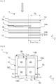
- figure 3 , 5 , 6 And 7 correspond to XZ sections in exploded views of three modes and an alternative embodiment of a photovoltaic module before the lamination step of the manufacturing method according to the invention.
- FIG. 4 corresponds to an XY top view of a particular embodiment of the first embodiment.
- FIG 8 corresponds to an XY top view of a particular embodiment of the third embodiment.
- the photovoltaic module may comprise one or more of the following features.
- the first layer 2, and the fourth layer 12 where appropriate, comprises at least one polymer material.
- the polymer material of the first layer 2 can be chosen from: polycarbonate (PC), polymethyl methacrylate (PMMA), polyethylene terephthalate (PET), polyamide ( PA), a fluorinated polymer, in particular polyvinyl fluoride (PVF) or polyvinylidene fluoride (PVDF), ethylene tetrafluoroethylene (ETFE), ethylene chlorotrifluoroethylene (ECTFE), polytetrafluoroethylene (PTFE), Polychlorotrifluoroethylene (PCTFE ) and/or fluorinated ethylene propylene (FEP).
- PC polycarbonate
- PMMA polymethyl methacrylate
- PET polyethylene terephthalate
- PA polyamide
- a fluorinated polymer in particular polyvinyl fluoride (PVF) or polyvinylidene fluoride (PVDF), ethylene tetrafluoroethylene (ETFE), ethylene chlorotrifluoroethylene (ECTFE), polytetraflu
- the first layer 2 (and the fourth layer 12 if applicable) has a thickness of less than 50 ⁇ m, and advantageously comprised between 5 ⁇ m and 25 ⁇ m.
- the encapsulating assembly 3 (and the fifth layer 13 if applicable) can be made from at least one polymer material chosen from: acid copolymers, ionomers, poly(ethylene-vinyl acetate) (EVA ), vinyl acetals, such as polyvinyl butyrals (PVB), polyurethanes, polyvinyl chlorides, polyethylenes, such as linear low density polyethylenes, elastomeric polyolefin copolymers, copolymers of ⁇ -olefins and ⁇ -, ⁇ - carboxylic to ethylenic acid esters, such as ethylene-methyl acrylate copolymers and ethylene-butyl acrylate copolymers, silicone elastomers and/or epoxy resins.
- polymer material chosen from: acid copolymers, ionomers, poly(ethylene-vinyl acetate) (EVA ), vinyl acetals, such as polyvinyl butyrals (PVB), polyure
- the encapsulating assembly 3 has a total thickness e3 which is less than or equal to 150 ⁇ m, and preferably between 20 and 100 ⁇ m, and even more preferably between 50 ⁇ m and 75 ⁇ m.
- the encapsulant assembly 3 can in particular be made from two layers of polymer material 3a (upper encapsulant layer) and 3b (lower encapsulant layer). he can these may be two layers of poly(ethylene-vinyl acetate) (EVA) or two layers of ionomer, between which the photovoltaic cells 4 are arranged. Each layer 3a, 3b may have a thickness e3a, e3b less than or equal to 75 ⁇ m, and preferably less than or equal to 50 ⁇ m. These layers 3a and 3b, although preferentially of identical nature, can have different optical properties.
- the photovoltaic cells 4 can be chosen from: homojunction or heterojunction photovoltaic cells based on monocrystalline (c-Si) and/or multi-crystalline (mc-Si) silicon, and/or photovoltaic cells of the IBC type, and/or photovoltaic cells comprising at least one material among amorphous silicon (a-Si), microcrystalline silicon ( ⁇ C-Si), cadmium telluride (CdTe), copper-indium selenide (CIS) and copper-indium/gallium diselenide (CIGS) or multi-junction cells (IIVV).
- Their thickness is between 1 and 300 ⁇ m, and in particular between 1 and 200 ⁇ m.
- the photovoltaic cells 4 can have a thickness e4 of between 1 and 300 ⁇ m, in particular between 1 and 250 ⁇ m, or even between 1 and 200 ⁇ m, and advantageously between 70 ⁇ m and 150 ⁇ m.
- the spacing between two neighboring photovoltaic cells, or even consecutive or adjacent can be greater than or equal to 0.5 mm, in particular between 1 and 30 mm, and preferably equal to 2 mm.
- the photovoltaic cells 4 can be interconnected by soldered tinned copper strips.
- the thickness of the photovoltaic cell interconnection ribbons is adapted to be compatible with the lamination process and the low thickness of the encapsulating assembly.
- the cell interconnection ribbons can have a thickness of less than 100 ⁇ m and a width of less than 3 mm.
- the second layer 5 comprises a composite material of the preimpregnated type based on polymer resin and fibers having a surface weight of less than 150 g/m 2 , and advantageously between 50 g/m 2 and 115 g/m 2 . It may for example consist of said at least one composite material.
- the fabric weft of the prepreg may have a basis weight less than or equal to 50 g/m 2 , and the polymer resin impregnation rate may be between 30 and 70% by mass.
- the composite material of the second layer 5 can be a prepreg based on polymer resin and fibers, the polymer being chosen from polyester, epoxy and/or acrylic, and the fibers being chosen from glass fibers, carbon and/or aramid.
- the second layer 5 may in particular have a thickness e5 less than or equal to 100 ⁇ m, in particular between 50 ⁇ m and 80 ⁇ m.
- the third layer 15 (or reinforcement layer) is also made of a composite material of the preimpregnated type based on polymer resin and fibers. This can be one of the materials listed above, with reference to the second layer 5.
- the third layer 15 is the same material as the second layer 5.
- the third layer 15 may in particular have a basis weight of between 50 g/m 2 and 150 g/m 2.
- the third layer may in particular have a thickness e15 of less than or equal to 100 ⁇ m, in particular of between 50 ⁇ m and 80 ⁇ m.
- first layer and/or the second layer of the photovoltaic module can be formed in one or more parts, namely that they can be monolayer or multilayer.
- the first layer 2 and the second layer 5 define the edges of the photovoltaic module 1, and also the encapsulating assembly which extends to the edges of the module.
- the plurality of photovoltaic cells 4 is separated by a distance D A from an edge 1A of the photovoltaic module 1.
- the photovoltaic module 1 also comprises a third layer 15, or reinforcement layer, located below the plurality of photovoltaic cells 4 and above the lower encapsulant layer 3b.
- This third layer forms a peripheral band 15A which extends from edge 1A and overflows below the photovoltaic cell 41 (or photovoltaic cells) closest (the closest) to edge 1A.
- the width L 15A of this peripheral band is thus greater than the distance D A .
- the distance D A can be equal to 50 mm and the width L 15A of the peripheral strip 15A equal to 70 mm. More generally, the difference between the width L 15A and the distance D A is less than or equal to 30 mm, preferably less than or equal to 20 mm, and even more preferably between 10 and 20 mm.
- FIG. 4 is a top view of an exemplary embodiment of the embodiment of the picture 3 .
- the photovoltaic cells are distant from all the edges 1A, 1B, 1C, 1D of the photovoltaic module 1 by a distance D A , D B , D C , D D .
- Four photovoltaic cells 41, 42, 43, 44 are represented but this number is not limiting, and there could be more, or less.
- the third layer 15 forms four peripheral bands 15A, 15B, 15C, 15D, one per edge 1A, 1B, 1C, 1D, thus forming a frame.
- Each peripheral band extending from an edge and overflows below the two photovoltaic cells closest to the edge.
- the width L 15A (resp L 15B , L 15C , L 15D ) of each illustrated peripheral strip is greater than the distance D A (resp D B , D C , D D ) between the edge parallel to said strip and the plurality of cells photovoltaic (4).
- the distances D A , D B , D C , D D can be equal to 50 mm and the widths L 15A , L 15B , L 15C , L 15D of the peripheral bands 15A, 15B, 15C, 15D equal at 70mm.
- the difference between the width L 15A (resp L 15B , L 15C , L 15D ) of strip of the third layer 15 and the distance D A (resp D B , D C , D D ) between the edge parallel to said strip and the cells is less than or equal to 30 mm, preferably less than or equal to 20 mm, and even more preferably between 10 and 20 mm.
- each peripheral strip has the shape of an isosceles trapezium with an angle of 45°.
- the frame may be integral.
- FIG. 5 illustrates, in section and in exploded view, a variant embodiment of the first embodiment.
- the photovoltaic module 1 may include all or part of the characteristics described above, and in particular those related to the figures 3 to 4 which will therefore not be described again.
- the photovoltaic module 1 comprises a fourth layer 12 forming the rear face of the photovoltaic module 1, the second layer 5 being located between the fourth layer 12 and the encapsulating assembly 3.
- This fourth layer 12 is constituted by the same material as that constituting the first layer 2 forming the front face of the photovoltaic module 1.
- this material corresponds to ethylene chlorotrifluoroethylene (ECTFE), also known under the name Halar ® .
- the fourth layer 12 has a lower thickness e12, or equal in this variant of the figure 5 , to the thickness e2 of the first layer 2.
- the fourth layer 12 advantageously makes it possible to achieve dielectric and chemical insulation of the module 1.
- the fourth layer 12 forming the rear face is also represented on the figure 6 And 7 . However, it could be omitted.
- FIG. 6 illustrates, in section and in exploded view, a second embodiment of a photovoltaic module.
- This photovoltaic module of the figure 6 may include all or part of the characteristics described above, and in particular those related to the figures 3 to 5 which will therefore not be described again.
- the upper encapsulant layer (3a) is separated by a distance D 3 from the edge 1A of the photovoltaic module. This distance D 3 is less than the distance D A so that the upper encapsulant layer (3a) can still protect the photovoltaic cells.
- the upper encapsulant layer (3a) may be distant from all the edges of the photovoltaic module, and in particular may be distant by the same distance D 3 from all the edges of the photovoltaic module, as for example in a configuration of the type of figure 4 And 8 .
- the distance D A can be equal to 50 mm, the width L 15A of the peripheral strip 15A equal to 70 mm and the distance D 3 equal to 30 mm.
- the difference between the width L 15A (resp L 15B , L 15C , L 15D ) and the distance D A (resp D B , D C , D D ) is less than or equal to 30 mm, preferably less than or equal to 20 mm, and even more preferably between 10 and 20 mm, and the difference between D A (resp D B , D C , D D ) and D 3 is less than or equal to 10 mm.
- FIG. 7 illustrates, in section and in exploded view, a third embodiment of a photovoltaic module.
- This photovoltaic module of the figure 7 may include all or part of the characteristics described above, and in particular those related to the figures 3 to 5 which will therefore not be described again.
- the photovoltaic module comprises a fifth layer 13 located below the second layer 5 and above the fourth layer 12.
- This fifth layer forms at least one peripheral strip 13A extending from an edge 1A and overflows below the photovoltaic cell 41 (or photovoltaic cells) closest (the closest) to the edge 1A.
- the width L 13A of this peripheral strip is greater than the distance D A .
- This fifth layer 13 is preferably made of the same material as the encapsulating assembly 3.
- the fifth layer is made of a material different from the material of the encapsulating assembly but it must have at least the same thermomechanical properties.
- the advantage of this fifth layer is to symmetrize the edge and/or the edges.
- the distance D A can be equal to 50 mm, the width L 15A of the peripheral strip 15A equal to 70 mm and the width L 13A of the peripheral strip 13A equal to 70 mm.
- the difference between the width L 13A and the distance D A is less than or equal to 30 mm, preferably less than or equal to 20 mm and even more preferably between 10 and 20 mm.
- the width L 13A is equal to the width L 15A .
- FIG 8 corresponds to a bottom view of a particular embodiment of the third embodiment, in which only the fourth layer 12 (from below), the fifth layer 13 and four photovoltaic cells 41, 42, 43 have been shown, 44 (the layers 5, 3b, 15 which are between the layer 13 and the cells are not represented, although present, to make the figure more readable, likewise for the layers above the cells).
- the photovoltaic cells are distant from all the edges 1A, 1B, 1C, 1D of the photovoltaic module 1 by a distance D A , D B , D C , D D .
- Four cells are represented but this number is not limiting, and there could be more, or less.
- the fifth layer 13 can thus form four peripheral bands, one per edge, as for example represented in the configuration of the figure 8 , thus also forming a frame.
- the frame may be in one piece.
- the distances D A , D B , D C , D D can be equal to 50 mm, and the widths L 13A , L 13B , L 13C , L 13D of the peripheral bands 13A, 13B, 13C, 13D equal to 70 mm.
- the difference between the bandwidth L 13A (resp L 13B , L 13C , L 13D ) of the fifth layer and the distance D A (resp D B , D C , D D ) is less than or equal to 30 mm, preferably less than or equal to 20 mm and even more preferably between 10 and 20 mm.
- the width L 13A , (resp L 13B , L 13C , L 13D ) of the band of the fifth layer 13 is equal to the width L 15A , (resp L 15B , L 15C , L 15D ) of the band of the third layer 15.
- the fifth layer 13 is preferably of the same geometric shape as the third layer 15, so that they can overlap.
- the fifth layer 13 may in particular have a thickness e13 less than or equal to 150 ⁇ m, or even less than or equal to 100 ⁇ m.
- the production of a photovoltaic module 1 is carried out in a single hot lamination step, at a temperature of between 130° C. and 170° C., and in particular of the order of 150° C., and for a duration of the cycle of lamination of at least 10 minutes, and in particular between 10 and 20 minutes, of the constituent layers forming the photovoltaic module 1.
Claims (18)
- Photovoltaikmodul (1), das Folgendes aufweist:- eine transparente erste Schicht (2), die die Vorderseite des Photovoltaikmoduls (1) bildet, die dazu bestimmt ist, einen Lichtstrom zu empfangen,- eine Vielzahl von photovoltaischen Zellen (4), die Seite an Seite angeordnet und elektrisch miteinander verbunden sind,- eine Einkapselungsanordnung (3), die die Vielzahl von photovoltaischen Zellen (4) einkapseln kann und einen unteren Teil (3b) und einen oberen Teil (3a) aufweist, wobei die Einkapselungsanordnung vorzugsweise aus Polymer besteht,- eine zweite Schicht (5), die mindestens ein Verbundmaterial auf Polymerharz- und Faserbasis umfasst,wobei sich die Einkapselungsanordnung (3) und die Vielzahl von photovoltaischen Zellen (4) zwischen der ersten (2) und der zweiten (5) Schicht befinden,wobei mindestens die erste Schicht (2) und die zweite Schicht (5) die Ränder (1A, 1B, 1C, 1D) des Photovoltaikmoduls (1) definieren;dadurch gekennzeichnet, dass die Vielzahl von photovoltaischen Zellen (4) in einer Distanz DA von ungleich Null von mindestens einem Rand (1A) des Photovoltaikmoduls (1) beabstandet ist, und dadurch, dass das Photovoltaikmodul (1) ferner eine dritte Schicht (15) oder Verstärkungsschicht umfasst, die sich unter der Vielzahl von photovoltaischen Zellen (4) und über dem unteren Teil (3b) der Einkapselungsanordnung (3) befindet, wobei die dritte Schicht mindestens einen peripheren Streifen (15A) bildet, der sich von dem mindestens einen Rand (1A) zur Mitte des Moduls hin erstreckt und dessen Breite (L15A) gleich der oder größer als die Distanz DA ist; wobei die dritte Schicht mindestens ein Verbundmaterial auf Polymerharz- und Faserbasis umfasst.
- Photovoltaikmodul (1) nach Anspruch 1, wobei die Differenz zwischen der Breite (L15A) des mindestens einen peripheren Streifens (15A) und der Distanz DA zwischen der Vielzahl von photovoltaischen Zellen (4) und dem mindestens einen Rand (1A) kleiner als oder gleich 30 mm, vorzugsweise kleiner als oder gleich 20 mm ist.
- Photovoltaikmodul (1) nach Anspruch 1 oder Anspruch 2, wobei die dritte Schicht (15) und/oder die zweite Schicht (5) aus einem Verbundmaterial auf Polymerharz- und Faserbasis besteht,- wobei das Polymer vorzugsweise aus Polyester, Epoxy und/oder Acryl ausgewählt ist; und/oder- wobei die Fasern vorzugsweise aus Glas-, Kohlenstoff- und/oder Aramidfasern ausgewählt sind.
- Photovoltaikmodul (1) nach einem der Ansprüche 1 bis 3, wobei die dritte Schicht (15) aus demselben Verbundmaterial wie die zweite Schicht (5) besteht.
- Photovoltaikmodul (1) nach einem der Ansprüche 1 bis 4, wobei die dritte Schicht (15) mehrere periphere Streifen (15A, 15B, 15C, 15D), vorzugsweise mindestens zwei gegenüberliegende Streifen und noch bevorzugter vier Streifen bildet, wobei sich jeder periphere Streifen von einem Rand (1A, 1B, 1C, 1D) des Photovoltaikmoduls (1) zur Mitte des Moduls erstreckt, wobei die Breite (L15A, L15B, L15C, L15D) jedes peripheren Streifens gleich der oder größer als die Distanz DA, DB, DC, DD zwischen dem Rand und der Vielzahl von photovoltaischen Zellen (4) ist, wobei die Differenz zwischen der Breite jedes peripheren Streifens und der Distanz DA, DB, DC, DD vorzugsweise kleiner als oder gleich 30 mm und noch bevorzugter kleiner als oder gleich 20 mm ist.
- Photovoltaikmodul (1) nach einem der Ansprüche 1 bis 5, wobei sich die Einkapselungsanordnung (3) bis zu den Rändern (1A, IB, 1C, 1D) des Photovoltaikmoduls (1) erstreckt.
- Photovoltaikmodul (1) nach einem der Ansprüche 1 bis 5, wobei der obere Teil (3a) der Einkapselungsanordnung (3) um eine Distanz D3A von dem mindestens einen Rand (1A) des Photovoltaikmoduls (1) beabstandet ist, wobei die Distanz D3A ungleich Null und kleiner als die Distanz DA zwischen dem mindestens einen Rand und der Vielzahl von photovoltaischen Zellen ist, wobei der Abstand zwischen den Distanzen DA und D3A vorzugsweise kleiner als oder gleich 10 mm ist.
- Photovoltaikmodul (1) nach einem der vorhergehenden Ansprüche, das ferner eine fünfte Schicht (13), die vorzugsweise aus Polymer besteht, umfasst, die unter der zweiten Schicht (5) angeordnet ist, wobei die fünfte Schicht mindestens einen peripheren Streifen (13A) bildet, der sich von dem mindestens einen Rand (1A) zur Mitte des Moduls hin erstreckt und dessen Breite (L13A) gleich der oder größer als die Distanz DA zwischen dem mindestens einen Rand und der Vielzahl von photovoltaischen Zellen ist, wobei die Differenz zwischen der Breite und der Distanz vorzugsweise kleiner als oder gleich 30 mm und noch bevorzugter kleiner als oder gleich 20 mm ist.
- Photovoltaikmodul (1) nach Anspruch 8, wobei die fünfte Schicht (13) mehrere periphere Streifen (13A, 13B, 13C, 13D), vorzugsweise mindestens zwei gegenüberliegende Streifen und noch bevorzugter vier Streifen bildet, wobei sich jeder periphere Streifen von einem Rand (1A, 1B, 1C, 1D) des Photovoltaikmoduls (1) zur Mitte des Moduls erstreckt und die Breite (L13A, L13B, L13C, L13D) jedes peripheren Streifens gleich der oder größer als die Distanz DA, DB, DC, DD zwischen dem Rand und der Vielzahl von photovoltaischen Zellen (4) ist, wobei die Differenz zwischen der Breite und der Distanz vorzugsweise kleiner als oder gleich 30 mm und noch bevorzugter kleiner als oder gleich 20 mm ist.
- Photovoltaikmodul (1) nach einem der Ansprüche 8 oder 9, wobei die fünfte Schicht (13) aus einem Material mit den gleichen thermomechanischen Eigenschaften wie das Material der Einkapselungsanordnung, vorzugsweise aus dem gleichen Material wie die Einkapselungsanordnung (3) besteht.
- Photovoltaikmodul (1) nach einem der Ansprüche 8 bis 10, wobei die Abmessungen der fünften Schicht (13) im Wesentlichen gleich den Abmessungen der dritten Schicht (15) sind.
- Photovoltaikmodul (1) nach einem der vorhergehenden Ansprüche, das ferner Folgendes umfasst:- eine vierte Schicht (12), die die Rückseite des Photovoltaikmoduls (1) bildet, wobei sich die zweite Schicht (5) zwischen der Einkapselungsanordnung (3) und der vierten Schicht (12) befindet, wobei die vierte Schicht aus demselben Material wie das der ersten Schicht (2) besteht und eine Dicke aufweist, die gleich der oder kleiner als die erste(n) Schicht (2) ist.
- Photovoltaikmodul (1) nach einem der vorhergehenden Ansprüche, wobei die erste Schicht (2) aus einem polymeren Material besteht.
- Photovoltaikmodul (1) nach einem der vorhergehenden Ansprüche, wobei die erste Schicht (2) eine Dicke (e2) kleiner als oder gleich 50 µm aufweist.
- Photovoltaikmodul (1) nach einem der vorhergehenden Ansprüche, wobei die Einkapselungsanordnung (3) eine maximale Dicke (e3) von weniger als 150 µm aufweist.
- Photovoltaikmodul (1) nach einem der vorhergehenden Ansprüche, wobei die zweite Schicht (5) ein Flächengewicht von weniger als 150 g/m2 aufweist.
- Photovoltaikmodul (1) nach einem der vorhergehenden Ansprüche, wobei die Einkapselungsanordnung (3) eine zwischen der ersten Schicht (2) und der Vielzahl von photovoltaischen Zellen (4) angeordnete obere Einkapselungsschicht (3a) und eine zwischen der Vielzahl von photovoltaischen Zellen (4) und der zweiten Schicht (5) angeordnete untere Einkapselungsschicht (3b) umfasst.
- Verfahren zur Herstellung eines Photovoltaikmodul (1), ausgewählt nach einem der Ansprüche 1 bis 17, dadurch gekennzeichnet, dass es einen Heißlaminierungsschritt bei einer Temperatur zwischen 130°C und 170°C, insbesondere in der Größenordnung von 150°C, und während einer Dauer des Laminierzyklus von mindestens 10 Minuten, insbesondere zwischen 10 und 20 Minuten, der das Photovoltaikmodul (1) bildenden Schichten aufweist.
Applications Claiming Priority (1)
| Application Number | Priority Date | Filing Date | Title |
|---|---|---|---|
| FR2012016A FR3116650B1 (fr) | 2020-11-23 | 2020-11-23 | Module photovoltaïque léger et flexible amélioré |
Publications (3)
| Publication Number | Publication Date |
|---|---|
| EP4002491A1 EP4002491A1 (de) | 2022-05-25 |
| EP4002491B1 true EP4002491B1 (de) | 2023-07-19 |
| EP4002491C0 EP4002491C0 (de) | 2023-07-19 |
Family
ID=74860041
Family Applications (1)
| Application Number | Title | Priority Date | Filing Date |
|---|---|---|---|
| EP21208798.5A Active EP4002491B1 (de) | 2020-11-23 | 2021-11-17 | Verbessertes leichtes und flexibles fotovoltaikmodul |
Country Status (6)
| Country | Link |
|---|---|
| US (1) | US11784268B2 (de) |
| EP (1) | EP4002491B1 (de) |
| JP (1) | JP2022082511A (de) |
| CN (1) | CN114530513A (de) |
| ES (1) | ES2955549T3 (de) |
| FR (1) | FR3116650B1 (de) |
Families Citing this family (2)
| Publication number | Priority date | Publication date | Assignee | Title |
|---|---|---|---|---|
| FR3134653A1 (fr) * | 2022-04-15 | 2023-10-20 | Commissariat A L'energie Atomique Et Aux Energies Alternatives | Module photovoltaïque léger comportant un cadre composite intégré |
| TWI818690B (zh) * | 2022-08-23 | 2023-10-11 | 友達光電股份有限公司 | 太陽能模組 |
Family Cites Families (8)
| Publication number | Priority date | Publication date | Assignee | Title |
|---|---|---|---|---|
| JP2002141542A (ja) * | 2000-10-31 | 2002-05-17 | Canon Inc | 太陽電池モジュール、並びに、その製造方法およびその固定方法 |
| JP2011187657A (ja) * | 2010-03-08 | 2011-09-22 | Fuji Electric Co Ltd | 太陽電池モジュール及び太陽電池モジュールの補強方法 |
| CN203367314U (zh) * | 2013-05-22 | 2013-12-25 | 马广胜 | 加固的太阳能电池模块 |
| SI2863443T1 (sl) * | 2013-10-17 | 2016-09-30 | Das Energy Gmbh | Fotovoltaični panel in postopek njegove izdelave |
| US9004410B1 (en) * | 2014-10-24 | 2015-04-14 | Alliance Spacesystems, Llc | Deployable boom for collecting electromagnetic energy |
| CN110073501A (zh) * | 2016-12-15 | 2019-07-30 | 松下知识产权经营株式会社 | 太阳能电池模块 |
| RU178429U1 (ru) * | 2017-08-21 | 2018-04-04 | Акционерное Общество "ТЕЛЕКОМ-СТВ" | Фотоэлектрический усиленный гибкий модуль |
| FR3081615B1 (fr) | 2018-05-22 | 2021-09-17 | Commissariat Energie Atomique | Module photovoltaique leger et flexible comportant une couche avant en polymere et une couche arriere en materiau composite |
-
2020
- 2020-11-23 FR FR2012016A patent/FR3116650B1/fr active Active
-
2021
- 2021-11-17 JP JP2021186850A patent/JP2022082511A/ja active Pending
- 2021-11-17 EP EP21208798.5A patent/EP4002491B1/de active Active
- 2021-11-17 ES ES21208798T patent/ES2955549T3/es active Active
- 2021-11-19 US US17/531,548 patent/US11784268B2/en active Active
- 2021-11-23 CN CN202111391644.4A patent/CN114530513A/zh active Pending
Also Published As
| Publication number | Publication date |
|---|---|
| US11784268B2 (en) | 2023-10-10 |
| ES2955549T3 (es) | 2023-12-04 |
| FR3116650B1 (fr) | 2022-11-25 |
| EP4002491C0 (de) | 2023-07-19 |
| EP4002491A1 (de) | 2022-05-25 |
| US20220165898A1 (en) | 2022-05-26 |
| CN114530513A (zh) | 2022-05-24 |
| JP2022082511A (ja) | 2022-06-02 |
| FR3116650A1 (fr) | 2022-05-27 |
Similar Documents
| Publication | Publication Date | Title |
|---|---|---|
| EP3776668B1 (de) | Leichtgewichtiges und flexibles photovoltaisches modul mit einer vorderen schicht aus einem polymer und einer hinteren schicht aus einem verbundwerkstoff | |
| EP4002491B1 (de) | Verbessertes leichtes und flexibles fotovoltaikmodul | |
| EP3493277B1 (de) | Verfahren zur verbindung von photovoltaikzellen mit einer elektrode, ausgestattet mit metallnanodrähten | |
| EP3859793B1 (de) | Leichtes fotovoltaikmodul mit einer vorderen und einer hinteren schicht aus verbundmaterialien | |
| WO2011004329A1 (fr) | Procédé de fabrication de cellules photovoltaiques multi-jonctions et multi-électrodes | |
| WO2017085017A1 (fr) | Module photovoltaïque léger comportant une couche avant en verre ou polymère et une couche arrière alvéolaire | |
| EP3378102B1 (de) | Leichtes fotovoltaikmodul mit einer vorderschicht aus glas oder polymer und einer hinterschicht mit erhöhten abschnitten | |
| FR3107990A1 (fr) | Module photovoltaïque léger comportant des couches avant et arrière polymère et des renforts fibrés | |
| FR3081614A1 (fr) | Module photovoltaique comportant une ou plusieurs diodes de bypass en face arriere d'une cellule photovoltaique du module | |
| EP3496160A1 (de) | Fotovoltaikmodul, das fotovoltaikzellen umfasst, die mithilfe von verbindungselementen miteinander verbunden sind | |
| EP3657551B1 (de) | Photovoltaikvorrichtung mit mindestens einer schicht auf mindestens einem photovoltaikmodul mit verschleissanzeige | |
| EP4032131B1 (de) | Fotovoltaikmodul mit einem elektrisch leitenden verbindungselement | |
| EP3657552B1 (de) | Fotovoltaische vorrichtung, die mindestens eine schleifbare beschichtungsschicht auf mindestens einem fotovoltaischen modul umfasst | |
| EP3321975B1 (de) | Fotovoltaikmodul, das eine haftschicht zwischen einer schutzschicht und einer einkapselungseinheit umfasst | |
| FR3116651A1 (fr) | Procédé de fabrication d’un module photovoltaïque léger et flexible intégrant une protection thermique | |
| WO2023041864A1 (fr) | Module photovoltaïque léger comportant une couche avant en verre et polymère | |
| WO2023203289A1 (fr) | Module photovoltaïque léger et résistant aux chocs | |
| EP4310924A1 (de) | Leichtes photovoltaikmodul mit verbundverstärkungsrahmen | |
| WO2023199005A1 (fr) | Module photovoltaïque léger comportant un cadre composite intégré | |
| FR3071682A1 (fr) | Procede de fabrication d'un module photovoltaique avec controle de la distance inter-series de cellules photovoltaiques |
Legal Events
| Date | Code | Title | Description |
|---|---|---|---|
| PUAI | Public reference made under article 153(3) epc to a published international application that has entered the european phase |
Free format text: ORIGINAL CODE: 0009012 |
|
| STAA | Information on the status of an ep patent application or granted ep patent |
Free format text: STATUS: REQUEST FOR EXAMINATION WAS MADE |
|
| 17P | Request for examination filed |
Effective date: 20211117 |
|
| AK | Designated contracting states |
Kind code of ref document: A1 Designated state(s): AL AT BE BG CH CY CZ DE DK EE ES FI FR GB GR HR HU IE IS IT LI LT LU LV MC MK MT NL NO PL PT RO RS SE SI SK SM TR |
|
| GRAP | Despatch of communication of intention to grant a patent |
Free format text: ORIGINAL CODE: EPIDOSNIGR1 |
|
| STAA | Information on the status of an ep patent application or granted ep patent |
Free format text: STATUS: GRANT OF PATENT IS INTENDED |
|
| INTG | Intention to grant announced |
Effective date: 20230221 |
|
| GRAS | Grant fee paid |
Free format text: ORIGINAL CODE: EPIDOSNIGR3 |
|
| GRAA | (expected) grant |
Free format text: ORIGINAL CODE: 0009210 |
|
| STAA | Information on the status of an ep patent application or granted ep patent |
Free format text: STATUS: THE PATENT HAS BEEN GRANTED |
|
| AK | Designated contracting states |
Kind code of ref document: B1 Designated state(s): AL AT BE BG CH CY CZ DE DK EE ES FI FR GB GR HR HU IE IS IT LI LT LU LV MC MK MT NL NO PL PT RO RS SE SI SK SM TR |
|
| REG | Reference to a national code |
Ref country code: GB Ref legal event code: FG4D Free format text: NOT ENGLISH |
|
| REG | Reference to a national code |
Ref country code: CH Ref legal event code: EP |
|
| REG | Reference to a national code |
Ref country code: DE Ref legal event code: R096 Ref document number: 602021003604 Country of ref document: DE |
|
| REG | Reference to a national code |
Ref country code: IE Ref legal event code: FG4D Free format text: LANGUAGE OF EP DOCUMENT: FRENCH |
|
| U01 | Request for unitary effect filed |
Effective date: 20230727 |
|
| U07 | Unitary effect registered |
Designated state(s): AT BE BG DE DK EE FI FR IT LT LU LV MT NL PT SE SI Effective date: 20230802 |
|
| REG | Reference to a national code |
Ref country code: LT Ref legal event code: MG9D |
|
| U20 | Renewal fee paid [unitary effect] |
Year of fee payment: 3 Effective date: 20231020 |
|
| REG | Reference to a national code |
Ref country code: ES Ref legal event code: FG2A Ref document number: 2955549 Country of ref document: ES Kind code of ref document: T3 Effective date: 20231204 |
|
| PG25 | Lapsed in a contracting state [announced via postgrant information from national office to epo] |
Ref country code: GR Free format text: LAPSE BECAUSE OF FAILURE TO SUBMIT A TRANSLATION OF THE DESCRIPTION OR TO PAY THE FEE WITHIN THE PRESCRIBED TIME-LIMIT Effective date: 20231020 |
|
| PGFP | Annual fee paid to national office [announced via postgrant information from national office to epo] |
Ref country code: ES Payment date: 20231207 Year of fee payment: 3 |
|
| PG25 | Lapsed in a contracting state [announced via postgrant information from national office to epo] |
Ref country code: IS Free format text: LAPSE BECAUSE OF FAILURE TO SUBMIT A TRANSLATION OF THE DESCRIPTION OR TO PAY THE FEE WITHIN THE PRESCRIBED TIME-LIMIT Effective date: 20231119 |
|
| PG25 | Lapsed in a contracting state [announced via postgrant information from national office to epo] |
Ref country code: RS Free format text: LAPSE BECAUSE OF FAILURE TO SUBMIT A TRANSLATION OF THE DESCRIPTION OR TO PAY THE FEE WITHIN THE PRESCRIBED TIME-LIMIT Effective date: 20230719 Ref country code: NO Free format text: LAPSE BECAUSE OF FAILURE TO SUBMIT A TRANSLATION OF THE DESCRIPTION OR TO PAY THE FEE WITHIN THE PRESCRIBED TIME-LIMIT Effective date: 20231019 Ref country code: IS Free format text: LAPSE BECAUSE OF FAILURE TO SUBMIT A TRANSLATION OF THE DESCRIPTION OR TO PAY THE FEE WITHIN THE PRESCRIBED TIME-LIMIT Effective date: 20231119 Ref country code: HR Free format text: LAPSE BECAUSE OF FAILURE TO SUBMIT A TRANSLATION OF THE DESCRIPTION OR TO PAY THE FEE WITHIN THE PRESCRIBED TIME-LIMIT Effective date: 20230719 Ref country code: GR Free format text: LAPSE BECAUSE OF FAILURE TO SUBMIT A TRANSLATION OF THE DESCRIPTION OR TO PAY THE FEE WITHIN THE PRESCRIBED TIME-LIMIT Effective date: 20231020 |
|
| PG25 | Lapsed in a contracting state [announced via postgrant information from national office to epo] |
Ref country code: PL Free format text: LAPSE BECAUSE OF FAILURE TO SUBMIT A TRANSLATION OF THE DESCRIPTION OR TO PAY THE FEE WITHIN THE PRESCRIBED TIME-LIMIT Effective date: 20230719 |