EP3985716A1 - Semiconductor device - Google Patents
Semiconductor device Download PDFInfo
- Publication number
- EP3985716A1 EP3985716A1 EP20823491.4A EP20823491A EP3985716A1 EP 3985716 A1 EP3985716 A1 EP 3985716A1 EP 20823491 A EP20823491 A EP 20823491A EP 3985716 A1 EP3985716 A1 EP 3985716A1
- Authority
- EP
- European Patent Office
- Prior art keywords
- cell
- bonding pad
- current
- wiring layer
- current detection
- Prior art date
- Legal status (The legal status is an assumption and is not a legal conclusion. Google has not performed a legal analysis and makes no representation as to the accuracy of the status listed.)
- Pending
Links
Images




Classifications
-
- H—ELECTRICITY
- H10—SEMICONDUCTOR DEVICES; ELECTRIC SOLID-STATE DEVICES NOT OTHERWISE PROVIDED FOR
- H10D—INORGANIC ELECTRIC SEMICONDUCTOR DEVICES
- H10D64/00—Electrodes of devices having potential barriers
- H10D64/20—Electrodes characterised by their shapes, relative sizes or dispositions
- H10D64/27—Electrodes not carrying the current to be rectified, amplified, oscillated or switched, e.g. gates
- H10D64/311—Gate electrodes for field-effect devices
- H10D64/411—Gate electrodes for field-effect devices for FETs
- H10D64/511—Gate electrodes for field-effect devices for FETs for IGFETs
- H10D64/517—Gate electrodes for field-effect devices for FETs for IGFETs characterised by the conducting layers
- H10D64/518—Gate electrodes for field-effect devices for FETs for IGFETs characterised by the conducting layers characterised by their lengths or sectional shapes
-
- H—ELECTRICITY
- H10—SEMICONDUCTOR DEVICES; ELECTRIC SOLID-STATE DEVICES NOT OTHERWISE PROVIDED FOR
- H10D—INORGANIC ELECTRIC SEMICONDUCTOR DEVICES
- H10D30/00—Field-effect transistors [FET]
- H10D30/60—Insulated-gate field-effect transistors [IGFET]
- H10D30/64—Double-diffused metal-oxide semiconductor [DMOS] FETs
- H10D30/66—Vertical DMOS [VDMOS] FETs
- H10D30/669—Vertical DMOS [VDMOS] FETs having voltage-sensing or current-sensing structures, e.g. emulator sections or overcurrent sensing cells
-
- H—ELECTRICITY
- H10—SEMICONDUCTOR DEVICES; ELECTRIC SOLID-STATE DEVICES NOT OTHERWISE PROVIDED FOR
- H10D—INORGANIC ELECTRIC SEMICONDUCTOR DEVICES
- H10D62/00—Semiconductor bodies, or regions thereof, of devices having potential barriers
- H10D62/10—Shapes, relative sizes or dispositions of the regions of the semiconductor bodies; Shapes of the semiconductor bodies
- H10D62/124—Shapes, relative sizes or dispositions of the regions of semiconductor bodies or of junctions between the regions
- H10D62/126—Top-view geometrical layouts of the regions or the junctions
- H10D62/127—Top-view geometrical layouts of the regions or the junctions of cellular field-effect devices, e.g. multicellular DMOS transistors or IGBTs
-
- H—ELECTRICITY
- H10—SEMICONDUCTOR DEVICES; ELECTRIC SOLID-STATE DEVICES NOT OTHERWISE PROVIDED FOR
- H10D—INORGANIC ELECTRIC SEMICONDUCTOR DEVICES
- H10D64/00—Electrodes of devices having potential barriers
- H10D64/20—Electrodes characterised by their shapes, relative sizes or dispositions
- H10D64/27—Electrodes not carrying the current to be rectified, amplified, oscillated or switched, e.g. gates
- H10D64/311—Gate electrodes for field-effect devices
- H10D64/411—Gate electrodes for field-effect devices for FETs
- H10D64/511—Gate electrodes for field-effect devices for FETs for IGFETs
- H10D64/512—Disposition of the gate electrodes, e.g. buried gates
-
- H—ELECTRICITY
- H10—SEMICONDUCTOR DEVICES; ELECTRIC SOLID-STATE DEVICES NOT OTHERWISE PROVIDED FOR
- H10D—INORGANIC ELECTRIC SEMICONDUCTOR DEVICES
- H10D84/00—Integrated devices formed in or on semiconductor substrates that comprise only semiconducting layers, e.g. on Si wafers or on GaAs-on-Si wafers
- H10D84/01—Manufacture or treatment
- H10D84/0123—Integrating together multiple components covered by H10D12/00 or H10D30/00, e.g. integrating multiple IGBTs
- H10D84/0126—Integrating together multiple components covered by H10D12/00 or H10D30/00, e.g. integrating multiple IGBTs the components including insulated gates, e.g. IGFETs
- H10D84/0149—Manufacturing their interconnections or electrodes, e.g. source or drain electrodes
-
- H—ELECTRICITY
- H10—SEMICONDUCTOR DEVICES; ELECTRIC SOLID-STATE DEVICES NOT OTHERWISE PROVIDED FOR
- H10D—INORGANIC ELECTRIC SEMICONDUCTOR DEVICES
- H10D84/00—Integrated devices formed in or on semiconductor substrates that comprise only semiconducting layers, e.g. on Si wafers or on GaAs-on-Si wafers
- H10D84/01—Manufacture or treatment
- H10D84/02—Manufacture or treatment characterised by using material-based technologies
- H10D84/03—Manufacture or treatment characterised by using material-based technologies using Group IV technology, e.g. silicon technology or silicon-carbide [SiC] technology
- H10D84/038—Manufacture or treatment characterised by using material-based technologies using Group IV technology, e.g. silicon technology or silicon-carbide [SiC] technology using silicon technology, e.g. SiGe
-
- H—ELECTRICITY
- H10—SEMICONDUCTOR DEVICES; ELECTRIC SOLID-STATE DEVICES NOT OTHERWISE PROVIDED FOR
- H10D—INORGANIC ELECTRIC SEMICONDUCTOR DEVICES
- H10D84/00—Integrated devices formed in or on semiconductor substrates that comprise only semiconducting layers, e.g. on Si wafers or on GaAs-on-Si wafers
- H10D84/80—Integrated devices formed in or on semiconductor substrates that comprise only semiconducting layers, e.g. on Si wafers or on GaAs-on-Si wafers characterised by the integration of at least one component covered by groups H10D12/00 or H10D30/00, e.g. integration of IGFETs
- H10D84/82—Integrated devices formed in or on semiconductor substrates that comprise only semiconducting layers, e.g. on Si wafers or on GaAs-on-Si wafers characterised by the integration of at least one component covered by groups H10D12/00 or H10D30/00, e.g. integration of IGFETs of only field-effect components
- H10D84/83—Integrated devices formed in or on semiconductor substrates that comprise only semiconducting layers, e.g. on Si wafers or on GaAs-on-Si wafers characterised by the integration of at least one component covered by groups H10D12/00 or H10D30/00, e.g. integration of IGFETs of only field-effect components of only insulated-gate FETs [IGFET]
- H10D84/83125—Integrated devices formed in or on semiconductor substrates that comprise only semiconducting layers, e.g. on Si wafers or on GaAs-on-Si wafers characterised by the integration of at least one component covered by groups H10D12/00 or H10D30/00, e.g. integration of IGFETs of only field-effect components of only insulated-gate FETs [IGFET] the IGFETs characterised by having shared source or drain regions
-
- H—ELECTRICITY
- H10—SEMICONDUCTOR DEVICES; ELECTRIC SOLID-STATE DEVICES NOT OTHERWISE PROVIDED FOR
- H10D—INORGANIC ELECTRIC SEMICONDUCTOR DEVICES
- H10D84/00—Integrated devices formed in or on semiconductor substrates that comprise only semiconducting layers, e.g. on Si wafers or on GaAs-on-Si wafers
- H10D84/80—Integrated devices formed in or on semiconductor substrates that comprise only semiconducting layers, e.g. on Si wafers or on GaAs-on-Si wafers characterised by the integration of at least one component covered by groups H10D12/00 or H10D30/00, e.g. integration of IGFETs
- H10D84/82—Integrated devices formed in or on semiconductor substrates that comprise only semiconducting layers, e.g. on Si wafers or on GaAs-on-Si wafers characterised by the integration of at least one component covered by groups H10D12/00 or H10D30/00, e.g. integration of IGFETs of only field-effect components
- H10D84/83—Integrated devices formed in or on semiconductor substrates that comprise only semiconducting layers, e.g. on Si wafers or on GaAs-on-Si wafers characterised by the integration of at least one component covered by groups H10D12/00 or H10D30/00, e.g. integration of IGFETs of only field-effect components of only insulated-gate FETs [IGFET]
- H10D84/837—Integrated devices formed in or on semiconductor substrates that comprise only semiconducting layers, e.g. on Si wafers or on GaAs-on-Si wafers characterised by the integration of at least one component covered by groups H10D12/00 or H10D30/00, e.g. integration of IGFETs of only field-effect components of only insulated-gate FETs [IGFET] comprising vertical IGFETs
- H10D84/839—Integrated devices formed in or on semiconductor substrates that comprise only semiconducting layers, e.g. on Si wafers or on GaAs-on-Si wafers characterised by the integration of at least one component covered by groups H10D12/00 or H10D30/00, e.g. integration of IGFETs of only field-effect components of only insulated-gate FETs [IGFET] comprising vertical IGFETs comprising VDMOS
-
- H—ELECTRICITY
- H10—SEMICONDUCTOR DEVICES; ELECTRIC SOLID-STATE DEVICES NOT OTHERWISE PROVIDED FOR
- H10W—GENERIC PACKAGES, INTERCONNECTIONS, CONNECTORS OR OTHER CONSTRUCTIONAL DETAILS OF DEVICES COVERED BY CLASS H10
- H10W70/00—Package substrates; Interposers; Redistribution layers [RDL]
- H10W70/60—Insulating or insulated package substrates; Interposers; Redistribution layers
- H10W70/62—Insulating or insulated package substrates; Interposers; Redistribution layers characterised by their interconnections
- H10W70/65—Shapes or dispositions of interconnections
- H10W70/652—Cross-sectional shapes
-
- H—ELECTRICITY
- H10—SEMICONDUCTOR DEVICES; ELECTRIC SOLID-STATE DEVICES NOT OTHERWISE PROVIDED FOR
- H10W—GENERIC PACKAGES, INTERCONNECTIONS, CONNECTORS OR OTHER CONSTRUCTIONAL DETAILS OF DEVICES COVERED BY CLASS H10
- H10W70/00—Package substrates; Interposers; Redistribution layers [RDL]
- H10W70/60—Insulating or insulated package substrates; Interposers; Redistribution layers
- H10W70/62—Insulating or insulated package substrates; Interposers; Redistribution layers characterised by their interconnections
- H10W70/65—Shapes or dispositions of interconnections
- H10W70/654—Top-view layouts
-
- H—ELECTRICITY
- H10—SEMICONDUCTOR DEVICES; ELECTRIC SOLID-STATE DEVICES NOT OTHERWISE PROVIDED FOR
- H10W—GENERIC PACKAGES, INTERCONNECTIONS, CONNECTORS OR OTHER CONSTRUCTIONAL DETAILS OF DEVICES COVERED BY CLASS H10
- H10W72/00—Interconnections or connectors in packages
- H10W72/071—Connecting or disconnecting
- H10W72/075—Connecting or disconnecting of bond wires
- H10W72/07551—Connecting or disconnecting of bond wires characterised by changes in properties of the bond wires during the connecting
- H10W72/07554—Connecting or disconnecting of bond wires characterised by changes in properties of the bond wires during the connecting changes in dispositions
-
- H—ELECTRICITY
- H10—SEMICONDUCTOR DEVICES; ELECTRIC SOLID-STATE DEVICES NOT OTHERWISE PROVIDED FOR
- H10W—GENERIC PACKAGES, INTERCONNECTIONS, CONNECTORS OR OTHER CONSTRUCTIONAL DETAILS OF DEVICES COVERED BY CLASS H10
- H10W72/00—Interconnections or connectors in packages
- H10W72/50—Bond wires
- H10W72/531—Shapes of wire connectors
- H10W72/536—Shapes of wire connectors the connected ends being ball-shaped
-
- H—ELECTRICITY
- H10—SEMICONDUCTOR DEVICES; ELECTRIC SOLID-STATE DEVICES NOT OTHERWISE PROVIDED FOR
- H10W—GENERIC PACKAGES, INTERCONNECTIONS, CONNECTORS OR OTHER CONSTRUCTIONAL DETAILS OF DEVICES COVERED BY CLASS H10
- H10W72/00—Interconnections or connectors in packages
- H10W72/50—Bond wires
- H10W72/541—Dispositions of bond wires
- H10W72/547—Dispositions of multiple bond wires
-
- H—ELECTRICITY
- H10—SEMICONDUCTOR DEVICES; ELECTRIC SOLID-STATE DEVICES NOT OTHERWISE PROVIDED FOR
- H10W—GENERIC PACKAGES, INTERCONNECTIONS, CONNECTORS OR OTHER CONSTRUCTIONAL DETAILS OF DEVICES COVERED BY CLASS H10
- H10W72/00—Interconnections or connectors in packages
- H10W72/50—Bond wires
- H10W72/551—Materials of bond wires
-
- H—ELECTRICITY
- H10—SEMICONDUCTOR DEVICES; ELECTRIC SOLID-STATE DEVICES NOT OTHERWISE PROVIDED FOR
- H10W—GENERIC PACKAGES, INTERCONNECTIONS, CONNECTORS OR OTHER CONSTRUCTIONAL DETAILS OF DEVICES COVERED BY CLASS H10
- H10W72/00—Interconnections or connectors in packages
- H10W72/50—Bond wires
- H10W72/59—Bond pads specially adapted therefor
-
- H—ELECTRICITY
- H10—SEMICONDUCTOR DEVICES; ELECTRIC SOLID-STATE DEVICES NOT OTHERWISE PROVIDED FOR
- H10W—GENERIC PACKAGES, INTERCONNECTIONS, CONNECTORS OR OTHER CONSTRUCTIONAL DETAILS OF DEVICES COVERED BY CLASS H10
- H10W72/00—Interconnections or connectors in packages
- H10W72/90—Bond pads, in general
- H10W72/921—Structures or relative sizes of bond pads
- H10W72/926—Multiple bond pads having different sizes
-
- H—ELECTRICITY
- H10—SEMICONDUCTOR DEVICES; ELECTRIC SOLID-STATE DEVICES NOT OTHERWISE PROVIDED FOR
- H10W—GENERIC PACKAGES, INTERCONNECTIONS, CONNECTORS OR OTHER CONSTRUCTIONAL DETAILS OF DEVICES COVERED BY CLASS H10
- H10W72/00—Interconnections or connectors in packages
- H10W72/90—Bond pads, in general
- H10W72/931—Shapes of bond pads
- H10W72/934—Cross-sectional shape, i.e. in side view
-
- H—ELECTRICITY
- H10—SEMICONDUCTOR DEVICES; ELECTRIC SOLID-STATE DEVICES NOT OTHERWISE PROVIDED FOR
- H10W—GENERIC PACKAGES, INTERCONNECTIONS, CONNECTORS OR OTHER CONSTRUCTIONAL DETAILS OF DEVICES COVERED BY CLASS H10
- H10W72/00—Interconnections or connectors in packages
- H10W72/90—Bond pads, in general
- H10W72/941—Dispositions of bond pads
- H10W72/9415—Dispositions of bond pads relative to the surface, e.g. recessed, protruding
-
- H—ELECTRICITY
- H10—SEMICONDUCTOR DEVICES; ELECTRIC SOLID-STATE DEVICES NOT OTHERWISE PROVIDED FOR
- H10W—GENERIC PACKAGES, INTERCONNECTIONS, CONNECTORS OR OTHER CONSTRUCTIONAL DETAILS OF DEVICES COVERED BY CLASS H10
- H10W72/00—Interconnections or connectors in packages
- H10W72/90—Bond pads, in general
- H10W72/941—Dispositions of bond pads
- H10W72/942—Dispositions of bond pads relative to underlying supporting features, e.g. bond pads, RDLs or vias
-
- H—ELECTRICITY
- H10—SEMICONDUCTOR DEVICES; ELECTRIC SOLID-STATE DEVICES NOT OTHERWISE PROVIDED FOR
- H10W—GENERIC PACKAGES, INTERCONNECTIONS, CONNECTORS OR OTHER CONSTRUCTIONAL DETAILS OF DEVICES COVERED BY CLASS H10
- H10W72/00—Interconnections or connectors in packages
- H10W72/90—Bond pads, in general
- H10W72/951—Materials of bond pads
- H10W72/952—Materials of bond pads comprising metals or metalloids, e.g. PbSn, Ag or Cu
-
- H—ELECTRICITY
- H10—SEMICONDUCTOR DEVICES; ELECTRIC SOLID-STATE DEVICES NOT OTHERWISE PROVIDED FOR
- H10W—GENERIC PACKAGES, INTERCONNECTIONS, CONNECTORS OR OTHER CONSTRUCTIONAL DETAILS OF DEVICES COVERED BY CLASS H10
- H10W72/00—Interconnections or connectors in packages
- H10W72/90—Bond pads, in general
- H10W72/981—Auxiliary members, e.g. spacers
- H10W72/983—Reinforcing structures, e.g. collars
Definitions
- the present invention relates to a semiconductor device.
- PTL 1 discloses a metal-oxide-semiconductor field-effect transistor (MOSFET) semiconductor device in which a principal current cell and a current detection cell are disposed on the same substrate.
- MOSFET metal-oxide-semiconductor field-effect transistor
- a current detection bonding pad wiring layer connected to the current detection cell is formed above the current detection cell, and a source pad wiring layer connected to the principal current cell is formed in a region excluding a region where the current detection bonding pad wiring layer is formed.
- a semiconductor device includes: a semiconductor substrate having a first main surface and a second main surface; a principal current cell formed on the semiconductor substrate and having a first electrode formed on the first main surface and a second electrode formed on the second main surface; a sub-cell formed on the first main surface and having a third electrode formed at a position of the same height as the first electrode with respect to the semiconductor substrate; a first bonding pad wiring layer connected to the third electrode and formed with respect to the first electrode so as to cover a part of the first electrode via an interlayer insulating film; and a first bonding pad portion connected to the first bonding pad wiring layer.
- the area of the principal current cell is increased regardless of the area of the bonding pad wiring layer for the sub-cell.
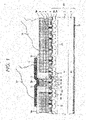
- FIG. 1 is a cross sectional view of a semiconductor device according to a first embodiment
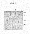
- FIG. 2 is a plan view of the same.
- FIG. 1 is the cross sectional view taken along a broken line A-A' in FIG. 2 .
- an n-type drift region 2 and an n-type drain region 1 having an impurity concentration higher than that of the drift region 2 are formed in a silicon carbide semiconductor substrate (hereinafter referred to as a semiconductor substrate) 40, and a drain electrode 13 made of a metal layer is formed on a back surface of the semiconductor substrate 40.
- a principal current cell 21, a current detection cell 22, and a gate control electrode 14 (see FIG. 2 ) that controls currents of the principal current cell 21 and the current detection cell 22 are disposed on the drift region 2.
- the principal current cell 21 is composed of P-well regions 3a each of which is formed on a part of the drift region 2, source regions 4a each of which is formed on a part of the P-well region 3a, gate oxide films 5 and gate electrodes 6 each of which is formed on the semiconductor substrate 40 adjacent to the source regions 4a, contacts 8 each of which is electrically connected to the P-well region 3a and the source regions 4a, and a source electrode 9a connected to the contacts 8.
- a positive voltage with respect to the source electrode 9a is applied to the drain electrode 13 and a positive voltage with respect to the source electrode 9a is applied to each of the gate electrodes 6, a current flows from the drain electrode 13 to the source electrode 9a in the principal current cell 21.
- the current detection cell 22 is composed of a P-well region 3b formed on a part of the drift region 2, source regions 4b each of which is formed on a part of the P-well region 3b, the gate oxide films 5 and the gate electrodes 6 each of which is formed on the semiconductor substrate 40 adjacent to the source regions 4b, the contact 8 electrically connected to the P-well region 3b and the source regions 4b, and a source electrode 9b connected to the contact 8.
- the source electrode 9b of the current detection cell 22 is electrically connected to a bonding pad wiring layer 12 formed on an interlayer insulating film 10 via a wiring layer contact 11.
- the bonding pad wiring layer 12 is formed with respect to the source electrode 9a of the principal current cell 21 so as to cover a part of the source electrode 9a via the interlayer insulating film 10.
- An electrically connected bonding pad portion 32 is formed on the bonding pad wiring layer 12 connected to the current detection cell 22. Therefore, in the current detection cell, when the voltage is applied to each of the gate electrodes 6, a detection current flows from the drain electrode 13 to the bonding pad portion 32 via the source electrode 9b. Bonding wires are integrally provided on the bonding pad portion 32.
- a part of the interlayer insulating film 10 on the source electrode 9a connected to the principal current cell 21 is opened, and a bonding pad portion 31 is formed on a part of the source electrode 9a.
- a principal current flows from the drain electrode 13 to the bonding pad portion 31 via the source electrode 9a. Bonding wires are integrally provided on the bonding pad portion 31.
- the gate electrodes 6 of the principal current cell 21 and the gate electrodes 6 of the current detection cell 22 are electrically connected with a polysilicon layer or the like constituting each of the gate electrodes 6, and are connected to a bonding pad portion for a gate via the gate control electrode 14.
- the current flowing through the current detection cell 22 has a current sense ratio of a constant ratio substantially equal to an area ratio on a plane with respect to the current flowing through the principal current cell 21.
- the current sense ratio is commonly set to about 1 : 1,000 to 1 : 50,000.
- an area of the current detection cell on the substrate plane is 1,600 ⁇ m 2 .
- This area is two orders of magnitude smaller than 400 x 400 ⁇ m 2 , which is an area of a bonding pad region necessary for connection of the bonding pad portion 32 of the semiconductor device.
- an area of the bonding pad wiring layer 12 to which the bonding pad portion 32 is connected on the substrate plane is made larger than the areas of the current detection cell 22 and the source electrode 9b. Since the bonding pad wiring layer 12 is provided so as to cover the source electrode 9b of the current detection cell 22 and a part of the source electrode 9a of the principal current cell 21, the source electrode 9b is miniaturized, and a size of the source electrode 9b is made substantially equal to a size of the current detection cell 22. Thus, the current detection cell 22 and the principal current cell 21 are disposed close to each other.
- the current detection cell 22 is disposed adjacent to the principal current cell 21, an element temperature during operation of the current detection cell 22 is brought close to an average element temperature during operation of the principal current cell 21 as compared with the conventional structure. Since the amount of the current of an element depends on the temperature, the current sense ratio between the current detection cell 22 and the principal current cell 21 changes when a temperature difference occurs. Therefore, with the present structure, a current accuracy in current detection is further improved.
- the current detection cell 22 is disposed adjacent to the principal current cell 21, the P-well regions 3a, 3b are not formed in regions away from the source electrodes 9a, 9b. Thus, when the element is switched from an on state to an off state, generation of a displacement current in the current detection cell is suppressed, and a noise current in the current detection cell is suppressed.
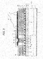
- FIG. 3 is a cross sectional view of a semiconductor device according to a second embodiment.
- FIG. 3 is the cross sectional view taken along the broken line A-A' in FIG. 2 .
- the same portions as those in the cross sectional view of the first embodiment illustrated in FIG. 1 are denoted by the same reference numerals, and the descriptions thereof will be omitted.
- the second embodiment is different from FIG. 1 of the first embodiment in that a bonding pad wiring layer 15 is formed on a part of the source electrode 9a connected to the principal current cell 21, and the bonding pad portion 31 is formed on the bonding pad wiring layer 15.
- the source electrodes 9a, 9b are formed of aluminum, and the bonding pad wiring layer 15 is formed of metal such as copper or nickel formed by a plating method similarly to the bonding pad wiring layer 12.
- material of the bonding pad wiring layer is optimally selected for the bonding pad portion such as copper, and reliability of the bonding pad portion is further enhanced.
- FIG. 4 is a plan view of a semiconductor device according to a third embodiment
- FIG. 5 is a cross sectional view of the same.
- FIG. 5 is the cross sectional view taken along a broken line B-B' in FIG. 4 .
- the same portions as those in the cross sectional view and the plan view of the first embodiment illustrated in FIGS. 1 and 2 are denoted by the same reference numerals, and the descriptions thereof will be omitted.
- the third embodiment is different from the first embodiment in that, as illustrated in FIG. 4 , the current detection cell 22 is not disposed under the bonding pad wiring layer 12 and is disposed at a position further close to a chip center. As illustrated in FIG. 5 , the current detection cell 22 and the bonding pad wiring layer 12 are connected to each other via the source electrode 9b and a routing wiring layer 16. Although the wire bonding connected to the source electrode 9a of the principal current cell 21 is closely arranged, an electrical short circuit is prevented by forming an insulating film 17 on the routing wiring layer 16.
- an arrangement position of the current detection cell in the chip is freely arranged without being restricted by an arrangement position of the bonding wire.
- FIG. 6 is a diagram illustrating a junction temperature distribution of the current detection cell, and shows the distribution of the junction temperatures of the principal current cell 21 and the current detection cell 22 in a broken line ⁇ - ⁇ ' of FIG. 2 and a broken line ⁇ - ⁇ ' of FIG. 4 .
- a horizontal axis represents a distance on the semiconductor device, and a vertical axis represents the junction temperature during element operation.
- the junction temperature of the principal current cell 21 is approximated by a quadratic function as illustrated in FIG. 6 , and becomes a maximum at a chip center position and becomes a minimum at a peripheral portion.
- a position A in FIG. 6 illustrates a case where the current detection cell 22 is located at the position illustrated in FIG. 2 of the first embodiment.
- a position B in FIG. 6 illustrates a case where the current detection cell 22 is located at the position illustrated in FIG. 4 of the third embodiment.
- the current detection cell 22 is disposed at the position illustrated in FIG.
- the bonding pad wiring layer 12 is disposed at an end of the principal current cell 21, and the current detection cell 22 is disposed at an arbitrarily optimum position of the principal current cell 21 via the routing wiring layer 16.
- the current detection cell 22 is also arranged at the center portion of the principal current cell 21, at which a maximum temperature of the chip is generated. As a result, the maximum temperature of the chip is detected with high accuracy by detecting the on-resistance of the current detection cell 22 and a forward voltage of a parasitic diode of the current detection cell 22.
- FIG. 7 is a plan view of a semiconductor device according to a fourth embodiment
- FIG. 8 is a cross sectional view taken along a broken line C-C' in FIG. 7
- FIG. 9 is a cross sectional view taken along a broken line D-D' in FIG. 7 .
- the same portions as those in the cross sectional view and the plan view of the first embodiment illustrated in FIGS. 1 and 2 are denoted by the same reference numerals, and the descriptions thereof will be omitted.
- the gate control electrode 14 is the bonding pad region, and the bonding pad portion is connected on the gate control electrode 14.
- the gate control electrode 14 is connected to a bonding pad wiring layer 19 formed on the interlayer insulating film 10 on the gate control electrode 14 via a wiring layer contact 18.
- a wiring layer of the gate electrode 6 connected to a gate of the principal current cell is illustrated in FIG. 8
- a wiring layer of the contact 8 and the source region 4a is illustrated in FIG. 9 .
- An area on the plane of the gate control electrode 14 is smaller than an area of the bonding pad wiring layer 19, and the principal current cell 21 and the source electrode 9a of the principal current cell are disposed under a part of the bonding pad wiring layer 19 connected to a gate cell 23.
- the bonding pad wiring layer 19 is connected to the gate control electrode 14, and is formed with respect to the source electrode 9a so as to cover a part of the source electrode 9a via the interlayer insulating film 10.
- the gate cell 23 controls the amount of current output from the principal current cell 21.
- the gate control electrode 14 is the same as that of the other embodiments in that the gate control electrode 14 is connected to the gate electrodes 6 of the principal current cell 21 and the current detection cell 22 with the polysilicon layer constituting the gate electrode 6.
- the bonding pad wiring layer 19 is provided on the gate control electrode 14, the area on the plane of the gate control, electrode 14 is made smaller than the area of the bonding pad wiring layer 19, and the principal current cell 21 and the source electrode 9a of the principal current cell is arranged close to the gate control electrode 14. Therefore, the area on the plane of the principal current cell is further enhanced. As a result, the on-resistance of the principal current cell is reduced, and performance is further improved. In addition, when the area on the plane of the principal current cell is fixed, a chip area is reduced, and the chip cost is reduced.
- a semiconductor substrate made of such as silicon, gallium nitride, gallium oxide, or diamond is also used.
- the semiconductor substrate made of the silicon carbide, the gallium nitride, the gallium oxide, or the diamond a ratio of the cost of the semiconductor substrate to the total chip cost is large, so that the chip cost is effectively reduced.
- the bonding pad portion and the bonding wires may be connected with a lead frame made of copper or the like and soldering or the like.
- the semiconductor device includes the semiconductor substrate 40 having a first main surface and a second main surface; the principal current cell formed on the semiconductor substrate 40 and having the source electrode 9a formed on the first main surface and the drain electrode 13 formed on the second main surface; a sub-cell (the current detection cell 22, the gate cell 23) formed on the first main surface and having a third electrode (the gate control electrode 14, the source electrode 9b) formed at a position of the same height as the source electrode 9a with respect to the semiconductor substrate 40; the bonding pad wiring layer 12 connected to the third electrode (the gate control electrode 14, the source electrode 9b) and formed with respect to the source electrode 9a so as to cover a part of the source electrode 9a via the interlayer insulating film; and the bonding pad portion 32 connected to the first bonding pad wiring layer 12.
- the area of the principal current cell is increased regardless of the area of the bonding pad wiring layer for the sub-cell.
Landscapes
- Semiconductor Integrated Circuits (AREA)
Abstract
Description
- The present invention relates to a semiconductor device.
- A semiconductor device having a structure in which a principal current cell and a sub-cell (such as a current detection cell) are disposed on the same substrate has been known.
PTL 1 discloses a metal-oxide-semiconductor field-effect transistor (MOSFET) semiconductor device in which a principal current cell and a current detection cell are disposed on the same substrate. In the MOSFET semiconductor device, a current detection bonding pad wiring layer connected to the current detection cell is formed above the current detection cell, and a source pad wiring layer connected to the principal current cell is formed in a region excluding a region where the current detection bonding pad wiring layer is formed. - PTL 1:
WO 2011/161721 A - According to the technique disclosed in
PTL 1, there is a problem that an area of the principal current cell is reduced by an area of the bonding pad wiring layer for the sub-cell. - A semiconductor device according to the present invention includes: a semiconductor substrate having a first main surface and a second main surface; a principal current cell formed on the semiconductor substrate and having a first electrode formed on the first main surface and a second electrode formed on the second main surface; a sub-cell formed on the first main surface and having a third electrode formed at a position of the same height as the first electrode with respect to the semiconductor substrate; a first bonding pad wiring layer connected to the third electrode and formed with respect to the first electrode so as to cover a part of the first electrode via an interlayer insulating film; and a first bonding pad portion connected to the first bonding pad wiring layer.
- According to the present invention, the area of the principal current cell is increased regardless of the area of the bonding pad wiring layer for the sub-cell.
-
- [
FIG. 1] FIG. 1 is a cross sectional view illustrating a semiconductor device according to a first embodiment. - [
FIG. 2] FIG. 2 is a plan view illustrating the semiconductor device according to the first embodiment. - [
FIG. 3] FIG. 3 is a cross sectional view illustrating a semiconductor device according to a second embodiment. - [
FIG. 4] FIG. 4 is a plan view illustrating a semiconductor device according to a third embodiment. - [
FIG. 5] FIG. 5 is a cross sectional view illustrating the semiconductor device according to the third embodiment. - [
FIG. 6] FIG. 6 is a diagram illustrating a junction temperature distribution of a current detection cell. - [
FIG. 7] FIG. 7 is a plan view illustrating a semiconductor device according to a fourth embodiment. - [
FIG. 8] FIG. 8 is a cross sectional view illustrating the semiconductor device according to the fourth embodiment. - [
FIG. 9] FIG. 9 is a cross sectional view illustrating the semiconductor device according to the fourth embodiment. - Embodiments of the present invention will be hereinafter described with reference to the drawings. In the embodiments, as an example of a semiconductor device, a power semiconductor device that mainly includes an n-type channel silicon carbide MOSFET incorporating a current detection element will be described. In each of the drawings, the same components will be denoted by the same reference numerals, and redundant descriptions will be omitted.
-
FIG. 1 is a cross sectional view of a semiconductor device according to a first embodiment, andFIG. 2 is a plan view of the same.FIG. 1 is the cross sectional view taken along a broken line A-A' inFIG. 2 . - As shown in
FIG. 1 , an n-type drift region 2 and an n-type drain region 1 having an impurity concentration higher than that of thedrift region 2 are formed in a silicon carbide semiconductor substrate (hereinafter referred to as a semiconductor substrate) 40, and adrain electrode 13 made of a metal layer is formed on a back surface of thesemiconductor substrate 40. A principalcurrent cell 21, acurrent detection cell 22, and a gate control electrode 14 (seeFIG. 2 ) that controls currents of the principalcurrent cell 21 and thecurrent detection cell 22 are disposed on thedrift region 2. - As shown in
FIG. 1 , the principalcurrent cell 21 is composed of P-well regions 3a each of which is formed on a part of thedrift region 2,source regions 4a each of which is formed on a part of the P-well region 3a,gate oxide films 5 andgate electrodes 6 each of which is formed on thesemiconductor substrate 40 adjacent to thesource regions 4a,contacts 8 each of which is electrically connected to the P-well region 3a and thesource regions 4a, and asource electrode 9a connected to thecontacts 8. In the above state, when a positive voltage with respect to thesource electrode 9a is applied to thedrain electrode 13 and a positive voltage with respect to thesource electrode 9a is applied to each of thegate electrodes 6, a current flows from thedrain electrode 13 to thesource electrode 9a in the principalcurrent cell 21. - The
current detection cell 22 is composed of a P-well region 3b formed on a part of thedrift region 2,source regions 4b each of which is formed on a part of the P-well region 3b, thegate oxide films 5 and thegate electrodes 6 each of which is formed on thesemiconductor substrate 40 adjacent to thesource regions 4b, thecontact 8 electrically connected to the P-well region 3b and thesource regions 4b, and asource electrode 9b connected to thecontact 8. - The
source electrode 9b of thecurrent detection cell 22 is electrically connected to a bondingpad wiring layer 12 formed on aninterlayer insulating film 10 via awiring layer contact 11. The bondingpad wiring layer 12 is formed with respect to thesource electrode 9a of the principalcurrent cell 21 so as to cover a part of thesource electrode 9a via theinterlayer insulating film 10. - An electrically connected
bonding pad portion 32 is formed on the bondingpad wiring layer 12 connected to thecurrent detection cell 22. Therefore, in the current detection cell, when the voltage is applied to each of thegate electrodes 6, a detection current flows from thedrain electrode 13 to thebonding pad portion 32 via thesource electrode 9b. Bonding wires are integrally provided on thebonding pad portion 32. - Further, a part of the
interlayer insulating film 10 on thesource electrode 9a connected to the principalcurrent cell 21 is opened, and abonding pad portion 31 is formed on a part of thesource electrode 9a. Thus, in the principal current cell, a principal current flows from thedrain electrode 13 to thebonding pad portion 31 via thesource electrode 9a. Bonding wires are integrally provided on thebonding pad portion 31. - Although not illustrated, the
gate electrodes 6 of the principalcurrent cell 21 and thegate electrodes 6 of thecurrent detection cell 22 are electrically connected with a polysilicon layer or the like constituting each of thegate electrodes 6, and are connected to a bonding pad portion for a gate via thegate control electrode 14. - When potentials of the
source electrode 9a of the principalcurrent cell 21 and thesource electrode 9b of thecurrent detection cell 22 are equalized, the current flowing through thecurrent detection cell 22 has a current sense ratio of a constant ratio substantially equal to an area ratio on a plane with respect to the current flowing through the principalcurrent cell 21. The current sense ratio is commonly set to about 1 : 1,000 to 1 : 50,000. For example, when the current sense ratio is 1 : 10,000 and an area of the principal current cell on a substrate plane is 16 mm2, an area of the current detection cell on the substrate plane is 1,600 µm2. This area is two orders of magnitude smaller than 400 x 400 µm2, which is an area of a bonding pad region necessary for connection of thebonding pad portion 32 of the semiconductor device. Therefore, as illustrated inFIG. 2 , an area of the bondingpad wiring layer 12 to which thebonding pad portion 32 is connected on the substrate plane is made larger than the areas of thecurrent detection cell 22 and thesource electrode 9b. Since the bondingpad wiring layer 12 is provided so as to cover thesource electrode 9b of thecurrent detection cell 22 and a part of thesource electrode 9a of the principalcurrent cell 21, thesource electrode 9b is miniaturized, and a size of thesource electrode 9b is made substantially equal to a size of thecurrent detection cell 22. Thus, thecurrent detection cell 22 and the principalcurrent cell 21 are disposed close to each other. - As a result, an increase in on-resistance due to a decrease in the area of the principal
current cell 21 and an increase in chip cost due to an increase in chip size by providing thecurrent detection cell 22 are suppressed. As compared with the conventional structure, a manufacturing cost of a wafer increases by forming the bondingpad wiring layer 12. However, a cost of a silicon semiconductor substrate accounts for a relatively large proportion of the total cost. Therefore, the present structure in which the increase in the chip size is suppressed and the number of chips acquired per wafer is increased reduces the chip cost as compared with the conventional structure. - In addition, since the
current detection cell 22 is disposed adjacent to the principalcurrent cell 21, an element temperature during operation of thecurrent detection cell 22 is brought close to an average element temperature during operation of the principalcurrent cell 21 as compared with the conventional structure. Since the amount of the current of an element depends on the temperature, the current sense ratio between thecurrent detection cell 22 and the principalcurrent cell 21 changes when a temperature difference occurs. Therefore, with the present structure, a current accuracy in current detection is further improved. - Further, since the
current detection cell 22 is disposed adjacent to the principalcurrent cell 21, the P-well regions source electrodes -
FIG. 3 is a cross sectional view of a semiconductor device according to a second embodiment.FIG. 3 is the cross sectional view taken along the broken line A-A' inFIG. 2 . The same portions as those in the cross sectional view of the first embodiment illustrated inFIG. 1 are denoted by the same reference numerals, and the descriptions thereof will be omitted. - The second embodiment is different from
FIG. 1 of the first embodiment in that a bondingpad wiring layer 15 is formed on a part of thesource electrode 9a connected to the principalcurrent cell 21, and thebonding pad portion 31 is formed on the bondingpad wiring layer 15. Thesource electrodes pad wiring layer 15 is formed of metal such as copper or nickel formed by a plating method similarly to the bondingpad wiring layer 12. As compared with the case where an aluminum metal bonding pad portion is formed on thesource electrodes -
FIG. 4 is a plan view of a semiconductor device according to a third embodiment, andFIG. 5 is a cross sectional view of the same.FIG. 5 is the cross sectional view taken along a broken line B-B' inFIG. 4 . The same portions as those in the cross sectional view and the plan view of the first embodiment illustrated inFIGS. 1 and2 are denoted by the same reference numerals, and the descriptions thereof will be omitted. - The third embodiment is different from the first embodiment in that, as illustrated in
FIG. 4 , thecurrent detection cell 22 is not disposed under the bondingpad wiring layer 12 and is disposed at a position further close to a chip center. As illustrated inFIG. 5 , thecurrent detection cell 22 and the bondingpad wiring layer 12 are connected to each other via thesource electrode 9b and arouting wiring layer 16. Although the wire bonding connected to thesource electrode 9a of the principalcurrent cell 21 is closely arranged, an electrical short circuit is prevented by forming an insulatingfilm 17 on therouting wiring layer 16. - According to the present embodiment, as compared with the first embodiment, an arrangement position of the current detection cell in the chip is freely arranged without being restricted by an arrangement position of the bonding wire.
-
FIG. 6 is a diagram illustrating a junction temperature distribution of the current detection cell, and shows the distribution of the junction temperatures of the principalcurrent cell 21 and thecurrent detection cell 22 in a broken line α-α' ofFIG. 2 and a broken line β-β' ofFIG. 4 . A horizontal axis represents a distance on the semiconductor device, and a vertical axis represents the junction temperature during element operation. - When a power density per unit area during the operation of the principal
current cell 21 and thecurrent detection cell 22 is uniform, the junction temperature of the principalcurrent cell 21 is approximated by a quadratic function as illustrated inFIG. 6 , and becomes a maximum at a chip center position and becomes a minimum at a peripheral portion. A position A inFIG. 6 illustrates a case where thecurrent detection cell 22 is located at the position illustrated inFIG. 2 of the first embodiment. A position B inFIG. 6 illustrates a case where thecurrent detection cell 22 is located at the position illustrated inFIG. 4 of the third embodiment. Thecurrent detection cell 22 is disposed at the position illustrated inFIG. 4 , that is, such that an average temperature of the principalcurrent cell 21 and the temperature of thecurrent detection cell 22 are substantially equal when the current flows through the principalcurrent cell 21 and thecurrent detection cell 22. As a result, as compared with the first embodiment, the element temperature during the operation of thecurrent detection cell 22 is brought further close to the average element temperature during the operation of the principalcurrent cell 21, and the current accuracy in the current detection is further improved. As described above, the bondingpad wiring layer 12 is disposed at an end of the principalcurrent cell 21, and thecurrent detection cell 22 is disposed at an arbitrarily optimum position of the principalcurrent cell 21 via therouting wiring layer 16. - The
current detection cell 22 is also arranged at the center portion of the principalcurrent cell 21, at which a maximum temperature of the chip is generated. As a result, the maximum temperature of the chip is detected with high accuracy by detecting the on-resistance of thecurrent detection cell 22 and a forward voltage of a parasitic diode of thecurrent detection cell 22. -
FIG. 7 is a plan view of a semiconductor device according to a fourth embodiment,FIG. 8 is a cross sectional view taken along a broken line C-C' inFIG. 7 , andFIG. 9 is a cross sectional view taken along a broken line D-D' inFIG. 7 . The same portions as those in the cross sectional view and the plan view of the first embodiment illustrated inFIGS. 1 and2 are denoted by the same reference numerals, and the descriptions thereof will be omitted. - In the first embodiment, as illustrated in
FIG. 2 , thegate control electrode 14 is the bonding pad region, and the bonding pad portion is connected on thegate control electrode 14. On the other hand, in the present embodiment, as illustrated inFIGS. 7 ,8 , and9 , thegate control electrode 14 is connected to a bondingpad wiring layer 19 formed on theinterlayer insulating film 10 on thegate control electrode 14 via awiring layer contact 18. A wiring layer of thegate electrode 6 connected to a gate of the principal current cell is illustrated inFIG. 8 , and a wiring layer of thecontact 8 and thesource region 4a is illustrated inFIG. 9 . An area on the plane of thegate control electrode 14 is smaller than an area of the bondingpad wiring layer 19, and the principalcurrent cell 21 and thesource electrode 9a of the principal current cell are disposed under a part of the bondingpad wiring layer 19 connected to agate cell 23. In other words, the bondingpad wiring layer 19 is connected to thegate control electrode 14, and is formed with respect to thesource electrode 9a so as to cover a part of thesource electrode 9a via theinterlayer insulating film 10. Thegate cell 23 controls the amount of current output from the principalcurrent cell 21. Thegate control electrode 14 is the same as that of the other embodiments in that thegate control electrode 14 is connected to thegate electrodes 6 of the principalcurrent cell 21 and thecurrent detection cell 22 with the polysilicon layer constituting thegate electrode 6. - Since the bonding
pad wiring layer 19 is provided on thegate control electrode 14, the area on the plane of the gate control,electrode 14 is made smaller than the area of the bondingpad wiring layer 19, and the principalcurrent cell 21 and thesource electrode 9a of the principal current cell is arranged close to thegate control electrode 14. Therefore, the area on the plane of the principal current cell is further enhanced. As a result, the on-resistance of the principal current cell is reduced, and performance is further improved. In addition, when the area on the plane of the principal current cell is fixed, a chip area is reduced, and the chip cost is reduced. - Although in each of the above embodiments, the semiconductor device using the silicon
carbide semiconductor substrate 40 has been described, a semiconductor substrate made of such as silicon, gallium nitride, gallium oxide, or diamond is also used. In particular, in the semiconductor substrate made of the silicon carbide, the gallium nitride, the gallium oxide, or the diamond, a ratio of the cost of the semiconductor substrate to the total chip cost is large, so that the chip cost is effectively reduced. - Although the semiconductor device is externally connected with the bonding pad portion and the bonding wires, the bonding pad portion and the bonding wires may be connected with a lead frame made of copper or the like and soldering or the like.
- According to the embodiments described above, the following effect is obtained.
- (1) The semiconductor device includes the
semiconductor substrate 40 having a first main surface and a second main surface; the principal current cell formed on thesemiconductor substrate 40 and having thesource electrode 9a formed on the first main surface and thedrain electrode 13 formed on the second main surface; a sub-cell (thecurrent detection cell 22, the gate cell 23) formed on the first main surface and having a third electrode (thegate control electrode 14, thesource electrode 9b) formed at a position of the same height as thesource electrode 9a with respect to thesemiconductor substrate 40; the bondingpad wiring layer 12 connected to the third electrode (thegate control electrode 14, thesource electrode 9b) and formed with respect to thesource electrode 9a so as to cover a part of thesource electrode 9a via the interlayer insulating film; and thebonding pad portion 32 connected to the first bondingpad wiring layer 12. According to the above structure, the area of the principal current cell is increased regardless of the area of the bonding pad wiring layer for the sub-cell. - It is to be understood that the present invention is not limited to the above embodiments, and other forms conceivable within the scope of the technical idea of the present invention are also included within the scope of the present invention as long as the features of the present invention are not impaired.
-
- 1
- N+ type drain region
- 2
- N- type drain drift region
- 3a
- P-well region of principal current cell
- 3b
- P-well region of current detection cell
- 4a
- N+ source region of principal current cell
- 4b
- N+ source region of current detection cell
- 5
- gate oxide film
- 6
- gate electrode
- 7
- interlayer insulating film
- 8
- contact
- 9a
- source electrode of principal current cell
- 9b
- source electrode of current detection cell
- 10
- interlayer insulating film
- 11
- wiring layer contact
- 12
- bonding pad wiring layer
- 13
- drain electrode
- 14
- gate control electrode
- 15
- bonding pad wiring layer
- 16
- routing wiring layer
- 17
- insulating film
- 18
- wiring layer contact
- 19
- bonding pad wiring layer
- 21
- principal current cell
- 22
- current detection cell
- 23
- gate cell
- 31, 32, 33
- bonding pad portion
- 40
- silicon carbide semiconductor substrate
Claims (8)
- A semiconductor device comprising:a semiconductor substrate having a first main surface and a second main surface;a principal current cell formed on the semiconductor substrate and including a first electrode formed on the first main surface and a second electrode formed on the second main surface;a sub-cell formed on the first main surface and including a third electrode formed at a position of the same height as the first electrode with respect to the semiconductor substrate;a first bonding pad wiring layer connected to the third electrode and formed with respect to the first electrode so as to cover a part of the first electrode via an interlayer insulating film; anda first bonding pad portion connected to the first bonding pad wiring layer.
- The semiconductor device according to claim 1, wherein
the sub-cell is a current detection cell that detects an amount of current corresponding to an amount of current output from the principal current cell. - The semiconductor device according to claim 1, wherein
the sub-cell is a gate cell that controls the amount of current output from the principal current cell. - The semiconductor device according to claim 2 or 3, wherein
a plane size of the sub-cell with respect to the semiconductor substrate is smaller than a plane size of the first bonding pad portion with respect to the first bonding pad wiring layer. - The semiconductor device according to claim 2, wherein
the current detection cell is surrounded on all sides by the principal current cell. - The semiconductor device according to claim 2, wherein
the current detection cell is disposed closer to a central portion of the semiconductor substrate than the first bonding pad portion connected to the current detection cell. - The semiconductor device according to claim 2, wherein
the current detection cell is disposed so as to make an average temperature of the principal current cell and a temperature of the current detection cell substantially equal when current flows through the principal current cell and the current detection cell. - The semiconductor device according to claim 1, wherein
a second bonding pad wiring layer is formed on a part of the first electrode, the first electrode and the second bonding pad wiring layer are electrically connected, and a second bonding pad portion is connected to the second bonding pad wiring layer.
Applications Claiming Priority (2)
| Application Number | Priority Date | Filing Date | Title |
|---|---|---|---|
| JP2019110944A JP7145817B2 (en) | 2019-06-14 | 2019-06-14 | semiconductor equipment |
| PCT/JP2020/022617 WO2020250869A1 (en) | 2019-06-14 | 2020-06-09 | Semiconductor device |
Publications (2)
| Publication Number | Publication Date |
|---|---|
| EP3985716A1 true EP3985716A1 (en) | 2022-04-20 |
| EP3985716A4 EP3985716A4 (en) | 2023-06-28 |
Family
ID=73780962
Family Applications (1)
| Application Number | Title | Priority Date | Filing Date |
|---|---|---|---|
| EP20823491.4A Pending EP3985716A4 (en) | 2019-06-14 | 2020-06-09 | Semiconductor device |
Country Status (4)
| Country | Link |
|---|---|
| US (1) | US11855166B2 (en) |
| EP (1) | EP3985716A4 (en) |
| JP (1) | JP7145817B2 (en) |
| WO (1) | WO2020250869A1 (en) |
Families Citing this family (4)
| Publication number | Priority date | Publication date | Assignee | Title |
|---|---|---|---|---|
| JP7497719B2 (en) * | 2021-12-16 | 2024-06-11 | 株式会社三洋物産 | Gaming Machines |
| JP7497720B2 (en) * | 2021-12-16 | 2024-06-11 | 株式会社三洋物産 | Gaming Machines |
| JP7497718B2 (en) * | 2021-12-16 | 2024-06-11 | 株式会社三洋物産 | Gaming Machines |
| WO2026005481A1 (en) * | 2024-06-26 | 2026-01-02 | 주식회사 엘엑스세미콘 | Power semiconductor device and power semiconductor module |
Family Cites Families (14)
| Publication number | Priority date | Publication date | Assignee | Title |
|---|---|---|---|---|
| JPH0252468A (en) * | 1988-08-17 | 1990-02-22 | Mitsubishi Electric Corp | Semiconductor device |
| JPH0831606B2 (en) * | 1989-11-17 | 1996-03-27 | 株式会社東芝 | High power semiconductor device |
| JP3338185B2 (en) * | 1994-08-02 | 2002-10-28 | 株式会社東芝 | Semiconductor device |
| JP3062029B2 (en) * | 1995-01-31 | 2000-07-10 | 日本電気株式会社 | Temperature detection method using forward voltage of diode |
| JP2004014707A (en) * | 2002-06-05 | 2004-01-15 | Renesas Technology Corp | Semiconductor device |
| US20060055056A1 (en) * | 2003-11-21 | 2006-03-16 | Denso Corporation | Semiconductor equipment having a pair of heat radiation plates |
| JP4955222B2 (en) * | 2005-05-20 | 2012-06-20 | ルネサスエレクトロニクス株式会社 | Manufacturing method of semiconductor device |
| JP5369300B2 (en) * | 2009-09-16 | 2013-12-18 | 三菱電機株式会社 | Semiconductor device and manufacturing method thereof |
| JP4962665B2 (en) * | 2010-04-06 | 2012-06-27 | 三菱電機株式会社 | Power semiconductor device, manufacturing method thereof, and power module |
| WO2011161721A1 (en) * | 2010-06-24 | 2011-12-29 | 三菱電機株式会社 | Power semiconductor device |
| JP6218462B2 (en) * | 2013-07-04 | 2017-10-25 | 三菱電機株式会社 | Wide gap semiconductor device |
| JP6510310B2 (en) * | 2014-05-12 | 2019-05-08 | ローム株式会社 | Semiconductor device |
| JP2017005153A (en) * | 2015-06-11 | 2017-01-05 | ルネサスエレクトロニクス株式会社 | Semiconductor device |
| WO2019106948A1 (en) * | 2017-11-30 | 2019-06-06 | 住友電気工業株式会社 | Gate insulation-type transistor |
-
2019
- 2019-06-14 JP JP2019110944A patent/JP7145817B2/en active Active
-
2020
- 2020-06-09 WO PCT/JP2020/022617 patent/WO2020250869A1/en not_active Ceased
- 2020-06-09 EP EP20823491.4A patent/EP3985716A4/en active Pending
- 2020-06-09 US US17/618,763 patent/US11855166B2/en active Active
Also Published As
| Publication number | Publication date |
|---|---|
| JP2020205298A (en) | 2020-12-24 |
| EP3985716A4 (en) | 2023-06-28 |
| US11855166B2 (en) | 2023-12-26 |
| WO2020250869A1 (en) | 2020-12-17 |
| US20220359694A1 (en) | 2022-11-10 |
| JP7145817B2 (en) | 2022-10-03 |
Similar Documents
| Publication | Publication Date | Title |
|---|---|---|
| US12052014B2 (en) | Semiconductor device | |
| US10811499B2 (en) | Wide bandgap semiconductor device including transistor cells and compensation structure | |
| CN112786591B (en) | Semiconductor device | |
| JP4097417B2 (en) | Semiconductor device | |
| US11855166B2 (en) | Semiconductor device including sub-cell disposed at chip center | |
| US11371891B2 (en) | Semiconductor device, semiconductor package, semiconductor module, and semiconductor circuit device | |
| JP7529750B2 (en) | Semiconductor device and power module | |
| JP7825764B2 (en) | Semiconductor Devices | |
| KR102576366B1 (en) | Transistor semiconductor die with increased active area | |
| US11658093B2 (en) | Semiconductor element with electrode having first section and second sections in contact with the first section, and semiconductor device | |
| JP6746978B2 (en) | Semiconductor device | |
| CN114068715A (en) | Semiconductor device with a plurality of semiconductor chips | |
| US11245007B2 (en) | Wide-bandgap semiconductor device including gate fingers between bond pads | |
| US10978588B2 (en) | Semiconductor device | |
| CN117673128A (en) | Semiconductor device | |
| US20240274697A1 (en) | Semiconductor device and method of manufacturing the same | |
| US12610864B2 (en) | Semiconductor device | |
| US12519074B2 (en) | Semiconductor chip and semiconductor device | |
| JP7052826B2 (en) | Semiconductor device | |
| US20250185318A1 (en) | Semiconductor device and semiconductor module | |
| JP2005209828A (en) | Semiconductor device |
Legal Events
| Date | Code | Title | Description |
|---|---|---|---|
| STAA | Information on the status of an ep patent application or granted ep patent |
Free format text: STATUS: THE INTERNATIONAL PUBLICATION HAS BEEN MADE |
|
| PUAI | Public reference made under article 153(3) epc to a published international application that has entered the european phase |
Free format text: ORIGINAL CODE: 0009012 |
|
| STAA | Information on the status of an ep patent application or granted ep patent |
Free format text: STATUS: REQUEST FOR EXAMINATION WAS MADE |
|
| 17P | Request for examination filed |
Effective date: 20220114 |
|
| AK | Designated contracting states |
Kind code of ref document: A1 Designated state(s): AL AT BE BG CH CY CZ DE DK EE ES FI FR GB GR HR HU IE IS IT LI LT LU LV MC MK MT NL NO PL PT RO RS SE SI SK SM TR |
|
| DAV | Request for validation of the european patent (deleted) | ||
| DAX | Request for extension of the european patent (deleted) | ||
| A4 | Supplementary search report drawn up and despatched |
Effective date: 20230525 |
|
| RIC1 | Information provided on ipc code assigned before grant |
Ipc: H01L 27/088 20060101ALN20230519BHEP Ipc: H01L 21/8234 20060101ALN20230519BHEP Ipc: H01L 29/06 20060101ALI20230519BHEP Ipc: H01L 23/00 20060101ALI20230519BHEP Ipc: H01L 29/12 20060101ALI20230519BHEP Ipc: H01L 29/78 20060101ALI20230519BHEP Ipc: H01L 27/04 20060101ALI20230519BHEP Ipc: H01L 21/822 20060101AFI20230519BHEP |
|
| STAA | Information on the status of an ep patent application or granted ep patent |
Free format text: STATUS: EXAMINATION IS IN PROGRESS |
|
| 17Q | First examination report despatched |
Effective date: 20250206 |
|
| RAP3 | Party data changed (applicant data changed or rights of an application transferred) |
Owner name: ASTEMO, LTD. |