EP3982401A1 - Plate for a power module with semiconductor die and pin holder welded thereto - Google Patents
Plate for a power module with semiconductor die and pin holder welded thereto Download PDFInfo
- Publication number
- EP3982401A1 EP3982401A1 EP21201233.0A EP21201233A EP3982401A1 EP 3982401 A1 EP3982401 A1 EP 3982401A1 EP 21201233 A EP21201233 A EP 21201233A EP 3982401 A1 EP3982401 A1 EP 3982401A1
- Authority
- EP
- European Patent Office
- Prior art keywords
- flange
- blocking element
- pin
- pin blocking
- bearing plate
- Prior art date
- Legal status (The legal status is an assumption and is not a legal conclusion. Google has not performed a legal analysis and makes no representation as to the accuracy of the status listed.)
- Granted
Links
Images


Classifications
-
- H—ELECTRICITY
- H10—SEMICONDUCTOR DEVICES; ELECTRIC SOLID-STATE DEVICES NOT OTHERWISE PROVIDED FOR
- H10W—GENERIC PACKAGES, INTERCONNECTIONS, CONNECTORS OR OTHER CONSTRUCTIONAL DETAILS OF DEVICES COVERED BY CLASS H10
- H10W76/00—Containers; Fillings or auxiliary members therefor; Seals
- H10W76/10—Containers or parts thereof
- H10W76/12—Containers or parts thereof characterised by their shape
- H10W76/15—Containers comprising an insulating or insulated base
-
- H—ELECTRICITY
- H10—SEMICONDUCTOR DEVICES; ELECTRIC SOLID-STATE DEVICES NOT OTHERWISE PROVIDED FOR
- H10W—GENERIC PACKAGES, INTERCONNECTIONS, CONNECTORS OR OTHER CONSTRUCTIONAL DETAILS OF DEVICES COVERED BY CLASS H10
- H10W72/00—Interconnections or connectors in packages
- H10W72/50—Bond wires
-
- H—ELECTRICITY
- H01—ELECTRIC ELEMENTS
- H01R—ELECTRICALLY-CONDUCTIVE CONNECTIONS; STRUCTURAL ASSOCIATIONS OF A PLURALITY OF MUTUALLY-INSULATED ELECTRICAL CONNECTING ELEMENTS; COUPLING DEVICES; CURRENT COLLECTORS
- H01R12/00—Structural associations of a plurality of mutually-insulated electrical connecting elements, specially adapted for printed circuits, e.g. printed circuit boards [PCB], flat or ribbon cables, or like generally planar structures, e.g. terminal strips, terminal blocks; Coupling devices specially adapted for printed circuits, flat or ribbon cables, or like generally planar structures; Terminals specially adapted for contact with, or insertion into, printed circuits, flat or ribbon cables, or like generally planar structures
- H01R12/50—Fixed connections
- H01R12/51—Fixed connections for rigid printed circuits or like structures
- H01R12/55—Fixed connections for rigid printed circuits or like structures characterised by the terminals
- H01R12/58—Fixed connections for rigid printed circuits or like structures characterised by the terminals terminals for insertion into holes
- H01R12/585—Terminals having a press fit or a compliant portion and a shank passing through a hole in the printed circuit board
-
- H—ELECTRICITY
- H01—ELECTRIC ELEMENTS
- H01R—ELECTRICALLY-CONDUCTIVE CONNECTIONS; STRUCTURAL ASSOCIATIONS OF A PLURALITY OF MUTUALLY-INSULATED ELECTRICAL CONNECTING ELEMENTS; COUPLING DEVICES; CURRENT COLLECTORS
- H01R43/00—Apparatus or processes specially adapted for manufacturing, assembling, maintaining, or repairing of line connectors or current collectors or for joining electric conductors
- H01R43/02—Apparatus or processes specially adapted for manufacturing, assembling, maintaining, or repairing of line connectors or current collectors or for joining electric conductors for soldered or welded connections
- H01R43/0207—Ultrasonic-, H.F.-, cold- or impact welding
-
- H—ELECTRICITY
- H05—ELECTRIC TECHNIQUES NOT OTHERWISE PROVIDED FOR
- H05K—PRINTED CIRCUITS; CASINGS OR CONSTRUCTIONAL DETAILS OF ELECTRIC APPARATUS; MANUFACTURE OF ASSEMBLAGES OF ELECTRICAL COMPONENTS
- H05K3/00—Apparatus or processes for manufacturing printed circuits
- H05K3/40—Forming printed elements for providing electric connections to or between printed circuits
- H05K3/4007—Surface contacts, e.g. bumps
- H05K3/4015—Surface contacts, e.g. bumps using auxiliary conductive elements, e.g. pieces of metal foil, metallic spheres
-
- H—ELECTRICITY
- H10—SEMICONDUCTOR DEVICES; ELECTRIC SOLID-STATE DEVICES NOT OTHERWISE PROVIDED FOR
- H10W—GENERIC PACKAGES, INTERCONNECTIONS, CONNECTORS OR OTHER CONSTRUCTIONAL DETAILS OF DEVICES COVERED BY CLASS H10
- H10W40/00—Arrangements for thermal protection or thermal control
- H10W40/20—Arrangements for cooling
- H10W40/25—Arrangements for cooling characterised by their materials
- H10W40/255—Arrangements for cooling characterised by their materials having a laminate or multilayered structure, e.g. direct bond copper [DBC] ceramic substrates
-
- H—ELECTRICITY
- H10—SEMICONDUCTOR DEVICES; ELECTRIC SOLID-STATE DEVICES NOT OTHERWISE PROVIDED FOR
- H10W—GENERIC PACKAGES, INTERCONNECTIONS, CONNECTORS OR OTHER CONSTRUCTIONAL DETAILS OF DEVICES COVERED BY CLASS H10
- H10W70/00—Package substrates; Interposers; Redistribution layers [RDL]
- H10W70/20—Conductive package substrates serving as an interconnection, e.g. metal plates
-
- H—ELECTRICITY
- H10—SEMICONDUCTOR DEVICES; ELECTRIC SOLID-STATE DEVICES NOT OTHERWISE PROVIDED FOR
- H10W—GENERIC PACKAGES, INTERCONNECTIONS, CONNECTORS OR OTHER CONSTRUCTIONAL DETAILS OF DEVICES COVERED BY CLASS H10
- H10W70/00—Package substrates; Interposers; Redistribution layers [RDL]
- H10W70/60—Insulating or insulated package substrates; Interposers; Redistribution layers
- H10W70/62—Insulating or insulated package substrates; Interposers; Redistribution layers characterised by their interconnections
- H10W70/65—Shapes or dispositions of interconnections
- H10W70/658—Shapes or dispositions of interconnections for devices provided for in groups H10D8/00 - H10D48/00
-
- H—ELECTRICITY
- H10—SEMICONDUCTOR DEVICES; ELECTRIC SOLID-STATE DEVICES NOT OTHERWISE PROVIDED FOR
- H10W—GENERIC PACKAGES, INTERCONNECTIONS, CONNECTORS OR OTHER CONSTRUCTIONAL DETAILS OF DEVICES COVERED BY CLASS H10
- H10W90/00—Package configurations
- H10W90/701—Package configurations characterised by the relative positions of pads or connectors relative to package parts
-
- H—ELECTRICITY
- H05—ELECTRIC TECHNIQUES NOT OTHERWISE PROVIDED FOR
- H05K—PRINTED CIRCUITS; CASINGS OR CONSTRUCTIONAL DETAILS OF ELECTRIC APPARATUS; MANUFACTURE OF ASSEMBLAGES OF ELECTRICAL COMPONENTS
- H05K2201/00—Indexing scheme relating to printed circuits covered by H05K1/00
- H05K2201/10—Details of components or other objects attached to or integrated in a printed circuit board
- H05K2201/10227—Other objects, e.g. metallic pieces
- H05K2201/1031—Surface mounted metallic connector elements
-
- H—ELECTRICITY
- H05—ELECTRIC TECHNIQUES NOT OTHERWISE PROVIDED FOR
- H05K—PRINTED CIRCUITS; CASINGS OR CONSTRUCTIONAL DETAILS OF ELECTRIC APPARATUS; MANUFACTURE OF ASSEMBLAGES OF ELECTRICAL COMPONENTS
- H05K3/00—Apparatus or processes for manufacturing printed circuits
- H05K3/30—Assembling printed circuits with electric components, e.g. with resistors
- H05K3/32—Assembling printed circuits with electric components, e.g. with resistors electrically connecting electric components or wires to printed circuits
- H05K3/325—Assembling printed circuits with electric components, e.g. with resistors electrically connecting electric components or wires to printed circuits by abutting or pinching; Mechanical auxiliary parts therefor
-
- H—ELECTRICITY
- H10—SEMICONDUCTOR DEVICES; ELECTRIC SOLID-STATE DEVICES NOT OTHERWISE PROVIDED FOR
- H10W—GENERIC PACKAGES, INTERCONNECTIONS, CONNECTORS OR OTHER CONSTRUCTIONAL DETAILS OF DEVICES COVERED BY CLASS H10
- H10W72/00—Interconnections or connectors in packages
- H10W72/851—Dispositions of multiple connectors or interconnections
- H10W72/874—On different surfaces
- H10W72/884—Die-attach connectors and bond wires
-
- H—ELECTRICITY
- H10—SEMICONDUCTOR DEVICES; ELECTRIC SOLID-STATE DEVICES NOT OTHERWISE PROVIDED FOR
- H10W—GENERIC PACKAGES, INTERCONNECTIONS, CONNECTORS OR OTHER CONSTRUCTIONAL DETAILS OF DEVICES COVERED BY CLASS H10
- H10W74/00—Encapsulations, e.g. protective coatings
-
- H—ELECTRICITY
- H10—SEMICONDUCTOR DEVICES; ELECTRIC SOLID-STATE DEVICES NOT OTHERWISE PROVIDED FOR
- H10W—GENERIC PACKAGES, INTERCONNECTIONS, CONNECTORS OR OTHER CONSTRUCTIONAL DETAILS OF DEVICES COVERED BY CLASS H10
- H10W76/00—Containers; Fillings or auxiliary members therefor; Seals
- H10W76/40—Fillings or auxiliary members in containers, e.g. centering rings
- H10W76/42—Fillings
- H10W76/47—Solid or gel fillings
-
- H—ELECTRICITY
- H10—SEMICONDUCTOR DEVICES; ELECTRIC SOLID-STATE DEVICES NOT OTHERWISE PROVIDED FOR
- H10W—GENERIC PACKAGES, INTERCONNECTIONS, CONNECTORS OR OTHER CONSTRUCTIONAL DETAILS OF DEVICES COVERED BY CLASS H10
- H10W90/00—Package configurations
-
- H—ELECTRICITY
- H10—SEMICONDUCTOR DEVICES; ELECTRIC SOLID-STATE DEVICES NOT OTHERWISE PROVIDED FOR
- H10W—GENERIC PACKAGES, INTERCONNECTIONS, CONNECTORS OR OTHER CONSTRUCTIONAL DETAILS OF DEVICES COVERED BY CLASS H10
- H10W90/00—Package configurations
- H10W90/701—Package configurations characterised by the relative positions of pads or connectors relative to package parts
- H10W90/731—Package configurations characterised by the relative positions of pads or connectors relative to package parts of die-attach connectors
- H10W90/734—Package configurations characterised by the relative positions of pads or connectors relative to package parts of die-attach connectors between a chip and a stacked insulating package substrate, interposer or RDL
-
- H—ELECTRICITY
- H10—SEMICONDUCTOR DEVICES; ELECTRIC SOLID-STATE DEVICES NOT OTHERWISE PROVIDED FOR
- H10W—GENERIC PACKAGES, INTERCONNECTIONS, CONNECTORS OR OTHER CONSTRUCTIONAL DETAILS OF DEVICES COVERED BY CLASS H10
- H10W90/00—Package configurations
- H10W90/701—Package configurations characterised by the relative positions of pads or connectors relative to package parts
- H10W90/751—Package configurations characterised by the relative positions of pads or connectors relative to package parts of bond wires
- H10W90/753—Package configurations characterised by the relative positions of pads or connectors relative to package parts of bond wires between laterally-adjacent chips
-
- H—ELECTRICITY
- H10—SEMICONDUCTOR DEVICES; ELECTRIC SOLID-STATE DEVICES NOT OTHERWISE PROVIDED FOR
- H10W—GENERIC PACKAGES, INTERCONNECTIONS, CONNECTORS OR OTHER CONSTRUCTIONAL DETAILS OF DEVICES COVERED BY CLASS H10
- H10W90/00—Package configurations
- H10W90/701—Package configurations characterised by the relative positions of pads or connectors relative to package parts
- H10W90/751—Package configurations characterised by the relative positions of pads or connectors relative to package parts of bond wires
- H10W90/754—Package configurations characterised by the relative positions of pads or connectors relative to package parts of bond wires between a chip and a stacked insulating package substrate, interposer or RDL
-
- Y—GENERAL TAGGING OF NEW TECHNOLOGICAL DEVELOPMENTS; GENERAL TAGGING OF CROSS-SECTIONAL TECHNOLOGIES SPANNING OVER SEVERAL SECTIONS OF THE IPC; TECHNICAL SUBJECTS COVERED BY FORMER USPC CROSS-REFERENCE ART COLLECTIONS [XRACs] AND DIGESTS
- Y02—TECHNOLOGIES OR APPLICATIONS FOR MITIGATION OR ADAPTATION AGAINST CLIMATE CHANGE
- Y02P—CLIMATE CHANGE MITIGATION TECHNOLOGIES IN THE PRODUCTION OR PROCESSING OF GOODS
- Y02P70/00—Climate change mitigation technologies in the production process for final industrial or consumer products
- Y02P70/50—Manufacturing or production processes characterised by the final manufactured product
Definitions
- the present invention relates to a blocking element for connecting pins of semiconductor dice, in particular for power modules for automotive applications, and to an assembling method. More particularly, the invention is applicable to electric propulsion vehicles.
- the electric propulsion vehicles comprise control electronics of an electric motor.
- the control electronics associated with vehicles of this type comprises power modules and signal processing modules; furthermore, there are special connection structures, which require connecting pins of larger dimensions with respect to the electronic circuits used in other fields.
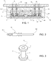
- Figure 1 shows a power module 12, wherein the electrical components (including any micro-electro-mechanical components) are connected to a printed circuit board through a solderless pressfit technique, according to a known solution.
- two dice are attached to a dissipating plate 2.
- the dice 1 may integrate electrical and/or electromechanical structures and have power and/or control functions, separately from each other or integrated in a same die.
- the dissipating plate 2 is formed by a DBC (Direct Bonded Copper) multilayer formed by a first and a second metal layer 2A, 2B and by an intermediate insulating layer 2C, for example of ceramic. At least one of the metal layers (here the first metal layer 2A) is shaped, so as to define reciprocally insulated conductive regions. Each die 1 is attached to a respective conductive region of the first metal layer 2A.
- DBC Direct Bonded Copper
- pin holders 3 are attached to respective conductive regions of the first metal layer 2A of the dissipating plate 2.
- Each pin holder 3 ( Figure 3 ) is formed by a tubular body 5, here of cylindrical shape, having an axial cavity 6 and provided with a pair of flanges 7 on its bases.
- the pin holders 3 are attached to the dissipating plate 2 through respective soldering regions 8.
- each soldering region 8 is arranged between one of the flanges 4 of the respective pin holder 3 and the dissipating plate 2. Soldering regions 8 are also arranged between the dice 1 and the respective conductive regions of the first metal layer 2A.
- Wires 9 are selectively soldered between pads (not visible) of the dice 1 and selective conductive regions of the first metal layer 2A to electrically connect the dice 1 to each other and to the outside, according to a desired electric diagram.
- connection to the outside is obtained through pins 10 fastened to the pin holders 3.
- the pins 10 have an elongated shape and may be shaped as shown in Figure 2 .
- the pins 10 are rod-shaped elements, of a length comprised between 13 and 15 mm and a square section (for example with a side of 0.64 mm). Furthermore, they may be provided with enlarged stop zones for blocking with respect to a connection support 11, described in detail hereinbelow.
- the pins 10 have a first end 10A and a second end 10B.
- the first end 10A of the pins 10 is preferably pointed and is force fitted into the axial cavity 6 of the respective pin holder 3 to obtain a press-fit.
- the second end 10B of the pins 10 is here transversely holed (as a keyhole, see in particular Figure 2 ).
- the second end 10B of the pins 10 is thus elastically flexible in transversal direction with respect to its length, thus allowing the pins 10 to be fixed to the connection support 11, as described hereinbelow.
- the dissipating plate 2 is fixed to a housing 13, for example of plastic.
- the housing 13 is formed by a side wall 13A and by a bottom wall 13B.
- the side wall 13A surrounds a chamber 15 and, on its edge opposite to the bottom wall 13B, has an inner peripheral notch 16 where the dissipating plate 2 is attached.
- the dissipating plate 2 is arranged so that the dice 1 and the pin holders 3 face the inside of the chamber 15 of the housing 13; in practice the dissipating plate 2 closes the chamber 15 on one side.
- a potting compound 17 may be provided inside the chamber for insulating and protecting the dice 1 and the electrical connections.
- the bottom wall 13B of the housing 13 has a plurality of holes 18, through which the pins 10 extend.
- connection support 11 is fixed to the housing 13 externally, to the bottom wall 13B thereof.
- the connection support 11 is made, for example, by a printed circuit board PCB and has, in turn, a plurality of through openings 19 aligned with the holes 18.
- the through openings 19 have conductive walls, for example have a surface metal coating (not shown), and are sized in such a way that the second end 10B of the pins 10 may be forced fitted and remain blocked into the through openings 19, due to its elasticity, with a press-fit coupling.
- connection support 11 In this manner, a good mechanical retention of the pins and a good electrical connection between the connection support 11 and the dice 1 are obtained without the need for soldering at the level of the connection support 11, as often required for automotive applications.
- the power module 12 described above is assembled by securing the dice 1 and the pin holders 3 to the dissipating plate 2; then inserting the pins 10 into the pin holders 3; fixing the dissipating plate 2 to the housing 13, after introducing the potting compound 17, and press-fitting the second ends 10B of the pins 10 into the connection support 11.
- fixing of the pin holders 3 is performed by soldering.
- a solder cream or paste is spread on the dissipating plate 2; the pin holders 3 are suitably placed by a manipulating machine; then a warm reflow process, followed by a wet washing step, is performed.
- solder cream used to temporarily hold the pin holders 3 in place is generally formed by an emulsion of a flux and soldering alloy beads which has an adhesive effect. During the reflow step, most of the flux is removed and the soldering alloy beads melt, soldering the pin holders 3 to the dissipating plate 2.
- the pin holders 3 are weakly held in place. Thus, it may occur that they move with respect to the desired position and, at the end of the process, are attached in the wrong position, displaced with respect to the desired one by a space of almost one millimeter. As a result, the respective pins 10 are also misplaced, creating problems to the final manufacturer for their fitting into the through openings 19.
- soldering process is expensive, since it requires two separate operations requiring a considerable amount of time and power to perform.
- further structures are provided to hold the pin holders 3 in place (in general metal fixtures), there is an increase in the quantity of metal. It means that, in case of furnace reflow, more heating energy is necessary, which leads to longer working time, more energy required, higher material costs and thus additional costs.
- the reflow process may also lead to the generation of thermomechanical stresses detrimental to the electronic components.
- US 2009/194884 discloses a pin blocking element for use in a power semiconductor module.
- the pin blocking element extends longitudinally and has flanges at its end.
- One of the flanges is soldered to a circuit carrier; the flanges have outer radii that may be chosen independently on one another.
- the aim of the present invention is to provide a solution to the problems highlighted hereinabove.
- a blocking element for connecting pins of semiconductor dice, a mounted plate for connection of electronic components, a power module and an assembling method are provided, as defined in the attached claims.
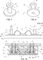
- Figures 7 and 8 show a pin holder 20 usable in a power module 50 shown in Figure 10 and similar to the power module of Figure 1 .
- the pin holder 20 is formed by a tubular body 21, in particular cylindrical, having an axial cavity 22, a first flange 23 at a first base and a second flange 24 at a second base.
- first flange 22 has a greater diameter with respect to the second flange 24.
- the first flange 23 may have an outer diameter comprised between 2.5 and 4 mm, in particular of 3-3.5 mm; and the second flange 24 may have an outer diameter comprised between 1.25 and 2.5 mm, in particular of 1.5-1.75 mm.
- the pin holder 20 is also, for example, of copper or bronze.
- the pin holder 20 of Figures 7 and 8 is fixed through High Power Ultrasonic Welding, HPUS, to a bearing plate 25, as shown in Figures 9 and 10 .
- Figure 9 shows a mounted plate 26 formed by a bearing plate 25 to which the pin holders 20 are fixed.
- the bearing plate 25 also bears dice 30, integrating electrical and/or electro-mechanical structures; in particular, the dice 30 may have power and/or control functions, integrated separately from each other or in a same die.
- the dice 30 and the pin holders 20 are attached, here each in a respective conductive region of the first metal layer 2A, through an ultrasonic technique, without using reflow processes, as described hereinbelow.
- the bearing plate 25 is formed by a DBC (Direct Bonded Copper) multilayer formed by a first and a second metal layer 25A, 25B and by an intermediate insulating layer 25C, for example of ceramic. At least one of the metal layers (here the first metal layer 25A), is shaped, so as to define conductive regions insulated from each other.
- DBC Direct Bonded Copper
- Wires 29 are selectively bonded between pads (not visible) of the dice 30 and respective regions of the first metal layer 25A.
- pins 31 have already been attached to the pin holders 20.
- the pins 31 may be exactly like the pins 10 of Figure 2 ; in particular they have an elongated shape having a first end 31A intended to be press-fitted into the axial cavity 22 of a respective pin holder 20 and a second end 31B that is deformable, intended to be press-fitted into a connection support 41 (see Figure 10 ) .
- the mounted plate 26 may be attached to the power module 50 of Figure 10 , comprising (similarly to the power module of Figure 1 ) a housing 33 formed by a side wall 33A and by a bottom wall 33B.
- the side wall 33A surrounds a chamber 35 and, on its edge opposite to the bottom wall 33B, has an internal peripheral notch 36 to which the dissipating plate 25 is attached.
- the dissipating plate 25 is arranged so that the dice 30 and the pin holders 20 face the inside of the chamber 35 of the housing 33 and, in practice, closes the chamber 35 on one side.
- a potting compound 37 may be provided inside the chamber for insulating and protecting the dice 30 and the electrical connections.
- the bottom wall 33B of the housing 33 has a plurality of holes 38 in which the pins 31 extend.
- the pins 31 are also press-fitted, at a second end thereof, into through openings 40 of the connection support 41, formed for example as a printed circuit board PCB, similarly to what previously described with reference to Figure 1 .
- the pin holders 20 and the dice 30 are attached to the bearing plate 25 through Ultra Power Ultrasound Welding, HPUS.
- the pin holders 20 may be picked up and placed on the bearing plate 25 through a transducer 60 shown in Figures 11-13 .
- the transducer 60 of Figures 11-13 has a gripping portion 61 that is hollow and has a gripping cavity 62 that is cylindrical and has a diameter comprised between the diameter of the first flange 23 and the diameter of the second flange 24 of the pin holders 20.
- the gripping portion 61 is coupled to vacuum generation means 64, capable of creating a depression inside the gripping cavity 62, and to welding ultrasonic energy generation means 65.
- the vacuum generation means 64 is activated and the transducer 60 picks up a pin holder 20, sucking it so that the second flange 24 thereof (smaller) and the tubular body 21 are sucked inside the gripping cavity 62 and only the first flange 23 abuts against the base of the gripping element 41 of the transducer 60 ( Figure 13 ). Then the transducer 60 places the pin holder 20 in a desired manner on the bearing plate 25 and welds it through the HPUS technique, following deactivation of the vacuum generation means 64 and activation of the welding ultrasonic energy generation means 65 (for example at a frequency comprised between 20 and 50 kHz).
- the transducer 60 presses the pin holder 20 against the bearing plate 25, applying ultrasonic energy (at high frequency).
- the transducer 60 may operate at room temperature, with a power lower than 1kW, applying a force comprised between 10 and 200 N for 0.1-1 seconds.
- the dice 30 may be welded with the same technique.
- the depression created in the gripping cavity 62 allows a die 30 to be held against the base of the transducer 60 and to be suitably placed on the bearing plate 25, before welding.
- the wires 29 are bonded to the bearing plate 25 and to the dice 30 through known techniques, for connecting the dice 30 to each other and/or to the pin holders 20.
- the pins 31 may each be press-fitted into a respective pin holder 20 and the steps described above may be performed to complete assembling of the power module 50.
- the pins 31 may also be placed in an accurate manner both in the pin holders 20 and in the connection support 41.
- the large surface of the first base 23 provides a wide attachment area, making it very stable even over time.
- the high-pressure ultrasound welding process further allows the reflow step and the successive washing step previously used to be eliminated, reducing assembling costs thanks to both the elimination of per se expensive steps and the reduction of the number of steps.
- thermomechanical stress on the system may be reduced, increasing the production yield.
- the dice 30 are electrically connected through wires 29, they may be made by packaged components connected through a surface mounting technique.
Landscapes
- Engineering & Computer Science (AREA)
- Manufacturing & Machinery (AREA)
- Microelectronics & Electronic Packaging (AREA)
- Coupling Device And Connection With Printed Circuit (AREA)
- Chemical & Material Sciences (AREA)
- Ceramic Engineering (AREA)
- Connections Effected By Soldering, Adhesion, Or Permanent Deformation (AREA)
- Multi-Conductor Connections (AREA)
- Lead Frames For Integrated Circuits (AREA)
- Connecting Device With Holders (AREA)
Abstract
Description
- The present invention relates to a blocking element for connecting pins of semiconductor dice, in particular for power modules for automotive applications, and to an assembling method. More particularly, the invention is applicable to electric propulsion vehicles.
- As known, the electric propulsion vehicles comprise control electronics of an electric motor. In particular, the control electronics associated with vehicles of this type comprises power modules and signal processing modules; furthermore, there are special connection structures, which require connecting pins of larger dimensions with respect to the electronic circuits used in other fields.
- For example,
Figure 1 shows apower module 12, wherein the electrical components (including any micro-electro-mechanical components) are connected to a printed circuit board through a solderless pressfit technique, according to a known solution. - In the embodiment shown in
Figure 1 , two dice, indicated with 1, are attached to adissipating plate 2. The dice 1 may integrate electrical and/or electromechanical structures and have power and/or control functions, separately from each other or integrated in a same die. - Here, the
dissipating plate 2 is formed by a DBC (Direct Bonded Copper) multilayer formed by a first and asecond metal layer layer 2C, for example of ceramic. At least one of the metal layers (here thefirst metal layer 2A) is shaped, so as to define reciprocally insulated conductive regions. Each die 1 is attached to a respective conductive region of thefirst metal layer 2A. - As also shown in
Figures 4-6 ,pin holders 3 are attached to respective conductive regions of thefirst metal layer 2A of thedissipating plate 2. Each pin holder 3 (Figure 3 ) is formed by atubular body 5, here of cylindrical shape, having anaxial cavity 6 and provided with a pair offlanges 7 on its bases. - With reference again to
Figures 1 ,4-6 , thepin holders 3 are attached to thedissipating plate 2 throughrespective soldering regions 8. - In particular, each soldering
region 8 is arranged between one of the flanges 4 of therespective pin holder 3 and thedissipating plate 2. Solderingregions 8 are also arranged between the dice 1 and the respective conductive regions of thefirst metal layer 2A. -
Wires 9 are selectively soldered between pads (not visible) of the dice 1 and selective conductive regions of thefirst metal layer 2A to electrically connect the dice 1 to each other and to the outside, according to a desired electric diagram. - In particular, the connection to the outside is obtained through
pins 10 fastened to thepin holders 3. - The
pins 10 have an elongated shape and may be shaped as shown inFigure 2 . In particular, here, thepins 10 are rod-shaped elements, of a length comprised between 13 and 15 mm and a square section (for example with a side of 0.64 mm). Furthermore, they may be provided with enlarged stop zones for blocking with respect to aconnection support 11, described in detail hereinbelow. - The
pins 10 have afirst end 10A and asecond end 10B. - The
first end 10A of thepins 10 is preferably pointed and is force fitted into theaxial cavity 6 of therespective pin holder 3 to obtain a press-fit. - The
second end 10B of thepins 10 is here transversely holed (as a keyhole, see in particularFigure 2 ). Thesecond end 10B of thepins 10 is thus elastically flexible in transversal direction with respect to its length, thus allowing thepins 10 to be fixed to theconnection support 11, as described hereinbelow. - The
dissipating plate 2 is fixed to ahousing 13, for example of plastic. Thehousing 13 is formed by aside wall 13A and by abottom wall 13B. Theside wall 13A surrounds achamber 15 and, on its edge opposite to thebottom wall 13B, has an innerperipheral notch 16 where thedissipating plate 2 is attached. In particular, thedissipating plate 2 is arranged so that the dice 1 and thepin holders 3 face the inside of thechamber 15 of thehousing 13; in practice thedissipating plate 2 closes thechamber 15 on one side. - A
potting compound 17 may be provided inside the chamber for insulating and protecting the dice 1 and the electrical connections. - The
bottom wall 13B of thehousing 13 has a plurality ofholes 18, through which thepins 10 extend. - The
connection support 11 is fixed to thehousing 13 externally, to thebottom wall 13B thereof. Theconnection support 11 is made, for example, by a printed circuit board PCB and has, in turn, a plurality of throughopenings 19 aligned with theholes 18. - The through
openings 19 have conductive walls, for example have a surface metal coating (not shown), and are sized in such a way that thesecond end 10B of thepins 10 may be forced fitted and remain blocked into the throughopenings 19, due to its elasticity, with a press-fit coupling. - In this manner, a good mechanical retention of the pins and a good electrical connection between the
connection support 11 and the dice 1 are obtained without the need for soldering at the level of theconnection support 11, as often required for automotive applications. - The
power module 12 described above is assembled by securing the dice 1 and thepin holders 3 to thedissipating plate 2; then inserting thepins 10 into thepin holders 3; fixing thedissipating plate 2 to thehousing 13, after introducing thepotting compound 17, and press-fitting thesecond ends 10B of thepins 10 into theconnection support 11. - In particular, fixing of the
pin holders 3 is performed by soldering. To this end, a solder cream or paste is spread on thedissipating plate 2; thepin holders 3 are suitably placed by a manipulating machine; then a warm reflow process, followed by a wet washing step, is performed. - The solder cream used to temporarily hold the
pin holders 3 in place is generally formed by an emulsion of a flux and soldering alloy beads which has an adhesive effect. During the reflow step, most of the flux is removed and the soldering alloy beads melt, soldering thepin holders 3 to thedissipating plate 2. - Therefore, in this step, before the soldering alloy beads are completely melted, the
pin holders 3 are weakly held in place. Thus, it may occur that they move with respect to the desired position and, at the end of the process, are attached in the wrong position, displaced with respect to the desired one by a space of almost one millimeter. As a result, therespective pins 10 are also misplaced, creating problems to the final manufacturer for their fitting into thethrough openings 19. - Furthermore, the soldering process is expensive, since it requires two separate operations requiring a considerable amount of time and power to perform. Furthermore, in case further structures are provided to hold the
pin holders 3 in place (in general metal fixtures), there is an increase in the quantity of metal. It means that, in case of furnace reflow, more heating energy is necessary, which leads to longer working time, more energy required, higher material costs and thus additional costs. - The reflow process may also lead to the generation of thermomechanical stresses detrimental to the electronic components.
-
US 2009/194884 discloses a pin blocking element for use in a power semiconductor module. The pin blocking element extends longitudinally and has flanges at its end. One of the flanges is soldered to a circuit carrier; the flanges have outer radii that may be chosen independently on one another. -
US 2019/189529 discloses ultrasonic welding methods for semiconductor modules. - The aim of the present invention is to provide a solution to the problems highlighted hereinabove.
- According to the present invention, a blocking element for connecting pins of semiconductor dice, a mounted plate for connection of electronic components, a power module and an assembling method are provided, as defined in the attached claims.
- For a better understanding of the present invention, an embodiment thereof is now described, purely by way of nonlimiting example, with reference to the attached drawings, wherein:
-
Figure 1 is a cross-section through a power module usable for automotive applications; -
Figure 2 is top plan view of a pin of the power module ofFigure 1 ; -
Figure 3 is a perspective view of a pin holder of the power module ofFigure 1 ; -
Figure 4 is a perspective view of a portion of the power module ofFigure 1 in an assembling step; -
Figure 5 is a cross-section through the detail ofFigure 4 ; -
Figure 6 is a perspective view of another portion of the power module ofFigure 1 in an assembling step successive toFigure 4 ; -
Figure 7 is a perspective top view of the present pin holder; -
Figure 8 is a perspective bottom view of the present pin holder; -
Figure 9 is a cross-section of a portion of a mounted plate to be assembled in a power module and including the pin holder ofFigures 7 and 8 ; -
Figure 10 is a cross-section through a power module including the mounted plate ofFigure 9 ; and -
Figures 11-13 show a transducer usable for welding the pin holder ofFigures 7 and 8 , respectively, in a perspective top view, in a perspective bottom view and while holding the present pin holder. -
Figures 7 and 8 show apin holder 20 usable in apower module 50 shown inFigure 10 and similar to the power module ofFigure 1 . - With reference to
Figures 7, 8 , thepin holder 20 is formed by atubular body 21, in particular cylindrical, having anaxial cavity 22, afirst flange 23 at a first base and asecond flange 24 at a second base. - In particular, the
first flange 22 has a greater diameter with respect to thesecond flange 24. - For example, for a
pin holder 20 having a height comprised between 3 and 7 mm, in particular of 3.5-5 mm, thefirst flange 23 may have an outer diameter comprised between 2.5 and 4 mm, in particular of 3-3.5 mm; and thesecond flange 24 may have an outer diameter comprised between 1.25 and 2.5 mm, in particular of 1.5-1.75 mm. - The
pin holder 20 is also, for example, of copper or bronze. - The
pin holder 20 ofFigures 7 and 8 is fixed through High Power Ultrasonic Welding, HPUS, to abearing plate 25, as shown inFigures 9 and 10 . -
Figure 9 shows amounted plate 26 formed by a bearingplate 25 to which thepin holders 20 are fixed. - The bearing
plate 25 also bearsdice 30, integrating electrical and/or electro-mechanical structures; in particular, thedice 30 may have power and/or control functions, integrated separately from each other or in a same die. Thedice 30 and thepin holders 20 are attached, here each in a respective conductive region of thefirst metal layer 2A, through an ultrasonic technique, without using reflow processes, as described hereinbelow. - The bearing
plate 25 is formed by a DBC (Direct Bonded Copper) multilayer formed by a first and asecond metal layer layer 25C, for example of ceramic. At least one of the metal layers (here thefirst metal layer 25A), is shaped, so as to define conductive regions insulated from each other. -
Wires 29 are selectively bonded between pads (not visible) of thedice 30 and respective regions of thefirst metal layer 25A. - In the mounted
plate 26 ofFigure 9 , pins 31 have already been attached to thepin holders 20. Thepins 31 may be exactly like thepins 10 ofFigure 2 ; in particular they have an elongated shape having a first end 31A intended to be press-fitted into theaxial cavity 22 of arespective pin holder 20 and a second end 31B that is deformable, intended to be press-fitted into a connection support 41 (seeFigure 10 ) . - The mounted
plate 26 may be attached to thepower module 50 ofFigure 10 , comprising (similarly to the power module ofFigure 1 ) ahousing 33 formed by aside wall 33A and by abottom wall 33B. Theside wall 33A surrounds achamber 35 and, on its edge opposite to thebottom wall 33B, has an internalperipheral notch 36 to which the dissipatingplate 25 is attached. The dissipatingplate 25 is arranged so that thedice 30 and thepin holders 20 face the inside of thechamber 35 of thehousing 33 and, in practice, closes thechamber 35 on one side. - A potting
compound 37 may be provided inside the chamber for insulating and protecting thedice 30 and the electrical connections. - The
bottom wall 33B of thehousing 33 has a plurality ofholes 38 in which thepins 31 extend. Thepins 31 are also press-fitted, at a second end thereof, into throughopenings 40 of theconnection support 41, formed for example as a printed circuit board PCB, similarly to what previously described with reference toFigure 1 . - As indicated above, the
pin holders 20 and thedice 30 are attached to the bearingplate 25 through Ultra Power Ultrasound Welding, HPUS. - In particular, the
pin holders 20 may be picked up and placed on the bearingplate 25 through atransducer 60 shown inFigures 11-13 . - Specifically, the
transducer 60 ofFigures 11-13 has a grippingportion 61 that is hollow and has agripping cavity 62 that is cylindrical and has a diameter comprised between the diameter of thefirst flange 23 and the diameter of thesecond flange 24 of thepin holders 20. - In an only schematically shown manner, the gripping
portion 61 is coupled to vacuum generation means 64, capable of creating a depression inside the grippingcavity 62, and to welding ultrasonic energy generation means 65. - Then, during the assembling step, the vacuum generation means 64 is activated and the
transducer 60 picks up apin holder 20, sucking it so that thesecond flange 24 thereof (smaller) and thetubular body 21 are sucked inside the grippingcavity 62 and only thefirst flange 23 abuts against the base of thegripping element 41 of the transducer 60 (Figure 13 ). Then thetransducer 60 places thepin holder 20 in a desired manner on the bearingplate 25 and welds it through the HPUS technique, following deactivation of the vacuum generation means 64 and activation of the welding ultrasonic energy generation means 65 (for example at a frequency comprised between 20 and 50 kHz). - In practice, the
transducer 60 presses thepin holder 20 against the bearingplate 25, applying ultrasonic energy (at high frequency). - For example, the
transducer 60 may operate at room temperature, with a power lower than 1kW, applying a force comprised between 10 and 200 N for 0.1-1 seconds. - The
dice 30 may be welded with the same technique. In particular, in this case, the depression created in thegripping cavity 62 allows a die 30 to be held against the base of thetransducer 60 and to be suitably placed on the bearingplate 25, before welding. - If the components have wire connections of the type shown in
Figures 9 and 10 , thewires 29 are bonded to the bearingplate 25 and to thedice 30 through known techniques, for connecting thedice 30 to each other and/or to thepin holders 20. - Then, the
pins 31 may each be press-fitted into arespective pin holder 20 and the steps described above may be performed to complete assembling of thepower module 50. - In this manner, a very stable, resistant and accurate welding of the pin holders 20 (and of the dice 30) is obtained, with lower costs with respect to the known solution.
- In fact, due to the increased size of the
first base 23 of thepin holders 20, they may be picked up, held and accurately placed on the bearingplate 25. In this manner, a bonding accuracy of ±0.05 mm may be achieved, with a considerable improvement with respect to the current techniques. - As a result the
pins 31 may also be placed in an accurate manner both in thepin holders 20 and in theconnection support 41. - Furthermore, the large surface of the
first base 23 provides a wide attachment area, making it very stable even over time. - The high-pressure ultrasound welding process further allows the reflow step and the successive washing step previously used to be eliminated, reducing assembling costs thanks to both the elimination of per se expensive steps and the reduction of the number of steps.
- Since the welding occurs at room temperature, thermal treatments may be eliminated, and thus any thermomechanical stress on the system may be reduced, increasing the production yield.
- Finally, it is clear that modifications and variations may be made to the blocking element for connecting pins, to the mounted plate, to the power module and to the assembling process described and illustrated herein without thereby departing from the protective scope of the present invention, as defined in the attached claims.
- For example, although in the figures the
dice 30 are electrically connected throughwires 29, they may be made by packaged components connected through a surface mounting technique.
Claims (15)
- A pin blocking element (20) for connecting an electronic, micro-mechanical and/or micro-electro-mechanical component, in particular for controlling the propulsion of an electric vehicle, comprising a holed body (21) having a first end, a second end and an axial cavity (22) configured for fittingly accommodating a connecting pin (31), wherein a first flange (23) projects transversely from the holed body (21) at the first end, a second flange (24) projects transversely from the holed body (21) at the second end, the first flange (23) has a larger area than the second flange (24) and is configured to be ultrasonically welded to a conductive bearing plate (25).
- The pin blocking element according to claim 1, wherein the holed body (21) is tubular, for example cylindrical.
- The pin blocking element according to claim 1 or 2, wherein the holed body (21) has a height comprised between 3 and 7 mm, the first flange (23) may have an outer diameter comprised between 2.5 and 4 mm, in particular of 3-3.5 mm; and the second flange (24) may have an outer diameter comprised between 1.25 and 2.5 mm, in particular of 1.5-1.75 mm.
- A connection mounted plate of electronic, micro-mechanical and/or micro-electro-mechanical components, comprising a bearing plate (25) having at least one first and one second conductive region (25A) that are reciprocally insulated, the first conductive region bearing a semiconductor die (30) and the second conductive region bearing a pin blocking element (20) according to any of the preceding claims,
characterized in that the first flange of the pin blocking element (20) and the semiconductor die (30) are welded to the bearing plate (25) without interposed material. - The connection mounted plate according to the preceding claim, wherein the bearing plate (25) is a DBC support comprising a first and a second conductive layer (25A), (25B) and an intermediate insulating layer (25C).
- The connection mounted plate according to claim 4 or 5, further comprising at least one connecting pin (31) fitted into the pin blocking element (20), the connecting pin (31) having a first end (10A) fitted in the axial cavity (22) of the pin blocking element (20) and a deformable second end (10B) provided with a keyhole.
- The connection mounted plate according to any of claims 4-6, wherein the electronic, micro-mechanical and/or micro-electro-mechanical components belong to a propulsion control circuit of an electric vehicle.
- A power module, comprising a housing (33) having a bottom wall (33B) and a side wall (33A) defining a chamber, wherein the side wall (33A) has a coupling edge for coupling with the connection mounted plate (25) according to any of claims 4-6 and the bottom wall (33B) has at least one through hole (38) traversed by the connecting pin (31), the power module (50) further comprising a connection support (41) attached to the housing (33) and facing the bottom wall (33B), the connection support (41) having at least one through opening (40) coupled through press-fit to the second end of the connecting pin (20).
- The power module according to the preceding claim, wherein the connection support (41) is a printed circuit.
- An assembling method comprising:providing a bearing plate (25) having at least one first and one second conductive region (25A) that are reciprocally insulated;attaching a semiconductor die (30) to the first conductive region (25A) of the bearing plate (25);attaching a pin blocking element (20) to the second conductive region (25A), wherein the pin blocking element (20) has a holed body (21) provided with a first flange (23) at a first end, a second flange (24) at a second end and the first flange (23) has a larger area than the second flange (24) ;wherein attaching a pin blocking element (20) comprises placing the pin blocking element with the first flange (23) in contact with the second conductive region (25A),characterized in that attaching a pin blocking element (20) further comprises ultrasonically welding using an High Power Ultrasonic - HPUS welding technique.
- The assembling method according to the preceding claim, wherein the bearing plate (25) is a Direct Bonded Copper - DBC support.
- The assembling method according to claim 10 or 11, further comprising fixing one end of a rod-shaped connecting pin (31) to the holed body (21) through interference fit.
- The assembling method according to any of the claims 10-12, wherein the holed body (21) has a height comprised between 3 and 7 mm, the first flange (23) may have an outer diameter comprised between 2.5 and 4 mm, in particular of 3-3.5 mm; and the second flange (24) may have an outer diameter comprised between 1.25 and 2.5 mm, in particular of 1.5-1.75 mm.
- The assembling method according to any of claims 10-13, wherein ultrasonically welding comprises:sucking the pin blocking element (20) in a gripping cavity (62) of a transducer (60) so that the second flange (24) and the holed body (21) enter the gripping cavity (62);placing the second flange (24) of the pin blocking element (20) on the second conductive region (25A) of the bearing plate (25); andgenerating ultrasound.
- The assembling method according to the preceding claim, wherein generating ultrasound comprises applying a power lower than 1 kW, a force comprised between 10 and 200 N for 0.1-1 seconds at room temperature.
Applications Claiming Priority (1)
| Application Number | Priority Date | Filing Date | Title |
|---|---|---|---|
| IT102020000023641A IT202000023641A1 (en) | 2020-10-07 | 2020-10-07 | ELEMENT FOR CLAMPING PINS OF CONNECTION OF SEMICONDUCTRIC LEADS, PARTICULARLY FOR POWER MODULES FOR AUTOMOTIVE APPLICATIONS, AND METHOD OF ASSEMBLY |
Publications (3)
| Publication Number | Publication Date |
|---|---|
| EP3982401A1 true EP3982401A1 (en) | 2022-04-13 |
| EP3982401C0 EP3982401C0 (en) | 2024-12-25 |
| EP3982401B1 EP3982401B1 (en) | 2024-12-25 |
Family
ID=73793748
Family Applications (1)
| Application Number | Title | Priority Date | Filing Date |
|---|---|---|---|
| EP21201233.0A Active EP3982401B1 (en) | 2020-10-07 | 2021-10-06 | Plate for a power module with semiconductor die and pin holder welded thereto |
Country Status (4)
| Country | Link |
|---|---|
| US (2) | US12094806B2 (en) |
| EP (1) | EP3982401B1 (en) |
| CN (2) | CN216905460U (en) |
| IT (1) | IT202000023641A1 (en) |
Cited By (3)
| Publication number | Priority date | Publication date | Assignee | Title |
|---|---|---|---|---|
| EP4312259A1 (en) * | 2022-07-28 | 2024-01-31 | Infineon Technologies AG | Press-fit connector and receptacle |
| US20240091876A1 (en) * | 2020-06-03 | 2024-03-21 | Kulicke And Soffa Industries, Inc. | Ultrasonic welding systems, methods of using the same, and related workpieces including welded conductive pins |
| WO2026111757A1 (en) * | 2024-11-22 | 2026-05-28 | Semiconductor Components Industries, Llc | Direct bonded metal (dbm) and connection technology |
Families Citing this family (11)
| Publication number | Priority date | Publication date | Assignee | Title |
|---|---|---|---|---|
| IT201800020275A1 (en) * | 2018-12-20 | 2020-06-20 | Amx Automatrix S R L | SINTERING PRESS FOR SINTERING ELECTRONIC COMPONENTS ON A SUBSTRATE |
| IT202000023641A1 (en) * | 2020-10-07 | 2022-04-07 | St Microelectronics Srl | ELEMENT FOR CLAMPING PINS OF CONNECTION OF SEMICONDUCTRIC LEADS, PARTICULARLY FOR POWER MODULES FOR AUTOMOTIVE APPLICATIONS, AND METHOD OF ASSEMBLY |
| US20230307314A1 (en) * | 2022-03-24 | 2023-09-28 | Texas Instruments Incorporated | Direct bond copper substrate with metal filled ceramic substrate indentations |
| EP4276888A1 (en) * | 2022-05-09 | 2023-11-15 | Infineon Technologies AG | Method for producing a power semiconductor module |
| DE102023108539A1 (en) * | 2023-04-04 | 2024-10-10 | Danfoss Silicon Power Gmbh | SEMICONDUCTOR POWER MODULE AND METHOD FOR PRODUCING SUCH A POWER MODULE |
| TWI851424B (en) * | 2023-09-20 | 2024-08-01 | 朋程科技股份有限公司 | Semiconductor module and manufacturing method thereof |
| WO2025142441A1 (en) * | 2023-12-28 | 2025-07-03 | ローム株式会社 | Semiconductor device and method for manufacturing semiconductor device |
| US20250379197A1 (en) * | 2024-06-07 | 2025-12-11 | Infineon Technologies Ag | Low Profile Power Module |
| DE102025104867A1 (en) * | 2025-02-10 | 2026-08-13 | Volkswagen Aktiengesellschaft | Component arrangement for an electronic system and a method for providing a component arrangement for an electronic system |
| DE102025105521A1 (en) * | 2025-02-14 | 2026-08-20 | Infineon Technologies Ag | Rivet-shaped element for use in a semiconductor module arrangement, method for producing a rivet-shaped element and method for joining a rivet-shaped element to a substrate |
| DE102025112577B3 (en) * | 2025-03-31 | 2026-06-25 | Volkswagen Aktiengesellschaft | Power electronic component |
Citations (5)
| Publication number | Priority date | Publication date | Assignee | Title |
|---|---|---|---|---|
| US20090194884A1 (en) | 2008-01-23 | 2009-08-06 | Infineon Technologies Ag | Power semiconductor module including a contact element |
| JP2015179646A (en) * | 2014-03-20 | 2015-10-08 | 富士電機株式会社 | Pin insertion device and pin insertion failure determination method |
| DE102014211698A1 (en) * | 2014-06-18 | 2015-12-24 | Robert Bosch Gmbh | Electronic module with a contact sleeve |
| US20160380366A1 (en) * | 2015-06-25 | 2016-12-29 | Fuji Electric Co., Ltd. | Semiconductor device |
| US20190189529A1 (en) | 2017-12-19 | 2019-06-20 | Fuji Electric Co., Ltd. | Semiconductor module and semiconductor module manufacturing method |
Family Cites Families (8)
| Publication number | Priority date | Publication date | Assignee | Title |
|---|---|---|---|---|
| JP2007319876A (en) * | 2006-05-30 | 2007-12-13 | Toshiba Corp | Ultrasonic bonding apparatus and semiconductor device manufacturing method |
| US8563364B2 (en) * | 2011-09-29 | 2013-10-22 | Infineon Technologies Ag | Method for producing a power semiconductor arrangement |
| US20130175704A1 (en) * | 2012-01-05 | 2013-07-11 | Ixys Corporation | Discrete power transistor package having solderless dbc to leadframe attach |
| US20140167237A1 (en) * | 2012-12-14 | 2014-06-19 | Samsung Electro-Mechanics Co., Ltd. | Power module package |
| EP3627978B1 (en) * | 2018-09-19 | 2026-01-14 | Infineon Technologies AG | Power semiconductor module arrangement and housing for a power semiconductor arrangement |
| DE102018128097B4 (en) * | 2018-11-09 | 2022-08-11 | Infineon Technologies Ag | SEMICONDUCTOR POWER MODULE AND METHOD OF MANUFACTURING SEMICONDUCTOR POWER MODULE |
| JP7293936B2 (en) * | 2019-07-19 | 2023-06-20 | 富士電機株式会社 | Semiconductor device and method for manufacturing semiconductor device |
| IT202000023641A1 (en) * | 2020-10-07 | 2022-04-07 | St Microelectronics Srl | ELEMENT FOR CLAMPING PINS OF CONNECTION OF SEMICONDUCTRIC LEADS, PARTICULARLY FOR POWER MODULES FOR AUTOMOTIVE APPLICATIONS, AND METHOD OF ASSEMBLY |
-
2020
- 2020-10-07 IT IT102020000023641A patent/IT202000023641A1/en unknown
-
2021
- 2021-09-30 US US17/491,082 patent/US12094806B2/en active Active
- 2021-10-06 EP EP21201233.0A patent/EP3982401B1/en active Active
- 2021-10-08 CN CN202122417339.XU patent/CN216905460U/en active Active
- 2021-10-08 CN CN202111171089.4A patent/CN114302553A/en active Pending
-
2024
- 2024-09-10 US US18/830,402 patent/US20240429132A1/en active Pending
Patent Citations (5)
| Publication number | Priority date | Publication date | Assignee | Title |
|---|---|---|---|---|
| US20090194884A1 (en) | 2008-01-23 | 2009-08-06 | Infineon Technologies Ag | Power semiconductor module including a contact element |
| JP2015179646A (en) * | 2014-03-20 | 2015-10-08 | 富士電機株式会社 | Pin insertion device and pin insertion failure determination method |
| DE102014211698A1 (en) * | 2014-06-18 | 2015-12-24 | Robert Bosch Gmbh | Electronic module with a contact sleeve |
| US20160380366A1 (en) * | 2015-06-25 | 2016-12-29 | Fuji Electric Co., Ltd. | Semiconductor device |
| US20190189529A1 (en) | 2017-12-19 | 2019-06-20 | Fuji Electric Co., Ltd. | Semiconductor module and semiconductor module manufacturing method |
Cited By (5)
| Publication number | Priority date | Publication date | Assignee | Title |
|---|---|---|---|---|
| US20240091876A1 (en) * | 2020-06-03 | 2024-03-21 | Kulicke And Soffa Industries, Inc. | Ultrasonic welding systems, methods of using the same, and related workpieces including welded conductive pins |
| US12070814B2 (en) * | 2020-06-03 | 2024-08-27 | Kulicke And Soffa Industries, Inc. | Ultrasonic welding systems, methods of using the same, and related workpieces including welded conductive pins |
| EP4312259A1 (en) * | 2022-07-28 | 2024-01-31 | Infineon Technologies AG | Press-fit connector and receptacle |
| US12689140B2 (en) | 2022-07-28 | 2026-07-21 | Infineon Technologies Ag | Press-fit connector and receptacle |
| WO2026111757A1 (en) * | 2024-11-22 | 2026-05-28 | Semiconductor Components Industries, Llc | Direct bonded metal (dbm) and connection technology |
Also Published As
| Publication number | Publication date |
|---|---|
| EP3982401C0 (en) | 2024-12-25 |
| CN114302553A (en) | 2022-04-08 |
| US20240429132A1 (en) | 2024-12-26 |
| IT202000023641A1 (en) | 2022-04-07 |
| EP3982401B1 (en) | 2024-12-25 |
| US12094806B2 (en) | 2024-09-17 |
| CN216905460U (en) | 2022-07-05 |
| US20220108939A1 (en) | 2022-04-07 |
Similar Documents
| Publication | Publication Date | Title |
|---|---|---|
| EP3982401B1 (en) | Plate for a power module with semiconductor die and pin holder welded thereto | |
| JP4607995B2 (en) | Power semiconductor device | |
| TWI722362B (en) | Press-fit power module and related methods | |
| EP1868244B1 (en) | Semiconductor device | |
| CN101577262A (en) | Power semiconductor module system | |
| CN114402702B (en) | Power electronic component, method for producing a power electronic component, motor vehicle | |
| JP2014053630A (en) | Connection method to printed circuit not using soldering of electric drive unit | |
| US6401542B1 (en) | Pressure sensing semiconductor device comprising a semiconductor chip which has a diaphragm formed with piezoresistance | |
| JP2005051239A (en) | Reconnectable chip interface and chip package | |
| CN118053835A (en) | Electrical connector with bending portion and opening | |
| WO2024249311A1 (en) | Power module package with molded via and dual side press-fit pin | |
| KR20160009033A (en) | Contacting part for a drive module, drive module, and method for producing a contacting part | |
| WO2001018553A1 (en) | Conductive contact | |
| JP2005150226A (en) | Optical module for high-frequency signal transmission and manufacturing method thereof | |
| JP2002009217A (en) | Resin-sealed semiconductor device | |
| JP5528584B2 (en) | Device comprising an electrical and / or electronic module and a circuit support | |
| CN115274472A (en) | Method of manufacturing an electronic device and corresponding electronic device | |
| EP0312607A1 (en) | Power circuit board and manufacturing method | |
| US10559912B2 (en) | Method for producing and electrical assembly | |
| CN119422232A (en) | Power module package with molded through-hole and double-sided press-fit pins | |
| CN117790425A (en) | Isolated power packaging with flexible connections | |
| US7527535B2 (en) | System for electrical contacting | |
| JP3865243B2 (en) | Ceramic package for electronic parts and electronic device | |
| JP2014150128A (en) | Electronic device | |
| US20250273580A1 (en) | Power module and method for producing a power module |
Legal Events
| Date | Code | Title | Description |
|---|---|---|---|
| PUAI | Public reference made under article 153(3) epc to a published international application that has entered the european phase |
Free format text: ORIGINAL CODE: 0009012 |
|
| STAA | Information on the status of an ep patent application or granted ep patent |
Free format text: STATUS: THE APPLICATION HAS BEEN PUBLISHED |
|
| AK | Designated contracting states |
Kind code of ref document: A1 Designated state(s): AL AT BE BG CH CY CZ DE DK EE ES FI FR GB GR HR HU IE IS IT LI LT LU LV MC MK MT NL NO PL PT RO RS SE SI SK SM TR |
|
| STAA | Information on the status of an ep patent application or granted ep patent |
Free format text: STATUS: REQUEST FOR EXAMINATION WAS MADE |
|
| 17P | Request for examination filed |
Effective date: 20221010 |
|
| RBV | Designated contracting states (corrected) |
Designated state(s): AL AT BE BG CH CY CZ DE DK EE ES FI FR GB GR HR HU IE IS IT LI LT LU LV MC MK MT NL NO PL PT RO RS SE SI SK SM TR |
|
| GRAP | Despatch of communication of intention to grant a patent |
Free format text: ORIGINAL CODE: EPIDOSNIGR1 |
|
| STAA | Information on the status of an ep patent application or granted ep patent |
Free format text: STATUS: GRANT OF PATENT IS INTENDED |
|
| RIC1 | Information provided on ipc code assigned before grant |
Ipc: H05K 3/32 20060101ALN20240423BHEP Ipc: H01L 23/24 20060101ALN20240423BHEP Ipc: H01L 25/07 20060101ALN20240423BHEP Ipc: H01L 23/373 20060101ALI20240423BHEP Ipc: H05K 3/40 20060101ALI20240423BHEP Ipc: H01L 23/498 20060101ALI20240423BHEP Ipc: H01L 23/053 20060101AFI20240423BHEP |
|
| INTG | Intention to grant announced |
Effective date: 20240508 |
|
| GRAJ | Information related to disapproval of communication of intention to grant by the applicant or resumption of examination proceedings by the epo deleted |
Free format text: ORIGINAL CODE: EPIDOSDIGR1 |
|
| STAA | Information on the status of an ep patent application or granted ep patent |
Free format text: STATUS: REQUEST FOR EXAMINATION WAS MADE |
|
| GRAP | Despatch of communication of intention to grant a patent |
Free format text: ORIGINAL CODE: EPIDOSNIGR1 |
|
| STAA | Information on the status of an ep patent application or granted ep patent |
Free format text: STATUS: GRANT OF PATENT IS INTENDED |
|
| INTC | Intention to grant announced (deleted) | ||
| RIC1 | Information provided on ipc code assigned before grant |
Ipc: H05K 3/32 20060101ALN20240904BHEP Ipc: H01L 23/24 20060101ALN20240904BHEP Ipc: H01L 25/07 20060101ALN20240904BHEP Ipc: H01L 23/373 20060101ALI20240904BHEP Ipc: H05K 3/40 20060101ALI20240904BHEP Ipc: H01L 23/498 20060101ALI20240904BHEP Ipc: H01L 23/053 20060101AFI20240904BHEP |
|
| INTG | Intention to grant announced |
Effective date: 20240912 |
|
| GRAS | Grant fee paid |
Free format text: ORIGINAL CODE: EPIDOSNIGR3 |
|
| GRAA | (expected) grant |
Free format text: ORIGINAL CODE: 0009210 |
|
| STAA | Information on the status of an ep patent application or granted ep patent |
Free format text: STATUS: THE PATENT HAS BEEN GRANTED |
|
| AK | Designated contracting states |
Kind code of ref document: B1 Designated state(s): AL AT BE BG CH CY CZ DE DK EE ES FI FR GB GR HR HU IE IS IT LI LT LU LV MC MK MT NL NO PL PT RO RS SE SI SK SM TR |
|
| REG | Reference to a national code |
Ref country code: GB Ref legal event code: FG4D |
|
| REG | Reference to a national code |
Ref country code: CH Ref legal event code: EP |
|
| REG | Reference to a national code |
Ref country code: DE Ref legal event code: R096 Ref document number: 602021023812 Country of ref document: DE |
|
| REG | Reference to a national code |
Ref country code: IE Ref legal event code: FG4D |
|
| U01 | Request for unitary effect filed |
Effective date: 20241225 |
|
| U07 | Unitary effect registered |
Designated state(s): AT BE BG DE DK EE FI FR IT LT LU LV MT NL PT RO SE SI Effective date: 20250109 |
|
| PG25 | Lapsed in a contracting state [announced via postgrant information from national office to epo] |
Ref country code: HR Free format text: LAPSE BECAUSE OF FAILURE TO SUBMIT A TRANSLATION OF THE DESCRIPTION OR TO PAY THE FEE WITHIN THE PRESCRIBED TIME-LIMIT Effective date: 20241225 |
|
| PG25 | Lapsed in a contracting state [announced via postgrant information from national office to epo] |
Ref country code: NO Free format text: LAPSE BECAUSE OF FAILURE TO SUBMIT A TRANSLATION OF THE DESCRIPTION OR TO PAY THE FEE WITHIN THE PRESCRIBED TIME-LIMIT Effective date: 20250325 |
|
| PG25 | Lapsed in a contracting state [announced via postgrant information from national office to epo] |
Ref country code: GR Free format text: LAPSE BECAUSE OF FAILURE TO SUBMIT A TRANSLATION OF THE DESCRIPTION OR TO PAY THE FEE WITHIN THE PRESCRIBED TIME-LIMIT Effective date: 20250326 |
|
| PG25 | Lapsed in a contracting state [announced via postgrant information from national office to epo] |
Ref country code: RS Free format text: LAPSE BECAUSE OF FAILURE TO SUBMIT A TRANSLATION OF THE DESCRIPTION OR TO PAY THE FEE WITHIN THE PRESCRIBED TIME-LIMIT Effective date: 20250325 |
|
| PG25 | Lapsed in a contracting state [announced via postgrant information from national office to epo] |
Ref country code: SM Free format text: LAPSE BECAUSE OF FAILURE TO SUBMIT A TRANSLATION OF THE DESCRIPTION OR TO PAY THE FEE WITHIN THE PRESCRIBED TIME-LIMIT Effective date: 20241225 |
|
| PG25 | Lapsed in a contracting state [announced via postgrant information from national office to epo] |
Ref country code: PL Free format text: LAPSE BECAUSE OF FAILURE TO SUBMIT A TRANSLATION OF THE DESCRIPTION OR TO PAY THE FEE WITHIN THE PRESCRIBED TIME-LIMIT Effective date: 20241225 |
|
| PG25 | Lapsed in a contracting state [announced via postgrant information from national office to epo] |
Ref country code: ES Free format text: LAPSE BECAUSE OF FAILURE TO SUBMIT A TRANSLATION OF THE DESCRIPTION OR TO PAY THE FEE WITHIN THE PRESCRIBED TIME-LIMIT Effective date: 20241225 |
|
| PG25 | Lapsed in a contracting state [announced via postgrant information from national office to epo] |
Ref country code: IS Free format text: LAPSE BECAUSE OF FAILURE TO SUBMIT A TRANSLATION OF THE DESCRIPTION OR TO PAY THE FEE WITHIN THE PRESCRIBED TIME-LIMIT Effective date: 20250425 |
|
| PG25 | Lapsed in a contracting state [announced via postgrant information from national office to epo] |
Ref country code: SK Free format text: LAPSE BECAUSE OF FAILURE TO SUBMIT A TRANSLATION OF THE DESCRIPTION OR TO PAY THE FEE WITHIN THE PRESCRIBED TIME-LIMIT Effective date: 20241225 |
|
| PG25 | Lapsed in a contracting state [announced via postgrant information from national office to epo] |
Ref country code: CZ Free format text: LAPSE BECAUSE OF FAILURE TO SUBMIT A TRANSLATION OF THE DESCRIPTION OR TO PAY THE FEE WITHIN THE PRESCRIBED TIME-LIMIT Effective date: 20241225 |
|
| U20 | Renewal fee for the european patent with unitary effect paid |
Year of fee payment: 5 Effective date: 20250923 |
|
| PLBE | No opposition filed within time limit |
Free format text: ORIGINAL CODE: 0009261 |
|
| STAA | Information on the status of an ep patent application or granted ep patent |
Free format text: STATUS: NO OPPOSITION FILED WITHIN TIME LIMIT |
|
| REG | Reference to a national code |
Ref country code: CH Ref legal event code: L10 Free format text: ST27 STATUS EVENT CODE: U-0-0-L10-L00 (AS PROVIDED BY THE NATIONAL OFFICE) Effective date: 20251105 |
|
| 26N | No opposition filed |
Effective date: 20250926 |
|
| REG | Reference to a national code |
Ref country code: CH Ref legal event code: H13 Free format text: ST27 STATUS EVENT CODE: U-0-0-H10-H13 (AS PROVIDED BY THE NATIONAL OFFICE) Effective date: 20260527 |
|
| GBPC | Gb: european patent ceased through non-payment of renewal fee |
Effective date: 20251006 |
|
| PG25 | Lapsed in a contracting state [announced via postgrant information from national office to epo] |
Ref country code: MC Free format text: LAPSE BECAUSE OF FAILURE TO SUBMIT A TRANSLATION OF THE DESCRIPTION OR TO PAY THE FEE WITHIN THE PRESCRIBED TIME-LIMIT Effective date: 20241225 |
|
| PG25 | Lapsed in a contracting state [announced via postgrant information from national office to epo] |
Ref country code: GB Free format text: LAPSE BECAUSE OF NON-PAYMENT OF DUE FEES Effective date: 20251006 |
|
| PG25 | Lapsed in a contracting state [announced via postgrant information from national office to epo] |
Ref country code: CH Free format text: LAPSE BECAUSE OF NON-PAYMENT OF DUE FEES Effective date: 20251031 |