EP3980997B1 - Use of error correction codes to prevent errors in neighboring storage - Google Patents
Use of error correction codes to prevent errors in neighboring storage Download PDFInfo
- Publication number
- EP3980997B1 EP3980997B1 EP20731728.0A EP20731728A EP3980997B1 EP 3980997 B1 EP3980997 B1 EP 3980997B1 EP 20731728 A EP20731728 A EP 20731728A EP 3980997 B1 EP3980997 B1 EP 3980997B1
- Authority
- EP
- European Patent Office
- Prior art keywords
- data
- value
- probability
- storage device
- data storage
- Prior art date
- Legal status (The legal status is an assumption and is not a legal conclusion. Google has not performed a legal analysis and makes no representation as to the accuracy of the status listed.)
- Active
Links
Images

Classifications
-
- G—PHYSICS
- G06—COMPUTING OR CALCULATING; COUNTING
- G06F—ELECTRIC DIGITAL DATA PROCESSING
- G06F11/00—Error detection; Error correction; Monitoring
- G06F11/07—Responding to the occurrence of a fault, e.g. fault tolerance
- G06F11/08—Error detection or correction by redundancy in data representation, e.g. by using checking codes
- G06F11/10—Adding special bits or symbols to the coded information, e.g. parity check, casting out 9's or 11's
- G06F11/1076—Parity data used in redundant arrays of independent storages, e.g. in RAID systems
-
- G—PHYSICS
- G11—INFORMATION STORAGE
- G11C—STATIC STORES
- G11C11/00—Digital stores characterised by the use of particular electric or magnetic storage elements; Storage elements therefor
- G11C11/02—Digital stores characterised by the use of particular electric or magnetic storage elements; Storage elements therefor using magnetic elements
- G11C11/16—Digital stores characterised by the use of particular electric or magnetic storage elements; Storage elements therefor using magnetic elements using elements in which the storage effect is based on magnetic spin effect
- G11C11/165—Auxiliary circuits
- G11C11/1675—Writing or programming circuits or methods
-
- G—PHYSICS
- G06—COMPUTING OR CALCULATING; COUNTING
- G06F—ELECTRIC DIGITAL DATA PROCESSING
- G06F11/00—Error detection; Error correction; Monitoring
- G06F11/07—Responding to the occurrence of a fault, e.g. fault tolerance
- G06F11/08—Error detection or correction by redundancy in data representation, e.g. by using checking codes
- G06F11/10—Adding special bits or symbols to the coded information, e.g. parity check, casting out 9's or 11's
- G06F11/1008—Adding special bits or symbols to the coded information, e.g. parity check, casting out 9's or 11's in individual solid state devices
- G06F11/1048—Adding special bits or symbols to the coded information, e.g. parity check, casting out 9's or 11's in individual solid state devices using arrangements adapted for a specific error detection or correction feature
-
- G—PHYSICS
- G06—COMPUTING OR CALCULATING; COUNTING
- G06F—ELECTRIC DIGITAL DATA PROCESSING
- G06F3/00—Input arrangements for transferring data to be processed into a form capable of being handled by the computer; Output arrangements for transferring data from processing unit to output unit, e.g. interface arrangements
- G06F3/06—Digital input from, or digital output to, record carriers, e.g. RAID, emulated record carriers or networked record carriers
- G06F3/0601—Interfaces specially adapted for storage systems
- G06F3/0602—Interfaces specially adapted for storage systems specifically adapted to achieve a particular effect
- G06F3/0604—Improving or facilitating administration, e.g. storage management
-
- G—PHYSICS
- G06—COMPUTING OR CALCULATING; COUNTING
- G06F—ELECTRIC DIGITAL DATA PROCESSING
- G06F3/00—Input arrangements for transferring data to be processed into a form capable of being handled by the computer; Output arrangements for transferring data from processing unit to output unit, e.g. interface arrangements
- G06F3/06—Digital input from, or digital output to, record carriers, e.g. RAID, emulated record carriers or networked record carriers
- G06F3/0601—Interfaces specially adapted for storage systems
- G06F3/0628—Interfaces specially adapted for storage systems making use of a particular technique
- G06F3/0655—Vertical data movement, i.e. input-output transfer; data movement between one or more hosts and one or more storage devices
- G06F3/0659—Command handling arrangements, e.g. command buffers, queues, command scheduling
-
- G—PHYSICS
- G06—COMPUTING OR CALCULATING; COUNTING
- G06F—ELECTRIC DIGITAL DATA PROCESSING
- G06F3/00—Input arrangements for transferring data to be processed into a form capable of being handled by the computer; Output arrangements for transferring data from processing unit to output unit, e.g. interface arrangements
- G06F3/06—Digital input from, or digital output to, record carriers, e.g. RAID, emulated record carriers or networked record carriers
- G06F3/0601—Interfaces specially adapted for storage systems
- G06F3/0668—Interfaces specially adapted for storage systems adopting a particular infrastructure
- G06F3/0671—In-line storage system
- G06F3/0673—Single storage device
-
- G—PHYSICS
- G11—INFORMATION STORAGE
- G11B—INFORMATION STORAGE BASED ON RELATIVE MOVEMENT BETWEEN RECORD CARRIER AND TRANSDUCER
- G11B5/00—Recording by magnetisation or demagnetisation of a record carrier; Reproducing by magnetic means; Record carriers therefor
- G11B5/012—Recording on, or reproducing or erasing from, magnetic disks
-
- G—PHYSICS
- G11—INFORMATION STORAGE
- G11C—STATIC STORES
- G11C16/00—Erasable programmable read-only memories
- G11C16/02—Erasable programmable read-only memories electrically programmable
- G11C16/04—Erasable programmable read-only memories electrically programmable using variable threshold transistors, e.g. FAMOS
- G11C16/0483—Erasable programmable read-only memories electrically programmable using variable threshold transistors, e.g. FAMOS comprising cells having several storage transistors connected in series
-
- G—PHYSICS
- G11—INFORMATION STORAGE
- G11C—STATIC STORES
- G11C16/00—Erasable programmable read-only memories
- G11C16/02—Erasable programmable read-only memories electrically programmable
- G11C16/06—Auxiliary circuits, e.g. for writing into memory
- G11C16/10—Programming or data input circuits
-
- G—PHYSICS
- G11—INFORMATION STORAGE
- G11C—STATIC STORES
- G11C16/00—Erasable programmable read-only memories
- G11C16/02—Erasable programmable read-only memories electrically programmable
- G11C16/06—Auxiliary circuits, e.g. for writing into memory
- G11C16/26—Sensing or reading circuits; Data output circuits
-
- G—PHYSICS
- G11—INFORMATION STORAGE
- G11C—STATIC STORES
- G11C16/00—Erasable programmable read-only memories
- G11C16/02—Erasable programmable read-only memories electrically programmable
- G11C16/06—Auxiliary circuits, e.g. for writing into memory
- G11C16/34—Determination of programming status, e.g. threshold voltage, overprogramming or underprogramming, retention
- G11C16/3418—Disturbance prevention or evaluation; Refreshing of disturbed memory data
- G11C16/3427—Circuits or methods to prevent or reduce disturbance of the state of a memory cell when neighbouring cells are read or written
-
- G—PHYSICS
- G11—INFORMATION STORAGE
- G11C—STATIC STORES
- G11C29/00—Checking stores for correct operation ; Subsequent repair; Testing stores during standby or offline operation
- G11C29/52—Protection of memory contents; Detection of errors in memory contents
-
- G—PHYSICS
- G11—INFORMATION STORAGE
- G11C—STATIC STORES
- G11C29/00—Checking stores for correct operation ; Subsequent repair; Testing stores during standby or offline operation
- G11C29/04—Detection or location of defective memory elements, e.g. cell constructio details, timing of test signals
- G11C2029/0409—Online test
-
- G—PHYSICS
- G11—INFORMATION STORAGE
- G11C—STATIC STORES
- G11C29/00—Checking stores for correct operation ; Subsequent repair; Testing stores during standby or offline operation
- G11C29/04—Detection or location of defective memory elements, e.g. cell constructio details, timing of test signals
- G11C2029/0411—Online error correction
Definitions
- Magnetic storage devices encode bits as a directional alignment of magnetic charges on a magnetic media.
- a hard disk utilizes one or more spinning platters of metal with magnetic particles affixed to them.
- a write head moves to a specific location of one of the spinning platters and electrical current is applied to an electromagnet of the write head which generates a magnetic field which aligns the magnetic charges of the magnetic particles in that location along a certain direction.
- a first alignment direction may encode a '1' and a second alignment direction may encode a '0'.
- a read head reads the alignment direction of the magnetic charges to determine the stored bit.
- Magnetic storage devices typically store data in concentric rings called tracks. Portions of tracks are called sectors. Depending on the data storage device, sectors may store 512 bytes, 2048 bytes, 4096 bytes, and the like.
- Solid state flash memory devices such as NAND memory devices, store data as charges in semiconductor floating gate transistors. Charges are stored on individual semiconductor cells by applying a programming voltage to these cells. Different charge levels are assigned to different bit values or bit value combinations.
- SLC Single Level Cell
- a first charge level represents a '1' and a second charge level may represent a '0'.
- MLC multi-level cell
- two bits may be stored by use of four different charge levels.
- TLC triple level cell
- three bits may be stored by using eight charge levels, and so on.
- US2011066902A1 discloses reading data using a reliability measure in which a reliability measure is computed for at least one bit stored in the target memory cell of a memory array based on a voltage value associated with the target memory cell and based on one or more corresponding voltage values associated with each of the one or more other memory cells of the memory array.
- US2010223530A1 discloses a semiconductor memory device in which data is rearranged by various operations such as a modulation code operation and the data is processed according to an ECC operation to reduce the interference between memory cells.
- magnetic and solid-state storage technologies have much different structures and methods of operation, they both rely upon the encoding of data as electrons or magnetic charge to represent the 1's and 0's of data.
- Both electrons stored in a semiconductor and magnetic charge stored on a magnetic medium are subject to interference.
- a magnetic hard drive has a plurality of circular tracks that each have a plurality of sectors.
- hard drives have increased the density of the tracks, sectors, and the like. By reducing the size of the magnetic grains that store the magnetic charge the hard drive can store more data. As the charges becomes closer and closer together, the magnetic charge becomes more susceptible to spontaneous switching of its state of magnetization. This susceptibility increases with increases in temperature.
- some hard drives store their charge perpendicularly - that is, the magnetic grains are perpendicularly oriented to the plane of the media.
- problems still exist where a long run length of a same value can cause a demagnetization field that causes a self-demagnetization force that tries to switch back a magnetization state of the grains within the region. These problems may affect multiple neighboring sectors.
- NAND flash memory cells are organized into two dimensional arrays called blocks. In each block, cells in a same row share a wordline and cells in a same column share a bitline.
- a page is the smallest data unit that may be programmed and read and is made up of cells connected on a same wordline.
- a programming voltage is applied to the cell and this voltage increases the charge level to the desired range that represents the value being stored. This programming voltage may cause cell-to-cell program interference to adjacent memory cells that are not being programmed because charge from this programming voltage increases the charge level in those neighboring cells due to the interconnections of the cells.
- program-disturb If the cumulative effect of many programming voltages being applied to neighboring cells increases the charge level enough, it may change the value stored in the cell.
- each cell is programmed using multiple steps to reduce the impact of this interference. Despite the use of multiple steps, programming interference is still an issue in modern NAND devices.
- a read voltage is applied to the wordline that contains the data to be read and sense amplifiers connected to the bitlines determine the value in the cell.
- multiple read voltages of different threshold voltage levels may be applied.
- a passthrough voltage is applied to cells of other wordlines connected to the same bitlines that are being read. The passthrough voltage is not as high as the programming voltage, but still induces a weak programming effect on those cells. This is called read-disturb. As with the program disturb, enough cumulative read-disturb incidents may cause a change in the value of a cell.
- NAND devices track the number of reads and writes that impact a cell as a read-disturb counter and a program-disturb counter. Each time a neighboring cell is read, the read-disturb counter for that cell is incremented. Similarly, each time a neighboring cell is programmed, the program-disturb counter may be incremented. Various actions may be taken when the read and/or program-disturb counter exceeds a threshold to ensure that the data is not compromised. For example, the data may be read and rewritten in a different cell.
- ECC error correction codes
- Error correction codes may detect and correct a defined number of errors for a particular number of bits stored in the memory devices.
- the ECC is applied to the data prior to it being written to the storage medium and one or more ECC values may also be stored on the storage medium. If the errors caused by the mechanisms noted above are too numerous, they may exceed the ability of the ECC to correct the errors and the data may be irretrievably lost. For example, if the read-disturb errors change too many bits, the ECC may not be able to detect and/or correct the errors.
- Example ECC algorithms include block codes (e.g., Hamming codes), cyclic codes, BCH (Bose-Chaudhri-Hocquenghem) codes, Reed-Solomon codes, Convolutional codes (including Viterbi codes), and the like.
- ECC algorithms may include Forward Error Correction (FEC). While ECC algorithms are traditionally used to correct errors after they occur, they have not been used to actively prevent errors.
- FEC Forward Error Correction
- the memory device determines whether a request to place data of a requested value at a requested location in the storage media is likely to interfere with other data stored at other locations on the storage media, and if so, changes the requested value to a second value that will not interfere (or has a lower probability of interfering) with neighboring data.
- the second value may be corrected to the requested value when a read request is made for that data using ECC. That is, the ECC information may be generated on the requested value and the second value (which is actually stored) may be later corrected to the requested value using the ECC information.
- the second value may be chosen to be less destructive and/or interfering to neighboring data while at the same time, being close enough to the requested value to be correctable by the ECC. While intentionally introducing an error to reduce errors may seem counterintuitive, introducing a single correctable error to reduce the probability of multiple errors or one or more uncorrectable errors may reduce an overall error rate.
- a data storage unit is a storage location on a physical media for a single unit of data. For example, a sector on a magnetic media, or a page on flash memory, or the like. While the techniques described herein are described as applying to a unit of data, it will be appreciated by one of ordinary skill that the techniques may be applied to smaller units of storage, such as a single NAND cell, or a location where a single bit is stored on magnetic media.
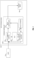
- Data storage device 100 may be a magnetic memory storage device, a FLASH memory storage device (including a NAND or NOR storage device), or some combination.
- Data storage device 100 may comprise a storage controller 102 and storage media 104.
- Storage controller 102 may perform one or more management actions to manage the storage media 104. For example, address translation that translates an address (e.g., a logical address) given in a read or write command from a host 116 to a physical address on the storage media 104.
- the storage controller 102 may include a flash translation layer that maps logical addresses to physical cells on the storage media 104.
- Storage controller 102 may also handle tasks such as garbage collection, wear levelling, encryption, defragmentation, and other tasks.
- Storage media 104 may include the physical storage media, such as NAND cells, NOR cells, magnetic media, and the like.
- storage controller 102 may perform one or more additional operations, including changing a value to be written to the storage media 104 if storage of the proposed value at the proposed location has a probability greater than a threshold of damaging other data on the storage media.
- proposed value and proposed location is the value and location specified by the host (e.g., the operating system or other application) in a write request issued to the data storage device 100.
- the storage controller 102 may include a host command control 106 which may receive commands from a host 116 - e.g., across a host interface (e.g., a Peripheral Component Interconnect Express - PCIE).
- Host 116 may send commands such as read, write, erase, and other commands to the storage controller 102 to perform operations on storage media 104.
- Host command control 106 may perform those commands and return a result to the host 116.
- host 116 may send a write command with a proposed data value and a proposed address.
- host command control 106 may translate the proposed address to a physical address on the storage media 104.
- the host command control 106 may apply an ECC operation to the proposed data value by sending the data to ECC component 108. While FIG. 1 shows ECC component 108 as part of the storage controller 102, in other examples, ECC component 108 may be a separate processor. ECC component 108 may return the data to the host command control 106 along with any ECC information needed.
- the host command control 106 may pass the returned ECC encoded proposed data value along with the physical address of the proposed location to a disturbance checker component 110.
- Disturbance checker component 110 may check to determine whether storage of the ECC encoded proposed value at the proposed location will cause interference to any non-targeted data storage units.
- the disturbance checker component 110 may track the number of read disturbs and/or program disturbs that have been experienced by each cell in the storage media 104. In some examples, this may be inefficient and so the disturbance checker component 110 may track these metrics on a higher level - such as at a data storage unit level, such as a page, sub-block, block, superblock, or other organizational level.
- the disturbance checker component 110 may determine the data storage units that are to be programmed (target data units) and determine a set of one or more other non-target data storage units that are likely to experience read and/or write disturb effects when a particular data storage unit is programmed.
- the disturbance checker component 110 may determine whether incrementing the read and/or program disturb counter for each particular non-target data storage unit puts any of the non-target data storage unit at risk by comparing the counter to one or more thresholds. For example, a first threshold may correspond to a first probability, a second threshold may correspond to a second probability, and so on. In other examples, the counters may be input to a formula that determines a probability that a non-target data storage unit would be impacted by writing the requested data
- the disturbance checker may compare the proposed data to be stored and the non-target data storage units to a pattern. For example, certain patterns may tend to produce higher probabilities of interference, for example, by creating large magnetic fields. These patterns may be stored in a working memory of the memory device or on the storage media 104 itself.
- certain repeated sequences of data may cause interference.
- the proposed value and the values stored in non-target data storage units may be examined to determine whether a density of a particular value is over a threshold, or whether a pattern of data matches stored patterns of data that have historically caused problems.
- a machine learning model may be utilized that predicts a probability of interference based upon the value to be stored and information about the non-target data storage units (e.g., neighboring memory pages, sectors, etc).
- the information about the non-target data storage units may include the value stored in the storage unit, the location of the non-target storage unit in relation to the location of the programmed storage unit and the value to be stored, and metadata about the non-target storage unit (e.g., read disturb and/or write disturb count, number of erasures, etc%) and information about the programmed storage unit. More information on the machine learning model is discussed in relation to FIG. 4 .
- Non-target data units are data units that are not being programmed or written by the requested write command.
- Target data units are data units that are being programmed or written by the requested write command.
- the system may analyze all non-target data units for interference potential, or only a subset of non-target data units that are neighboring data units.
- Neighboring data units may be determined by the structure of the storage media 104.
- neighboring data units may be non-target data units that are electrically or magnetically proximate to the target data units such that application of a charge or a current to, or storage of a value in, the target data unit may cause interference to the non-target data units.
- the disturbance checker component 110 may determine a new value to store.
- the probability may be a probability of affecting a single non-target data unit that is over a specified threshold. In these examples, it may not be valuable to introduce an error to prevent only one non-target error. In some examples, the probability may be a probability of affecting two or more non-target values. In these examples, introducing a correctable error to prevent multiple errors may be valuable. In still other examples, the system may distinguish between correctable errors that are introduced by writing the data and uncorrectable errors.
- the system may utilize one or more rules (e.g., if-then statements) to determine when to modify the data value before writing.
- the probability of a non-target data unit experiencing an uncorrectable error is greater than a first threshold AND the probability of the non-target data unit experiencing an uncorrectable error is reduced below a second threshold by introducing a correctable error on the data-to-be-written THEN introduce the correctable error on the data-to-be-written ELSE
- the probability of multiple non-target data units experiencing a correctable error is greater than a fourth threshold AND by introducing a correctable error on the data-to-be-written reduces the probability of multiple non-target data units experiencing a correctable error below a fifth threshold THEN introduce the correctable error on the data-to-be written.
- the value to change the data to may be determined through communication with the value changer 114.
- value changer 114 may have a table that maps data values to one or more changed data values. The table may be based upon experience that changing a first value to a second value may reduce the probability of interference to data values stored in non-target data units.
- the value changer 114 may provide one or more hypothesis for new values. These new values may be run through the disturbance checker component 110 to determine if the probability for interference is greater or lower than the original value. Probabilities for a series of these values may be calculated and the value that produces the lowest probability for interference may be selected.
- the ECC applied to the data allows for a set number of bit error corrections per specified unit of data written.
- the values produced by the value changer 114 may only change that many bits to ensure that the ECC error is correctable.
- the number of bit error corrections per specified unit may be lowered from the maximum for the given ECC based upon the condition of the media at the address the data will be written at For example, if that media location is wearing, has produced ECC errors in the past, or the like, the system may not use the full amount of bit errors that may be corrected in the anticipation that the media may add one or more unintentional errors
- the disturbance checker component 110 may provide the results to host command control 106, which may instruct the media controller 112 to write the new value to the storage media 104 at the proposed address.
- host command control 106 may instruct the media controller 112 to write the new value to the storage media 104 at the proposed address.
- the host 116 will issue a read command to the storage controller 102.
- the host command control 106 may command the media controller 112 to read the value at the given address from the storage media 104.
- the value will then fail the ECC check and may be corrected by the ECC component 108.
- the corrected value may then be provided to the host 116. If the ECC component 108 cannot correct the error, the host 116 is notified.
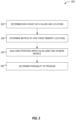
- FIG. 2 illustrates a flowchart of a method 200 of storing data in a data storage device according to some examples of the present disclosure.
- the memory device may receive a first data value for storage.
- the data value may be the proposed data value.
- the memory device may receive the first data value from a host device over a host interface.
- PCI-E Peripheral Component Interconnect Express
- SCSI Small Computer System Interface
- UFS Universal Flash Storage
- the host device may be a controller on the processor of a computing device of which the memory device is a part of.
- a processor a platform controller hub (PCH), a device driver, or the like.
- PCH platform controller hub
- the first data value may be received in a write request that requests the memory device write the first data value (the proposed data value) at a proposed memory address.
- the memory address given by the host may be translated into a physical memory address on the storage medium.
- a flash translation layer may translate the logical address provided by the host to one or more physical memory addresses. In some examples, this may include determining multiple addresses. For example, a byte of data may map to multiple memory cells or magnetic charges on the disk.
- the memory device may determine that placement of the first data value at the proposed location has a probability of causing interference with other non-target data units that is greater than a threshold probability.
- all non-target data units are analyzed, but in other examples, only neighboring data units may be analyzed.
- the physical memory addresses may have values stored in non-target (e.g., neighboring) data units that have a high read and/or write disturb count and writing the proposed data value may cause one or more of these non-target data units to increase in charge such that it reads a wrong value.
- placing the data at the proposed location may create one or more patterns that causes electrical or magnetic interference to other data.
- the patterns may be determined using one or more if-then rules that may consider the non-target data units, media state of the non-target data units, the location of the non-target data units relative to the written data, and the like.
- the patterns may be described by one or more data structures and the pattern that would result from writing the proposed data value at the physical address may be compared to a plurality of undesirable patterns.
- the undesirable patterns may be stored in the memory device. For example, if the request at operation 210 would cause a long run of same-valued data to be stored on a magnetic disk in a small area (i.e. a high density of a same value or a long run of a same data value), it may increase the probability of creating a self-demagnetization field and thus the probability at operation 220 may be above a threshold.
- the threshold probability at operation 220 may be a numerical threshold that may be specified by a designer of the memory device. In other examples, the probability at operation 220 may be a yes or no probability - e.g., if the proposed data value being written at the proposed address matches one of the undesirable patterns, the result of operation 220 may be a "yes.”
- the system may change the first data value to a second data value that reduces the probability of causing interference to one or more data values in non-target data units. For example, the system may change one or more bits of the data value and re-evaluate the changed data value using the methods disclosed for operation 220. The new data value with the lowest probability of causing interference to one or more non-targeted data values may be selected.
- the memory device may only change a number of bits that are correctable using the ECC applied to the first data values prior to changing it to the second data value. In some examples, the memory device may change fewer bits than are correctable using an ECC to ensure that minor disturbances on the media do not cause uncorrectable ECC errors.
- the memory device may write the second value to the media of the data storage device at the proposed location.
- the ECC information e.g., a parity check value, or the like
- the controller may spin the magnetic disks to the proper track and sector and cause application of a magnetic field to write the second value.
- a program voltage is applied to one or more memory cells of flash memory (e.g., NAND or NOR).
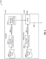
- FIG. 3 illustrates a flowchart of a method 300 of determining a probability that the placement of the first data value at a proposed location has a probability of causing interference with other data that is greater than a threshold probability according to some examples of the present disclosure.
- the method 300 may be one example of operation 220 of FIG. 2 .
- the memory device may determine non-target data storage units to the proposed address. In some examples, this may be neighboring data units as defined above. In some examples, this may include non-target data values within a threshold distance on the physical media from the one or more storage units used to store the data value at the requested storage location. For example, data that is physically stored on the media in a location that is adjacent to the requested storage location. For example, a same sector on adjacent tracks, a same track on adjacent sectors, or the like. In examples in which the memory device is a NAND memory device, memory cells that are on adjacent word lines, adjacent page lines, and the like.
- the memory device may analyze the proposed value using one or more models.
- the models may be if-then-else rules.
- the models may be one or more nested sets of ifthen-else rules such as a decision tree.
- the rules may model placements of data, such as rules specifying a maximum run-length of a particular value, a maximum density of a particular value in a particular area (e.g., within a radius of x data units, there can only be a maximum of y same bit values).
- rules may specify a maximum threshold of reads, writes, or other values for non-target data units before a probability of an error in a non-targeted data unit exceeds a threshold.
- machine-learned models may be utilized that may take as input the proposed value and the proposed location and information on values in non-target data units and their locations respective to the proposed location. Additionally, the machine-learned models may also use information on the status of the media for the data units making up the proposed location and the non-target data units. For example, a read-disturb counter, write-disturb counter, a number of reads, a number of writes, and the like. The machine-learned model may be trained on a large corpus of historical data writes and may be labelled on whether a subsequent read of non-target data units resulted in an ECC error. The machine-learned model may thus be trained to predict the likelihood of an ECC error. More information on machine-learned models is shown in FIG. 4 .
- the results of the models may be used to determine whether a probability of a non-target data unit being interfered with by writing the requested value at the requested location is above a threshold.
- a single rule may be evaluated, and the result of the evaluation may be used to determine the probability. For example, a comparison may yield a match between the proposed value at the proposed location, non-target values, and one or more undesirable data patterns. In these examples, finding a match with an undesirable data pattern may cause the result of operation 340 to return true - that the probability is above a threshold.
- multiple rules may be evaluated.
- the system may return that the probability is above a threshold that a non-target data unit may be interfered with by the placement of the requested value at the proposed location if one or more rules return true, or if a combination of rules returns true as specified by one or more Boolean logical connectors between rules (e.g., AND, OR, NOR, XOR).
- each of multiple rules may produce a sub score that may be weighted and combined to produce a value, which, if the value exceeds a threshold, the system indicates that the placement of the proposed value in the proposed location may cause interference to data in non-targeted data units.
- operation 340 utilizes the results of the machine-learned model.
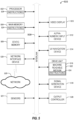
- FIG. 4 illustrates an example machine learning module 400 according to some examples of the present disclosure.
- the machine learning module 400 may be implemented in whole or in part by the storage controller 102.
- the training module 410 may be implemented by a different device than the prediction module 420.
- the model 480 may be created on a first machine and then sent to a second machine.
- Machine learning module 400 utilizes a training module 410 and a prediction module 420.
- Training module 410 inputs feature data 430 into feature determination module 450.
- Feature determination module 450 determines one or more features for feature vector 460 from the feature data 430.
- Features chosen for inclusion in the feature vector 460 may be all the feature data 430 or in some examples, may be a subset of all the feature data 430. In examples in which the features chosen for the feature vector 460 are a subset of the feature data 430, a predetermined list of which feature data 430 is included in the feature vector may be utilized.
- the feature vector 460 may be utilized (along with any applicable labels) by the machine learning algorithm 470 to produce a model 480.
- the current feature data 490 of the user may be input to the feature determination module 495.
- Feature determination module 495 may determine the same set of features or a different set of features as feature determination module 450. In some examples, feature determination module 450 and 495 are the same modules or different instances of the same module. Feature determination module 495 produces feature vector 497, which are input into the model 480 to produce results 499.
- the training module 410 may operate in an offline manner to train the model 480.
- the prediction module 420 may be designed to operate in an online manner. It should be noted that the model 480 may be periodically updated via additional training and/or user feedback.
- the machine learning algorithm 470 may be selected from among many different potential supervised or unsupervised machine learning algorithms.
- Examples of supervised learning algorithms include artificial neural networks, convolutional neural networks, Bayesian networks, instance-based learning, support vector machines, decision trees (e.g., Iterative Dichotomiser 3, C4.5, Classification and Regression Tree (CART), Chi-squared Automatic Interaction Detector (CHAID), and the like),random forests, linear classifiers, quadratic classifiers, k-nearest neighbor, linear regression, logistic regression, and hidden Markov models.
- Examples of unsupervised learning algorithms include expectation-maximization algorithms, vector quantization, and information bottleneck method. Unsupervised models may not have a training module 410 or may not utilize labels on feature data 430.
- the model 480 may be utilized in some examples to determine whether placement of the proposed value at the proposed location is likely to cause errors to values in non-target data units.
- the feature data 430 may include historical data storage requests including the proposed value and location as well as one or more of: the non-target data units locations relative to the value and location, information about the data units making up the proposed location and non-target data units (e.g., such as the number of previous writes, erases, reads, read-disturb counters, write-disturb counters, and the like), or the like.
- the feature data 430 may be labeled with an indication of whether and which non-target data units experienced an ECC error that corresponds to the proposed write.
- Feature data 490 includes the current proposed value and location as well as one or more of: the non-target data units locations relative to the value and location, information about the data units making up the proposed location and non-target data units (e.g., such as the number of previous writes, erases, reads, read-disturb counters, write-disturb counters, and the like), or the like.
- the model 480 may provide a probability that the proposed write may introduce one or more errors into the data or may be an indication of whether one or more errors are likely to be introduced.
- the system modifies the proposed value if the probability of a single error being introduced in a single non-target data unit exceeds a threshold. In other examples, the system may modify the proposed value only if the probability of multiple errors being introduced in multiple non-target data units exceeds a threshold or if the single error in the single non-target data unit would be an uncorrectable ECC error.
- FIG. 5 illustrates a block diagram of an example machine 500 that may implement any one or more of the techniques (e.g., methodologies) discussed herein.
- the host device may include the machine 500 and the memory device may be the main memory 504, static memory 506, drive unit 516, or the like.
- the memory device may also include one or more of the components of FIG. 5 , such as processor 502, main memory 504 (including instructions 524), and the like.
- the machine 500 may operate as a standalone device or may be connected (e.g., networked) to other machines.
- Machine 500 may implement the data storage device 100, a device implementing host 116, and perform the methods of FIGs. 2 and 3 and implement one or more of the machine-learning modules of FIG. 4 .
- the machine 500 may operate in the capacity of a server machine, a client machine, or both in server-client network environments.
- the machine 500 may act as a peer machine in peer-to-peer (P2P) (or other distributed) network environment.
- the machine 500 may be a memory device, a personal computer (PC), a tablet PC, a set-top box (STB), a personal digital assistant (PDA), a mobile telephone, a smart phone, a web appliance, a network router, switch or bridge, or any machine capable of executing instructions (sequential or otherwise) that specify actions to be taken by that machine.
- machine shall also be taken to include any collection of machines that individually or jointly execute a set (or multiple sets) of instructions to perform any one or more of the methodologies discussed herein, such as cloud computing, software as a service (SaaS), other computer cluster configurations.
- cloud computing software as a service
- SaaS software as a service
- Examples, as described herein, may include, or may operate on, logic or a number of components, modules, or mechanisms.
- Modules are tangible entities (e.g., hardware) capable of performing specified operations and may be configured or arranged in a certain manner.
- circuits may be arranged (e.g., internally or with respect to external entities such as other circuits) in a specified manner as a module.
- the whole or part of one or more computer systems e.g., a standalone, client or server computer system
- one or more hardware processors may be configured by firmware or software (e.g., instructions, an application portion, or an application) as a module that operates to perform specified operations.
- the software may reside on a machine readable medium.
- the software when executed by the underlying hardware of the module, causes the hardware to perform the specified operations.
- module is understood to encompass a tangible entity, be that an entity that is physically constructed, specifically configured (e.g., hardwired), or temporarily (e.g., transitorily) configured (e.g., programmed) to operate in a specified manner or to perform part or all of any operation described herein.
- each of the modules need not be instantiated at any one moment in time.
- the modules comprise a general-purpose hardware processor configured using software
- the general-purpose hardware processor may be configured as respective different modules at different times.
- Software may accordingly configure a hardware processor, for example, to constitute a particular module at one instance of time and to constitute a different module at a different instance of time.
- Machine 500 may include a hardware processor 502 (e.g., a central processing unit (CPU), a graphics processing unit (GPU), a hardware processor core, or any combination thereof), a main memory 504 and a static memory 506, some or all of which may communicate with each other via an interlink (e.g., bus) 508.
- the machine 500 may further include a display unit 510, an alphanumeric input device 512 (e.g., a keyboard), and a user interface (UI) navigation device 514 (e.g., a mouse).
- the display unit 510, input device 512 and UI navigation device 514 may be a touch screen display.
- the machine 500 may additionally include a storage device (e.g., drive unit) 516, a signal generation device 518 (e.g., a speaker), a network interface device 520, and one or more sensors 521, such as a global positioning system (GPS) sensor, compass, accelerometer, or other sensor.
- the machine 500 may include an output controller 528, such as a serial (e.g., universal serial bus (USB), parallel, or other wired or wireless (e.g., infrared(IR), near field communication (NFC), etc.) connection to communicate or control one or more peripheral devices (e.g., a printer, card reader, etc.).
- a serial e.g., universal serial bus (USB), parallel, or other wired or wireless (e.g., infrared(IR), near field communication (NFC), etc.) connection to communicate or control one or more peripheral devices (e.g., a printer, card reader, etc.).
- USB universal serial bus
- NFC near field
- the storage device 516 may include a machine readable medium 522 on which is stored one or more sets of data structures or instructions 524 (e.g., software) embodying or utilized by any one or more of the techniques or functions described herein.
- the instructions 524 may also reside, completely or at least partially, within the main memory 504, within static memory 506, or within the hardware processor 502 during execution thereof by the machine 500.
- one or any combination of the hardware processor 502, the main memory 504, the static memory 506, or the storage device 516 may constitute machine readable media.
- machine readable medium 522 is illustrated as a single medium, the term “machine readable medium” may include a single medium or multiple media (e.g., a centralized or distributed database, and/or associated caches and servers) configured to store the one or more instructions 524.
- machine readable medium may include a single medium or multiple media (e.g., a centralized or distributed database, and/or associated caches and servers) configured to store the one or more instructions 524.
- machine readable medium may include any medium that is capable of storing, encoding, or carrying instructions for execution by the machine 500 and that cause the machine 500 to perform any one or more of the techniques of the present disclosure, or that is capable of storing, encoding or carrying data structures used by or associated with such instructions.
- Non-limiting machine readable medium examples may include solid-state memories, and optical and magnetic media.
- machine readable media may include: non-volatile memory, such as semiconductor memory devices (e.g., Electrically Programmable Read-Only Memory (EPROM), Electrically Erasable Programmable Read-Only Memory (EEPROM)) and flash memory devices; magnetic disks, such as internal hard disks and removable disks; magneto-optical disks; Random Access Memory (RAM); Solid State Drives (SSD); and CD-ROM and DVD-ROM disks.
- EPROM Electrically Programmable Read-Only Memory
- EEPROM Electrically Erasable Programmable Read-Only Memory
- flash memory devices e.g., Electrically Programmable Read-Only Memory (EPROM), Electrically Erasable Programmable Read-Only Memory (EEPROM)
- flash memory devices e.g., Electrically Programmable Read-Only Memory (EPROM), Electrically Erasable Programmable Read-Only Memory (EEPROM)
- flash memory devices e.g., Electrically Programmable Read-Only Memory (EPROM), Electrically Erasable Programmable
- the instructions 524 may further be transmitted or received over a communications network 526 using a transmission medium via the network interface device 520.
- the Machine 500 may communicate with one or more other machines utilizing any one of a number of transfer protocols (e.g., frame relay, internet protocol (IP), transmission control protocol (TCP), user datagram protocol (UDP), hypertext transfer protocol (HTTP), etc.).
- transfer protocols e.g., frame relay, internet protocol (IP), transmission control protocol (TCP), user datagram protocol (UDP), hypertext transfer protocol (HTTP), etc.
- Example communication networks may include a local area network (LAN), a wide area network (WAN), a packet data network (e.g., the Internet), mobile telephone networks (e.g., cellular networks), Plain Old Telephone (POTS) networks, and wireless data networks (e.g., Institute of Electrical and Electronics Engineers (IEEE) 802.11 family of standards known as Wi-Fi ® , IEEE 802.16 family of standards known as WiMax ® ), IEEE 802.15.4 family of standards, a Long Term Evolution (LTE) family of standards, a Universal Mobile Telecommunications System (UMTS) family of standards, peer-to-peer (P2P) networks, among others.
- LAN local area network
- WAN wide area network
- POTS Plain Old Telephone
- wireless data networks e.g., Institute of Electrical and Electronics Engineers (IEEE) 802.11 family of standards known as Wi-Fi ® , IEEE 802.16 family of standards known as WiMax ®
- IEEE 802.15.4 family of standards e.g., a Long
- the network interface device 520 may include one or more physical jacks (e.g., Ethernet, coaxial, or phone jacks) or one or more antennas to connect to the communications network 526.
- the network interface device 520 may include a plurality of antennas to wirelessly communicate using at least one of single-input multiple-output (SIMO), multiple-input multiple-output (MIMO), or multiple-input single-output (MISO) techniques.
- SIMO single-input multiple-output
- MIMO multiple-input multiple-output
- MISO multiple-input single-output
- the network interface device 520 may wirelessly communicate using Multiple User MIMO techniques.
Landscapes
- Engineering & Computer Science (AREA)
- Theoretical Computer Science (AREA)
- Physics & Mathematics (AREA)
- General Engineering & Computer Science (AREA)
- General Physics & Mathematics (AREA)
- Microelectronics & Electronic Packaging (AREA)
- Human Computer Interaction (AREA)
- Quality & Reliability (AREA)
- Computer Hardware Design (AREA)
- Techniques For Improving Reliability Of Storages (AREA)
Description
- Magnetic storage devices encode bits as a directional alignment of magnetic charges on a magnetic media. For example, a hard disk utilizes one or more spinning platters of metal with magnetic particles affixed to them. To write data, a write head moves to a specific location of one of the spinning platters and electrical current is applied to an electromagnet of the write head which generates a magnetic field which aligns the magnetic charges of the magnetic particles in that location along a certain direction. A first alignment direction may encode a '1' and a second alignment direction may encode a '0'. Later, to read the data, a read head reads the alignment direction of the magnetic charges to determine the stored bit. Magnetic storage devices typically store data in concentric rings called tracks. Portions of tracks are called sectors. Depending on the data storage device, sectors may store 512 bytes, 2048 bytes, 4096 bytes, and the like.
- Solid state flash memory devices, such as NAND memory devices, store data as charges in semiconductor floating gate transistors. Charges are stored on individual semiconductor cells by applying a programming voltage to these cells. Different charge levels are assigned to different bit values or bit value combinations. In a Single Level Cell (SLC) - which stores only one bit per cell - a first charge level represents a '1' and a second charge level may represent a '0'. In a multi-level cell (MLC), two bits may be stored by use of four different charge levels. In a triple level cell (TLC), three bits may be stored by using eight charge levels, and so on.
-
US2011066902A1 discloses reading data using a reliability measure in which a reliability measure is computed for at least one bit stored in the target memory cell of a memory array based on a voltage value associated with the target memory cell and based on one or more corresponding voltage values associated with each of the one or more other memory cells of the memory array. -
US2010223530A1 discloses a semiconductor memory device in which data is rearranged by various operations such as a modulation code operation and the data is processed according to an ECC operation to reduce the interference between memory cells. - The invention is defined by the appended independent claims.
- In the drawings, which are not necessarily drawn to scale, like numerals may describe similar components in different views. Like numerals having different letter suffixes may represent different instances of similar components. The drawings illustrate generally, by way of example, but not by way of limitation, various embodiments discussed in the present document.
-
FIG. 1 illustrates a data storage device according to some examples of the present disclosure. -
FIG. 2 illustrates a flowchart of a method of storing data in a data storage device according to some examples of the present disclosure. -
FIG. 3 illustrates a flowchart of a method of determining a probability that the placement of the first data value at an indicated location has a probability of causing interference with other data that is greater than a threshold probability according to some examples of the present disclosure. -
FIG. 4 illustrates an example machine learning module according to some examples of the present disclosure. -
FIG. 5 is a block diagram illustrating an example of a machine upon which one or more embodiments may be implemented. - While magnetic and solid-state storage technologies have much different structures and methods of operation, they both rely upon the encoding of data as electrons or magnetic charge to represent the 1's and 0's of data. Both electrons stored in a semiconductor and magnetic charge stored on a magnetic medium are subject to interference. For example, a magnetic hard drive has a plurality of circular tracks that each have a plurality of sectors. To meet the demand for increased storage, hard drives have increased the density of the tracks, sectors, and the like. By reducing the size of the magnetic grains that store the magnetic charge the hard drive can store more data. As the charges becomes closer and closer together, the magnetic charge becomes more susceptible to spontaneous switching of its state of magnetization. This susceptibility increases with increases in temperature. In some examples, to solve this problem, some hard drives store their charge perpendicularly - that is, the magnetic grains are perpendicularly oriented to the plane of the media. In these devices, problems still exist where a long run length of a same value can cause a demagnetization field that causes a self-demagnetization force that tries to switch back a magnetization state of the grains within the region. These problems may affect multiple neighboring sectors.
- Similarly, for solid state devices, the structure of NAND devices into word lines, pages, and blocks creates certain challenges. In NAND flash, memory cells are organized into two dimensional arrays called blocks. In each block, cells in a same row share a wordline and cells in a same column share a bitline. A page is the smallest data unit that may be programmed and read and is made up of cells connected on a same wordline. To write data to a NAND cell, a programming voltage is applied to the cell and this voltage increases the charge level to the desired range that represents the value being stored. This programming voltage may cause cell-to-cell program interference to adjacent memory cells that are not being programmed because charge from this programming voltage increases the charge level in those neighboring cells due to the interconnections of the cells. This effect is called program-disturb. If the cumulative effect of many programming voltages being applied to neighboring cells increases the charge level enough, it may change the value stored in the cell. For MLC, TLC and other cells, each cell is programmed using multiple steps to reduce the impact of this interference. Despite the use of multiple steps, programming interference is still an issue in modern NAND devices.
- To read a page of NAND flash, a read voltage is applied to the wordline that contains the data to be read and sense amplifiers connected to the bitlines determine the value in the cell. To read MLC and TLC cells, multiple read voltages of different threshold voltage levels may be applied. A passthrough voltage is applied to cells of other wordlines connected to the same bitlines that are being read. The passthrough voltage is not as high as the programming voltage, but still induces a weak programming effect on those cells. This is called read-disturb. As with the program disturb, enough cumulative read-disturb incidents may cause a change in the value of a cell.
- Both storage device types rely upon a number of mechanisms to deal with the errors mentioned above. For example, some NAND devices track the number of reads and writes that impact a cell as a read-disturb counter and a program-disturb counter. Each time a neighboring cell is read, the read-disturb counter for that cell is incremented. Similarly, each time a neighboring cell is programmed, the program-disturb counter may be incremented. Various actions may be taken when the read and/or program-disturb counter exceeds a threshold to ensure that the data is not compromised. For example, the data may be read and rewritten in a different cell.
- Both flash memory and magnetic storage typically also use error correction codes (ECC) to detect, and correct errors caused by the mechanisms described above and other errors. Error correction codes may detect and correct a defined number of errors for a particular number of bits stored in the memory devices. The ECC is applied to the data prior to it being written to the storage medium and one or more ECC values may also be stored on the storage medium. If the errors caused by the mechanisms noted above are too numerous, they may exceed the ability of the ECC to correct the errors and the data may be irretrievably lost. For example, if the read-disturb errors change too many bits, the ECC may not be able to detect and/or correct the errors. Example ECC algorithms include block codes (e.g., Hamming codes), cyclic codes, BCH (Bose-Chaudhri-Hocquenghem) codes, Reed-Solomon codes, Convolutional codes (including Viterbi codes), and the like. ECC algorithms may include Forward Error Correction (FEC). While ECC algorithms are traditionally used to correct errors after they occur, they have not been used to actively prevent errors.
- Disclosed in some examples are methods, systems, storage devices, and machine readable mediums that utilize the ability of ECC to correct errors to actively prevent errors. The memory device determines whether a request to place data of a requested value at a requested location in the storage media is likely to interfere with other data stored at other locations on the storage media, and if so, changes the requested value to a second value that will not interfere (or has a lower probability of interfering) with neighboring data. The second value may be corrected to the requested value when a read request is made for that data using ECC. That is, the ECC information may be generated on the requested value and the second value (which is actually stored) may be later corrected to the requested value using the ECC information. The second value may be chosen to be less destructive and/or interfering to neighboring data while at the same time, being close enough to the requested value to be correctable by the ECC. While intentionally introducing an error to reduce errors may seem counterintuitive, introducing a single correctable error to reduce the probability of multiple errors or one or more uncorrectable errors may reduce an overall error rate. As used herein, a data storage unit is a storage location on a physical media for a single unit of data. For example, a sector on a magnetic media, or a page on flash memory, or the like. While the techniques described herein are described as applying to a unit of data, it will be appreciated by one of ordinary skill that the techniques may be applied to smaller units of storage, such as a single NAND cell, or a location where a single bit is stored on magnetic media.
- Turning now to
FIG. 1 adata storage device 100 is shown according to some examples of the present disclosure.Data storage device 100 may be a magnetic memory storage device, a FLASH memory storage device (including a NAND or NOR storage device), or some combination.Data storage device 100 may comprise astorage controller 102 andstorage media 104.Storage controller 102 may perform one or more management actions to manage thestorage media 104. For example, address translation that translates an address (e.g., a logical address) given in a read or write command from ahost 116 to a physical address on thestorage media 104. For example, thestorage controller 102 may include a flash translation layer that maps logical addresses to physical cells on thestorage media 104.Storage controller 102 may also handle tasks such as garbage collection, wear levelling, encryption, defragmentation, and other tasks.Storage media 104 may include the physical storage media, such as NAND cells, NOR cells, magnetic media, and the like. - In addition to the functions described above,
storage controller 102 may perform one or more additional operations, including changing a value to be written to thestorage media 104 if storage of the proposed value at the proposed location has a probability greater than a threshold of damaging other data on the storage media. As used herein, proposed value and proposed location is the value and location specified by the host (e.g., the operating system or other application) in a write request issued to thedata storage device 100. For example, thestorage controller 102 may include ahost command control 106 which may receive commands from a host 116 - e.g., across a host interface (e.g., a Peripheral Component Interconnect Express - PCIE). Host 116 may send commands such as read, write, erase, and other commands to thestorage controller 102 to perform operations onstorage media 104.Host command control 106 may perform those commands and return a result to thehost 116. For example, host 116 may send a write command with a proposed data value and a proposed address. Upon receiving the write command,host command control 106 may translate the proposed address to a physical address on thestorage media 104. Thehost command control 106 may apply an ECC operation to the proposed data value by sending the data toECC component 108. WhileFIG. 1 showsECC component 108 as part of thestorage controller 102, in other examples,ECC component 108 may be a separate processor.ECC component 108 may return the data to thehost command control 106 along with any ECC information needed. - The
host command control 106 may pass the returned ECC encoded proposed data value along with the physical address of the proposed location to adisturbance checker component 110.Disturbance checker component 110 may check to determine whether storage of the ECC encoded proposed value at the proposed location will cause interference to any non-targeted data storage units. - For solid state devices, in some examples, the
disturbance checker component 110 may track the number of read disturbs and/or program disturbs that have been experienced by each cell in thestorage media 104. In some examples, this may be inefficient and so thedisturbance checker component 110 may track these metrics on a higher level - such as at a data storage unit level, such as a page, sub-block, block, superblock, or other organizational level. Thedisturbance checker component 110 may determine the data storage units that are to be programmed (target data units) and determine a set of one or more other non-target data storage units that are likely to experience read and/or write disturb effects when a particular data storage unit is programmed. Thedisturbance checker component 110 may determine whether incrementing the read and/or program disturb counter for each particular non-target data storage unit puts any of the non-target data storage unit at risk by comparing the counter to one or more thresholds. For example, a first threshold may correspond to a first probability, a second threshold may correspond to a second probability, and so on. In other examples, the counters may be input to a formula that determines a probability that a non-target data storage unit would be impacted by writing the requested data - For magnetic devices such as hard disk drives, the disturbance checker may compare the proposed data to be stored and the non-target data storage units to a pattern. For example, certain patterns may tend to produce higher probabilities of interference, for example, by creating large magnetic fields. These patterns may be stored in a working memory of the memory device or on the
storage media 104 itself. - For either magnetic storage devices or flash devices, certain repeated sequences of data (e.g., runs of '0's or '1's) may cause interference. In these examples, the proposed value and the values stored in non-target data storage units may be examined to determine whether a density of a particular value is over a threshold, or whether a pattern of data matches stored patterns of data that have historically caused problems.
- In still other examples, a machine learning model may be utilized that predicts a probability of interference based upon the value to be stored and information about the non-target data storage units (e.g., neighboring memory pages, sectors, etc...). The information about the non-target data storage units may include the value stored in the storage unit, the location of the non-target storage unit in relation to the location of the programmed storage unit and the value to be stored, and metadata about the non-target storage unit (e.g., read disturb and/or write disturb count, number of erasures, etc...) and information about the programmed storage unit. More information on the machine learning model is discussed in relation to
FIG. 4 . - Non-target data units are data units that are not being programmed or written by the requested write command. Target data units are data units that are being programmed or written by the requested write command. The system may analyze all non-target data units for interference potential, or only a subset of non-target data units that are neighboring data units. Neighboring data units may be determined by the structure of the
storage media 104. For example, neighboring data units may be non-target data units that are electrically or magnetically proximate to the target data units such that application of a charge or a current to, or storage of a value in, the target data unit may cause interference to the non-target data units. - If the
disturbance checker component 110 determines that there exists a probability that writing this value to the selected location may cause other data storage units to be interfered with, thedisturbance checker component 110 may determine a new value to store. In some examples, the probability may be a probability of affecting a single non-target data unit that is over a specified threshold. In these examples, it may not be valuable to introduce an error to prevent only one non-target error. In some examples, the probability may be a probability of affecting two or more non-target values. In these examples, introducing a correctable error to prevent multiple errors may be valuable. In still other examples, the system may distinguish between correctable errors that are introduced by writing the data and uncorrectable errors. That is, if a non-target data unit were to experience an uncorrectable ECC error because of the data write, then it would be valuable to introduce a correctable ECC error in the data to be written to prevent the uncorrectable ECC of a non-target data value. Thus, the system may utilize one or more rules (e.g., if-then statements) to determine when to modify the data value before writing. For example:
IF the probability of a non-target data unit experiencing an uncorrectable error is greater than a first threshold AND the probability of the non-target data unit experiencing an uncorrectable error is reduced below a second threshold by introducing a correctable error on the data-to-be-written THEN introduce the correctable error on the data-to-be-written ELSE IF the probability of multiple non-target data units experiencing a correctable error is greater than a fourth threshold AND by introducing a correctable error on the data-to-be-written reduces the probability of multiple non-target data units experiencing a correctable error below a fifth threshold THEN introduce the correctable error on the data-to-be written. - In some examples, the value to change the data to may be determined through communication with the
value changer 114. For example,value changer 114 may have a table that maps data values to one or more changed data values. The table may be based upon experience that changing a first value to a second value may reduce the probability of interference to data values stored in non-target data units. In some examples, thevalue changer 114 may provide one or more hypothesis for new values. These new values may be run through thedisturbance checker component 110 to determine if the probability for interference is greater or lower than the original value. Probabilities for a series of these values may be calculated and the value that produces the lowest probability for interference may be selected. - In some examples, the ECC applied to the data allows for a set number of bit error corrections per specified unit of data written. In these examples, the values produced by the
value changer 114 may only change that many bits to ensure that the ECC error is correctable. In other examples, the number of bit error corrections per specified unit may be lowered from the maximum for the given ECC based upon the condition of the media at the address the data will be written at For example, if that media location is wearing, has produced ECC errors in the past, or the like, the system may not use the full amount of bit errors that may be corrected in the anticipation that the media may add one or more unintentional errors - Once the new value is calculated, the
disturbance checker component 110 may provide the results to hostcommand control 106, which may instruct themedia controller 112 to write the new value to thestorage media 104 at the proposed address. When thehost 116 wishes to read this value from the address, thehost 116 will issue a read command to thestorage controller 102. Thehost command control 106 may command themedia controller 112 to read the value at the given address from thestorage media 104. The value will then fail the ECC check and may be corrected by theECC component 108. The corrected value may then be provided to thehost 116. If theECC component 108 cannot correct the error, thehost 116 is notified. -
FIG. 2 illustrates a flowchart of amethod 200 of storing data in a data storage device according to some examples of the present disclosure. Atoperation 210 the memory device may receive a first data value for storage. The data value may be the proposed data value. The memory device may receive the first data value from a host device over a host interface. For example, from a host device over a Peripheral Component Interconnect Express (PCI-E) interface, a Small Computer System Interface (SCSI), a Universal Flash Storage (UFS) interface, and the like. The host device may be a controller on the processor of a computing device of which the memory device is a part of. For example, a processor, a platform controller hub (PCH), a device driver, or the like. The first data value may be received in a write request that requests the memory device write the first data value (the proposed data value) at a proposed memory address. The memory address given by the host may be translated into a physical memory address on the storage medium. For example, a flash translation layer may translate the logical address provided by the host to one or more physical memory addresses. In some examples, this may include determining multiple addresses. For example, a byte of data may map to multiple memory cells or magnetic charges on the disk. - At operation 220, the memory device may determine that placement of the first data value at the proposed location has a probability of causing interference with other non-target data units that is greater than a threshold probability. In some examples, all non-target data units are analyzed, but in other examples, only neighboring data units may be analyzed. For example, the physical memory addresses may have values stored in non-target (e.g., neighboring) data units that have a high read and/or write disturb count and writing the proposed data value may cause one or more of these non-target data units to increase in charge such that it reads a wrong value. In other examples, placing the data at the proposed location may create one or more patterns that causes electrical or magnetic interference to other data. The patterns may be determined using one or more if-then rules that may consider the non-target data units, media state of the non-target data units, the location of the non-target data units relative to the written data, and the like. In other examples, the patterns may be described by one or more data structures and the pattern that would result from writing the proposed data value at the physical address may be compared to a plurality of undesirable patterns. The undesirable patterns may be stored in the memory device. For example, if the request at
operation 210 would cause a long run of same-valued data to be stored on a magnetic disk in a small area (i.e. a high density of a same value or a long run of a same data value), it may increase the probability of creating a self-demagnetization field and thus the probability at operation 220 may be above a threshold. - The threshold probability at operation 220 may be a numerical threshold that may be specified by a designer of the memory device. In other examples, the probability at operation 220 may be a yes or no probability - e.g., if the proposed data value being written at the proposed address matches one of the undesirable patterns, the result of operation 220 may be a "yes."
- At
operation 230, the system may change the first data value to a second data value that reduces the probability of causing interference to one or more data values in non-target data units. For example, the system may change one or more bits of the data value and re-evaluate the changed data value using the methods disclosed for operation 220. The new data value with the lowest probability of causing interference to one or more non-targeted data values may be selected. In some examples, the memory device may only change a number of bits that are correctable using the ECC applied to the first data values prior to changing it to the second data value. In some examples, the memory device may change fewer bits than are correctable using an ECC to ensure that minor disturbances on the media do not cause uncorrectable ECC errors. - At
operation 240, the memory device may write the second value to the media of the data storage device at the proposed location. In some examples, the ECC information (e.g., a parity check value, or the like) from the originally proposed value may also be written. For example, the controller may spin the magnetic disks to the proper track and sector and cause application of a magnetic field to write the second value. In other examples, a program voltage is applied to one or more memory cells of flash memory (e.g., NAND or NOR). -
FIG. 3 illustrates a flowchart of amethod 300 of determining a probability that the placement of the first data value at a proposed location has a probability of causing interference with other data that is greater than a threshold probability according to some examples of the present disclosure. Themethod 300 may be one example of operation 220 ofFIG. 2 . Atoperation 320, the memory device may determine non-target data storage units to the proposed address. In some examples, this may be neighboring data units as defined above. In some examples, this may include non-target data values within a threshold distance on the physical media from the one or more storage units used to store the data value at the requested storage location. For example, data that is physically stored on the media in a location that is adjacent to the requested storage location. For example, a same sector on adjacent tracks, a same track on adjacent sectors, or the like. In examples in which the memory device is a NAND memory device, memory cells that are on adjacent word lines, adjacent page lines, and the like. - At
operation 325, in some examples, the memory device may determine metrics of one or more of the non-target data storage units determined inoperation 320. For example, one or more of a read-disturb count, a write-disturb count, a number of uncorrectable ECC errors associated with those locations, a write count, a read count, and the like. In some examples, the metrics may be individualized to each data storage unit (e.g., each memory cell, or each bit storage unit on a hard drive), but in other examples, the metrics may be generalized to one or more groups of data storage units. For example, a page of NAND cells, a sector of a magnetic hard disk, or the like. - At
operation 330, the memory device may analyze the proposed value using one or more models. In some examples, the models may be if-then-else rules. In some examples, the models may be one or more nested sets of ifthen-else rules such as a decision tree. For example, the rules may model placements of data, such as rules specifying a maximum run-length of a particular value, a maximum density of a particular value in a particular area (e.g., within a radius of x data units, there can only be a maximum of y same bit values). In some examples, rules may specify a maximum threshold of reads, writes, or other values for non-target data units before a probability of an error in a non-targeted data unit exceeds a threshold. - In other examples, machine-learned models may be utilized that may take as input the proposed value and the proposed location and information on values in non-target data units and their locations respective to the proposed location. Additionally, the machine-learned models may also use information on the status of the media for the data units making up the proposed location and the non-target data units. For example, a read-disturb counter, write-disturb counter, a number of reads, a number of writes, and the like. The machine-learned model may be trained on a large corpus of historical data writes and may be labelled on whether a subsequent read of non-target data units resulted in an ECC error. The machine-learned model may thus be trained to predict the likelihood of an ECC error. More information on machine-learned models is shown in
FIG. 4 . - At
operation 340, the results of the models may be used to determine whether a probability of a non-target data unit being interfered with by writing the requested value at the requested location is above a threshold. In some examples, at operation 330 a single rule may be evaluated, and the result of the evaluation may be used to determine the probability. For example, a comparison may yield a match between the proposed value at the proposed location, non-target values, and one or more undesirable data patterns. In these examples, finding a match with an undesirable data pattern may cause the result ofoperation 340 to return true - that the probability is above a threshold. In some examples, atoperation 330 multiple rules may be evaluated. For example, the system may return that the probability is above a threshold that a non-target data unit may be interfered with by the placement of the requested value at the proposed location if one or more rules return true, or if a combination of rules returns true as specified by one or more Boolean logical connectors between rules (e.g., AND, OR, NOR, XOR). In some examples, rather than use Boolean logical rules, each of multiple rules may produce a sub score that may be weighted and combined to produce a value, which, if the value exceeds a threshold, the system indicates that the placement of the proposed value in the proposed location may cause interference to data in non-targeted data units. In other examples, for machine-learned models,operation 340 utilizes the results of the machine-learned model. -
FIG. 4 illustrates an examplemachine learning module 400 according to some examples of the present disclosure. Themachine learning module 400 may be implemented in whole or in part by thestorage controller 102. In some examples, thetraining module 410 may be implemented by a different device than theprediction module 420. In these examples, themodel 480 may be created on a first machine and then sent to a second machine. -
Machine learning module 400 utilizes atraining module 410 and aprediction module 420.Training module 410 inputs featuredata 430 intofeature determination module 450.Feature determination module 450 determines one or more features forfeature vector 460 from thefeature data 430. Features chosen for inclusion in thefeature vector 460 may be all thefeature data 430 or in some examples, may be a subset of all thefeature data 430. In examples in which the features chosen for thefeature vector 460 are a subset of thefeature data 430, a predetermined list of which featuredata 430 is included in the feature vector may be utilized. Thefeature vector 460 may be utilized (along with any applicable labels) by themachine learning algorithm 470 to produce amodel 480. - In the
prediction module 420, thecurrent feature data 490 of the user may be input to thefeature determination module 495.Feature determination module 495 may determine the same set of features or a different set of features asfeature determination module 450. In some examples,feature determination module Feature determination module 495 producesfeature vector 497, which are input into themodel 480 to produceresults 499. - The
training module 410 may operate in an offline manner to train themodel 480. Theprediction module 420, however, may be designed to operate in an online manner. It should be noted that themodel 480 may be periodically updated via additional training and/or user feedback. Themachine learning algorithm 470 may be selected from among many different potential supervised or unsupervised machine learning algorithms. Examples of supervised learning algorithms include artificial neural networks, convolutional neural networks, Bayesian networks, instance-based learning, support vector machines, decision trees (e.g., Iterative Dichotomiser 3, C4.5, Classification and Regression Tree (CART), Chi-squared Automatic Interaction Detector (CHAID), and the like),random forests, linear classifiers, quadratic classifiers, k-nearest neighbor, linear regression, logistic regression, and hidden Markov models. Examples of unsupervised learning algorithms include expectation-maximization algorithms, vector quantization, and information bottleneck method. Unsupervised models may not have atraining module 410 or may not utilize labels onfeature data 430. - The
model 480 may be utilized in some examples to determine whether placement of the proposed value at the proposed location is likely to cause errors to values in non-target data units. In these examples, thefeature data 430 may include historical data storage requests including the proposed value and location as well as one or more of: the non-target data units locations relative to the value and location, information about the data units making up the proposed location and non-target data units (e.g., such as the number of previous writes, erases, reads, read-disturb counters, write-disturb counters, and the like), or the like. Thefeature data 430 may be labeled with an indication of whether and which non-target data units experienced an ECC error that corresponds to the proposed write. Corresponding to the proposed write may include experiencing an ECC error within a specified number of reads since the proposed write, within a specified amount of time since the proposed write, errors occurring within a specified amount of additional write requests, or the like.Feature data 490 includes the current proposed value and location as well as one or more of: the non-target data units locations relative to the value and location, information about the data units making up the proposed location and non-target data units (e.g., such as the number of previous writes, erases, reads, read-disturb counters, write-disturb counters, and the like), or the like. Themodel 480 may provide a probability that the proposed write may introduce one or more errors into the data or may be an indication of whether one or more errors are likely to be introduced. - In some examples, the system modifies the proposed value if the probability of a single error being introduced in a single non-target data unit exceeds a threshold. In other examples, the system may modify the proposed value only if the probability of multiple errors being introduced in multiple non-target data units exceeds a threshold or if the single error in the single non-target data unit would be an uncorrectable ECC error.
-
FIG. 5 illustrates a block diagram of anexample machine 500 that may implement any one or more of the techniques (e.g., methodologies) discussed herein. In some examples, the host device may include themachine 500 and the memory device may be themain memory 504,static memory 506,drive unit 516, or the like. The memory device may also include one or more of the components ofFIG. 5 , such asprocessor 502, main memory 504 (including instructions 524), and the like. In alternative embodiments, themachine 500 may operate as a standalone device or may be connected (e.g., networked) to other machines.Machine 500 may implement thedata storage device 100, adevice implementing host 116, and perform the methods ofFIGs. 2 and3 and implement one or more of the machine-learning modules ofFIG. 4 . In a networked deployment, themachine 500 may operate in the capacity of a server machine, a client machine, or both in server-client network environments. In an example, themachine 500 may act as a peer machine in peer-to-peer (P2P) (or other distributed) network environment. Themachine 500 may be a memory device, a personal computer (PC), a tablet PC, a set-top box (STB), a personal digital assistant (PDA), a mobile telephone, a smart phone, a web appliance, a network router, switch or bridge, or any machine capable of executing instructions (sequential or otherwise) that specify actions to be taken by that machine. Further, while only a single machine is illustrated, the term "machine" shall also be taken to include any collection of machines that individually or jointly execute a set (or multiple sets) of instructions to perform any one or more of the methodologies discussed herein, such as cloud computing, software as a service (SaaS), other computer cluster configurations. - Examples, as described herein, may include, or may operate on, logic or a number of components, modules, or mechanisms. Modules are tangible entities (e.g., hardware) capable of performing specified operations and may be configured or arranged in a certain manner. In an example, circuits may be arranged (e.g., internally or with respect to external entities such as other circuits) in a specified manner as a module. In an example, the whole or part of one or more computer systems (e.g., a standalone, client or server computer system) or one or more hardware processors may be configured by firmware or software (e.g., instructions, an application portion, or an application) as a module that operates to perform specified operations. In an example, the software may reside on a machine readable medium. In an example, the software, when executed by the underlying hardware of the module, causes the hardware to perform the specified operations.
- Accordingly, the term "module" is understood to encompass a tangible entity, be that an entity that is physically constructed, specifically configured (e.g., hardwired), or temporarily (e.g., transitorily) configured (e.g., programmed) to operate in a specified manner or to perform part or all of any operation described herein. Considering examples in which modules are temporarily configured, each of the modules need not be instantiated at any one moment in time. For example, where the modules comprise a general-purpose hardware processor configured using software, the general-purpose hardware processor may be configured as respective different modules at different times. Software may accordingly configure a hardware processor, for example, to constitute a particular module at one instance of time and to constitute a different module at a different instance of time.
- Machine (e.g., computer system) 500 may include a hardware processor 502 (e.g., a central processing unit (CPU), a graphics processing unit (GPU), a hardware processor core, or any combination thereof), a
main memory 504 and astatic memory 506, some or all of which may communicate with each other via an interlink (e.g., bus) 508. Themachine 500 may further include adisplay unit 510, an alphanumeric input device 512 (e.g., a keyboard), and a user interface (UI) navigation device 514 (e.g., a mouse). In an example, thedisplay unit 510,input device 512 andUI navigation device 514 may be a touch screen display. Themachine 500 may additionally include a storage device (e.g., drive unit) 516, a signal generation device 518 (e.g., a speaker), anetwork interface device 520, and one ormore sensors 521, such as a global positioning system (GPS) sensor, compass, accelerometer, or other sensor. Themachine 500 may include anoutput controller 528, such as a serial (e.g., universal serial bus (USB), parallel, or other wired or wireless (e.g., infrared(IR), near field communication (NFC), etc.) connection to communicate or control one or more peripheral devices (e.g., a printer, card reader, etc.). - The
storage device 516 may include a machinereadable medium 522 on which is stored one or more sets of data structures or instructions 524 (e.g., software) embodying or utilized by any one or more of the techniques or functions described herein. Theinstructions 524 may also reside, completely or at least partially, within themain memory 504, withinstatic memory 506, or within thehardware processor 502 during execution thereof by themachine 500. In an example, one or any combination of thehardware processor 502, themain memory 504, thestatic memory 506, or thestorage device 516 may constitute machine readable media. - While the machine
readable medium 522 is illustrated as a single medium, the term "machine readable medium" may include a single medium or multiple media (e.g., a centralized or distributed database, and/or associated caches and servers) configured to store the one ormore instructions 524. - The term "machine readable medium" may include any medium that is capable of storing, encoding, or carrying instructions for execution by the
machine 500 and that cause themachine 500 to perform any one or more of the techniques of the present disclosure, or that is capable of storing, encoding or carrying data structures used by or associated with such instructions. Non-limiting machine readable medium examples may include solid-state memories, and optical and magnetic media. Specific examples of machine readable media may include: non-volatile memory, such as semiconductor memory devices (e.g., Electrically Programmable Read-Only Memory (EPROM), Electrically Erasable Programmable Read-Only Memory (EEPROM)) and flash memory devices; magnetic disks, such as internal hard disks and removable disks; magneto-optical disks; Random Access Memory (RAM); Solid State Drives (SSD); and CD-ROM and DVD-ROM disks. In some examples, machine readable media may include non-transitory machine readable media. In some examples, machine readable media may include machine readable media that is not a transitory propagating signal. - The
instructions 524 may further be transmitted or received over acommunications network 526 using a transmission medium via thenetwork interface device 520. TheMachine 500 may communicate with one or more other machines utilizing any one of a number of transfer protocols (e.g., frame relay, internet protocol (IP), transmission control protocol (TCP), user datagram protocol (UDP), hypertext transfer protocol (HTTP), etc.). Example communication networks may include a local area network (LAN), a wide area network (WAN), a packet data network (e.g., the Internet), mobile telephone networks (e.g., cellular networks), Plain Old Telephone (POTS) networks, and wireless data networks (e.g., Institute of Electrical and Electronics Engineers (IEEE) 802.11 family of standards known as Wi-Fi®, IEEE 802.16 family of standards known as WiMax®), IEEE 802.15.4 family of standards, a Long Term Evolution (LTE) family of standards, a Universal Mobile Telecommunications System (UMTS) family of standards, peer-to-peer (P2P) networks, among others. In an example, thenetwork interface device 520 may include one or more physical jacks (e.g., Ethernet, coaxial, or phone jacks) or one or more antennas to connect to thecommunications network 526. In an example, thenetwork interface device 520 may include a plurality of antennas to wirelessly communicate using at least one of single-input multiple-output (SIMO), multiple-input multiple-output (MIMO), or multiple-input single-output (MISO) techniques. In some examples, thenetwork interface device 520 may wirelessly communicate using Multiple User MIMO techniques.
Claims (14)
- A data storage device (100) comprising:a processor (102);a memory, storing instructions, which when executed by the processor (102), causes the processor (102) to perform operations comprising:receiving a first data value for storage at a specified location on the data storage device (100);applying an error correction code to the first data value;determining a probability that placement of the first error-corrected data value at the specified location will cause interference with other data stored at other locations on the data storage device (100);in the case that the probability is greater than a threshold probability, changing the first error-corrected data value to a second data value, the second data value reducing the probability of causing interference with the other data stored at the other locations; andwriting the second data value to the data storage device (100) at the specified location.
- The data storage device (100) of claim 1, wherein the data storage device (100) is a magnetic storage device.
- The data storage device (100) of claim 2, wherein the probability of causing interference is a probability of causing interference due to writing of the first data value at the specified location that would create a region of the data storage device (100) that has a constant value of magnetization field strength.
- The data storage device (100) of claim 1, wherein the data storage device (100) comprises an array of NAND memory cells.
- The data storage device (100) of claim 4, wherein the probability of causing interference is a probability of causing interference due to a program disturb.
- The data storage device (100) of claim 4, wherein the operations further comprise:tracking NAND cells affected by program disturb; andwherein the operation of determining the probability that the placement of the first data value at the specified location will cause interference with other data stored at other locations on the data storage device (100) comprises determining that placement of the data at the specified location and with the first data value will cause a voltage to be applied to the other data stored at other locations.
- The data storage device (100) of claim 1, wherein the operations further comprise:receiving a read request for the specified location;reading a value at the specified location, the value being the second value; andcorrecting the second value to the first value using an error correction code.
- A method for storing data, the method comprising:receiving a first data value for storage at a specified location on a data storage device (100);applying an error correction code to the first data value;determining a probability that placement of the first error-corrected data value at the specified location will cause interference with other data stored at other locations on the data storage device (100);in the case that the probability is greater than a threshold probability, changing the first error-corrected data value to a second data value, the second data value reducing the probability of causing interference with the other data stored at the other locations; andwriting the second data value to the data storage device (100) at the specified location.
- The method of claim 8, wherein the data storage device (100) is a magnetic storage device.
- The method of claim 9, wherein the probability of causing interference is a probability of causing interference due to writing of the first data value at the specified location that would create a region of the data storage device (100) that has a constant value of magnetization field strength.
- The method of claim 8, wherein the data storage device (100) comprises an array of NAND memory cells.
- The method of claim 11, wherein the probability of causing interference is a probability of causing interference due to a program disturb.
- The method of claim 8, wherein the operations further comprise:tracking NAND cells affected by program disturb; andwherein the operation of determining the probability that the placement of the first data value at the specified location will cause interference with other data stored at other locations on the data storage device (100) comprises determining that placement of the data at the specified location and with the first data value will cause a voltage to be applied to the other data stored at other locations.
- The method of claim 8, wherein the operations further comprise:receiving a read request for the specified location;reading a value at the specified location, the value being the second value; andcorrecting the second value to the first value using an error correction code.
Applications Claiming Priority (2)
| Application Number | Priority Date | Filing Date | Title |
|---|---|---|---|
| US16/512,802 US11086719B2 (en) | 2019-07-16 | 2019-07-16 | Use of error correction codes to prevent errors in neighboring storage |
| PCT/US2020/033888 WO2021011078A1 (en) | 2019-07-16 | 2020-05-21 | Use of error correction codes to prevent errors in neighboring storage |
Publications (2)
| Publication Number | Publication Date |
|---|---|
| EP3980997A1 EP3980997A1 (en) | 2022-04-13 |
| EP3980997B1 true EP3980997B1 (en) | 2024-09-25 |
Family
ID=71070032
Family Applications (1)
| Application Number | Title | Priority Date | Filing Date |
|---|---|---|---|
| EP20731728.0A Active EP3980997B1 (en) | 2019-07-16 | 2020-05-21 | Use of error correction codes to prevent errors in neighboring storage |
Country Status (3)
| Country | Link |
|---|---|
| US (1) | US11086719B2 (en) |
| EP (1) | EP3980997B1 (en) |
| WO (1) | WO2021011078A1 (en) |
Families Citing this family (4)
| Publication number | Priority date | Publication date | Assignee | Title |
|---|---|---|---|---|
| US11172455B2 (en) | 2019-07-16 | 2021-11-09 | Microsoft Technology Licensing, Llc | Peak to average power output reduction of RF systems utilizing error correction |
| US11783856B2 (en) * | 2020-05-15 | 2023-10-10 | Seagate Technology Llc | Adaptable servo controllers |
| US11693587B2 (en) * | 2021-08-17 | 2023-07-04 | Micron Technology, Inc. | System driven pass-through voltage adjustment to improve read disturb in memory devices |
| US12411615B2 (en) * | 2022-12-22 | 2025-09-09 | SanDisk Technologies, Inc. | Error correction methods for computational SSD supporting rapid file semantic search |
Family Cites Families (139)
| Publication number | Priority date | Publication date | Assignee | Title |
|---|---|---|---|---|
| US5179592A (en) | 1988-09-30 | 1993-01-12 | Nec Corporation | Data scrambler and descrambler capable of preventing continuous bit zeros or ones |
| JP2980156B2 (en) | 1994-05-12 | 1999-11-22 | エヌ・ティ・ティ移動通信網株式会社 | Transmission power control method and spread spectrum communication apparatus using the control method |
| KR100196840B1 (en) | 1996-12-27 | 1999-06-15 | 전주범 | Apparatus for reconstucting bits error in the image decoder |
| US6134274A (en) | 1997-12-23 | 2000-10-17 | At&T Corp | Method and apparatus for allocating data for transmission via discrete multiple tones |
| US6421357B1 (en) | 1998-06-24 | 2002-07-16 | Ericsson Inc. | High-penetration radiocommunication system using a compact character set |
| EP0977411B1 (en) | 1998-07-07 | 2005-04-27 | Agilent Technologies, Inc. (a Delaware corporation) | Block code with limited disparity |
| US6757299B1 (en) | 1998-09-24 | 2004-06-29 | Silicon Automation Systems Limited | Peak power to average power ratio reduction in multicarrier communication systems using error-correcting code |
| US6158041A (en) | 1998-10-14 | 2000-12-05 | Cisco Technology | System and method for I/Q trellis coded modulation |
| GB9825046D0 (en) | 1998-11-17 | 1999-01-13 | Barr & Stroud Ltd | Data communications link |
| US6892343B2 (en) | 2000-03-27 | 2005-05-10 | Board Of Regents Of The University Of Nebraska | System and method for joint source-channel encoding, with symbol decoding and error correction |
| US7032238B2 (en) | 2000-07-19 | 2006-04-18 | Sedna Patent Services, Llc | Real-time autoleveling system |
| US6760882B1 (en) | 2000-09-19 | 2004-07-06 | Intel Corporation | Mode selection for data transmission in wireless communication channels based on statistical parameters |
| WO2002028041A2 (en) | 2000-09-28 | 2002-04-04 | M-Tec Wireless | Method for reducing the peak-to-average power ratio of a modulated signal |
| US6934317B1 (en) | 2000-10-11 | 2005-08-23 | Ericsson Inc. | Systems and methods for communicating spread spectrum signals using variable signal constellations |
| IL158211A0 (en) | 2001-04-04 | 2004-05-12 | Quellan Inc | Method and system for decoding multilevel signals |
| WO2003019792A1 (en) | 2001-08-23 | 2003-03-06 | Nortel Networks Limited | System and method performing quadrature amplitude modulation by combining co-sets and strongly coded co-set identifiers |
| US7072582B2 (en) | 2001-10-19 | 2006-07-04 | Lockheed Martin Corporation | Optical transmitter power setting using feedback |
| JP4570313B2 (en) * | 2001-10-25 | 2010-10-27 | ルネサスエレクトロニクス株式会社 | Thin film magnetic memory device |
| US7139322B1 (en) | 2002-07-15 | 2006-11-21 | National Semiconductor Corporation | Method for reducing peak-to-average power ratios in a multi-carrier transmission system |
| EP1416659A1 (en) | 2002-10-31 | 2004-05-06 | Alcatel | Method and circuit for controlling the peak power of a filtered signal in a single carrier data transmission system |
| US9818136B1 (en) | 2003-02-05 | 2017-11-14 | Steven M. Hoffberg | System and method for determining contingent relevance |
| US7292639B1 (en) | 2003-06-05 | 2007-11-06 | Nortel Networks Limited | Method and apparatus for peak to average power ratio reduction for orthogonal frequency division multiplex systems |
| US20050047517A1 (en) | 2003-09-03 | 2005-03-03 | Georgios Giannakis B. | Adaptive modulation for multi-antenna transmissions with partial channel knowledge |
| US7233164B2 (en) | 2003-12-17 | 2007-06-19 | Rambus Inc. | Offset cancellation in a multi-level signaling system |
| US20080082736A1 (en) | 2004-03-11 | 2008-04-03 | Chow David Q | Managing bad blocks in various flash memory cells for electronic data flash card |
| JP4340567B2 (en) | 2004-03-17 | 2009-10-07 | 富士通株式会社 | Terminal station apparatus, optical output power control method, and optical output power control program |
| US7580630B2 (en) | 2004-06-07 | 2009-08-25 | Nortel Networks Limited | Spectral shaping for optical OFDM transmission |
| JP4184373B2 (en) | 2004-10-29 | 2008-11-19 | シャープ株式会社 | COMMUNICATION DEVICE, COMMUNICATION METHOD, COMMUNICATION PROGRAM, RECORDING MEDIUM CONTAINING COMMUNICATION PROGRAM, AND COMMUNICATION SYSTEM |
| WO2006048061A1 (en) | 2004-11-03 | 2006-05-11 | Matsushita Electric Industrial Co., Ltd. | Method and transmitter structure removing phase ambiguity by repetition rearrangement |
| US20060098747A1 (en) | 2004-11-09 | 2006-05-11 | Nec Laboratories America, Inc. | Coded OFDM system and method with improved PAPR reduction |
| FR2880483A1 (en) | 2004-12-31 | 2006-07-07 | France Telecom | INTERLACING METHOD AND DEVICE |
| EP1830503B1 (en) | 2005-01-21 | 2015-12-30 | Panasonic Intellectual Property Corporation of America | Wireless communication apparatus and wireless communication method |
| US8306541B2 (en) | 2005-03-08 | 2012-11-06 | Qualcomm Incorporated | Data rate methods and apparatus |
| EP1713224B1 (en) | 2005-04-14 | 2012-08-08 | Sequans Communications | Peak power reduction method for wireless communication systems and corresponding transmitter |
| WO2006118125A1 (en) | 2005-04-28 | 2006-11-09 | Matsushita Electric Industrial Co., Ltd. | Communication relay apparatus and communication relay method |
| TWI288543B (en) | 2005-07-15 | 2007-10-11 | Faraday Tech Corp | Packet detection system, packet detection device and method for receiving packets |
| US7564896B2 (en) | 2005-08-12 | 2009-07-21 | Litepoint Corp. | Method for measuring multiple parameters of a signal transmitted by a signal generator |
| WO2007039908A2 (en) | 2005-10-06 | 2007-04-12 | Signext Communication Technologies Ltd. | Joint constellation multiple access |
| US7668248B2 (en) | 2005-10-19 | 2010-02-23 | Texas Instruments Incorporated | High-performance LDPC coding for digital communications in a multiple-input, multiple-output environment |
| US7660360B2 (en) | 2005-11-02 | 2010-02-09 | Nec Laboratories America, Inc. | Peak-to-average power ratio reduction with threshold limited selection for coded OFDM systems |
| US7792200B2 (en) | 2005-11-14 | 2010-09-07 | Telefonaltiebolaget Lm Ericsson (Publ) | Peak-to-average power reduction |
| WO2007066973A2 (en) | 2005-12-06 | 2007-06-14 | Lg Electronics Inc. | Apparatus and method for transmitting data using a plurality of carriers |
| WO2007074526A1 (en) | 2005-12-27 | 2007-07-05 | Fujitsu Limited | Transmission control method in wireless communication system and receiver used in the same system |
| WO2007074524A1 (en) | 2005-12-27 | 2007-07-05 | Fujitsu Limited | Digital wireless communication method, transmitter and receiver using multilevel modulation scheme |
| WO2007086131A1 (en) | 2006-01-27 | 2007-08-02 | Fujitsu Limited | Base station, wireless communication system, and pilot pattern deciding method |
| US7647037B2 (en) | 2006-01-31 | 2010-01-12 | International Business Machines Corporation | Location aware, on demand, media delivery to remote devices |
| US7783260B2 (en) | 2006-04-27 | 2010-08-24 | Crestcom, Inc. | Method and apparatus for adaptively controlling signals |
| JP4870495B2 (en) | 2006-08-04 | 2012-02-08 | パナソニック株式会社 | Data transmission device |
| US7518931B2 (en) * | 2006-09-06 | 2009-04-14 | Hynix Semiconductor Inc. | Method of monitoring an erase threshold voltage distribution in a NAND flash memory device |
| CN101518013B (en) | 2006-09-26 | 2012-05-02 | 皇家飞利浦电子股份有限公司 | Method and system to reduce papr in single carrier and scbt communications systems |
| WO2008046163A1 (en) | 2006-10-20 | 2008-04-24 | University Of South Australia | Method of reducing papr in ofdm signals |
| CN101622594B (en) | 2006-12-06 | 2013-03-13 | 弗森-艾奥公司 | Apparatus, system and method for managing data from a requesting device using a null data token command |
| WO2008095334A1 (en) | 2007-02-02 | 2008-08-14 | Huawei Technologies Co., Ltd. | Peak to average power ratio reduction in multi- carrier systems |
| US8270434B2 (en) | 2007-03-12 | 2012-09-18 | Broadcom Corporation | Method and system for reducing transceiver power via a variable number of channels |
| EP4432588A3 (en) | 2007-06-05 | 2024-12-04 | Constellation Designs, LLC | Method and apparatus for signaling with capacity optimized constellations |
| US8006166B2 (en) | 2007-06-12 | 2011-08-23 | Micron Technology, Inc. | Programming error correction code into a solid state memory device with varying bits per cell |
| GB2458095A (en) | 2007-06-15 | 2009-09-09 | Sharp Kk | Solid state illumination system with elements employed as both light source and light sensor |
| US20100226449A1 (en) | 2007-06-29 | 2010-09-09 | Dalhousie University | Method and System for Reducing the Peak-to-Average Power Ratio |
| ATE518324T1 (en) | 2007-07-24 | 2011-08-15 | Alcatel Lucent | WIRELESS ACCESS SYSTEM AND TRANSMISSION METHOD |
| US8078942B2 (en) * | 2007-09-04 | 2011-12-13 | Oracle America, Inc. | Register error correction of speculative data in an out-of-order processor |
| US20090080556A1 (en) | 2007-09-25 | 2009-03-26 | Chunjie Duan | Reducing Peak-to-Average-Power-Ratio in OFDM/OFDMA Signals by Deliberate Error Injection |
| US9426414B2 (en) | 2007-12-10 | 2016-08-23 | Qualcomm Incorporated | Reference selection for video interpolation or extrapolation |
| US8958460B2 (en) | 2008-03-18 | 2015-02-17 | On-Ramp Wireless, Inc. | Forward error correction media access control system |
| JP4567769B2 (en) | 2008-06-03 | 2010-10-20 | 富士通株式会社 | Optical transceiver and optical transceiver system |
| US8271842B2 (en) | 2008-06-13 | 2012-09-18 | Qualcomm Incorporated | Reducing harq retransmissions using peak power management techniques |
| US8059697B2 (en) | 2008-07-02 | 2011-11-15 | Telefonaktiebolaget L M Ericsson (Publ) | Reduced peak-to-RMS ratio multicode signal |
| US8571000B2 (en) | 2008-08-08 | 2013-10-29 | Qualcomm Incorporated | Peak-to-average power ratio (PAPR) reduction scheme for wireless communication |
| JP5339816B2 (en) | 2008-08-20 | 2013-11-13 | 沖電気工業株式会社 | Encoder |
| CN102100046B (en) | 2008-10-21 | 2013-11-13 | Lg电子株式会社 | Device for sending and receiving signals and method for sending and receiving signals |
| US8374026B2 (en) | 2009-01-30 | 2013-02-12 | Sandisk Il Ltd. | System and method of reading data using a reliability measure |
| KR101519626B1 (en) | 2009-02-27 | 2015-05-14 | 삼성전자주식회사 | Semiconductor memory device and data processing method thereof |
| US8504891B2 (en) | 2009-03-27 | 2013-08-06 | University Of Connecticut | Apparatus, systems and methods including nonbinary low density parity check coding for enhanced multicarrier underwater acoustic communications |
| US8446811B2 (en) | 2009-04-24 | 2013-05-21 | Nec Laboratories America, Inc. | Constellation re-arrangement and bit grouping |
| US8484518B2 (en) | 2009-04-28 | 2013-07-09 | Alcatel Lucent | System and method for consecutive identical digit reduction |
| US8792839B2 (en) | 2009-05-14 | 2014-07-29 | Qualcomm Incorporated | Allocating transmit power among multiple air interfaces |
| US8281227B2 (en) * | 2009-05-18 | 2012-10-02 | Fusion-10, Inc. | Apparatus, system, and method to increase data integrity in a redundant storage system |
| US8411554B2 (en) | 2009-05-28 | 2013-04-02 | Apple Inc. | Methods and apparatus for multi-dimensional data permutation in wireless networks |
| WO2011024474A1 (en) | 2009-08-28 | 2011-03-03 | パナソニック株式会社 | Wireless communication apparatus and response control method |
| JP5499687B2 (en) | 2009-12-22 | 2014-05-21 | 独立行政法人情報通信研究機構 | OFDM wireless communication terminal |
| US8787760B2 (en) | 2009-12-28 | 2014-07-22 | Panasonic Intellectual Property Corporation Of America | Server device that sets security levels in accordance with distances between devices, client device, communication system, integrated circuit for server control, integrated circuit for client control, server program, client program, method for connecting to a client device, method for connecting to a server device, and communication system connection method |
| US8516349B2 (en) | 2010-09-02 | 2013-08-20 | Microsoft Corporation | Generation and application of a sub-codebook of an error control coding codebook |
| US9176810B2 (en) | 2011-05-27 | 2015-11-03 | SanDisk Technologies, Inc. | Bit error reduction through varied data positioning |
| US20140072068A1 (en) | 2011-09-30 | 2014-03-13 | Yuan Zhu | Enhanced performance multi-user multiple input output (mu-mimo) radio links |
| US20140334421A1 (en) | 2011-12-07 | 2014-11-13 | Drexel University | Joint bit loading and symbol rotation scheme for multi-carrier systems in siso and mimo links |
| GB2499050A (en) | 2012-02-06 | 2013-08-07 | British Broadcasting Corp | Non-uniform QAM constellations with constellation points at positions of maximum capacity for a selected signal to noise ratio |
| EP2813042B1 (en) | 2012-02-07 | 2021-04-07 | Marvell Asia Pte, Ltd. | Pilot sequence design for long range wlan |
| US9362003B2 (en) | 2012-03-09 | 2016-06-07 | Sandisk Technologies Inc. | System and method to decode data subject to a disturb condition |
| US9197324B1 (en) | 2012-04-09 | 2015-11-24 | Inphi Corporation | Method and system for transmitter optimization of an optical PAM serdes based on receiver feedback |
| ES2667550T3 (en) | 2012-06-08 | 2018-05-11 | Knowledge Development For Pof, S.L. | Frame structure for adaptive data communications in a plastic optical fiber |
| US8781008B2 (en) | 2012-06-20 | 2014-07-15 | MagnaCom Ltd. | Highly-spectrally-efficient transmission using orthogonal frequency division multiplexing |
| US8922245B2 (en) | 2012-08-10 | 2014-12-30 | Rambus Inc. | Power saving driver design |
| KR20140037313A (en) | 2012-09-13 | 2014-03-27 | 한국전자통신연구원 | Method and apparatus for transmitting uncompressed video signal |
| JP5987600B2 (en) | 2012-09-25 | 2016-09-07 | 富士通株式会社 | Optical receiver, optical transmission system, and span loss monitoring method |
| JP6150245B2 (en) | 2013-03-07 | 2017-06-21 | インターナショナル・ビジネス・マシーンズ・コーポレーションInternational Business Machines Corporation | Transmission device, reception device, communication system, circuit device, communication method, and program |
| US9276680B2 (en) | 2013-03-14 | 2016-03-01 | Maxim Integrated Products, Inc. | Adaptive sampling qualification for extinction ratio control |
| US10073626B2 (en) * | 2013-03-15 | 2018-09-11 | Virident Systems, Llc | Managing the write performance of an asymmetric memory system |
| US8995542B2 (en) | 2013-06-10 | 2015-03-31 | Rajendra Kumar | Multi transform OFDM systems and methods with low peak to average power ratio signals |
| US9021150B2 (en) * | 2013-08-23 | 2015-04-28 | Western Digital Technologies, Inc. | Storage device supporting periodic writes while in a low power mode for an electronic device |
| US10015028B2 (en) | 2013-09-20 | 2018-07-03 | Texas Instruments Incorporated | System and method for controlling peak to average power ratio |
| EP3050303B1 (en) | 2013-09-27 | 2019-04-17 | LG Electronics Inc. | Apparatus for transmitting broadcast signals and method thereof |
| EP3050038A4 (en) | 2013-09-29 | 2016-09-07 | Invue Security Products Inc | SYSTEM AND METHOD FOR CONTROLLING GOODS IN A RETAIL ENVIRONMENT |
| KR20160077134A (en) | 2013-10-25 | 2016-07-01 | 마벨 월드 트레이드 리미티드 | Range extension mode for wifi |
| US10194006B2 (en) | 2013-10-25 | 2019-01-29 | Marvell World Trade Ltd. | Physical layer frame format for WLAN |
| CN109560892B (en) | 2013-12-27 | 2021-04-30 | 松下电器(美国)知识产权公司 | Transmission method, reception method, transmission device, and reception device |
| WO2015106162A1 (en) * | 2014-01-09 | 2015-07-16 | SanDisk Technologies, Inc. | Selective copyback for on die buffered non-volatile memory |
| US20150205664A1 (en) * | 2014-01-17 | 2015-07-23 | Fusion-Io, Inc. | Determining a configuration parameter using a soft read command |
| JP6281303B2 (en) | 2014-02-03 | 2018-02-21 | 富士通株式会社 | Multilevel intensity modulation / demodulation system and method |
| US9602245B2 (en) | 2014-05-21 | 2017-03-21 | Samsung Electronics Co., Ltd. | Transmitting apparatus and interleaving method thereof |
| US9608733B2 (en) | 2014-06-09 | 2017-03-28 | Intel Corporation | Optical apparatus with multiple transmission power levels |
| US20160028514A1 (en) | 2014-07-25 | 2016-01-28 | Lsi Corporation | Configurable Transmitter Hardware Block and Methods |
| US9766972B2 (en) | 2014-08-07 | 2017-09-19 | Pure Storage, Inc. | Masking defective bits in a storage array |
| KR102238592B1 (en) * | 2014-08-08 | 2021-04-09 | 삼성전자주식회사 | Method of setting default read voltage of non-volatile memory device and method of reading data of non-volatile memory device |
| CN105634696B (en) | 2014-10-31 | 2019-02-22 | 富士通株式会社 | Bit allocation method, device and system for multi-carrier modulated signal |
| US9444669B2 (en) | 2014-12-30 | 2016-09-13 | Texas Instruments Incorporated | Peak to average power ratio reduction of OFDM signals |
| US10079918B2 (en) | 2015-02-17 | 2018-09-18 | Marvell World Trade Ltd. | Block coding scheme for PHY data unit transmission |
| CN106160849B (en) | 2015-04-15 | 2018-12-28 | 富士通株式会社 | Power estimation means, spectrum signature monitoring device and photoreceiver |
| US10439650B2 (en) | 2015-05-27 | 2019-10-08 | Quantum Corporation | Cloud-based solid state device (SSD) with dynamically variable error correcting code (ECC) system |
| US20170063466A1 (en) | 2015-09-01 | 2017-03-02 | Avago Technologies General Ip (Singapore) Pte. Ltd. | Optical transmitter and method for adjusting signal levels |
| US10784901B2 (en) | 2015-11-12 | 2020-09-22 | Qualcomm Incorporated | Puncturing for structured low density parity check (LDPC) codes |
| US9792176B2 (en) | 2015-11-13 | 2017-10-17 | Samsung Electronics Co., Ltd. | Method and apparatus for encoding and decoding data in memory system |
| US9941974B2 (en) | 2015-12-21 | 2018-04-10 | Zte Corporation | Techniques for receiving DFT spreading modulation signals |
| US9946596B2 (en) * | 2016-01-29 | 2018-04-17 | Toshiba Memory Corporation | Global error recovery system |
| US11088889B2 (en) | 2016-02-17 | 2021-08-10 | Telefonaktiebolaget Lm Ericsson (Publ) | Systems and methods of providing a guard interval for transmissions in a communication system |
| US10230468B2 (en) | 2016-06-02 | 2019-03-12 | Huawei Technologies Co., Ltd. | Transmission adjustment for space division multiplexing of optical signals |
| US10084631B2 (en) | 2016-06-06 | 2018-09-25 | Ramot At Tel-Aviv University Ltd. | Technique for PAPR reduction in communication channel |
| US10985615B2 (en) | 2016-06-28 | 2021-04-20 | Lg Innotek Co., Ltd. | Wireless power control method and device for wireless charging |
| US9806739B1 (en) | 2016-08-04 | 2017-10-31 | Mitsubishi Electric Research Laboratories, Inc. | Optical signal transmitter and optical communication system using constant modulus formats, and method for generating modulation codes |
| US10492084B2 (en) | 2016-10-10 | 2019-11-26 | Microsoft Technology Licensing, Llc | Collaborative communications |
| US10237097B2 (en) | 2016-10-27 | 2019-03-19 | Mentor Graphics Corporation | Worst case eye for multi-level pulse amplitude modulated links |
| US10333617B2 (en) | 2016-12-23 | 2019-06-25 | X Development Llc | Fast adaptive nested modulation |
| US10877701B2 (en) * | 2017-02-23 | 2020-12-29 | Hitachi, Ltd. | Scale-out type storage system |
| US10700912B2 (en) | 2017-05-19 | 2020-06-30 | Huawei Technologies Co., Ltd. | Method and system for non-orthogonal multiple access communication |
| WO2019047162A1 (en) | 2017-09-08 | 2019-03-14 | Qualcomm Incorporated | Techniques for mapping transmissions to different layers in wireless communications |
| US11050532B2 (en) | 2018-04-06 | 2021-06-29 | Huawei Technologies Co., Ltd. | Method and system for non-orthogonal multiple access communication |
| US11336328B2 (en) | 2018-12-06 | 2022-05-17 | Huawei Technologies Co., Ltd. | Method and apparatus for non-orthogonal multiple access communication |
| US10771189B2 (en) | 2018-12-18 | 2020-09-08 | Intel Corporation | Forward error correction mechanism for data transmission across multi-lane links |
| US10866625B2 (en) | 2018-12-20 | 2020-12-15 | Intel Corporation | Data rate adaptive link speed configuration for connection between host processor and modem |
| US10686530B1 (en) | 2019-04-18 | 2020-06-16 | Microsoft Technology Licensing, Llc | Power-based encoding of data to be transmitted over an optical communication path |
| US10944428B2 (en) | 2019-04-29 | 2021-03-09 | Intel Corporation | Device, system and method for determining bit reliability information |
-
2019
- 2019-07-16 US US16/512,802 patent/US11086719B2/en active Active
-
2020
- 2020-05-21 EP EP20731728.0A patent/EP3980997B1/en active Active
- 2020-05-21 WO PCT/US2020/033888 patent/WO2021011078A1/en not_active Ceased
Also Published As
| Publication number | Publication date |
|---|---|
| EP3980997A1 (en) | 2022-04-13 |
| WO2021011078A1 (en) | 2021-01-21 |
| US11086719B2 (en) | 2021-08-10 |
| US20210019226A1 (en) | 2021-01-21 |
Similar Documents
| Publication | Publication Date | Title |
|---|---|---|
| EP3980997B1 (en) | Use of error correction codes to prevent errors in neighboring storage | |
| US11960989B2 (en) | Read threshold estimation systems and methods using deep learning | |
| US11610116B2 (en) | Storage device performance optimization using deep learning | |
| CN113010391B (en) | Memory subsystem analysis based on threshold distribution | |
| JP5658128B2 (en) | System, method, and computer program for probabilistic multilayer error correction in NAND flash memory | |
| US10013211B2 (en) | Storage devices including nonvolatile memory devices and access methods for nonvolatile memory devices | |
| US11126495B2 (en) | Dynamic error handling in a memory system | |
| US9244763B1 (en) | System and method for updating a reading threshold voltage based on symbol transition information | |
| US10936391B2 (en) | Memory management method and storage controller | |
| US10672452B2 (en) | Temperature informed memory refresh | |
| CN112447260B (en) | Adjusting read and write voltages using spacing between threshold voltage distributions | |
| US20220165337A1 (en) | Systems and methods for determining change of read threshold voltage | |
| WO2020006060A1 (en) | Nand temperature-aware operations | |
| US11546000B2 (en) | Mobile data storage | |
| US10522234B2 (en) | Bit tagging method, memory control circuit unit and memory storage device | |
| US20160283319A1 (en) | Data storage device and encoding method thereof | |
| CN111538610A (en) | Memory device error detection with improved scanning | |
| KR20210034678A (en) | Refreshing data stored in the memory component based on the memory component characteristic component | |
| KR102733317B1 (en) | Memory system for interference compensation and operating method of memory system | |
| CN112053733A (en) | Selective accelerated sampling of fault sensitive memory pages | |
| CN117957520A (en) | Managing write disturb based on identification of frequently written memory cells | |
| US20170185328A1 (en) | Nand flash storage error mitigation systems and methods | |
| CN106681856A (en) | Decoding method, storage storing device and storage control circuit unit | |
| US11994942B2 (en) | Raw bit error rate based trim level adjustments for memory | |
| TW202322134A (en) | System and method for dynamic compensation for multiple interference sources in non-volatile memory storage devices |
Legal Events
| Date | Code | Title | Description |
|---|---|---|---|
| STAA | Information on the status of an ep patent application or granted ep patent |
Free format text: STATUS: UNKNOWN |
|
| STAA | Information on the status of an ep patent application or granted ep patent |
Free format text: STATUS: THE INTERNATIONAL PUBLICATION HAS BEEN MADE |
|
| PUAI | Public reference made under article 153(3) epc to a published international application that has entered the european phase |
Free format text: ORIGINAL CODE: 0009012 |
|
| STAA | Information on the status of an ep patent application or granted ep patent |
Free format text: STATUS: REQUEST FOR EXAMINATION WAS MADE |
|
| 17P | Request for examination filed |
Effective date: 20220107 |
|
| AK | Designated contracting states |
Kind code of ref document: A1 Designated state(s): AL AT BE BG CH CY CZ DE DK EE ES FI FR GB GR HR HU IE IS IT LI LT LU LV MC MK MT NL NO PL PT RO RS SE SI SK SM TR |
|
| DAV | Request for validation of the european patent (deleted) | ||
| DAX | Request for extension of the european patent (deleted) | ||
| REG | Reference to a national code |
Ref country code: DE Ref legal event code: R079 Free format text: PREVIOUS MAIN CLASS: G11C0011160000 Ipc: G11C0016340000 Ref document number: 602020038297 Country of ref document: DE |
|
| GRAP | Despatch of communication of intention to grant a patent |
Free format text: ORIGINAL CODE: EPIDOSNIGR1 |
|
| STAA | Information on the status of an ep patent application or granted ep patent |
Free format text: STATUS: GRANT OF PATENT IS INTENDED |
|
| RIC1 | Information provided on ipc code assigned before grant |
Ipc: G11C 29/04 20060101ALN20240404BHEP Ipc: G11C 29/52 20060101ALI20240404BHEP Ipc: G06F 11/10 20060101ALI20240404BHEP Ipc: G11C 16/10 20060101ALI20240404BHEP Ipc: G11C 16/04 20060101ALI20240404BHEP Ipc: G11C 11/16 20060101ALI20240404BHEP Ipc: G11C 16/34 20060101AFI20240404BHEP |
|
| INTG | Intention to grant announced |
Effective date: 20240424 |
|
| P01 | Opt-out of the competence of the unified patent court (upc) registered |
Free format text: CASE NUMBER: APP_40117/2024 Effective date: 20240705 |
|
| GRAS | Grant fee paid |
Free format text: ORIGINAL CODE: EPIDOSNIGR3 |
|
| GRAA | (expected) grant |
Free format text: ORIGINAL CODE: 0009210 |
|
| STAA | Information on the status of an ep patent application or granted ep patent |
Free format text: STATUS: THE PATENT HAS BEEN GRANTED |
|
| AK | Designated contracting states |
Kind code of ref document: B1 Designated state(s): AL AT BE BG CH CY CZ DE DK EE ES FI FR GB GR HR HU IE IS IT LI LT LU LV MC MK MT NL NO PL PT RO RS SE SI SK SM TR |
|
| REG | Reference to a national code |
Ref country code: GB Ref legal event code: FG4D |
|
| REG | Reference to a national code |
Ref country code: CH Ref legal event code: EP |
|
| REG | Reference to a national code |
Ref country code: DE Ref legal event code: R096 Ref document number: 602020038297 Country of ref document: DE |
|
| REG | Reference to a national code |
Ref country code: IE Ref legal event code: FG4D |
|
| REG | Reference to a national code |
Ref country code: LT Ref legal event code: MG9D |
|
| PG25 | Lapsed in a contracting state [announced via postgrant information from national office to epo] |
Ref country code: NO Free format text: LAPSE BECAUSE OF FAILURE TO SUBMIT A TRANSLATION OF THE DESCRIPTION OR TO PAY THE FEE WITHIN THE PRESCRIBED TIME-LIMIT Effective date: 20241225 |
|
| PG25 | Lapsed in a contracting state [announced via postgrant information from national office to epo] |
Ref country code: GR Free format text: LAPSE BECAUSE OF FAILURE TO SUBMIT A TRANSLATION OF THE DESCRIPTION OR TO PAY THE FEE WITHIN THE PRESCRIBED TIME-LIMIT Effective date: 20241226 Ref country code: FI Free format text: LAPSE BECAUSE OF FAILURE TO SUBMIT A TRANSLATION OF THE DESCRIPTION OR TO PAY THE FEE WITHIN THE PRESCRIBED TIME-LIMIT Effective date: 20240925 |
|
| PG25 | Lapsed in a contracting state [announced via postgrant information from national office to epo] |
Ref country code: BG Free format text: LAPSE BECAUSE OF FAILURE TO SUBMIT A TRANSLATION OF THE DESCRIPTION OR TO PAY THE FEE WITHIN THE PRESCRIBED TIME-LIMIT Effective date: 20240925 |
|
| PG25 | Lapsed in a contracting state [announced via postgrant information from national office to epo] |
Ref country code: LV Free format text: LAPSE BECAUSE OF FAILURE TO SUBMIT A TRANSLATION OF THE DESCRIPTION OR TO PAY THE FEE WITHIN THE PRESCRIBED TIME-LIMIT Effective date: 20240925 |
|
| PG25 | Lapsed in a contracting state [announced via postgrant information from national office to epo] |
Ref country code: RS Free format text: LAPSE BECAUSE OF FAILURE TO SUBMIT A TRANSLATION OF THE DESCRIPTION OR TO PAY THE FEE WITHIN THE PRESCRIBED TIME-LIMIT Effective date: 20241225 |
|
| REG | Reference to a national code |
Ref country code: NL Ref legal event code: MP Effective date: 20240925 |
|
| PG25 | Lapsed in a contracting state [announced via postgrant information from national office to epo] |
Ref country code: RS Free format text: LAPSE BECAUSE OF FAILURE TO SUBMIT A TRANSLATION OF THE DESCRIPTION OR TO PAY THE FEE WITHIN THE PRESCRIBED TIME-LIMIT Effective date: 20241225 Ref country code: NO Free format text: LAPSE BECAUSE OF FAILURE TO SUBMIT A TRANSLATION OF THE DESCRIPTION OR TO PAY THE FEE WITHIN THE PRESCRIBED TIME-LIMIT Effective date: 20241225 Ref country code: LV Free format text: LAPSE BECAUSE OF FAILURE TO SUBMIT A TRANSLATION OF THE DESCRIPTION OR TO PAY THE FEE WITHIN THE PRESCRIBED TIME-LIMIT Effective date: 20240925 Ref country code: GR Free format text: LAPSE BECAUSE OF FAILURE TO SUBMIT A TRANSLATION OF THE DESCRIPTION OR TO PAY THE FEE WITHIN THE PRESCRIBED TIME-LIMIT Effective date: 20241226 Ref country code: FI Free format text: LAPSE BECAUSE OF FAILURE TO SUBMIT A TRANSLATION OF THE DESCRIPTION OR TO PAY THE FEE WITHIN THE PRESCRIBED TIME-LIMIT Effective date: 20240925 Ref country code: BG Free format text: LAPSE BECAUSE OF FAILURE TO SUBMIT A TRANSLATION OF THE DESCRIPTION OR TO PAY THE FEE WITHIN THE PRESCRIBED TIME-LIMIT Effective date: 20240925 |
|
| REG | Reference to a national code |
Ref country code: AT Ref legal event code: MK05 Ref document number: 1727367 Country of ref document: AT Kind code of ref document: T Effective date: 20240925 |
|
| PG25 | Lapsed in a contracting state [announced via postgrant information from national office to epo] |
Ref country code: NL Free format text: LAPSE BECAUSE OF FAILURE TO SUBMIT A TRANSLATION OF THE DESCRIPTION OR TO PAY THE FEE WITHIN THE PRESCRIBED TIME-LIMIT Effective date: 20240925 |
|
| PG25 | Lapsed in a contracting state [announced via postgrant information from national office to epo] |
Ref country code: PT Free format text: LAPSE BECAUSE OF FAILURE TO SUBMIT A TRANSLATION OF THE DESCRIPTION OR TO PAY THE FEE WITHIN THE PRESCRIBED TIME-LIMIT Effective date: 20250127 Ref country code: IS Free format text: LAPSE BECAUSE OF FAILURE TO SUBMIT A TRANSLATION OF THE DESCRIPTION OR TO PAY THE FEE WITHIN THE PRESCRIBED TIME-LIMIT Effective date: 20250125 |
|
| PG25 | Lapsed in a contracting state [announced via postgrant information from national office to epo] |
Ref country code: RO Free format text: LAPSE BECAUSE OF FAILURE TO SUBMIT A TRANSLATION OF THE DESCRIPTION OR TO PAY THE FEE WITHIN THE PRESCRIBED TIME-LIMIT Effective date: 20240925 Ref country code: SM Free format text: LAPSE BECAUSE OF FAILURE TO SUBMIT A TRANSLATION OF THE DESCRIPTION OR TO PAY THE FEE WITHIN THE PRESCRIBED TIME-LIMIT Effective date: 20240925 |
|
| PG25 | Lapsed in a contracting state [announced via postgrant information from national office to epo] |
Ref country code: ES Free format text: LAPSE BECAUSE OF FAILURE TO SUBMIT A TRANSLATION OF THE DESCRIPTION OR TO PAY THE FEE WITHIN THE PRESCRIBED TIME-LIMIT Effective date: 20240925 |
|
| PG25 | Lapsed in a contracting state [announced via postgrant information from national office to epo] |
Ref country code: AT Free format text: LAPSE BECAUSE OF FAILURE TO SUBMIT A TRANSLATION OF THE DESCRIPTION OR TO PAY THE FEE WITHIN THE PRESCRIBED TIME-LIMIT Effective date: 20240925 Ref country code: EE Free format text: LAPSE BECAUSE OF FAILURE TO SUBMIT A TRANSLATION OF THE DESCRIPTION OR TO PAY THE FEE WITHIN THE PRESCRIBED TIME-LIMIT Effective date: 20240925 |
|
| PG25 | Lapsed in a contracting state [announced via postgrant information from national office to epo] |
Ref country code: CZ Free format text: LAPSE BECAUSE OF FAILURE TO SUBMIT A TRANSLATION OF THE DESCRIPTION OR TO PAY THE FEE WITHIN THE PRESCRIBED TIME-LIMIT Effective date: 20240925 Ref country code: PL Free format text: LAPSE BECAUSE OF FAILURE TO SUBMIT A TRANSLATION OF THE DESCRIPTION OR TO PAY THE FEE WITHIN THE PRESCRIBED TIME-LIMIT Effective date: 20240925 |
|
| PG25 | Lapsed in a contracting state [announced via postgrant information from national office to epo] |
Ref country code: SK Free format text: LAPSE BECAUSE OF FAILURE TO SUBMIT A TRANSLATION OF THE DESCRIPTION OR TO PAY THE FEE WITHIN THE PRESCRIBED TIME-LIMIT Effective date: 20240925 Ref country code: IT Free format text: LAPSE BECAUSE OF FAILURE TO SUBMIT A TRANSLATION OF THE DESCRIPTION OR TO PAY THE FEE WITHIN THE PRESCRIBED TIME-LIMIT Effective date: 20240925 |
|
| REG | Reference to a national code |
Ref country code: DE Ref legal event code: R097 Ref document number: 602020038297 Country of ref document: DE |
|
| PGFP | Annual fee paid to national office [announced via postgrant information from national office to epo] |
Ref country code: DE Payment date: 20250423 Year of fee payment: 6 |
|
| PG25 | Lapsed in a contracting state [announced via postgrant information from national office to epo] |
Ref country code: DK Free format text: LAPSE BECAUSE OF FAILURE TO SUBMIT A TRANSLATION OF THE DESCRIPTION OR TO PAY THE FEE WITHIN THE PRESCRIBED TIME-LIMIT Effective date: 20240925 |
|
| PGFP | Annual fee paid to national office [announced via postgrant information from national office to epo] |
Ref country code: GB Payment date: 20250423 Year of fee payment: 6 |
|
| PGFP | Annual fee paid to national office [announced via postgrant information from national office to epo] |
Ref country code: FR Payment date: 20250423 Year of fee payment: 6 |
|
| PLBE | No opposition filed within time limit |
Free format text: ORIGINAL CODE: 0009261 |
|
| STAA | Information on the status of an ep patent application or granted ep patent |
Free format text: STATUS: NO OPPOSITION FILED WITHIN TIME LIMIT |
|
| 26N | No opposition filed |
Effective date: 20250626 |
|
| PG25 | Lapsed in a contracting state [announced via postgrant information from national office to epo] |
Ref country code: SE Free format text: LAPSE BECAUSE OF FAILURE TO SUBMIT A TRANSLATION OF THE DESCRIPTION OR TO PAY THE FEE WITHIN THE PRESCRIBED TIME-LIMIT Effective date: 20240925 |
|
| REG | Reference to a national code |
Ref country code: CH Ref legal event code: H13 Free format text: ST27 STATUS EVENT CODE: U-0-0-H10-H13 (AS PROVIDED BY THE NATIONAL OFFICE) Effective date: 20251223 |
|
| PG25 | Lapsed in a contracting state [announced via postgrant information from national office to epo] |
Ref country code: HR Free format text: LAPSE BECAUSE OF FAILURE TO SUBMIT A TRANSLATION OF THE DESCRIPTION OR TO PAY THE FEE WITHIN THE PRESCRIBED TIME-LIMIT Effective date: 20240925 Ref country code: LU Free format text: LAPSE BECAUSE OF NON-PAYMENT OF DUE FEES Effective date: 20250521 |
|
| PG25 | Lapsed in a contracting state [announced via postgrant information from national office to epo] |
Ref country code: CH Free format text: LAPSE BECAUSE OF NON-PAYMENT OF DUE FEES Effective date: 20250531 |
|
| PG25 | Lapsed in a contracting state [announced via postgrant information from national office to epo] |
Ref country code: MC Free format text: LAPSE BECAUSE OF FAILURE TO SUBMIT A TRANSLATION OF THE DESCRIPTION OR TO PAY THE FEE WITHIN THE PRESCRIBED TIME-LIMIT Effective date: 20240925 |