EP3978987A1 - Scanning mirror and production method for scanning mirror - Google Patents
Scanning mirror and production method for scanning mirror Download PDFInfo
- Publication number
- EP3978987A1 EP3978987A1 EP20814367.7A EP20814367A EP3978987A1 EP 3978987 A1 EP3978987 A1 EP 3978987A1 EP 20814367 A EP20814367 A EP 20814367A EP 3978987 A1 EP3978987 A1 EP 3978987A1
- Authority
- EP
- European Patent Office
- Prior art keywords
- scanning mirror
- torsion bar
- layer
- mirror
- scanning
- Prior art date
- Legal status (The legal status is an assumption and is not a legal conclusion. Google has not performed a legal analysis and makes no representation as to the accuracy of the status listed.)
- Withdrawn
Links
Images



Classifications
-
- C—CHEMISTRY; METALLURGY
- C23—COATING METALLIC MATERIAL; COATING MATERIAL WITH METALLIC MATERIAL; CHEMICAL SURFACE TREATMENT; DIFFUSION TREATMENT OF METALLIC MATERIAL; COATING BY VACUUM EVAPORATION, BY SPUTTERING, BY ION IMPLANTATION OR BY CHEMICAL VAPOUR DEPOSITION, IN GENERAL; INHIBITING CORROSION OF METALLIC MATERIAL OR INCRUSTATION IN GENERAL
- C23C—COATING METALLIC MATERIAL; COATING MATERIAL WITH METALLIC MATERIAL; SURFACE TREATMENT OF METALLIC MATERIAL BY DIFFUSION INTO THE SURFACE, BY CHEMICAL CONVERSION OR SUBSTITUTION; COATING BY VACUUM EVAPORATION, BY SPUTTERING, BY ION IMPLANTATION OR BY CHEMICAL VAPOUR DEPOSITION, IN GENERAL
- C23C16/00—Chemical coating by decomposition of gaseous compounds, without leaving reaction products of surface material in the coating, i.e. chemical vapour deposition [CVD] processes
- C23C16/22—Chemical coating by decomposition of gaseous compounds, without leaving reaction products of surface material in the coating, i.e. chemical vapour deposition [CVD] processes characterised by the deposition of inorganic material, other than metallic material
- C23C16/30—Deposition of compounds, mixtures or solid solutions, e.g. borides, carbides, nitrides
- C23C16/40—Oxides
- C23C16/403—Oxides of aluminium, magnesium or beryllium
-
- B—PERFORMING OPERATIONS; TRANSPORTING
- B81—MICROSTRUCTURAL TECHNOLOGY
- B81B—MICROSTRUCTURAL DEVICES OR SYSTEMS, e.g. MICROMECHANICAL DEVICES
- B81B3/00—Devices comprising flexible or deformable elements, e.g. comprising elastic tongues or membranes
-
- B—PERFORMING OPERATIONS; TRANSPORTING
- B81—MICROSTRUCTURAL TECHNOLOGY
- B81B—MICROSTRUCTURAL DEVICES OR SYSTEMS, e.g. MICROMECHANICAL DEVICES
- B81B3/00—Devices comprising flexible or deformable elements, e.g. comprising elastic tongues or membranes
- B81B3/0018—Structures acting upon the moving or flexible element for transforming energy into mechanical movement or vice versa, i.e. actuators, sensors, generators
-
- B—PERFORMING OPERATIONS; TRANSPORTING
- B81—MICROSTRUCTURAL TECHNOLOGY
- B81C—PROCESSES OR APPARATUS SPECIALLY ADAPTED FOR THE MANUFACTURE OR TREATMENT OF MICROSTRUCTURAL DEVICES OR SYSTEMS
- B81C1/00—Manufacture or treatment of devices or systems in or on a substrate
-
- B—PERFORMING OPERATIONS; TRANSPORTING
- B81—MICROSTRUCTURAL TECHNOLOGY
- B81C—PROCESSES OR APPARATUS SPECIALLY ADAPTED FOR THE MANUFACTURE OR TREATMENT OF MICROSTRUCTURAL DEVICES OR SYSTEMS
- B81C1/00—Manufacture or treatment of devices or systems in or on a substrate
- B81C1/00777—Preserve existing structures from alteration, e.g. temporary protection during manufacturing
- B81C1/00785—Avoid chemical alteration, e.g. contamination, oxidation or unwanted etching
- B81C1/00793—Avoid contamination, e.g. absorption of impurities or oxidation
-
- C—CHEMISTRY; METALLURGY
- C23—COATING METALLIC MATERIAL; COATING MATERIAL WITH METALLIC MATERIAL; CHEMICAL SURFACE TREATMENT; DIFFUSION TREATMENT OF METALLIC MATERIAL; COATING BY VACUUM EVAPORATION, BY SPUTTERING, BY ION IMPLANTATION OR BY CHEMICAL VAPOUR DEPOSITION, IN GENERAL; INHIBITING CORROSION OF METALLIC MATERIAL OR INCRUSTATION IN GENERAL
- C23C—COATING METALLIC MATERIAL; COATING MATERIAL WITH METALLIC MATERIAL; SURFACE TREATMENT OF METALLIC MATERIAL BY DIFFUSION INTO THE SURFACE, BY CHEMICAL CONVERSION OR SUBSTITUTION; COATING BY VACUUM EVAPORATION, BY SPUTTERING, BY ION IMPLANTATION OR BY CHEMICAL VAPOUR DEPOSITION, IN GENERAL
- C23C16/00—Chemical coating by decomposition of gaseous compounds, without leaving reaction products of surface material in the coating, i.e. chemical vapour deposition [CVD] processes
- C23C16/22—Chemical coating by decomposition of gaseous compounds, without leaving reaction products of surface material in the coating, i.e. chemical vapour deposition [CVD] processes characterised by the deposition of inorganic material, other than metallic material
- C23C16/30—Deposition of compounds, mixtures or solid solutions, e.g. borides, carbides, nitrides
- C23C16/32—Carbides
- C23C16/325—Silicon carbide
-
- C—CHEMISTRY; METALLURGY
- C23—COATING METALLIC MATERIAL; COATING MATERIAL WITH METALLIC MATERIAL; CHEMICAL SURFACE TREATMENT; DIFFUSION TREATMENT OF METALLIC MATERIAL; COATING BY VACUUM EVAPORATION, BY SPUTTERING, BY ION IMPLANTATION OR BY CHEMICAL VAPOUR DEPOSITION, IN GENERAL; INHIBITING CORROSION OF METALLIC MATERIAL OR INCRUSTATION IN GENERAL
- C23C—COATING METALLIC MATERIAL; COATING MATERIAL WITH METALLIC MATERIAL; SURFACE TREATMENT OF METALLIC MATERIAL BY DIFFUSION INTO THE SURFACE, BY CHEMICAL CONVERSION OR SUBSTITUTION; COATING BY VACUUM EVAPORATION, BY SPUTTERING, BY ION IMPLANTATION OR BY CHEMICAL VAPOUR DEPOSITION, IN GENERAL
- C23C16/00—Chemical coating by decomposition of gaseous compounds, without leaving reaction products of surface material in the coating, i.e. chemical vapour deposition [CVD] processes
- C23C16/22—Chemical coating by decomposition of gaseous compounds, without leaving reaction products of surface material in the coating, i.e. chemical vapour deposition [CVD] processes characterised by the deposition of inorganic material, other than metallic material
- C23C16/30—Deposition of compounds, mixtures or solid solutions, e.g. borides, carbides, nitrides
- C23C16/34—Nitrides
- C23C16/345—Silicon nitride
-
- C—CHEMISTRY; METALLURGY
- C23—COATING METALLIC MATERIAL; COATING MATERIAL WITH METALLIC MATERIAL; CHEMICAL SURFACE TREATMENT; DIFFUSION TREATMENT OF METALLIC MATERIAL; COATING BY VACUUM EVAPORATION, BY SPUTTERING, BY ION IMPLANTATION OR BY CHEMICAL VAPOUR DEPOSITION, IN GENERAL; INHIBITING CORROSION OF METALLIC MATERIAL OR INCRUSTATION IN GENERAL
- C23C—COATING METALLIC MATERIAL; COATING MATERIAL WITH METALLIC MATERIAL; SURFACE TREATMENT OF METALLIC MATERIAL BY DIFFUSION INTO THE SURFACE, BY CHEMICAL CONVERSION OR SUBSTITUTION; COATING BY VACUUM EVAPORATION, BY SPUTTERING, BY ION IMPLANTATION OR BY CHEMICAL VAPOUR DEPOSITION, IN GENERAL
- C23C16/00—Chemical coating by decomposition of gaseous compounds, without leaving reaction products of surface material in the coating, i.e. chemical vapour deposition [CVD] processes
- C23C16/44—Chemical coating by decomposition of gaseous compounds, without leaving reaction products of surface material in the coating, i.e. chemical vapour deposition [CVD] processes characterised by the method of coating
- C23C16/455—Chemical coating by decomposition of gaseous compounds, without leaving reaction products of surface material in the coating, i.e. chemical vapour deposition [CVD] processes characterised by the method of coating characterised by the method used for introducing gases into reaction chamber or for modifying gas flows in reaction chamber
- C23C16/45523—Pulsed gas flow or change of composition over time
- C23C16/45525—Atomic layer deposition [ALD]
- C23C16/45555—Atomic layer deposition [ALD] applied in non-semiconductor technology
-
- G—PHYSICS
- G02—OPTICS
- G02B—OPTICAL ELEMENTS, SYSTEMS OR APPARATUS
- G02B26/00—Optical devices or arrangements for the control of light using movable or deformable optical elements
- G02B26/08—Optical devices or arrangements for the control of light using movable or deformable optical elements for controlling the direction of light
- G02B26/0816—Optical devices or arrangements for the control of light using movable or deformable optical elements for controlling the direction of light by means of one or more reflecting elements
- G02B26/0833—Optical devices or arrangements for the control of light using movable or deformable optical elements for controlling the direction of light by means of one or more reflecting elements the reflecting element being a micromechanical device, e.g. a MEMS mirror, DMD
- G02B26/0841—Optical devices or arrangements for the control of light using movable or deformable optical elements for controlling the direction of light by means of one or more reflecting elements the reflecting element being a micromechanical device, e.g. a MEMS mirror, DMD the reflecting element being moved or deformed by electrostatic means
-
- G—PHYSICS
- G02—OPTICS
- G02B—OPTICAL ELEMENTS, SYSTEMS OR APPARATUS
- G02B26/00—Optical devices or arrangements for the control of light using movable or deformable optical elements
- G02B26/08—Optical devices or arrangements for the control of light using movable or deformable optical elements for controlling the direction of light
- G02B26/10—Scanning systems
-
- B—PERFORMING OPERATIONS; TRANSPORTING
- B81—MICROSTRUCTURAL TECHNOLOGY
- B81B—MICROSTRUCTURAL DEVICES OR SYSTEMS, e.g. MICROMECHANICAL DEVICES
- B81B2201/00—Specific applications of microelectromechanical systems
- B81B2201/04—Optical MEMS
- B81B2201/042—Micromirrors, not used as optical switches
-
- B—PERFORMING OPERATIONS; TRANSPORTING
- B81—MICROSTRUCTURAL TECHNOLOGY
- B81B—MICROSTRUCTURAL DEVICES OR SYSTEMS, e.g. MICROMECHANICAL DEVICES
- B81B2203/00—Basic microelectromechanical structures
- B81B2203/01—Suspended structures, i.e. structures allowing a movement
- B81B2203/0145—Flexible holders
- B81B2203/0154—Torsion bars
Definitions
- the present invention relates to a scanning mirror and a manufacturing method for the scanning mirror.
- MEMS Micro Electro Mechanical Systems
- This microscanner has a scanning mirror which includes a mirror portion that reflects a laser beam and a torsion bar that supports the mirror portion, and which applies a torsional force to the torsion bar to rotate the mirror portion to scan the laser beam two-dimensionally.
- Non-Patent Literature 1 or 2 In order to improve the performance of such a MEMS microscanner, it is necessary to drive the scanning mirror at a higher speed, a higher scanning angle, and lower power consumption. Therefore, a PZT (lead-zirconate-titanate)-driven microscanner in which the rotation angle of a mirror portion is increased by a high amplification function achieved by a machine which is a combination of a torsion bar and a cantilever has been developed (see, for example, Non-Patent Literature 1 or 2).
- Non-Patent Literature 3 a structure in which the surface of a mirror portion and the torsion bar is covered with a diamond-like carbon (DLC) film using plasma CVD (plasma enhanced chemical vapor deposition) has been proposed (see Non-Patent Literature 3). According to this structure, the torsional fracture strength can be improved by 11.1% to 30.0%.
- DLC diamond-like carbon
- the present invention has been made in view of such a problem, and an object thereof is to provide a scanning mirror and a manufacturing method for the scanning mirror capable of preventing oxidation and hydroxylation of a torsion bar, thereby suppressing deterioration of the torsion bar.
- a scanning mirror includes a mirror portion; and a torsion bar provided so as to support the mirror portion and of which the surface is covered with an ALD layer, wherein the scanning mirror is configured such that the mirror portion can be rotated around an axis extending along the torsion bar when torsional force is applied to the torsion bar.
- the ALD layer can be brought into close contact with the surface of the torsion bar to cover irregularities and fine cracks occurring when the torsion bar is formed.
- the ALD layer is formed by an atomic layer deposition (ALD) method, the ALD layer is denser than a deposition layer by plasma CVD and has no pinholes. Therefore, in the scanning mirror according to the present invention, the ALD layer can almost completely prevent moisture and oxygen from adhering to the surface of the torsion bar. As a result, oxidation and hydroxylation of the torsion bar can be prevented, whereby deterioration of the torsion bar can be suppressed. Further, in the scanning mirror according to the present invention, the torsional fracture strength of the torsion bar can be increased by the ALD layer.
- the scanning mirror according to the present invention preferably has an electrostatic actuator having a pair of electrodes of which the surface is covered with the ALD layer, the electrostatic actuator being provided to be deformable so that torsional force is applied to the torsion bar when a voltage is applied between the electrodes.
- the ALD film can prevent the oxidation and hydroxylation of the electrodes as well as the torsion bar, whereby the deterioration of the electrodes can be suppressed.
- the electrostatic actuator to have a high amplification function achieved by a machine, the scanning mirror can be driven at a higher speed, a higher scanning angle, and lower power consumption.
- a manufacturing method for a scanning mirror according to the present invention is a manufacturing method for a scanning mirror configured such that a mirror portion can be rotated around an axis extending along a torsion bar when torsional force is applied to the torsion bar provided so as to support the mirror portion, the manufacturing method comprising: forming the ALD layer on a surface of the torsion bar by an atomic layer deposition method after the mirror portion and the torsion bar are formed.
- the manufacturing method for the scanning mirror according to the present invention can suitably manufacture the scanning mirror according to the present invention.
- the manufacturing method for a scanning mirror according to the present invention since the ALD layer is formed on the surface of the torsion bar by an atomic layer deposition method, the formed ALD layer can make close contact with the surface of the torsion bar to cover irregularities and fine cracks occurring when the torsion bar is formed.
- the formed ALD layer can almost completely prevent moisture and oxygen from adhering to the surface of the torsion bar. As a result, oxidation and hydroxylation of the torsion bar can be prevented, whereby deterioration of the torsion bar can be suppressed. Further, the formed ALD layer can increase the torsional fracture strength of the torsion bar.
- the scanning mirror may have an electrostatic actuator provided to be deformable so that torsional force is applied to the torsion bar when a voltage is applied between a pair of electrodes, and the ALD layer may be formed at least on a surface of the torsion bar and surfaces of the electrodes of the electrostatic actuator by an atomic layer deposition method after the mirror portion, the torsion bar, and the electrostatic actuator are formed.
- the formed ALD film can prevent the oxidation and hydroxylation of the electrodes as well as the torsion bar, whereby the deterioration of the electrodes can be suppressed.
- an electrostatic actuator having a high amplification function achieved by a machine, it is possible to manufacture a scanning mirror that can be driven at a higher speed, a higher scanning angle, and lower power consumption.
- the ALD layer may be made of any material as long as it enhances the strength of the torsion bar against fatigue, and for example, may be made of any one or more of an aluminum oxide (Al 2 O 3 ), an aluminum nitride (AlN), a silicon nitride (Si 3 N 4 ), a silicon carbide (SiC), a gallium nitride (GaN).
- the ALD layer may be made of an insulator. In this case, by covering the electrodes of the electrostatic actuator with the ALD layer, a short circuit due to contact between the electrodes can be prevented, and the movable range of the electrostatic actuator can be extended. Further, when the ALD layer is made of an aluminum oxide which is an insulator, the dielectric constant of each electrode can be increased, and the electrostatic force generated by the electrostatic actuator can be increased.
- the mirror portion and the torsion bar are made of silicon (Si).
- the electrostatic actuator it is preferable that the electrostatic actuator is also made of silicon.
- the scanning mirror is MEMS manufactured by silicon microfabrication technology.
- the manufacturing method for the scanning mirror according to the present invention it is preferable to manufacture the scanning mirror by a silicon microfabrication technology.
- the ALD layer preferably has a thickness of 0.5 nm to 200 nm. In this case, deterioration of the torsion bar and the electrodes can be suppressed without hindering the movement of the torsion bar.
- the present invention it is possible to provide a scanning mirror and a manufacturing method for the scanning mirror capable of preventing oxidation and hydroxylation of a torsion bar, thereby suppressing deterioration of the torsion bar.
- FIGS. 1 to 6 illustrate a scanning mirror and a manufacturing method for the scanning mirror according to an embodiment of the present invention.
- the scanning mirror according to the embodiment of the present invention is manufactured using an SOI (Silicon on Insulator) wafer having a BOX layer made of SiO 2 between a handle layer made of Si and a device layer.
- SOI Silicon on Insulator
- the handle layer and the device layer are insulated by the BOX layer.
- the scanning mirror includes a support electrode 21, four beam portions 22, two connecting bars 23, a mirror portion 24, two torsion bars 25, and two application electrodes 26.
- the support electrode 21, the beam portions 22, the connecting bars 23, the mirror portion 24, and the torsion bars 25 are formed by processing the device layer 11.
- the application electrodes 26 are formed by processing the handle layer 12.
- the support electrode 21 has a rectangular frame shape.
- the four beam portions 22 each are formed so that a plurality of elongated rectangular plates are arranged side by side in parallel in the width direction, and the rectangular plates are alternately connected to both neighboring rectangular plates at different ends.
- the beam portions 22 are arranged so that two beam portions 22 are arranged side by side along a pair of long sides of a rectangular inner edge 21a of the support electrode 21, and the two beam portions 22 extend up to ends on different sides from the central portions of the corresponding long sides to be arranged with a gap between the beam portions and the corresponding long sides.
- the beam portions 22 are arranged so that an elongated rectangular mirror hole 22a is formed between two beam portions arranged along one long side and two beam portions arranged along the other long side. Further, the beam portions 22 are arranged so that the rectangular plates are parallel to the short side of the inner edge 21a of the support electrode 21, and are connected to the support electrode 21 on the central portion side of the long side of the inner edge 21a.
- the two connecting bars 23 are provided so as to connect the beam portions 22 facing each other with the mirror hole 22a interposed therebetween on one short side and the other short side of the inner edge 21a of the support electrode 21, respectively.
- the connecting bars 23 connect the beam portions 22 to each other on each short side of the inner edge 21a.
- the mirror portion 24 has a disk shape and is arranged in the central portion of the mirror hole 22a so as not to come into contact with the beam portions 22.
- the two torsion bars 25 are parallel to each long side of the inner edge 21a of the support electrode 21, and are each provided so as to connect the central portion of each connecting bar 23 and the mirror portion 24. As a result, the torsion bars 25 support the mirror portion 24.
- the support electrode 21, the beam portions 22, the connecting bars 23, the mirror portion 24, and the torsion bars 25 have a shape that is bilaterally symmetrical with respect to the center line parallel to each long side of the inner edge 21a of the support electrode 21 and is also bilaterally symmetrical with respect to the center line parallel to each short side of the inner edge 21a of the support electrode 21.
- the application electrodes 26 are provided in portions facing the support electrode 21 and the beam portions 22, and a rectangular drive hole 26a corresponding to the mirror hole 22a is formed at the center thereof.
- One of the application electrodes 26 is provided so as to face a region on one long side of the inner edge 21a of the support electrode 21, two beam portions 22 along the long side thereof, and a region on one short side of the inner edge 21a of the support electrode 21.
- the other application electrode 26 is provided so as to face a region on the other long side of the inner edge 21a of the support electrode 21, two beam portions 22 along the long side thereof, and a region on the other short side of the inner edge 21a of the support electrode 21.
- the application electrodes 26 are not electrically connected.
- the support electrode 21, the beam portions 22, the connecting bars 23, the mirror portion 24, and the torsion bars 25 formed on the device layer 11 and the application electrodes 26 formed on the handle layers 12 are arranged at intervals by the BOX layer and are insulated by the BOX layer.
- the support electrode 21, the beam portions 22, and the application electrodes 26 form an electrostatic actuator.
- the surfaces of the support electrode 21, the beam portions 22, the connecting bars 23, the mirror portion 24, the torsion bars 25, and the application electrodes 26 are covered with an ALD layer.
- the ALD layer is made of an aluminum oxide (Al 2 O 3 ) which is an insulator
- the ALD layer may be made of an aluminum nitride (AlN), a silicon nitride (Si 3 N 4 ), a silicon carbide (SiC), a gallium nitride (GaN), or the like in addition to aluminum oxide (Al 2 O 3 ).
- the scanning mirror according to the embodiment of the present invention is configured such that the mirror portion 24 can be rotated as follows. That is, by grounding the support electrode 21 and applying an AC voltage shifted in phase by ⁇ to the application electrodes 26, the beam portion 22 facing one application electrode 26 and the beam portion 22 facing the other application electrode 26 are deformed with a phase shift of ⁇ . As a result, the connecting bars 23 are similarly deformed, and a torsional force in the same direction is applied to the torsion bars 25. Due to this torsional force, the mirror portion 24 is rotated inside the mirror hole 22a and the drive hole 26a around the axis along the torsion bars 25.
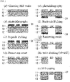
- the scanning mirror according to the embodiment of the present invention can be suitably manufactured by the manufacturing method for the scanning mirror according to an embodiment of the present invention. That is, as illustrated in FIG. 2 , in the manufacturing method for the scanning mirror according to the embodiment of the present invention, first, cleaning of a SOI wafer is performed (see FIG. 2(a) ), and a registry polymer 31 is applied to the surface of the device layer 11 of the SOI wafer, and patterning is performed by photolithography using a mask pattern (see FIG. 2(b) ). Etching of the device layer 11 is performed by a deep RIE (Deep RIE) apparatus (see FIG. 2(c) ). After etching, the registry polymer 31 is removed with a stripping solution (see FIG. 2(d) ). As a result, the support electrode 21, the beam portions 22, the connecting bars 23, the mirror portion 24, and the torsion bars 25 are formed on the device layer 11.
- RIE deep RIE
- the registry polymer 31 is applied to the surface of the handle layer 12 of the SOI wafer and patterning is performed by photolithography (see FIG. 2(e) ), and etching of the handle layer 12 is performed by deep RIE (see FIG. 2 (f) ). After that, the registry polymer 31 is removed (see FIG. 2 (g) ). As a result, the application electrodes 26 are formed. Subsequently, the BOX layer 13 in the range of the mirror hole 22a is etched with an etching solution (see FIG. 2(h) ). After that, the ALD layer 27 is formed so as to cover the entire exposed surface by the atomic layer deposition method (see FIG. 2 (i) ).
- the thickness of the handle layer 12 of the SOI wafer is 200 ⁇ m
- the thickness of the BOX layer 13 is 1 ⁇ m
- the thickness of the device layer 11 is 90 ⁇ m.
- the registry polymer 31 is OFPR 800-LB 200cp.
- the deep RIE apparatus is manufactured by STS, and the etching gas of the deep RIE is SF 6 gas, and the passivation gas is C 4 F 8 gas.
- the stripping solution is "EKC265 (registered trademark)" manufactured by DuPont.
- the etching solution of the BOX layer 13 is an HF solution having a concentration of 49%.
- the ALD layer 27 is made of aluminum oxide (Al 2 O 3 ).
- the scanning mirror according to the embodiment of the present invention can be manufactured as MEMS by a silicon microfabrication technology using the manufacturing method for the scanning mirror according to the embodiment of the present invention.
- the ALD layer 27 can be brought into close contact with the surfaces thereof to cover the irregularities and fine cracks occurring when these components are formed. Further, in the scanning mirror of the embodiment of the present invention, the ALD layer 27 can almost completely prevent moisture and oxygen from adhering to the surfaces of the torsion bar 25, the support electrode 21, and the application electrodes 26.
- the torsional fracture strength of the torsion bar 25 can be increased by the ALD layer 27.
- the scanning mirror since the electrostatic actuator composed of the support electrode 21, the beam portions 22, and the application electrodes 26 has a high amplification function achieved by a machine, the scanning mirror can be driven at a higher speed, a higher scanning angle, and lower power consumption. Further, in the scanning mirror of the embodiment of the present invention, since the ALD layer 27 is made of an aluminum oxide as an insulator, it is possible to prevent a short circuit due to contact between the support electrode 21 and the beam portions 22 and the application electrodes 26 and further extend the movable range of the electrostatic actuator.
- the ALD layer 27 is made of an aluminum oxide, the dielectric constant of the support electrode 21 and the application electrodes 26 can be increased, and the electrostatic force generated by the electrostatic actuator can be increased. Further, by driving the mirror unit 24 at a resonance frequency, the rotation angle of the mirror unit 24 can be further increased.
- the scanning mirror according to the embodiment of the present invention illustrated in FIG. 1 was manufactured by the manufacturing method for the scanning mirror according to the embodiment of the present invention illustrated in FIG. 2 .
- Three types of scanning mirrors in which 10 atomic layers, 400 atomic layers, and 800 atomic layers were formed by the ALD method were manufactured. Theoretically, since one layer is as thick as 1 angstrom (0.1 nm), the thicknesses of the ALD layers 27 of the scanning mirrors are 1 nm, 40 nm, and 80 nm, respectively.
- the length l a of one beam portion 22 is 14,210 ⁇ m
- the width b a of the beam portion 22 is 140 ⁇ m
- the length l c from the connection end between each connecting bar 23 and each beam portion 22 to the connecting portion between each connecting bar 23 and each torsion bar 25 is 500 ⁇ m
- the width b c of each connecting bar 23 is 90 ⁇ m.
- the manufacturing error of the scanning mirror was on the order of 0.1 ⁇ m.
- the resonance frequency was 43.3 Hz
- the displacement of the end of the mirror portion 24 was 1,163 mm
- the optical scanning angle was 0.533 deg.
- the cross-section was observed with a scanning electron microscope (SEM) and the surface roughness was measured with a surface roughness measuring machine (manufactured by Zygo Corporation).
- the residual stress of the scanning mirror having 800 atomic layers was measured by a Raman spectroscope.
- the cross-sectional observation result of the SEM is illustrated in FIG. 3
- the surface shape measurement result is illustrated in FIG. 4
- the residual stress measurement result is illustrated in FIG. 5 .
- the ALD layer 27 (between the circles in the drawing) having a thickness of approximately 80 nm could be confirmed. However, as illustrated in FIGS. 3(b) and 3(c) , the ALD layer 27 could not be clearly confirmed in the scanning mirrors having 10 and 400 atomic layers.
- the scanning mirrors have fine irregularities with a height difference of several nm or less, but it was confirmed that the overall surface irregularities were within the range of approximately 5 nm.
- a scanning mirror in which an ALD layer made of an Al 2 O 3 film was formed was manufactured by the manufacturing method for the scanning mirror according to the embodiment of the present invention illustrated in FIG. 2 .
- the layer thickness of the ALD layer is 2.64 nm.
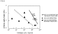
- An experiment was conducted in which a constant stress was repeatedly applied to this scanning mirror using a fatigue test device, and the presence of fracture within the measurement time was examined. The results of the experiment in which the applied stress was changed are plotted in a graph illustrating the relationship between the stress amplitude and the fatigue life (number of repetitions), and are illustrated in FIG. 6 .
- the same experiment was performed on a scanning mirror in which the ALD layer was not formed, and the results are also illustrated in FIG. 6 .
- the data marked with " ⁇ " in FIG. 6 is a scanning mirror that did not fracture within the measurement time, and indicates that the fatigue life is larger than the plotted value. As illustrated in FIG. 6 , it was confirmed that the logarithmic value of the fatigue life decreased as the applied stress amplitude increased. Further, in the stress amplitude region where the scanning mirror illustrated in FIG. 6 is usually used, it was confirmed that the fatigue life of the scanning mirror having the ALD layer was extended by an order of magnitude or more as compared to a scanning mirror having no ALD layer even if the layer thickness is as thin as 2.64 nm.
Landscapes
- Chemical & Material Sciences (AREA)
- Engineering & Computer Science (AREA)
- Physics & Mathematics (AREA)
- Metallurgy (AREA)
- Organic Chemistry (AREA)
- Chemical Kinetics & Catalysis (AREA)
- Materials Engineering (AREA)
- Mechanical Engineering (AREA)
- General Chemical & Material Sciences (AREA)
- Inorganic Chemistry (AREA)
- General Physics & Mathematics (AREA)
- Optics & Photonics (AREA)
- Microelectronics & Electronic Packaging (AREA)
- Computer Hardware Design (AREA)
- Manufacturing & Machinery (AREA)
- Analytical Chemistry (AREA)
- Micromachines (AREA)
- Mechanical Light Control Or Optical Switches (AREA)
- Mechanical Optical Scanning Systems (AREA)
Abstract
Description
- The present invention relates to a scanning mirror and a manufacturing method for the scanning mirror.
- Conventionally, in devices such as laser projectors, laser displays, and OCT probes equipped with optical coherence tomography (OCT) functions, those using a MEMS (Micro Electro Mechanical Systems) microscanner manufactured by a microfabrication technology have been developed in order to reduce the size and facilitate portability (see, for example,
Patent Literatures 1 to 4). This microscanner has a scanning mirror which includes a mirror portion that reflects a laser beam and a torsion bar that supports the mirror portion, and which applies a torsional force to the torsion bar to rotate the mirror portion to scan the laser beam two-dimensionally. - In order to improve the performance of such a MEMS microscanner, it is necessary to drive the scanning mirror at a higher speed, a higher scanning angle, and lower power consumption. Therefore, a PZT (lead-zirconate-titanate)-driven microscanner in which the rotation angle of a mirror portion is increased by a high amplification function achieved by a machine which is a combination of a torsion bar and a cantilever has been developed (see, for example, Non-Patent
Literature 1 or 2). - Further, in order to increase the torsional fracture strength of a torsion bar to improve the durability, a structure in which the surface of a mirror portion and the torsion bar is covered with a diamond-like carbon (DLC) film using plasma CVD (plasma enhanced chemical vapor deposition) has been proposed (see Non-Patent Literature 3). According to this structure, the torsional fracture strength can be improved by 11.1% to 30.0%.
- Researches have been conducted to examine the effects of an aluminum oxide (Al2O3) layer formed on the surface of a polycrystalline silicon film or the surface of a polymer layer using an atomic layer deposition (ALD) method (see, for example,
Non-Patent Literature 4 or 5). However, in these researches, an aluminum oxide layer is not formed on the surface of a torsion bar of a scanning mirror. -
- Patent Literature 1:
Japanese Patent No. 3934578 - Patent Literature 2:
Japanese Patent No. 5321740 - Patent Literature 3:
Japanese Patent No. 5640420 - Patent Literature 4:
Japanese Patent No. 6018926 - Non-Patent Literature 1: S. Gu-Stoppel, D. Kaden, H. J. Quenzer, U. Hofmann, W. Benecke, "High speed piezoelectric microscanners with large deflection using mechanical leverage amplification", Procedia Engineering, 2012, 47, p. 56-59
- Non-Patent Literature 2: S. Gu-Stoppel, T. Giese, H. J. Quenzer, U. Hofmann, W. Benecke, "PZT-Actuated and -Sensed Resonant Micromirrors with Large Scan Angles Applying Mechanical Leverage Amplification for Biaxial Scanning", Micromachines, 2017, 8, 215
- Non-Patent Literature 3: W. Zhang, K. Obitani, Y. Hirai, T. Tsuchiya, O. Tabata, "Fracture strength of silicon torsional mirror resonators fully coated with submicrometer-thick PECVD DLC film", Sensors and Actuators A: Physical, 2019, 286, p. 28-34
- Non-Patent Literature 4: M. Budnitzki, O. Pierron, "The influence of nanoscale atomic-layer-deposited alumina coating on the fatigue behavior of polycrystalline silicon thin films", Applied Physics Letters, 2009, 94, 141906
- Non-Patent Literature 5: P. F. Carcia, R. S. McLean, M. H. Reilly, "Permeation measurements and modeling of highly defective Al2O3 thin films grown by atomic layer deposition on polymers", Applied Physics Letters, 2010, 97, 221901
- In conventional scanning mirrors as described in
Patent Literatures 1 to 4 andNon-Patent Literatures Literature 3, since a DLC film is formed on the surface of the torsion bar, the progress of oxidation and hydroxylation of the torsion bar can be delayed. However, since plasma CVD is used for forming the DLC film, there is a problem that the adhesion of water and oxygen to the surface of the torsion bar cannot be completely prevented, and the deterioration of the torsion bar cannot be suppressed. - The present invention has been made in view of such a problem, and an object thereof is to provide a scanning mirror and a manufacturing method for the scanning mirror capable of preventing oxidation and hydroxylation of a torsion bar, thereby suppressing deterioration of the torsion bar.
- In order to achieve the above object, a scanning mirror according to the present invention includes a mirror portion; and a torsion bar provided so as to support the mirror portion and of which the surface is covered with an ALD layer, wherein the scanning mirror is configured such that the mirror portion can be rotated around an axis extending along the torsion bar when torsional force is applied to the torsion bar.
- In the scanning mirror according to the present invention, since the surface of the torsion bar is covered with the ALD layer, the ALD layer can be brought into close contact with the surface of the torsion bar to cover irregularities and fine cracks occurring when the torsion bar is formed. Further, since the ALD layer is formed by an atomic layer deposition (ALD) method, the ALD layer is denser than a deposition layer by plasma CVD and has no pinholes. Therefore, in the scanning mirror according to the present invention, the ALD layer can almost completely prevent moisture and oxygen from adhering to the surface of the torsion bar. As a result, oxidation and hydroxylation of the torsion bar can be prevented, whereby deterioration of the torsion bar can be suppressed. Further, in the scanning mirror according to the present invention, the torsional fracture strength of the torsion bar can be increased by the ALD layer.
- The scanning mirror according to the present invention preferably has an electrostatic actuator having a pair of electrodes of which the surface is covered with the ALD layer, the electrostatic actuator being provided to be deformable so that torsional force is applied to the torsion bar when a voltage is applied between the electrodes. In this case, the ALD film can prevent the oxidation and hydroxylation of the electrodes as well as the torsion bar, whereby the deterioration of the electrodes can be suppressed. Further, by configuring the electrostatic actuator to have a high amplification function achieved by a machine, the scanning mirror can be driven at a higher speed, a higher scanning angle, and lower power consumption.
- A manufacturing method for a scanning mirror according to the present invention is a manufacturing method for a scanning mirror configured such that a mirror portion can be rotated around an axis extending along a torsion bar when torsional force is applied to the torsion bar provided so as to support the mirror portion, the manufacturing method comprising: forming the ALD layer on a surface of the torsion bar by an atomic layer deposition method after the mirror portion and the torsion bar are formed.
- The manufacturing method for the scanning mirror according to the present invention can suitably manufacture the scanning mirror according to the present invention. In the manufacturing method for a scanning mirror according to the present invention, since the ALD layer is formed on the surface of the torsion bar by an atomic layer deposition method, the formed ALD layer can make close contact with the surface of the torsion bar to cover irregularities and fine cracks occurring when the torsion bar is formed. In the manufacturing method for a scanning mirror according to the present invention, the formed ALD layer can almost completely prevent moisture and oxygen from adhering to the surface of the torsion bar. As a result, oxidation and hydroxylation of the torsion bar can be prevented, whereby deterioration of the torsion bar can be suppressed. Further, the formed ALD layer can increase the torsional fracture strength of the torsion bar.
- In the manufacturing method for the scanning mirror according to the present invention, the scanning mirror may have an electrostatic actuator provided to be deformable so that torsional force is applied to the torsion bar when a voltage is applied between a pair of electrodes, and the ALD layer may be formed at least on a surface of the torsion bar and surfaces of the electrodes of the electrostatic actuator by an atomic layer deposition method after the mirror portion, the torsion bar, and the electrostatic actuator are formed. In this case, the formed ALD film can prevent the oxidation and hydroxylation of the electrodes as well as the torsion bar, whereby the deterioration of the electrodes can be suppressed. Further, by forming an electrostatic actuator having a high amplification function achieved by a machine, it is possible to manufacture a scanning mirror that can be driven at a higher speed, a higher scanning angle, and lower power consumption.
- In the scanning mirror and the manufacturing method for the scanning mirror according to the present invention, the ALD layer may be made of any material as long as it enhances the strength of the torsion bar against fatigue, and for example, may be made of any one or more of an aluminum oxide (Al2O3), an aluminum nitride (AlN), a silicon nitride (Si3N4), a silicon carbide (SiC), a gallium nitride (GaN). Further, the ALD layer may be made of an insulator. In this case, by covering the electrodes of the electrostatic actuator with the ALD layer, a short circuit due to contact between the electrodes can be prevented, and the movable range of the electrostatic actuator can be extended. Further, when the ALD layer is made of an aluminum oxide which is an insulator, the dielectric constant of each electrode can be increased, and the electrostatic force generated by the electrostatic actuator can be increased.
- In the scanning mirror and the manufacturing method for the scanning mirror according to the present invention, it is preferable that the mirror portion and the torsion bar are made of silicon (Si). Further, when the scanning mirror has an electrostatic actuator, it is preferable that the electrostatic actuator is also made of silicon. In particular, in the scanning mirror according to the present invention, it is preferable that the scanning mirror is MEMS manufactured by silicon microfabrication technology. Further, in the manufacturing method for the scanning mirror according to the present invention, it is preferable to manufacture the scanning mirror by a silicon microfabrication technology.
- In the scanning mirror and the manufacturing method for the scanning mirror according to the present invention, the ALD layer preferably has a thickness of 0.5 nm to 200 nm. In this case, deterioration of the torsion bar and the electrodes can be suppressed without hindering the movement of the torsion bar.
- According to the present invention, it is possible to provide a scanning mirror and a manufacturing method for the scanning mirror capable of preventing oxidation and hydroxylation of a torsion bar, thereby suppressing deterioration of the torsion bar.
-
-
FIG. 1 is a plan view illustrating each portion of a scanning mirror according to an embodiment of the present invention, in which (a) illustrates a mirror portion formed by processing a device layer and (b) illustrates application electrodes formed by processing a handle layer. -
FIG. 2 is a side view illustrating a manufacturing method for the scanning mirror according to the embodiment of the present invention. -
FIG. 3 illustrates scanning electron microscope (SEM) photographs of cross-sections of the scanning mirror according to the embodiment of the present invention when (a) 800 layers, (b) 400 layers, and (c) 10 layers of atomic layers are deposited by an ALD method. -
FIG. 4 is a graph illustrating the measurement results of the surface shape of the scanning mirror according to the embodiment of the present invention when 800 layers, 400 layers, and 10 atomic layers are deposited by the ALD method, and the surface shape of the atomic layers before the deposition. -
FIG. 5 is a graph illustrating a measurement result of residual stress when 800 atomic layers of the scanning mirror according to the embodiment of the present invention are deposited by the ALD method. -
FIG. 6 is a graph illustrating the relationship between stress amplitude and fatigue life of a scanning mirror (with ALD deposition) according to the embodiment of the present invention and a scanning mirror without ALD deposition, which is a comparative example. - Hereinafter, an embodiment of the present invention will be described with reference to the drawings.
-
FIGS. 1 to 6 illustrate a scanning mirror and a manufacturing method for the scanning mirror according to an embodiment of the present invention. - The scanning mirror according to the embodiment of the present invention is manufactured using an SOI (Silicon on Insulator) wafer having a BOX layer made of SiO2 between a handle layer made of Si and a device layer. In the SOI wafer, the handle layer and the device layer are insulated by the BOX layer.
- As illustrated in
FIG. 1 , the scanning mirror according to the embodiment of the present invention includes asupport electrode 21, fourbeam portions 22, two connectingbars 23, amirror portion 24, twotorsion bars 25, and twoapplication electrodes 26. Thesupport electrode 21, thebeam portions 22, the connectingbars 23, themirror portion 24, and the torsion bars 25 are formed by processing thedevice layer 11. Theapplication electrodes 26 are formed by processing thehandle layer 12. - As illustrated in
FIG. 1(a) , thesupport electrode 21 has a rectangular frame shape. The fourbeam portions 22 each are formed so that a plurality of elongated rectangular plates are arranged side by side in parallel in the width direction, and the rectangular plates are alternately connected to both neighboring rectangular plates at different ends. Thebeam portions 22 are arranged so that twobeam portions 22 are arranged side by side along a pair of long sides of a rectangular inner edge 21a of thesupport electrode 21, and the twobeam portions 22 extend up to ends on different sides from the central portions of the corresponding long sides to be arranged with a gap between the beam portions and the corresponding long sides. Thebeam portions 22 are arranged so that an elongatedrectangular mirror hole 22a is formed between two beam portions arranged along one long side and two beam portions arranged along the other long side. Further, thebeam portions 22 are arranged so that the rectangular plates are parallel to the short side of the inner edge 21a of thesupport electrode 21, and are connected to thesupport electrode 21 on the central portion side of the long side of the inner edge 21a. - The two connecting
bars 23 are provided so as to connect thebeam portions 22 facing each other with themirror hole 22a interposed therebetween on one short side and the other short side of the inner edge 21a of thesupport electrode 21, respectively. The connecting bars 23 connect thebeam portions 22 to each other on each short side of the inner edge 21a. Themirror portion 24 has a disk shape and is arranged in the central portion of themirror hole 22a so as not to come into contact with thebeam portions 22. The twotorsion bars 25 are parallel to each long side of the inner edge 21a of thesupport electrode 21, and are each provided so as to connect the central portion of each connectingbar 23 and themirror portion 24. As a result, the torsion bars 25 support themirror portion 24. - As illustrated in
FIG. 1(a) , thesupport electrode 21, thebeam portions 22, the connectingbars 23, themirror portion 24, and the torsion bars 25 have a shape that is bilaterally symmetrical with respect to the center line parallel to each long side of the inner edge 21a of thesupport electrode 21 and is also bilaterally symmetrical with respect to the center line parallel to each short side of the inner edge 21a of thesupport electrode 21. - As illustrated in
FIG. 1(b) , theapplication electrodes 26 are provided in portions facing thesupport electrode 21 and thebeam portions 22, and arectangular drive hole 26a corresponding to themirror hole 22a is formed at the center thereof. One of theapplication electrodes 26 is provided so as to face a region on one long side of the inner edge 21a of thesupport electrode 21, twobeam portions 22 along the long side thereof, and a region on one short side of the inner edge 21a of thesupport electrode 21. Theother application electrode 26 is provided so as to face a region on the other long side of the inner edge 21a of thesupport electrode 21, twobeam portions 22 along the long side thereof, and a region on the other short side of the inner edge 21a of thesupport electrode 21. Theapplication electrodes 26 are not electrically connected. - In the scanning mirror according to the embodiment of the present invention, the
support electrode 21, thebeam portions 22, the connectingbars 23, themirror portion 24, and the torsion bars 25 formed on thedevice layer 11 and theapplication electrodes 26 formed on the handle layers 12 are arranged at intervals by the BOX layer and are insulated by the BOX layer. In the scanning mirror according to the embodiment of the present invention, thesupport electrode 21, thebeam portions 22, and theapplication electrodes 26 form an electrostatic actuator. - In the scanning mirror according to the embodiment of the present invention, the surfaces of the
support electrode 21, thebeam portions 22, the connectingbars 23, themirror portion 24, the torsion bars 25, and theapplication electrodes 26 are covered with an ALD layer. In a specific example illustrated inFIG. 1 , although the ALD layer is made of an aluminum oxide (Al2O3) which is an insulator, the ALD layer may be made of an aluminum nitride (AlN), a silicon nitride (Si3N4), a silicon carbide (SiC), a gallium nitride (GaN), or the like in addition to aluminum oxide (Al2O3). - As illustrated in
FIG. 1 , the scanning mirror according to the embodiment of the present invention is configured such that themirror portion 24 can be rotated as follows. That is, by grounding thesupport electrode 21 and applying an AC voltage shifted in phase by π to theapplication electrodes 26, thebeam portion 22 facing oneapplication electrode 26 and thebeam portion 22 facing theother application electrode 26 are deformed with a phase shift of π. As a result, the connectingbars 23 are similarly deformed, and a torsional force in the same direction is applied to the torsion bars 25. Due to this torsional force, themirror portion 24 is rotated inside themirror hole 22a and thedrive hole 26a around the axis along the torsion bars 25. - The scanning mirror according to the embodiment of the present invention can be suitably manufactured by the manufacturing method for the scanning mirror according to an embodiment of the present invention. That is, as illustrated in
FIG. 2 , in the manufacturing method for the scanning mirror according to the embodiment of the present invention, first, cleaning of a SOI wafer is performed (seeFIG. 2(a) ), and aregistry polymer 31 is applied to the surface of thedevice layer 11 of the SOI wafer, and patterning is performed by photolithography using a mask pattern (seeFIG. 2(b) ). Etching of thedevice layer 11 is performed by a deep RIE (Deep RIE) apparatus (seeFIG. 2(c) ). After etching, theregistry polymer 31 is removed with a stripping solution (seeFIG. 2(d) ). As a result, thesupport electrode 21, thebeam portions 22, the connectingbars 23, themirror portion 24, and the torsion bars 25 are formed on thedevice layer 11. - Subsequently, in the same manner, the
registry polymer 31 is applied to the surface of thehandle layer 12 of the SOI wafer and patterning is performed by photolithography (seeFIG. 2(e) ), and etching of thehandle layer 12 is performed by deep RIE (seeFIG. 2 (f) ). After that, theregistry polymer 31 is removed (seeFIG. 2 (g) ). As a result, theapplication electrodes 26 are formed. Subsequently, theBOX layer 13 in the range of themirror hole 22a is etched with an etching solution (seeFIG. 2(h) ). After that, theALD layer 27 is formed so as to cover the entire exposed surface by the atomic layer deposition method (seeFIG. 2 (i) ). - In a specific example illustrated in
FIG. 2 , the thickness of thehandle layer 12 of the SOI wafer is 200 µm, the thickness of theBOX layer 13 is 1 µm, and the thickness of thedevice layer 11 is 90 µm. Theregistry polymer 31 is OFPR 800-LB 200cp. The deep RIE apparatus is manufactured by STS, and the etching gas of the deep RIE is SF6 gas, and the passivation gas is C4F8 gas. The stripping solution is "EKC265 (registered trademark)" manufactured by DuPont. The etching solution of theBOX layer 13 is an HF solution having a concentration of 49%. TheALD layer 27 is made of aluminum oxide (Al2O3). - As described above, the scanning mirror according to the embodiment of the present invention can be manufactured as MEMS by a silicon microfabrication technology using the manufacturing method for the scanning mirror according to the embodiment of the present invention. In the scanning mirror of the embodiment of the present invention, since the surfaces of the
torsion bar 25, thesupport electrode 21, and theapplication electrodes 26 are covered with theALD layer 27, theALD layer 27 can be brought into close contact with the surfaces thereof to cover the irregularities and fine cracks occurring when these components are formed. Further, in the scanning mirror of the embodiment of the present invention, theALD layer 27 can almost completely prevent moisture and oxygen from adhering to the surfaces of thetorsion bar 25, thesupport electrode 21, and theapplication electrodes 26. As a result, oxidation and hydroxylation of thetorsion bar 25, thesupport electrode 21, and theapplication electrodes 26 can be prevented, and deterioration thereof can be suppressed. Further, in the scanning mirror according to the embodiment of the present invention, the torsional fracture strength of thetorsion bar 25 can be increased by theALD layer 27. - In the scanning mirror according to the embodiment of the present invention, since the electrostatic actuator composed of the
support electrode 21, thebeam portions 22, and theapplication electrodes 26 has a high amplification function achieved by a machine, the scanning mirror can be driven at a higher speed, a higher scanning angle, and lower power consumption. Further, in the scanning mirror of the embodiment of the present invention, since theALD layer 27 is made of an aluminum oxide as an insulator, it is possible to prevent a short circuit due to contact between thesupport electrode 21 and thebeam portions 22 and theapplication electrodes 26 and further extend the movable range of the electrostatic actuator. Further, since theALD layer 27 is made of an aluminum oxide, the dielectric constant of thesupport electrode 21 and theapplication electrodes 26 can be increased, and the electrostatic force generated by the electrostatic actuator can be increased. Further, by driving themirror unit 24 at a resonance frequency, the rotation angle of themirror unit 24 can be further increased. - The scanning mirror according to the embodiment of the present invention illustrated in
FIG. 1 was manufactured by the manufacturing method for the scanning mirror according to the embodiment of the present invention illustrated inFIG. 2 . Three types of scanning mirrors in which 10 atomic layers, 400 atomic layers, and 800 atomic layers were formed by the ALD method were manufactured. Theoretically, since one layer is as thick as 1 angstrom (0.1 nm), the thicknesses of the ALD layers 27 of the scanning mirrors are 1 nm, 40 nm, and 80 nm, respectively. Further, in each of the manufactured scanning mirrors, the length la of onebeam portion 22 is 14,210 µm, the width ba of thebeam portion 22 is 140 µm, the length lc from the connection end between each connectingbar 23 and eachbeam portion 22 to the connecting portion between each connectingbar 23 and eachtorsion bar 25 is 500 µm, and the width bc of each connectingbar 23 is 90 µm. - The manufacturing error of the scanning mirror was on the order of 0.1 µm. When the scanning mirror before the formation of the
ALD layer 27 was measured by LVD (Laser Doppler Vibrometer; manufactured by Polytech), the resonance frequency was 43.3 Hz, the displacement of the end of themirror portion 24 was 1,163 mm, and the optical scanning angle was 0.533 deg. - For the three types of manufactured scanning mirrors, the cross-section was observed with a scanning electron microscope (SEM) and the surface roughness was measured with a surface roughness measuring machine (manufactured by Zygo Corporation). In addition, the residual stress of the scanning mirror having 800 atomic layers was measured by a Raman spectroscope. The cross-sectional observation result of the SEM is illustrated in
FIG. 3 , the surface shape measurement result is illustrated inFIG. 4 , and the residual stress measurement result is illustrated inFIG. 5 . - As illustrated in
FIG. 3(a) , in the scanning mirror having 800 atomic layers, the ALD layer 27 (between the circles in the drawing) having a thickness of approximately 80 nm could be confirmed. However, as illustrated inFIGS. 3(b) and 3(c) , theALD layer 27 could not be clearly confirmed in the scanning mirrors having 10 and 400 atomic layers. - As illustrated in
FIG. 4 , the scanning mirrors have fine irregularities with a height difference of several nm or less, but it was confirmed that the overall surface irregularities were within the range of approximately 5 nm. When the arithmetic mean roughness Ra of the surface roughness of each scanning mirror was obtained from these surface shapes, the scanning mirror having 800 atomic layers had Ra = 0.00066, the scanning mirror having 400 atomic layers had Ra = 0.00068, and the scanning mirror having 10 atomic layers had Ra = 0.007796. From this result, it was confirmed that the thicker theALD layer 27, the smaller the surface roughness and the more flat it became. Note thatFIG. 4 also illustrates the surface shape of the scanning mirror before deposition of the atomic layer as a comparative example, and the arithmetic mean roughness thereof was Ra = 0.00042. - As illustrated in
FIG. 5 , it was confirmed that the residual stress was distributed in the scanning mirror having 800 atomic layers. It is considered that this residual stress was generated due to the temperature difference when the atomic layer was formed by the ALD method. - A scanning mirror in which an ALD layer made of an Al2O3 film was formed was manufactured by the manufacturing method for the scanning mirror according to the embodiment of the present invention illustrated in
FIG. 2 . The layer thickness of the ALD layer is 2.64 nm. An experiment was conducted in which a constant stress was repeatedly applied to this scanning mirror using a fatigue test device, and the presence of fracture within the measurement time was examined. The results of the experiment in which the applied stress was changed are plotted in a graph illustrating the relationship between the stress amplitude and the fatigue life (number of repetitions), and are illustrated inFIG. 6 . For comparison, the same experiment was performed on a scanning mirror in which the ALD layer was not formed, and the results are also illustrated inFIG. 6 . - The data marked with "→" in
FIG. 6 is a scanning mirror that did not fracture within the measurement time, and indicates that the fatigue life is larger than the plotted value. As illustrated inFIG. 6 , it was confirmed that the logarithmic value of the fatigue life decreased as the applied stress amplitude increased. Further, in the stress amplitude region where the scanning mirror illustrated inFIG. 6 is usually used, it was confirmed that the fatigue life of the scanning mirror having the ALD layer was extended by an order of magnitude or more as compared to a scanning mirror having no ALD layer even if the layer thickness is as thin as 2.64 nm. -
- 11 Device layer
- 12 Handle layer
- 13 BOX layer
- 21 Support electrode
- 21a Inner edge
- 22 Beam portion
- 22a Mirror hole
- 23 Connecting bar
- 24 Mirror portion
- 25 Torsion bar
- 26 Application electrode
- 26a Drive hole
- 27 ALD layer
- 31 Registry polymer
Claims (8)
- A scanning mirror comprising:a mirror portion; anda torsion bar provided so as to support the mirror portion and of which the surface is covered with an ALD layer, whereinthe scanning mirror is configured such that the mirror portion can be rotated around an axis extending along the torsion bar when torsional force is applied to the torsion bar.
- The scanning mirror according to claim 1, further comprising:
an electrostatic actuator having a pair of electrodes of which the surface is covered with the ALD layer, the electrostatic actuator being provided to be deformable so that torsional force is applied to the torsion bar when a voltage is applied between the electrodes. - The scanning mirror according to claim 1 or 2, wherein
the ALD layer is made of an insulator. - The scanning mirror according to any one of claims 1 to 3, wherein
the ALD layer is made of any one or more of an aluminum oxide (Al2O3), an aluminum nitride (AlN), a silicon nitride (Si3N4), a silicon carbide (SiC), a gallium nitride (GaN). - The scanning mirror according to any one of claims 1 to 4, wherein
the mirror portion and the torsion bar are made of silicon (Si). - The scanning mirror according to any one of claims 1 to 5, wherein
the ALD layer has a thickness of 0.5 nm to 200 nm. - A manufacturing method for a scanning mirror configured such that a mirror portion can be rotated around an axis extending along a torsion bar when torsional force is applied to the torsion bar provided so as to support the mirror portion, the manufacturing method comprising:
forming the ALD layer at least on a surface of the torsion bar by an atomic layer deposition method after the mirror portion and the torsion bar are formed. - The manufacturing method for the scanning mirror according to claim 7, whereinthe scanning mirror has an electrostatic actuator provided to be deformable so that torsional force is applied to the torsion bar when a voltage is applied between a pair of electrodes, andthe ALD layer is formed at least on a surface of the torsion bar and surfaces of the electrodes of the electrostatic actuator by an atomic layer deposition method after the mirror portion, the torsion bar, and the electrostatic actuator are formed.
Applications Claiming Priority (2)
| Application Number | Priority Date | Filing Date | Title |
|---|---|---|---|
| JP2019098158 | 2019-05-25 | ||
| PCT/JP2020/018008 WO2020241153A1 (en) | 2019-05-25 | 2020-04-27 | Scanning mirror and production method for scanning mirror |
Publications (2)
| Publication Number | Publication Date |
|---|---|
| EP3978987A1 true EP3978987A1 (en) | 2022-04-06 |
| EP3978987A4 EP3978987A4 (en) | 2022-07-27 |
Family
ID=73552548
Family Applications (1)
| Application Number | Title | Priority Date | Filing Date |
|---|---|---|---|
| EP20814367.7A Withdrawn EP3978987A4 (en) | 2019-05-25 | 2020-04-27 | SCAN MIRROR AND METHOD FOR PRODUCING THE SCAN MIRROR |
Country Status (5)
| Country | Link |
|---|---|
| US (1) | US12298494B2 (en) |
| EP (1) | EP3978987A4 (en) |
| JP (1) | JP6795165B1 (en) |
| CN (1) | CN113227874A (en) |
| WO (1) | WO2020241153A1 (en) |
Families Citing this family (1)
| Publication number | Priority date | Publication date | Assignee | Title |
|---|---|---|---|---|
| CN120553632A (en) * | 2024-11-29 | 2025-08-29 | 比亚迪股份有限公司 | A MEMS micromirror, optical device and terminal equipment |
Family Cites Families (17)
| Publication number | Priority date | Publication date | Assignee | Title |
|---|---|---|---|---|
| GB1290252A (en) | 1970-03-26 | 1972-09-27 | ||
| JPS512073A (en) | 1974-06-24 | 1976-01-09 | Jinji Furuse | TANZOKI |
| JPS6018926B2 (en) | 1978-08-12 | 1985-05-13 | 岩崎通信機株式会社 | Optical signal observation device |
| JP4514075B2 (en) * | 2000-07-25 | 2010-07-28 | シチズンファインテックミヨタ株式会社 | Galvano device manufacturing method and galvano device |
| JP3827977B2 (en) * | 2001-08-20 | 2006-09-27 | 富士通株式会社 | Manufacturing method of micromirror element |
| US7553686B2 (en) * | 2002-12-17 | 2009-06-30 | The Regents Of The University Of Colorado, A Body Corporate | Al2O3 atomic layer deposition to enhance the deposition of hydrophobic or hydrophilic coatings on micro-electromechanical devices |
| JP3934578B2 (en) | 2003-06-09 | 2007-06-20 | ペンタックス株式会社 | Scanning mirror, beam scanning probe |
| US20070211257A1 (en) | 2006-03-09 | 2007-09-13 | Kearl Daniel A | Fabry-Perot Interferometer Composite and Method |
| JP2008168438A (en) * | 2007-01-09 | 2008-07-24 | Seiko Epson Corp | Electrostatic actuator, droplet discharge head, manufacturing method thereof, and droplet discharge apparatus |
| JP5640420B2 (en) | 2009-05-29 | 2014-12-17 | 株式会社リコー | Projection-type image display device |
| WO2011142210A1 (en) | 2010-05-12 | 2011-11-17 | コニカミノルタオプト株式会社 | Scanning optical system and projector provided with same |
| US8771807B2 (en) * | 2011-05-24 | 2014-07-08 | Air Products And Chemicals, Inc. | Organoaminosilane precursors and methods for making and using same |
| JP6018926B2 (en) | 2013-01-09 | 2016-11-02 | 富士フイルム株式会社 | Micromirror device and manufacturing method thereof |
| JP6459392B2 (en) * | 2014-10-28 | 2019-01-30 | ミツミ電機株式会社 | Optical scanning device |
| WO2017006425A1 (en) * | 2015-07-07 | 2017-01-12 | 富士通株式会社 | Optical device |
| JP2017102232A (en) * | 2015-12-01 | 2017-06-08 | セイコーエプソン株式会社 | Optical device, image display device, and head mount display |
| US10029908B1 (en) * | 2016-12-30 | 2018-07-24 | Texas Instruments Incorporated | Dielectric cladding of microelectromechanical systems (MEMS) elements for improved reliability |
-
2020
- 2020-04-27 JP JP2020545752A patent/JP6795165B1/en active Active
- 2020-04-27 EP EP20814367.7A patent/EP3978987A4/en not_active Withdrawn
- 2020-04-27 US US17/417,981 patent/US12298494B2/en active Active
- 2020-04-27 WO PCT/JP2020/018008 patent/WO2020241153A1/en not_active Ceased
- 2020-04-27 CN CN202080007573.0A patent/CN113227874A/en active Pending
Also Published As
| Publication number | Publication date |
|---|---|
| EP3978987A4 (en) | 2022-07-27 |
| US20220066198A1 (en) | 2022-03-03 |
| US12298494B2 (en) | 2025-05-13 |
| JP6795165B1 (en) | 2020-12-02 |
| CN113227874A (en) | 2021-08-06 |
| WO2020241153A1 (en) | 2020-12-03 |
| JPWO2020241153A1 (en) | 2021-09-13 |
Similar Documents
| Publication | Publication Date | Title |
|---|---|---|
| US11950052B2 (en) | Acoustic transducer with gap-controlling geometry and method of manufacturing an acoustic transducer | |
| US8409900B2 (en) | Fabricating MEMS composite transducer including compliant membrane | |
| EP3203298B1 (en) | Mirror drive device and drive method therefor | |
| US8426235B2 (en) | Method for manufacturing capacitive electromechanical transducer | |
| KR20140005780A (en) | Capacitive transducer, capacitive transducer manufacturing method, and object information acquisition apparatus | |
| Kobayashi et al. | Fabrication of optical micro scanner driven by PZT actuators | |
| EP2952853B1 (en) | Angular velocity sensor and manufacturing method therefor | |
| US20190366382A1 (en) | Capacitive micromachined ultrasonic transducer and manufacturing method thereof | |
| US20130154440A1 (en) | In-plane actuated resonant device and method of manufacturing the device | |
| Piot et al. | Dual-axis resonant scanning mems mirror with pulsed-laser-deposited barium-doped PZT | |
| WO2015005193A1 (en) | Substrate for diaphragm-type resonant mems devices, diaphragm-type resonant mems device and method for manufacturing same | |
| US12298494B2 (en) | Scanning mirror and manufacturing method for scanning mirror | |
| WO2012145278A2 (en) | Mems composite transducer including compliant membrane | |
| Kanda et al. | Three-dimensional piezoelectric MEMS actuator by using sputtering deposition of Pb (Zr, Ti) O3 on microstructure sidewalls | |
| US11584639B2 (en) | Method for manufacturing a plurality of resonators | |
| Chen et al. | E-beam evaporated polysilicon for lead zirconate titanate-based micro-actuators | |
| JP5453791B2 (en) | Piezoelectric element, manufacturing method thereof, and angular velocity sensor using the piezoelectric element | |
| JP2009198493A (en) | Angular velocity detection device | |
| Lin et al. | Wafer level demonstration and characterization of c-axis oriented Sc 0.3 Al 0.7 N bilayer stacks | |
| US10707405B2 (en) | Electromechanical actuator | |
| JP2001001300A (en) | Fine beam structure and manufacturing method thereof | |
| Mortet et al. | AlN on nanocrystalline diamond piezoelectric cantilevers for sensors/actuators | |
| Faizan et al. | Acoustic Actuation of Suspended Graphene For Linear Excitation of 2D NEMS | |
| JP6577653B2 (en) | Ultrasonic probe and manufacturing method thereof | |
| EP4684614B1 (en) | Method for manufacturing piezoelectric microelectromechanical device |
Legal Events
| Date | Code | Title | Description |
|---|---|---|---|
| STAA | Information on the status of an ep patent application or granted ep patent |
Free format text: STATUS: THE INTERNATIONAL PUBLICATION HAS BEEN MADE |
|
| PUAI | Public reference made under article 153(3) epc to a published international application that has entered the european phase |
Free format text: ORIGINAL CODE: 0009012 |
|
| STAA | Information on the status of an ep patent application or granted ep patent |
Free format text: STATUS: REQUEST FOR EXAMINATION WAS MADE |
|
| 17P | Request for examination filed |
Effective date: 20210818 |
|
| AK | Designated contracting states |
Kind code of ref document: A1 Designated state(s): AL AT BE BG CH CY CZ DE DK EE ES FI FR GB GR HR HU IE IS IT LI LT LU LV MC MK MT NL NO PL PT RO RS SE SI SK SM TR |
|
| A4 | Supplementary search report drawn up and despatched |
Effective date: 20220624 |
|
| RIC1 | Information provided on ipc code assigned before grant |
Ipc: C23C 16/455 20060101ALI20220620BHEP Ipc: C23C 16/40 20060101ALI20220620BHEP Ipc: B81C 1/00 20060101ALI20220620BHEP Ipc: B81B 7/00 20060101ALI20220620BHEP Ipc: B81B 3/00 20060101ALI20220620BHEP Ipc: G02B 26/08 20060101AFI20220620BHEP |
|
| DAV | Request for validation of the european patent (deleted) | ||
| DAX | Request for extension of the european patent (deleted) | ||
| STAA | Information on the status of an ep patent application or granted ep patent |
Free format text: STATUS: THE APPLICATION HAS BEEN WITHDRAWN |
|
| 18W | Application withdrawn |
Effective date: 20240625 |