EP3975405B1 - Schaltsteuerungskreis, multiplexerschaltkreis und steuerungsverfahren für multiplexerschaltsteuerungskreis - Google Patents
Schaltsteuerungskreis, multiplexerschaltkreis und steuerungsverfahren für multiplexerschaltsteuerungskreis Download PDFInfo
- Publication number
- EP3975405B1 EP3975405B1 EP20913988.0A EP20913988A EP3975405B1 EP 3975405 B1 EP3975405 B1 EP 3975405B1 EP 20913988 A EP20913988 A EP 20913988A EP 3975405 B1 EP3975405 B1 EP 3975405B1
- Authority
- EP
- European Patent Office
- Prior art keywords
- switch
- control
- turned
- capacitor
- effect transistor
- Prior art date
- Legal status (The legal status is an assumption and is not a legal conclusion. Google has not performed a legal analysis and makes no representation as to the accuracy of the status listed.)
- Active
Links
Images


Classifications
-
- H—ELECTRICITY
- H03—ELECTRONIC CIRCUITRY
- H03K—PULSE TECHNIQUE
- H03K17/00—Electronic switching or gating, i.e. not by contact-making and –breaking
- H03K17/51—Electronic switching or gating, i.e. not by contact-making and –breaking characterised by the components used
- H03K17/56—Electronic switching or gating, i.e. not by contact-making and –breaking characterised by the components used by the use, as active elements, of semiconductor devices
- H03K17/687—Electronic switching or gating, i.e. not by contact-making and –breaking characterised by the components used by the use, as active elements, of semiconductor devices the devices being field-effect transistors
- H03K17/693—Switching arrangements with several input- or output-terminals, e.g. multiplexers, distributors
-
- H—ELECTRICITY
- H02—GENERATION; CONVERSION OR DISTRIBUTION OF ELECTRIC POWER
- H02M—APPARATUS FOR CONVERSION BETWEEN AC AND AC, BETWEEN AC AND DC, OR BETWEEN DC AND DC, AND FOR USE WITH MAINS OR SIMILAR POWER SUPPLY SYSTEMS; CONVERSION OF DC OR AC INPUT POWER INTO SURGE OUTPUT POWER; CONTROL OR REGULATION THEREOF
- H02M3/00—Conversion of DC power input into DC power output
- H02M3/02—Conversion of DC power input into DC power output without intermediate conversion into AC
- H02M3/04—Conversion of DC power input into DC power output without intermediate conversion into AC by static converters
- H02M3/06—Conversion of DC power input into DC power output without intermediate conversion into AC by static converters using resistors or capacitors, e.g. potential divider
- H02M3/07—Conversion of DC power input into DC power output without intermediate conversion into AC by static converters using resistors or capacitors, e.g. potential divider using capacitors charged and discharged alternately by semiconductor devices with control electrode, e.g. charge pumps
-
- H—ELECTRICITY
- H03—ELECTRONIC CIRCUITRY
- H03F—AMPLIFIERS
- H03F1/00—Details of amplifiers with only discharge tubes, only semiconductor devices or only unspecified devices as amplifying elements
- H03F1/02—Modifications of amplifiers to raise the efficiency, e.g. gliding Class A stages, use of an auxiliary oscillation
- H03F1/0205—Modifications of amplifiers to raise the efficiency, e.g. gliding Class A stages, use of an auxiliary oscillation in transistor amplifiers
- H03F1/0211—Modifications of amplifiers to raise the efficiency, e.g. gliding Class A stages, use of an auxiliary oscillation in transistor amplifiers with control of the supply voltage or current
-
- H—ELECTRICITY
- H02—GENERATION; CONVERSION OR DISTRIBUTION OF ELECTRIC POWER
- H02M—APPARATUS FOR CONVERSION BETWEEN AC AND AC, BETWEEN AC AND DC, OR BETWEEN DC AND DC, AND FOR USE WITH MAINS OR SIMILAR POWER SUPPLY SYSTEMS; CONVERSION OF DC OR AC INPUT POWER INTO SURGE OUTPUT POWER; CONTROL OR REGULATION THEREOF
- H02M1/00—Details of apparatus for conversion
- H02M1/44—Circuits or arrangements for compensating for electromagnetic interference in converters or inverters
-
- H—ELECTRICITY
- H03—ELECTRONIC CIRCUITRY
- H03F—AMPLIFIERS
- H03F3/00—Amplifiers with only discharge tubes or only semiconductor devices as amplifying elements
- H03F3/45—Differential amplifiers
- H03F3/45071—Differential amplifiers with semiconductor devices only
- H03F3/45076—Differential amplifiers with semiconductor devices only characterised by the way of implementation of the active amplifying circuit in the differential amplifier
- H03F3/45475—Differential amplifiers with semiconductor devices only characterised by the way of implementation of the active amplifying circuit in the differential amplifier using IC blocks as the active amplifying circuit
-
- H—ELECTRICITY
- H03—ELECTRONIC CIRCUITRY
- H03K—PULSE TECHNIQUE
- H03K17/00—Electronic switching or gating, i.e. not by contact-making and –breaking
- H03K17/16—Modifications for eliminating interference voltages or currents
- H03K17/161—Modifications for eliminating interference voltages or currents in field-effect transistor switches
- H03K17/162—Modifications for eliminating interference voltages or currents in field-effect transistor switches without feedback from the output circuit to the control circuit
-
- H—ELECTRICITY
- H03—ELECTRONIC CIRCUITRY
- H03K—PULSE TECHNIQUE
- H03K17/00—Electronic switching or gating, i.e. not by contact-making and –breaking
- H03K17/51—Electronic switching or gating, i.e. not by contact-making and –breaking characterised by the components used
- H03K17/56—Electronic switching or gating, i.e. not by contact-making and –breaking characterised by the components used by the use, as active elements, of semiconductor devices
- H03K17/687—Electronic switching or gating, i.e. not by contact-making and –breaking characterised by the components used by the use, as active elements, of semiconductor devices the devices being field-effect transistors
-
- H—ELECTRICITY
- H03—ELECTRONIC CIRCUITRY
- H03F—AMPLIFIERS
- H03F2200/00—Indexing scheme relating to amplifiers
- H03F2200/129—Indexing scheme relating to amplifiers there being a feedback over the complete amplifier
-
- H—ELECTRICITY
- H03—ELECTRONIC CIRCUITRY
- H03K—PULSE TECHNIQUE
- H03K2217/00—Indexing scheme related to electronic switching or gating, i.e. not by contact-making or -breaking covered by H03K17/00
- H03K2217/0054—Gating switches, e.g. pass gates
-
- H—ELECTRICITY
- H03—ELECTRONIC CIRCUITRY
- H03K—PULSE TECHNIQUE
- H03K2217/00—Indexing scheme related to electronic switching or gating, i.e. not by contact-making or -breaking covered by H03K17/00
- H03K2217/0081—Power supply means, e.g. to the switch driver
Definitions
- the present disclosure relates to the field of circuit technology, in particular to a switch control circuit, a multiplexer switch circuit and a control method for multiplexer switch control circuit.
- the switch can be embodied as a Metal-Oxide-Semiconductor Field-Effect Transistor (MOSFET), which is also called a field-effect transistor switch, and control signal thereof is the gate electrode voltage.
- MOSFET Metal-Oxide-Semiconductor Field-Effect Transistor
- control signal thereof is the gate electrode voltage.
- the noise of the gate electrode voltage may be coupled into the circuit where the source and drain electrodes are located, through the parasitic capacitor between the gate electrode and the source electrode of the MOSFET, thereby greatly impairing the signal-to-noise ratio.
- the gate electrode voltage of the switch is usually connected to the power source or reference ground, therefore, the use of the switches puts forward higher requirements for reducing power source noise.
- the existing general method is to use a low dropout regulator (LDO) with a high power source rejection ratio to generate the power source voltage.
- LDO low dropout regulator
- using LDO technology to reduce power source noise may introduce quiescent current and increase power consumption.
- US5856812A discloses a flat panel display having a current control circuit.
- One of the objectives of the present disclosure includes providing a switch control circuit for reducing power source coupling noise and improving signal transmission quality.
- an embodiment of the present disclosure provides a switch control circuit, comprising:
- the switch control circuit further comprises:
- the first end of the first control switch is configured to receive the power source signal, and the second end of the first control switch is electrically connected to the first end of the first capacitor; the second end of the first capacitor is grounded; and the gate electrode of the field-effect transistor switch is connected to the first end of the first capacitor.
- the charging voltage released by the first capacitor is greater than the ON voltage drop of the field-effect transistor switch.
- the signal processing circuit is an analog front end, and the analog front end comprises:
- the field-effect transistor switch comprises one of an NMOS switch, a PMOS switch or a CMOS switch.
- the signal processing circuit when the first control switch is turned on and the second control switch is turned on, the signal processing circuit works in the reset state; and when the first control switch is turned off and the second control switch is turned off, the signal processing circuit works in the amplified state.
- an embodiment of the present disclosure also provides a multiplexer switch circuit, comprising:
- the multiplexer switch circuit further comprises:
- the signal processing circuit is an analog front end, and the analog front end comprises:
- the second control switch is connected in parallel to two ends of the sampling capacitor.
- an embodiment of the present disclosure also provides a control method, wherein the method is applied to the multiplexer switch circuit provided in the present disclosure, and the method comprises:
- the power source signal is a high level signal
- the method further comprises: controlling and inputting a low level signal to the first control switch(s) to which no power source signal is input.
- the multiplexer switch circuit further comprises: at least one group of the second control switch and the signal processing circuit, wherein the second control switch is connected in parallel to the signal processing circuit, and the signal processing circuit is connected to each group of switch control circuits; the method further comprises: controlling the second control switch to be turned off, when the first control switch is turned off, wherein the analog signal transmitted by the field-effect transistor switch is processed through the signal processing circuit.
- control method further comprises: controlling the second control switch to be turned on, when the first control switch is turned on, wherein the analog signal transmitted by the field-effect transistor switch is output through the second control switch.
- the switch control circuit, the multiplexer switch circuit and the control method for a multiplexer switch control circuit provided by the embodiments of the present disclosure, when the first control switch is turned off, the charging voltage released by the first capacitor can control the field-effect transistor switch to be turned on, at this time, because the first control switch is turned off, the power source signal cannot reach the gate electrode of the field-effect transistor switch, so the power source noise cannot be coupled into the circuit where the source and drain electrodes of the field-effect transistor switch are located, therefore, in the discharge stage of first capacitor, the discharge voltage can be used as a control signal to control the field-effect transistor switch to be turned on, thereby reducing power source coupling noise.
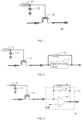
- FIG.1 is a schematic view of a switch control circuit 10 provided by an embodiment of the present disclosure; the switch control circuit 10 comprises: a first control switch 21, a first capacitor 22 and a field-effect transistor switch 23.
- the first control switch 21 is connected to a signal source, wherein the signal source is configured to output the power source signal VDD to the subsequent circuit when the first control switch 21 is turned on.
- the first control switch 21 is configured to receive the power source signal, and control the ON-OFF state of the power source signal; the first end of first capacitor 22 is connected to the first end of the first control switch 21, the second end of the first capacitor 22 is grounded, the first capacitor 22 is configured to receive the power source signal VDD for charging, when the first control switch 21 is turned on, and the first capacitor 22 is also configured to release electrical energy when the first control switch 21 is turned off, the gate electrode of the field-effect transistor switch 23 is connected to the first end of the first capacitor 22, optionally, the charging voltage released when the first capacitor 22 is discharged is greater than the ON voltage drop of the field-effect transistor switch 23, and when the first capacitor 22 is discharged, the field-effect transistor switch 23 controls the field-effect transistor switch 23 to be turned on by the charging voltage released by the first capacitor 22.
- the field-effect transistor switch 23 and the first control switch 21 may be N-Metal-Oxide-Semiconductor (NMOS) switches, Positive channel Metal Oxide Semiconductor (PMOS) switches or Complementary Metal Oxide Semiconductor (CMOS) switches.
- NMOS N-Metal-Oxide-Semiconductor
- PMOS Positive channel Metal Oxide Semiconductor
- CMOS Complementary Metal Oxide Semiconductor
- the first capacitor 22 when the first control switch 21 is turned off, the first capacitor 22 is converted from a charged state to a discharged state, and the charging voltage released by the first capacitor 22 can control the field-effect transistor switch 23 to be turned on, at this time, since the first control switch 21 is turned off, the power source signal VDD cannot reach the gate electrode of the field-effect transistor switch 23, so the power source noise cannot be coupled into the circuit where the source and drain electrodes of the field-effect transistor switch 23 are located, therefore, when the first capacitor 22 is in discharging phase, the discharge voltage of the first capacitor 22 can be used as a control signal of the field-effect transistor switch 23 to control the field-effect transistor switch 23 to be turned on, thereby reducing the power source coupling noise.
- the switch control circuit further comprises a second control switch 26 and a signal processing circuit 27.
- the second control switch 26 is connected to the drain electrode of the field-effect transistor switch 23, and controls the second control switch 26 to be turned on when the first capacitor 22 is charged, and to be turned off when first capacitor 22 is discharged. That is, when the first control switch 21 is turned on, the second control switch 26 is turned on; and when the first control switch 21 is turned off, the second control switch 26 is turned off.
- the signal processing circuit 27 is connected in parallel with the second control switch 26, wherein the signal processing circuit 27 is configured to process the input analog signal when the second control switch 26 is turned off.
- the second control switch 26 when the first control switch 21 is turned on, the first capacitor 22 is charged, and the field-effect transistor switch 23 is turned on, at this time, in order to prevent power source noise from being coupled into the analog signal received by the signal processing circuit 27, the second control switch 26 is turned on, so that the analog signal is directly output through the second control switch 26 without passing through the signal processing circuit 27.
- the first control switch 21 When the first control switch 21 is turned off, the first capacitor 22 is discharged and the field-effect transistor switch 23 is turned on, at this time, the power source noise may not be coupled into field-effect transistor switch 23, and the second control switch 26 is controlled to be turned off, the analog signal may be processed by the signal processing circuit 27, thereby reducing the noise contained in the analog signal.
- the signal processing circuit 27 is an analog front end (Analog Front End, AFE).
- the analog front end comprises: an operational amplifier 24 and a sampling capacitor 25.
- the reverse input end of the operational amplifier 24 is connected to the drain electrode of the field-effect transistor switch 23, and the forward input end of the operational amplifier 24 is configured to receive the reference voltage; one end of the sampling capacitor 25 is connected to the reverse input end of the operational amplifier 24, and the other end of the sampling capacitor 25 is connected to the output end of the operational amplifier 24; and the second control switch 26 is connected in parallel to two ends of the sampling capacitor 25.
- FIG. 4 shows a timing schematic view of the ON and OFF of each switch, and as it may be affected by different factors in actual situations, the ON or OFF of the first control switch 21 and the second control switch 26 may not be completely synchronized, and the slight time difference may be ignored.
- the signal processing circuit 27 works in an amplified state.
- the signal processing circuit 27 works in a reset state.
- FIG. 5 is a state view that matches the ON/OFF conditions and the analog front end states of switches in the circuit shown in the timing view of FIG. 4 .
- the first control switch 21 is ON
- the second control switch 26 is ON or OFF.
- gate electrode input signal of the first control switch 21 is at a low level, the source and drain electrodes of the first control switch 21 are turned off (non-conduction), and gate electrode input signal of the field-effect transistor switch 23 is at a low level, the source electrode and drain electrode of the field-effect transistor switch 23 are turned off (non-conduction), so the signal is not transmitted to the signal processing circuit 27.
- the signal processing circuit 27 is in a reset (RST) or amplified (AMP) state.
- the first control switch 21 receives the power source signal VDD (high level), and the first control switch 21 and the second control switch 26 are both ON.
- the first control switch 21 receives the power source signal VDD
- the first capacitor is charged
- the gate electrode input signal of the field-effect transistor switch 23 is at a high level
- the source electrode and drain electrode of the field-effect transistor switch 23 are turned on (conduction). Since the second control switch 26 is ON during this time period, the input signal is directly output through the second control switch 26, and may not enter the signal processing circuit 27 for processing.
- the signal processing circuit 27 is in a reset state.
- FIG. 8 is structural schematic view of a multiplexer switch circuit 20 provided by the present embodiment.
- the multiplexer switch circuit 20 comprises a switch array 31, wherein the switch array 31 comprises multiple groups of the switch control circuits 10, and the multiple groups of the switch control circuits 10 are connected in parallel.
- the switch array 31 comprising 5 groups of switch control circuits 10 is taken as an example, and this application is not limited to this.
- the structure of each group of switch control circuits 10 can be as shown in FIG. 1 , and may not be repeated here.
- the power source signals of the first group of switch control circuits 10 may be controlled to be at a high level, and the power source signals of other groups of switch control circuits are at a low level, so that only the first capacitor 22 of the first group of switch control circuits 10 is charged, therefore, in the discharging phase of the first capacitor 22, only the field-effect transistor switch 23 of the first group of switch control circuits 10 may be turned on, and only one line may be selected for signal transmission.
- the multiplexer switch circuit 20 may further comprise: a second control switch 26 and a signal processing circuit 27, wherein the second control switch 26 is connected to the drain electrode of the field-effect transistor switch 23 in each group of switch control circuits 10, and configured to be turned on when the first capacitor 22 of the switch control circuit 10 is charged, and to be turned off when the first capacitor 22 is discharged.
- the signal processing circuit 27 is connected in parallel with the second control switch 26, wherein the signal processing circuit 27 is configured to process, in the case that the second control switch 26 is OFF, the analog signal transmitted by the field-effect transistor switch 23 in the switch control circuit 10.
- the signal processing circuit 27 comprises: an operational amplifier 24 and a sampling capacitor 25, wherein the reverse input end of the operational amplifier 24 is connected to the drain electrode of the field-effect transistor switch 23 in each group of switch control circuits 10, and the forward input end of the operational amplifier 24 is configured to input the reference voltage; and one end of the sampling capacitor 25 is connected to the reverse input end of the operational amplifier 24, and the other end of the sampling capacitor 25 is connected to the output end of the operational amplifier 24; wherein the second control switch 26 is connected in parallel to two ends of the sampling capacitor 25.
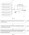
- FIG.11 is a flowchart schematic view of a control method provided by an embodiment of the present disclosure. This method may be applied to the multiplexer switch circuit described in the foregoing embodiments. The method may comprise the following steps.
- Step 810 transmitting a power source signal to the first control switch of at least one group of switch control circuits.
- the high level signal of the power source is transmitted to the first control switch of one group of switch control circuits, and the low level signal is transmitted to the first control switch of the other groups of switch control circuits.
- Step 811 controlling the first control switch to be turned on, and charging the first capacitor through the power source signal.
- the multiplexer switch circuit further comprises: at least one group of second control switch and signal processing circuit, wherein the second control switch is connected in parallel to the signal processing circuit, and the signal processing circuit is connected to each group of switch control circuits; therefore, in the case that the first control switch is ON the second control switch may also be controlled to be turned on, so that the analog signal transmitted by the field-effect transistor switch is output through the second control switch.
- Step 812 controlling the first control switch to be turned off, after the charging is completed, and using the charging voltage released by the first capacitor to drive the field-effect transistor switch to be turned on.
- the second control switch may be controlled to be turned off, when the first control switch is turned off, such that the analog signal transmitted by the field-effect transistor switch is processed through the signal processing circuit.
- the switch control circuit, the multiplexer switch circuit and the control method for a multiplexer switch control circuit provided by the embodiments of the present disclosure, when the first control switch is turned off, the charging voltage released by the first capacitor can control the field-effect transistor switch to be turned on, at this time, because the first control switch is turned off, the power source signal cannot reach the gate electrode of the field-effect transistor switch, so the power source noise cannot be coupled into the circuit where the source and drain electrodes of the field-effect transistor switch are located, therefore, in the discharge stage of first capacitor, the discharge voltage can be used as a control signal to control the field-effect transistor switch to be turned on, thereby reducing power source coupling noise.
Landscapes
- Engineering & Computer Science (AREA)
- Power Engineering (AREA)
- Physics & Mathematics (AREA)
- Electromagnetism (AREA)
- Electronic Switches (AREA)
Claims (12)
- Schaltsteuerungskreis (10), umfassend:einen ersten Steuerungsschalter (21), der dazu konfiguriert ist, beim Einschalten ein Stromquellensignal zu übertragen;einen ersten Kondensator (22), wobei der erste Kondensator (22) mit dem ersten Steuerungsschalter (21) verbunden ist und dazu konfiguriert ist, das Stromquellensignal zum Laden zu empfangen und eine Ladespannung freizugeben, wenn der erste Steuerungsschalter (21) ausgeschaltet ist; undeinen Feldeffekttransistorschalter (23), der mit dem ersten Kondensator (22) verbunden ist,wobei der Feldeffekttransistorschalter (23) dazu konfiguriert ist, die durch den ersten Kondensator (22) freigegebene Ladespannung zu empfangen, um ein Einschalten des Feldeffekttransistorschalters (23) zu steuern;einen zweiten Steuerungsschalter (26), der mit einer Drain-Elektrode des Feldeffekttransistorschalters (23) verbunden ist und dazu konfiguriert ist, eingeschaltet zu werden, wenn der erste Kondensator (22) geladen wird, und ausgeschaltet zu werden, wenn der erste Kondensator (22) entladen wird; undeinen Signalverarbeitungskreis (27), der parallel zu zwei Enden des zweiten Steuerungsschalters (26) verbunden ist, wobei der Signalverarbeitungskreis (27) dazu konfiguriert ist, ein durch den Feldeffekttransistorschalter (23) übertragenes analoges Signal zu verarbeiten, wenn der zweite Steuerungsschalter (26) ausgeschaltet ist;wobei der Signalverarbeitungskreis (27) ein analoges Frontend ist und das analoge Frontend Folgendes umfasst:einen Operationsverstärker (24), wobei ein Rückwärtseingangsende des Operationsverstärkers (24) mit der Drain-Elektrode des Feldeffekttransistorschalters (23) verbunden ist und ein Vorwärtseingangsende des Operationsverstärkers (24) dazu konfiguriert ist, eine Referenzspannung zu empfangen; undeinen Abtastkondensator (25), wobei ein Ende des Abtastkondensators (25) mit dem Rückwärtseingangsende des Operationsverstärkers (24) verbunden ist und das andere Ende mit einem Ausgangsende des Operationsverstärkers (24) verbunden ist,wobei der zweite Steuerungsschalter (26) parallel zu zwei Enden des Abtastkondensators (25) verbunden ist,wobei ein Arbeitszustand des Signalverarbeitungskreises (27) einen zurückgesetzten Zustand und einen verstärkten Zustand umfasst;wobei der Signalverarbeitungskreis (27) im zurückgesetzten Zustand betrieben wird, wenn der erste Steuerungsschalter (21) eingeschaltet ist und der zweite Steuerungsschalter (26) eingeschaltet ist; undwobei der Signalverarbeitungskreis (27) im verstärkten Zustand betrieben wird, wenn der erste Steuerungsschalter (21) ausgeschaltet ist und der zweite Steuerungsschalter (26) ausgeschaltet ist.
- Schaltsteuerungskreis (10) nach Anspruch 1, wobei ein erstes Ende des ersten Steuerungsschalters (21) dazu konfiguriert ist, das Stromquellensignal zu empfangen, und ein zweites Ende des ersten Steuerungsschalters (21) elektrisch mit einem ersten Ende des ersten Kondensators (22) verbunden ist;ein zweites Ende des ersten Kondensators (22) geerdet ist; undeine Gate-Elektrode des Feldeffekttransistorschalters (23) mit dem ersten Ende des ersten Kondensators (22) verbunden ist.
- Schaltsteuerungskreis (10) nach Anspruch 1, wobei die durch den ersten Kondensator (22) freigegebene Ladespannung größer ist als ein EIN-Spannungsabfall des Feldeffekttransistorschalters (23).
- Schaltsteuerungskreis (10) nach einem der Ansprüche 1-3, wobei der Feldeffekttransistorschalter (23) einen NMOS-Schalter, einen PMOS-Schalter oder einen CMOS-Schalter umfasst.
- Multiplexerschaltkreis, umfassend:ein Schalterarray, das mehrere Gruppen von Schaltsteuerungskreisen (10) umfasst,wobei jede Gruppe von Schaltsteuerungskreisen (10) den Schaltsteuerungskreis (10) nach einem der Ansprüche 1-4 umfasst.
- Multiplexerschaltkreis nach Anspruch 5, ferner umfassend:mindestens eine Gruppe aus einem zweiten Steuerungsschalter (26) und einem Signalverarbeitungskreis (27), wobei der zweite Steuerungsschalter (26) mit einer Drain-Elektrode des Feldeffekttransistorschalters (23) in jeder Gruppe von Schaltsteuerungskreisen (10) verbunden ist und dazu konfiguriert ist, eingeschaltet zu werden, wenn der erste Kondensator (22) geladen wird, und ausgeschaltet zu werden, wenn der erste Kondensator (22) entladen wird; undder Signalverarbeitungskreis (27) parallel zu zwei Enden des zweiten Steuerungsschalters (26) verbunden ist und der Signalverarbeitungskreis (27) dazu konfiguriert ist, ein durch den Feldeffekttransistorschalter (23) übertragenes analoges Signal zu verarbeiten, wenn der zweite Steuerungsschalter (26) ausgeschaltet ist.
- Multiplexerschaltkreis nach Anspruch 6, wobei der Signalverarbeitungskreis (27) ein analoges Frontend ist und das analoge Frontend Folgendes umfasst:einen Operationsverstärker (24), wobei ein Rückwärtseingangsende des Operationsverstärkers (24) mit der Drain-Elektrode des Feldeffekttransistorschalters (23) in jeder Gruppe von Schaltsteuerungskreisen (10) verbunden ist und ein Vorwärtseingangsende dazu konfiguriert ist, eine Referenzspannung zu empfangen; undeinen Abtastkondensator (25), wobei ein Ende des Abtastkondensators (25) mit dem Rückwärtseingangsende des Operationsverstärkers (24) verbunden ist und das andere Ende mit einem Ausgangsende des Operationsverstärkers (24) verbunden ist.
- Multiplexerschaltkreis nach Anspruch 7, wobei der zweite Steuerungsschalter (26) parallel zu zwei Enden des Abtastkondensators (25) verbunden ist.
- Steuerungsverfahren, wobei das Verfahren auf den Multiplexerschaltkreis nach einem der Ansprüche 5-8 anwendbar ist und das Verfahren Folgendes umfasst:Übertragen eines Stromquellensignals an den ersten Steuerungsschalter (21) von mindestens einer Gruppe von Schaltsteuerungskreisen (10);Steuern eines Einschaltens des ersten Steuerungsschalters (21) und Laden des ersten Kondensators (22) über das Stromquellensignal; undSteuern eines Ausschaltens des ersten Steuerungsschalters (21), nachdem das Laden abgeschlossen ist, und Verwenden einer durch den ersten Kondensator (22) freigegebenen Ladespannung, um den Feldeffekttransistorschalter (23) so anzutreiben, dass er eingeschaltet wird.
- Steuerungsverfahren nach Anspruch 9, wobei das Stromquellensignal ein Hochpegelsignal ist und das Verfahren ferner Folgendes umfasst:
Steuern und Eingeben eines Niederpegelsignals an den/die ersten Steuerungsschalter, an dem/denen kein Stromquellensignal eingegeben wird. - Steuerungsverfahren nach Anspruch 9, wobei der Multiplexerschaltkreis ferner Folgendes umfasst: mindestens eine Gruppe aus einem zweiten Steuerungsschalter (26) und einem Signalverarbeitungskreis (27), wobei der zweite Steuerungsschalter (26) parallel zu dem Signalverarbeitungskreis (27) verbunden ist und der Signalverarbeitungskreis (27) mit jeder Gruppe von Schaltsteuerungskreisen (10) verbunden ist; und das Verfahren ferner Folgendes umfasst:
Steuern eines Ausschaltens des zweiten Steuerungsschalters (26), wenn der erste Steuerungsschalter (21) ausgeschaltet ist, wobei ein durch den Feldeffekttransistorschalter (23) übertragenes analoges Signal über den Signalverarbeitungskreis (27) verarbeitet wird. - Verfahren nach Anspruch 11, ferner umfassend:
Steuern eines Einschaltens des zweiten Steuerungsschalters (26), wenn der erste Steuerungsschalter (21) eingeschaltet ist, wobei das durch den Feldeffekttransistorschalter (23) übertragene analoge Signal über den zweiten Steuerungsschalter (26) ausgegeben wird.
Applications Claiming Priority (2)
| Application Number | Priority Date | Filing Date | Title |
|---|---|---|---|
| CN202010039535.5A CN111245218B (zh) | 2020-01-14 | 2020-01-14 | 开关控制电路、多路选择开关电路及其控制方法 |
| PCT/CN2020/137334 WO2021143450A1 (zh) | 2020-01-14 | 2020-12-17 | 开关控制电路、多路选择开关电路以及多路选择开关控制电路的控制方法 |
Publications (4)
| Publication Number | Publication Date |
|---|---|
| EP3975405A1 EP3975405A1 (de) | 2022-03-30 |
| EP3975405A4 EP3975405A4 (de) | 2022-09-07 |
| EP3975405B1 true EP3975405B1 (de) | 2025-02-12 |
| EP3975405C0 EP3975405C0 (de) | 2025-02-12 |
Family
ID=70879477
Family Applications (1)
| Application Number | Title | Priority Date | Filing Date |
|---|---|---|---|
| EP20913988.0A Active EP3975405B1 (de) | 2020-01-14 | 2020-12-17 | Schaltsteuerungskreis, multiplexerschaltkreis und steuerungsverfahren für multiplexerschaltsteuerungskreis |
Country Status (5)
| Country | Link |
|---|---|
| US (1) | US20230006608A1 (de) |
| EP (1) | EP3975405B1 (de) |
| KR (1) | KR102675668B1 (de) |
| CN (1) | CN111245218B (de) |
| WO (1) | WO2021143450A1 (de) |
Families Citing this family (2)
| Publication number | Priority date | Publication date | Assignee | Title |
|---|---|---|---|---|
| CN111245218B (zh) * | 2020-01-14 | 2021-09-17 | 北京集创北方科技股份有限公司 | 开关控制电路、多路选择开关电路及其控制方法 |
| CN116225197B (zh) * | 2023-05-08 | 2023-08-29 | 核芯互联科技(青岛)有限公司 | 电压模式驱动方法及电路 |
Family Cites Families (11)
| Publication number | Priority date | Publication date | Assignee | Title |
|---|---|---|---|---|
| US5856812A (en) * | 1993-05-11 | 1999-01-05 | Micron Display Technology, Inc. | Controlling pixel brightness in a field emission display using circuits for sampling and discharging |
| FR2832537B1 (fr) * | 2001-11-16 | 2003-12-19 | Commissariat Energie Atomique | Procede et dispositif de commande en tension d'une source d'electrons a structure matricielle, avec regulation de la charge emise |
| CN101587753B (zh) * | 2009-06-26 | 2014-12-31 | 北京中星微电子有限公司 | 一种模拟信号采样电路以及一种开关电容电路 |
| CN202435332U (zh) * | 2011-12-23 | 2012-09-12 | 东南大学 | 低成本、高隔离特性的开关磁阻电机自举式驱动电路 |
| US8847631B2 (en) * | 2011-12-23 | 2014-09-30 | General Electric Company | High speed low loss gate drive circuit |
| US9811205B2 (en) * | 2015-09-29 | 2017-11-07 | Synaptics Incorporated | Variable time anti-aliasing filter |
| JP7011544B2 (ja) * | 2018-06-28 | 2022-02-10 | 株式会社日立インダストリアルプロダクツ | 電力変換装置 |
| CN109461730B (zh) * | 2018-12-20 | 2024-05-17 | 北京集创北方科技股份有限公司 | 静电防护电路及静电防护装置 |
| CN110196653B (zh) * | 2019-04-26 | 2020-09-11 | 北京集创北方科技股份有限公司 | 触摸检测电路、触控显示装置以及触摸检测方法 |
| CN209913796U (zh) * | 2019-04-29 | 2020-01-07 | 深圳市嗨兴科技有限公司 | 一种开关电路 |
| CN111245218B (zh) * | 2020-01-14 | 2021-09-17 | 北京集创北方科技股份有限公司 | 开关控制电路、多路选择开关电路及其控制方法 |
-
2020
- 2020-01-14 CN CN202010039535.5A patent/CN111245218B/zh active Active
- 2020-12-17 WO PCT/CN2020/137334 patent/WO2021143450A1/zh not_active Ceased
- 2020-12-17 EP EP20913988.0A patent/EP3975405B1/de active Active
- 2020-12-17 US US17/781,181 patent/US20230006608A1/en active Pending
- 2020-12-17 KR KR1020227005542A patent/KR102675668B1/ko active Active
Also Published As
| Publication number | Publication date |
|---|---|
| US20230006608A1 (en) | 2023-01-05 |
| CN111245218A (zh) | 2020-06-05 |
| EP3975405A4 (de) | 2022-09-07 |
| WO2021143450A1 (zh) | 2021-07-22 |
| EP3975405C0 (de) | 2025-02-12 |
| KR20220035478A (ko) | 2022-03-22 |
| EP3975405A1 (de) | 2022-03-30 |
| CN111245218B (zh) | 2021-09-17 |
| KR102675668B1 (ko) | 2024-06-14 |
Similar Documents
| Publication | Publication Date | Title |
|---|---|---|
| US6897696B2 (en) | Duty-cycle adjustable buffer and method and method for operating same | |
| US5554892A (en) | Signal processing circuit for switch capable of reducing insertion loss | |
| US5945867A (en) | Switch circuit device | |
| EP3975405B1 (de) | Schaltsteuerungskreis, multiplexerschaltkreis und steuerungsverfahren für multiplexerschaltsteuerungskreis | |
| US7924055B2 (en) | Data transmitting system | |
| US20170249913A1 (en) | Display driving device | |
| DE10344878A1 (de) | Differenzverstärkeranordnung mit Stromregelkreis und Verfahren zum Betreiben einer Differenzverstärkeranordnung | |
| CN107168452B (zh) | 一种按键输入处理电路 | |
| US10608653B2 (en) | Digital-to-analog conversion circuit | |
| US6429692B1 (en) | High speed data sampling with reduced metastability | |
| US20070157004A1 (en) | Multi purpose switching circuit and electronic apparatus including same | |
| JPH0763138B2 (ja) | 論理デ−タ伝送バスの予負荷回路 | |
| EP3573243A1 (de) | Eingabevorrichtung, steuerungsverfahren der eingabevorrichtung | |
| EP2536010A2 (de) | Stromerzeugungsschaltung und Schaltkreis | |
| EP0393996B1 (de) | Ladungsgekoppelte Vorrichtungen | |
| US6378026B1 (en) | Connection detection circuit and method | |
| JP3384045B2 (ja) | シンクチップクランプ/同期分離回路 | |
| US3063016A (en) | Binary counting circuits | |
| US5477173A (en) | Ultra low power gain circuit (UGC) | |
| US5751167A (en) | CMOS output buffer circuit which converts CMOS logic signals to ECL logic signals and which discharges parasitic load capacitances | |
| US20160149391A1 (en) | Over-voltage protection circuit | |
| WO2001047103A2 (en) | Electronic circuit | |
| KR20010060330A (ko) | 신호전송회로 | |
| US20070046358A1 (en) | Quick turn on apparatus and method for a NMOSFET switch | |
| EP0272688A2 (de) | Ausgangsverstärker für eine Ladungsübertragungseinrichtung |
Legal Events
| Date | Code | Title | Description |
|---|---|---|---|
| STAA | Information on the status of an ep patent application or granted ep patent |
Free format text: STATUS: THE INTERNATIONAL PUBLICATION HAS BEEN MADE |
|
| PUAI | Public reference made under article 153(3) epc to a published international application that has entered the european phase |
Free format text: ORIGINAL CODE: 0009012 |
|
| STAA | Information on the status of an ep patent application or granted ep patent |
Free format text: STATUS: REQUEST FOR EXAMINATION WAS MADE |
|
| 17P | Request for examination filed |
Effective date: 20211223 |
|
| AK | Designated contracting states |
Kind code of ref document: A1 Designated state(s): AL AT BE BG CH CY CZ DE DK EE ES FI FR GB GR HR HU IE IS IT LI LT LU LV MC MK MT NL NO PL PT RO RS SE SI SK SM TR |
|
| STAA | Information on the status of an ep patent application or granted ep patent |
Free format text: STATUS: EXAMINATION IS IN PROGRESS |
|
| A4 | Supplementary search report drawn up and despatched |
Effective date: 20220810 |
|
| RIC1 | Information provided on ipc code assigned before grant |
Ipc: H02M 1/44 20070101ALI20220804BHEP Ipc: H02M 3/07 20060101AFI20220804BHEP |
|
| 17Q | First examination report despatched |
Effective date: 20220823 |
|
| DAV | Request for validation of the european patent (deleted) | ||
| DAX | Request for extension of the european patent (deleted) | ||
| GRAP | Despatch of communication of intention to grant a patent |
Free format text: ORIGINAL CODE: EPIDOSNIGR1 |
|
| STAA | Information on the status of an ep patent application or granted ep patent |
Free format text: STATUS: GRANT OF PATENT IS INTENDED |
|
| INTG | Intention to grant announced |
Effective date: 20240909 |
|
| GRAS | Grant fee paid |
Free format text: ORIGINAL CODE: EPIDOSNIGR3 |
|
| GRAA | (expected) grant |
Free format text: ORIGINAL CODE: 0009210 |
|
| STAA | Information on the status of an ep patent application or granted ep patent |
Free format text: STATUS: THE PATENT HAS BEEN GRANTED |
|
| AK | Designated contracting states |
Kind code of ref document: B1 Designated state(s): AL AT BE BG CH CY CZ DE DK EE ES FI FR GB GR HR HU IE IS IT LI LT LU LV MC MK MT NL NO PL PT RO RS SE SI SK SM TR |
|
| REG | Reference to a national code |
Ref country code: GB Ref legal event code: FG4D |
|
| REG | Reference to a national code |
Ref country code: CH Ref legal event code: EP |
|
| REG | Reference to a national code |
Ref country code: DE Ref legal event code: R096 Ref document number: 602020046144 Country of ref document: DE |
|
| REG | Reference to a national code |
Ref country code: IE Ref legal event code: FG4D |
|
| U01 | Request for unitary effect filed |
Effective date: 20250307 |
|
| U07 | Unitary effect registered |
Designated state(s): AT BE BG DE DK EE FI FR IT LT LU LV MT NL PT RO SE SI Effective date: 20250314 |
|
| PG25 | Lapsed in a contracting state [announced via postgrant information from national office to epo] |
Ref country code: RS Free format text: LAPSE BECAUSE OF FAILURE TO SUBMIT A TRANSLATION OF THE DESCRIPTION OR TO PAY THE FEE WITHIN THE PRESCRIBED TIME-LIMIT Effective date: 20250512 |
|
| PG25 | Lapsed in a contracting state [announced via postgrant information from national office to epo] |
Ref country code: PL Free format text: LAPSE BECAUSE OF FAILURE TO SUBMIT A TRANSLATION OF THE DESCRIPTION OR TO PAY THE FEE WITHIN THE PRESCRIBED TIME-LIMIT Effective date: 20250212 |
|
| PG25 | Lapsed in a contracting state [announced via postgrant information from national office to epo] |
Ref country code: ES Free format text: LAPSE BECAUSE OF FAILURE TO SUBMIT A TRANSLATION OF THE DESCRIPTION OR TO PAY THE FEE WITHIN THE PRESCRIBED TIME-LIMIT Effective date: 20250212 |
|
| PG25 | Lapsed in a contracting state [announced via postgrant information from national office to epo] |
Ref country code: NO Free format text: LAPSE BECAUSE OF FAILURE TO SUBMIT A TRANSLATION OF THE DESCRIPTION OR TO PAY THE FEE WITHIN THE PRESCRIBED TIME-LIMIT Effective date: 20250512 Ref country code: IS Free format text: LAPSE BECAUSE OF FAILURE TO SUBMIT A TRANSLATION OF THE DESCRIPTION OR TO PAY THE FEE WITHIN THE PRESCRIBED TIME-LIMIT Effective date: 20250612 |
|
| PG25 | Lapsed in a contracting state [announced via postgrant information from national office to epo] |
Ref country code: HR Free format text: LAPSE BECAUSE OF FAILURE TO SUBMIT A TRANSLATION OF THE DESCRIPTION OR TO PAY THE FEE WITHIN THE PRESCRIBED TIME-LIMIT Effective date: 20250212 |
|
| PG25 | Lapsed in a contracting state [announced via postgrant information from national office to epo] |
Ref country code: GR Free format text: LAPSE BECAUSE OF FAILURE TO SUBMIT A TRANSLATION OF THE DESCRIPTION OR TO PAY THE FEE WITHIN THE PRESCRIBED TIME-LIMIT Effective date: 20250513 |
|
| PG25 | Lapsed in a contracting state [announced via postgrant information from national office to epo] |
Ref country code: SM Free format text: LAPSE BECAUSE OF FAILURE TO SUBMIT A TRANSLATION OF THE DESCRIPTION OR TO PAY THE FEE WITHIN THE PRESCRIBED TIME-LIMIT Effective date: 20250212 |
|
| PG25 | Lapsed in a contracting state [announced via postgrant information from national office to epo] |
Ref country code: CZ Free format text: LAPSE BECAUSE OF FAILURE TO SUBMIT A TRANSLATION OF THE DESCRIPTION OR TO PAY THE FEE WITHIN THE PRESCRIBED TIME-LIMIT Effective date: 20250212 |
|
| PG25 | Lapsed in a contracting state [announced via postgrant information from national office to epo] |
Ref country code: SK Free format text: LAPSE BECAUSE OF FAILURE TO SUBMIT A TRANSLATION OF THE DESCRIPTION OR TO PAY THE FEE WITHIN THE PRESCRIBED TIME-LIMIT Effective date: 20250212 |
|
| PLBE | No opposition filed within time limit |
Free format text: ORIGINAL CODE: 0009261 |
|
| STAA | Information on the status of an ep patent application or granted ep patent |
Free format text: STATUS: NO OPPOSITION FILED WITHIN TIME LIMIT |
|
| U20 | Renewal fee for the european patent with unitary effect paid |
Year of fee payment: 6 Effective date: 20251127 |
|
| 26N | No opposition filed |
Effective date: 20251113 |