EP3573243A1 - Eingabevorrichtung, steuerungsverfahren der eingabevorrichtung - Google Patents
Eingabevorrichtung, steuerungsverfahren der eingabevorrichtung Download PDFInfo
- Publication number
- EP3573243A1 EP3573243A1 EP19175495.1A EP19175495A EP3573243A1 EP 3573243 A1 EP3573243 A1 EP 3573243A1 EP 19175495 A EP19175495 A EP 19175495A EP 3573243 A1 EP3573243 A1 EP 3573243A1
- Authority
- EP
- European Patent Office
- Prior art keywords
- input
- switches
- output
- switch
- control part
- Prior art date
- Legal status (The legal status is an assumption and is not a legal conclusion. Google has not performed a legal analysis and makes no representation as to the accuracy of the status listed.)
- Withdrawn
Links
Images


Classifications
-
- H—ELECTRICITY
- H03—ELECTRONIC CIRCUITRY
- H03M—CODING; DECODING; CODE CONVERSION IN GENERAL
- H03M11/00—Coding in connection with keyboards or like devices, i.e. coding of the position of operated keys
-
- H—ELECTRICITY
- H03—ELECTRONIC CIRCUITRY
- H03K—PULSE TECHNIQUE
- H03K17/00—Electronic switching or gating, i.e. not by contact-making and –breaking
- H03K17/94—Electronic switching or gating, i.e. not by contact-making and –breaking characterised by the way in which the control signals are generated
- H03K17/96—Touch switches
- H03K17/9645—Resistive touch switches
-
- G—PHYSICS
- G06—COMPUTING OR CALCULATING; COUNTING
- G06F—ELECTRIC DIGITAL DATA PROCESSING
- G06F3/00—Input arrangements for transferring data to be processed into a form capable of being handled by the computer; Output arrangements for transferring data from processing unit to output unit, e.g. interface arrangements
- G06F3/01—Input arrangements or combined input and output arrangements for interaction between user and computer
- G06F3/02—Input arrangements using manually operated switches, e.g. using keyboards or dials
-
- H—ELECTRICITY
- H01—ELECTRIC ELEMENTS
- H01H—ELECTRIC SWITCHES; RELAYS; SELECTORS; EMERGENCY PROTECTIVE DEVICES
- H01H9/00—Details of switching devices, not covered by groups H01H1/00 - H01H7/00
- H01H9/54—Circuit arrangements not adapted to a particular application of the switching device and for which no provision exists elsewhere
-
- H—ELECTRICITY
- H03—ELECTRONIC CIRCUITRY
- H03K—PULSE TECHNIQUE
- H03K17/00—Electronic switching or gating, i.e. not by contact-making and –breaking
- H03K17/18—Modifications for indicating state of switch
-
- H—ELECTRICITY
- H03—ELECTRONIC CIRCUITRY
- H03K—PULSE TECHNIQUE
- H03K17/00—Electronic switching or gating, i.e. not by contact-making and –breaking
- H03K17/51—Electronic switching or gating, i.e. not by contact-making and –breaking characterised by the components used
- H03K17/56—Electronic switching or gating, i.e. not by contact-making and –breaking characterised by the components used by the use, as active elements, of semiconductor devices
- H03K17/687—Electronic switching or gating, i.e. not by contact-making and –breaking characterised by the components used by the use, as active elements, of semiconductor devices the devices being field-effect transistors
Definitions
- the present invention relates to an improved technique of an input device used for an operator to input an instruction to various electronic devices, etc.
- a prior art of an input device used for an operator to input an instruction to various electronic devices, etc. is disclosed, in Japanese Unexamined Patent Application Publication No. 03-135298 , for example.
- the remote control disclosed in this document is provided with membrane switches arranged in a matrix, and an instruction can be input by pressing one of the membrane switches.
- FIG. 4 an example of a circuit configuration of the prior art input device provided with a plurality of switches as described above is shown.
- the input device shown in FIG. 4 is configured to include a control part 10a (abbreviated as CTRL PART in FIG. 4 ) comprising a microcomputer or the like, a plurality of switches 11 to 22 arranged in a matrix, resistance elements 31 to 38, and an element 40 for protection from reverse connection.
- the control part 10a includes a plurality of output terminals C11, C12, and C13, and a plurality of input terminals S1, S2, S3, and S4.
- Each of the output terminals C11 to C13 is connected to one end of one of the switches 11 to 22, and each of the input terminals S1 to S4 is connected to the other end of one of the switches 11 to 22.
- FIG. 5 a timing chart of the prior art input device shown in FIG. 4 during its operation is illustrated.
- the input device sets each of the output terminals C11 to C13 (abbreviated as C11 TERM, C12 TERM, C13 TERM, respectively, in FIG. 5 ) to low potentials (Lo OUTPUT) at different timings, and correspondingly, the voltage is detected at each of the input terminals S1 to S4 to determine that each of the switches 11 to 22 is pressed. For example, when the switch 11 is pressed, at the timing when the potential of the C11 terminal becomes low as shown in FIG.
- the control part 10a is able to determine that the switch 11 has been pressed. Further, even when the switches 11 and 12 are simultaneously pressed, since the timing at which each of the potentials of the output terminals C11 and C12 becomes low is different, the control part 10a is able to determine that each of the switches 11 and 12 is pressed.
- connection includes both (i) a case where specific circuit elements are directly connected to each other via a wiring or the like, and (ii) a case where another circuit element intervenes between the specific circuit elements, and the specific circuit elements are indirectly connected to each other.
- FIG. 1 is a diagram showing a circuit configuration of an input device according to one embodiment.
- the illustrated input device is configured to include a control part 10 (abbreviated as CTRL PART in FIG. 1 ) comprising a microcomputer or the like, a plurality of switches 11 to 22 arranged in a 4 ⁇ 3 matrix, and resistance elements 31 to 38.
- This input device detects whether or not each of the switches 11 to 22 has been pressed (that is, the detection of conductive state), and provides the detection result to a host device which is not shown in the figure.
- the host device described here may be various electronic devices such as an air conditioner, for example.
- the input device and the host device may be connected by wire or may be wirelessly connected.
- the control part 10 has a plurality of input/output terminals C1, C2 and C3 and a plurality of input terminals S1, S2, S3 and S4.
- Each of the input/output terminals C1 to C3 is a terminal capable of selecting either an "output state” which is a state that outputs a low potential signal (scan signal) having a relatively low potential, or an "input state (input reception state)" which is a state that inputs (detects) an externally applied signal to the control part 10.
- the switching of each state can be realized by executing a predetermined program in the control part 10.
- Each of the input terminals S1 to S4 is a terminal for inputting (detecting) an externally applied signal to the control part 10.
- the input terminal S1 of the control part 10 is connected to one end of each of the switches 11, 12, and 13 via a wire and the resistance element 35.
- the input terminal S2 is connected to one end of each of the switches 14, 15, and 16 via a wire and the resistance element 36.
- the input terminal S3 is connected to one end of each of the switches 17, 19, and 19 via a wire and the resistance element 37.
- the input terminal S4 is connected to one end of each of the switches 20, 21, and 22 via a wire and the resistance element 38.
- the input/output terminal C1 of the control part 10 is connected to the other end of each of the switches 11, 14, 17, and 20 via a wire.
- the input/output terminal C2 is connected to the other end of each of the switches 12, 15, 18, and 21 via a wire.
- the input/output terminal C3 is connected to the other end of each of the switches 13, 16, 19, and 22 via a wire.
- One end of the resistance element 31 is connected to a power supply terminal (high potential terminal), and the other end is connected between the input terminal S1 and one end of the switch 11.
- One end of the resistance element 32 is connected to the power supply terminal, and the other end is connected between the input terminal S2 and one end of the switch 14.
- One end of the resistance element 33 is connected to the power supply terminal, and the other end is connected between the input terminal S3 and one end of the switch 17.
- One end of the resistance element 34 is connected to the power supply terminal, and the other end is connected between the input terminal S4 and one end of the switch 20.
- the resistance element 35 is connected between the input terminal S1 and one end of the switch 11.
- the resistance element 36 is connected between the input terminal S2 and one end of the switch 14.
- the resistance element 37 is connected between the input terminal S3 and one end of the switch 17.
- the resistance element 38 is connected between the input terminal S4 and one end of the switch 20.
- FIG. 2 is a circuit diagram showing an example of the configuration of the internal circuit of the input/output terminal in the control part of the input device.
- the illustrated input/output circuit 50 is a circuit for switching the input/output terminal C1 to either the "output state" or the "input state", and is configured to include resistance elements 51 and 55, transistors 52, 53 and 54, a NAND element (NAND circuit) 56, a NOT element (NOT circuit) 57. Although the description is omitted here, the same input/output circuit 50 is provided for the other input/output terminals C2 and C3.
- resistance element 51 One end of the resistance element 51 is connected to the power supply terminal (high potential terminal), and the other end is connected to the transistor 52. Also, the resistance element 55 is connected between the input end of the NAND element 56 and the input/output terminal C1.
- the transistor 52 is a P-channel field effect transistor, for example, and one end of the current path (source/drain) is connected to the power supply terminal through the resistance element 51, and the other end of the current path (source/drain) is connected to the input/output terminal C1.
- a control signal Pull-up control
- the transistor 53 is a P-channel field effect transistor, for example, and one end of the current path (source/drain) is connected to the power supply terminal, and the other end of the current path (source/drain) is connected to the input/output terminal C1.
- a control signal (Pout) is provided to the control end (gate) of the transistor 53 from an internal circuit of the control part 10 which is not shown in the figure.
- the transistor 54 is a N-channel field effect transistor, for example, and one end of the current path (source/drain) is connected to the reference potential terminal (ground terminal), and the other end of the current path (source/drain) is connected to the input/output terminal C1.
- a control signal (Nout) is provided to the control end (gate) of the transistor 54 from an internal circuit of the control part 10 which is not shown in the figure.
- the first input end of the NAND element 56 is connected to the input/output terminal C1 via the resistance element 55, the second input end is connected to an internal circuit of the control part 10 which is not shown in the figure, and the output terminal is connected to the input end of NOT element 57.
- the second input end of the NAND element 56 receives a control signal (Standby control for input shutdown) from the internal circuit of the control part 10.
- the input end of the NOT element 57 is connected to the output end of the NAND element 56.
- the signal (Automotive input) obtained from the output end of the NOT element 57 corresponds to the externally applied signal via the input/output terminal C1.
- the circuit is arranged so that the externally applied signal (Analog input) can be directly obtained from the input/output terminal C1 via the resistance element 55.
- this input/output circuit 50 will be described below.
- the control part 10 sets the control signal (Standby control for input shutdown) to a predetermined potential and provides it to the second input end of the NAND element 56.
- the control part 10 acquires neither the signal obtained from the output end of the NOT element 57 (Automotive input) nor the signal (Analog input) obtained from the input/output terminal C1 via the resistance element 55.
- the control part 10 controls the potential of the control signals (Pout, Nout) applied to the control end of each of the transistors 53 and 54 so that the high potential signal or the low potential signal is not outputted, and then detects either the signal (Automotive input) obtained from the output end of the NOT element 57 or the signal (Analog input) obtained from the input/output terminal C1 via the resistance element 55.
- the input/output terminal C1 can be switched to the "output state” or the "input state”. At this time, the input/output terminal C1 is in a high impedance state in which a voltage can be detected without substantial current flow. The same applies to the other input/output terminals C2 and C3.
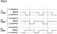
- FIG. 3 is a diagram showing a timing chart during the operation of the input device.
- the control part 10 of the input device sets each of the potentials of the input/output terminals C1 to C3 (abbreviated as C1 TERM., C2 TERM., C3 TERM. respectively, in FIG. 3 ) to a low potential at different timings, and detects voltages at each of the input terminals S1 to S4 correspondingly, thereby determines whether or not the switches 11 to 22 have been pressed.
- the control part 10 can detect that the switch 11 has become conductive and can determine that the switch has been pressed.
- the conductive state (conductive/non-conductive) of each switch is detected through the input terminals S2, S3, and S4. The same applies to the other input/output terminals C2 and C3, and the conductive state of each switch is detected at the timing when each of the input/output terminals C2 and C3 has a low potential.
- the control part 10 controls each of the input/output terminals C1 to C3 to the above-described "input state" in a period other than the period for outputting a low potential signal (the period of the above-described "output state”). That is, in the input device of the present embodiment, each input/output terminal C1 to C3 is controlled so that, while one input/output terminal (for example, the input/output terminal C1) is in the "output state", the other two input/output terminals (for example, the input/output terminals C2 and C3) are in the "input state".
Landscapes
- Engineering & Computer Science (AREA)
- Theoretical Computer Science (AREA)
- General Engineering & Computer Science (AREA)
- Human Computer Interaction (AREA)
- Physics & Mathematics (AREA)
- General Physics & Mathematics (AREA)
- Logic Circuits (AREA)
- Electronic Switches (AREA)
- Input From Keyboards Or The Like (AREA)
Applications Claiming Priority (1)
| Application Number | Priority Date | Filing Date | Title |
|---|---|---|---|
| JP2018099352A JP2019205072A (ja) | 2018-05-24 | 2018-05-24 | 入力装置、入力装置の制御方法 |
Publications (1)
| Publication Number | Publication Date |
|---|---|
| EP3573243A1 true EP3573243A1 (de) | 2019-11-27 |
Family
ID=66625792
Family Applications (1)
| Application Number | Title | Priority Date | Filing Date |
|---|---|---|---|
| EP19175495.1A Withdrawn EP3573243A1 (de) | 2018-05-24 | 2019-05-20 | Eingabevorrichtung, steuerungsverfahren der eingabevorrichtung |
Country Status (4)
| Country | Link |
|---|---|
| US (1) | US20190363713A1 (de) |
| EP (1) | EP3573243A1 (de) |
| JP (1) | JP2019205072A (de) |
| CN (1) | CN110531869A (de) |
Families Citing this family (2)
| Publication number | Priority date | Publication date | Assignee | Title |
|---|---|---|---|---|
| US12565401B2 (en) * | 2021-02-01 | 2026-03-03 | Otis Elevator Company | Elevator switch monitoring device |
| CN113948332B (zh) * | 2021-10-29 | 2024-03-22 | 广东美的厨房电器制造有限公司 | 按键的触发检测电路、按键组件和家电设备 |
Citations (3)
| Publication number | Priority date | Publication date | Assignee | Title |
|---|---|---|---|---|
| JPH03135298A (ja) | 1989-10-20 | 1991-06-10 | Matsushita Electric Ind Co Ltd | カード表示可変リモコン |
| US5430443A (en) * | 1993-04-12 | 1995-07-04 | National Semiconductor Corporation | Scanned switch matrix |
| JPH07202660A (ja) * | 1993-12-28 | 1995-08-04 | Aiphone Co Ltd | キーマトリックス回路 |
Family Cites Families (2)
| Publication number | Priority date | Publication date | Assignee | Title |
|---|---|---|---|---|
| US4906993A (en) * | 1988-04-04 | 1990-03-06 | John Fluke Mfg. Co., Inc. | Keyboard scanner apparatus and method |
| CN102075194B (zh) * | 2009-11-23 | 2015-03-11 | 鸿富锦精密工业(深圳)有限公司 | 键盘扫描电路和方法及电子设备 |
-
2018
- 2018-05-24 JP JP2018099352A patent/JP2019205072A/ja active Pending
-
2019
- 2019-05-20 US US16/416,277 patent/US20190363713A1/en not_active Abandoned
- 2019-05-20 EP EP19175495.1A patent/EP3573243A1/de not_active Withdrawn
- 2019-05-22 CN CN201910428119.1A patent/CN110531869A/zh active Pending
Patent Citations (3)
| Publication number | Priority date | Publication date | Assignee | Title |
|---|---|---|---|---|
| JPH03135298A (ja) | 1989-10-20 | 1991-06-10 | Matsushita Electric Ind Co Ltd | カード表示可変リモコン |
| US5430443A (en) * | 1993-04-12 | 1995-07-04 | National Semiconductor Corporation | Scanned switch matrix |
| JPH07202660A (ja) * | 1993-12-28 | 1995-08-04 | Aiphone Co Ltd | キーマトリックス回路 |
Also Published As
| Publication number | Publication date |
|---|---|
| US20190363713A1 (en) | 2019-11-28 |
| CN110531869A (zh) | 2019-12-03 |
| JP2019205072A (ja) | 2019-11-28 |
Similar Documents
| Publication | Publication Date | Title |
|---|---|---|
| US12062904B2 (en) | Current sense circuit | |
| US9825454B2 (en) | Protection device and method for electronic device | |
| EP3573243A1 (de) | Eingabevorrichtung, steuerungsverfahren der eingabevorrichtung | |
| JP5603674B2 (ja) | スイッチ装置および試験装置 | |
| US10756729B2 (en) | Electronic relay device | |
| US10564205B2 (en) | Voltage abnormality detection circuit and semiconductor device | |
| US11729566B2 (en) | Judging circuit for positive and negative terminals of mic of earphone and method thereof, and eletronic device | |
| US20060145731A1 (en) | Signal generating circuit | |
| US20160299546A1 (en) | Central processing unit protection circuit | |
| EP1678828B1 (de) | Schalter | |
| US6378026B1 (en) | Connection detection circuit and method | |
| US9153959B2 (en) | Phase detection circuit | |
| JP2012129936A (ja) | 駆動装置、スイッチ装置、および試験装置 | |
| US20200119729A1 (en) | Switch circuit and multiplexer applying the switch circuit | |
| US6014303A (en) | Overcurrent preventing device | |
| CN117081028A (zh) | 具有反接保护功能的直流电源传输电路 | |
| US10599202B2 (en) | Electronics device | |
| US8018326B2 (en) | Matrix switch | |
| US20040174217A1 (en) | Method and device for switch-on current limiting in push-pull amplifying power stages | |
| JP4808097B2 (ja) | 半導体スイッチ集積回路 | |
| US7902532B2 (en) | Systems and methods involving transducer signals | |
| KR100294211B1 (ko) | 집적회로간 버스 스톱 모드에 의한 시스템 조정 장치 | |
| US20200136499A1 (en) | Regulator device and control method thereof | |
| US7127533B2 (en) | Interrupt driven expanded option select interface for portable device | |
| US20160306702A1 (en) | Computer recovery circuit |
Legal Events
| Date | Code | Title | Description |
|---|---|---|---|
| PUAI | Public reference made under article 153(3) epc to a published international application that has entered the european phase |
Free format text: ORIGINAL CODE: 0009012 |
|
| AK | Designated contracting states |
Kind code of ref document: A1 Designated state(s): AL AT BE BG CH CY CZ DE DK EE ES FI FR GB GR HR HU IE IS IT LI LT LU LV MC MK MT NL NO PL PT RO RS SE SI SK SM TR |
|
| AX | Request for extension of the european patent |
Extension state: BA ME |
|
| STAA | Information on the status of an ep patent application or granted ep patent |
Free format text: STATUS: THE APPLICATION IS DEEMED TO BE WITHDRAWN |
|
| 18D | Application deemed to be withdrawn |
Effective date: 20200603 |