EP3975209A1 - Inductor framework structure, inductor device and lamp - Google Patents
Inductor framework structure, inductor device and lamp Download PDFInfo
- Publication number
- EP3975209A1 EP3975209A1 EP20862602.8A EP20862602A EP3975209A1 EP 3975209 A1 EP3975209 A1 EP 3975209A1 EP 20862602 A EP20862602 A EP 20862602A EP 3975209 A1 EP3975209 A1 EP 3975209A1
- Authority
- EP
- European Patent Office
- Prior art keywords
- end portion
- auxiliary
- winding part
- fixing
- main
- Prior art date
- Legal status (The legal status is an assumption and is not a legal conclusion. Google has not performed a legal analysis and makes no representation as to the accuracy of the status listed.)
- Granted
Links
Images




Classifications
-
- H—ELECTRICITY
- H01—ELECTRIC ELEMENTS
- H01F—MAGNETS; INDUCTANCES; TRANSFORMERS; SELECTION OF MATERIALS FOR THEIR MAGNETIC PROPERTIES
- H01F27/00—Details of transformers or inductances, in general
- H01F27/28—Coils; Windings; Conductive connections
- H01F27/288—Shielding
- H01F27/289—Shielding with auxiliary windings
-
- H—ELECTRICITY
- H01—ELECTRIC ELEMENTS
- H01F—MAGNETS; INDUCTANCES; TRANSFORMERS; SELECTION OF MATERIALS FOR THEIR MAGNETIC PROPERTIES
- H01F17/00—Fixed inductances of the signal type
- H01F17/04—Fixed inductances of the signal type with magnetic core
- H01F17/045—Fixed inductances of the signal type with magnetic core with core of cylindric geometry and coil wound along its longitudinal axis, i.e. rod or drum core
-
- F—MECHANICAL ENGINEERING; LIGHTING; HEATING; WEAPONS; BLASTING
- F21—LIGHTING
- F21V—FUNCTIONAL FEATURES OR DETAILS OF LIGHTING DEVICES OR SYSTEMS THEREOF; STRUCTURAL COMBINATIONS OF LIGHTING DEVICES WITH OTHER ARTICLES, NOT OTHERWISE PROVIDED FOR
- F21V23/00—Arrangement of electric circuit elements in or on lighting devices
- F21V23/003—Arrangement of electric circuit elements in or on lighting devices the elements being electronics drivers or controllers for operating the light source, e.g. for a LED array
- F21V23/004—Arrangement of electric circuit elements in or on lighting devices the elements being electronics drivers or controllers for operating the light source, e.g. for a LED array arranged on a substrate, e.g. a printed circuit board
- F21V23/005—Arrangement of electric circuit elements in or on lighting devices the elements being electronics drivers or controllers for operating the light source, e.g. for a LED array arranged on a substrate, e.g. a printed circuit board the substrate is supporting also the light source
-
- F—MECHANICAL ENGINEERING; LIGHTING; HEATING; WEAPONS; BLASTING
- F21—LIGHTING
- F21V—FUNCTIONAL FEATURES OR DETAILS OF LIGHTING DEVICES OR SYSTEMS THEREOF; STRUCTURAL COMBINATIONS OF LIGHTING DEVICES WITH OTHER ARTICLES, NOT OTHERWISE PROVIDED FOR
- F21V23/00—Arrangement of electric circuit elements in or on lighting devices
- F21V23/02—Arrangement of electric circuit elements in or on lighting devices the elements being transformers, impedances or power supply units, e.g. a transformer with a rectifier
-
- H—ELECTRICITY
- H01—ELECTRIC ELEMENTS
- H01F—MAGNETS; INDUCTANCES; TRANSFORMERS; SELECTION OF MATERIALS FOR THEIR MAGNETIC PROPERTIES
- H01F27/00—Details of transformers or inductances, in general
- H01F27/06—Mounting, supporting or suspending transformers, reactors or choke coils not being of the signal type
-
- H—ELECTRICITY
- H01—ELECTRIC ELEMENTS
- H01F—MAGNETS; INDUCTANCES; TRANSFORMERS; SELECTION OF MATERIALS FOR THEIR MAGNETIC PROPERTIES
- H01F27/00—Details of transformers or inductances, in general
- H01F27/24—Magnetic cores
- H01F27/26—Fastening parts of the core together; Fastening or mounting the core on casing or support
- H01F27/266—Fastening or mounting the core on casing or support
-
- H—ELECTRICITY
- H01—ELECTRIC ELEMENTS
- H01F—MAGNETS; INDUCTANCES; TRANSFORMERS; SELECTION OF MATERIALS FOR THEIR MAGNETIC PROPERTIES
- H01F27/00—Details of transformers or inductances, in general
- H01F27/28—Coils; Windings; Conductive connections
- H01F27/2823—Wires
- H01F27/2828—Construction of conductive connections, of leads
-
- H—ELECTRICITY
- H01—ELECTRIC ELEMENTS
- H01F—MAGNETS; INDUCTANCES; TRANSFORMERS; SELECTION OF MATERIALS FOR THEIR MAGNETIC PROPERTIES
- H01F27/00—Details of transformers or inductances, in general
- H01F27/28—Coils; Windings; Conductive connections
- H01F27/29—Terminals; Tapping arrangements for signal inductances
- H01F27/292—Surface mounted devices
-
- H—ELECTRICITY
- H01—ELECTRIC ELEMENTS
- H01F—MAGNETS; INDUCTANCES; TRANSFORMERS; SELECTION OF MATERIALS FOR THEIR MAGNETIC PROPERTIES
- H01F27/00—Details of transformers or inductances, in general
- H01F27/28—Coils; Windings; Conductive connections
- H01F27/30—Fastening or clamping coils, windings, or parts thereof together; Fastening or mounting coils or windings on core, casing, or other support
- H01F27/306—Fastening or mounting coils or windings on core, casing or other support
Definitions
- the present disclosure relates to the field of inductance device manufacturing technology, especially relates to an inductor skeleton structure, an inductance device and a luminaire.
- Inductance devices are components that can convert electrical energy into magnetic energy and store the magnetic energy, and have been widely used in various electronic products such as aerospace, aviation, communication and household appliances.
- An inductance device is generally composed of a skeleton, a winding, etc. inductor skeletons in the prior art come in a variety of types, such as I-shaped inductance devices.
- Inductance devices in related technologies usually use pins as electrical connectors. It is necessary to pass the pins through pads of a printed circuit board (PCB) before welding.
- PCB printed circuit board
- Embodiments of the present disclosure provide an inductor skeleton structure and an inductance device to solve one of the above-mentioned problems.
- Embodiments of the present disclosure adopt following technical solutions.
- inventions of the present disclosure provide an inductor skeleton structure, comprising a pedestal and a main winding part.
- the pedestal comprises a base, a fixing part, and an auxiliary winding part
- the fixing part is disposed on the base
- the base comprises a downward fitting surface and a circumferential side surface surrounding the fitting surface
- the auxiliary winding part is extended away from the base from the side surface
- the main winding part has a main winding groove for winding a main coil
- the main winding part is fixed on a side, which is facing away from the fitting surface, of the base by the fixing part
- a downward surface of the auxiliary winding part is a welding surface
- the auxiliary winding part is used for winding an auxiliary coil capable of covering at least a portion of the welding surface
- the welding surface and the fitting surface are configured such that the auxiliary coil covering the welding surface is flush with or beyond the fitting surface.
- the side, which is facing away from the fitting surface, of the base is a bearing surface, and the fixing part is disposed on the bearing surface;
- the fixing part is a fixing receptacle, and the main winding part is capable of being embedded in the fixing receptacle;
- the fixing receptacle comprises a bottom, a wall, and an opening defined by the wall; a direction from the bottom to the opening is denoted as a first direction, and the bearing surface, the fitting surface and the welding surface are all perpendicular to the first direction.
- the main winding part comprises an upper end portion, a lower end portion and a main body portion, the main body portion is between the upper end portion and the lower end portion, and edges of both the upper end portion and the lower end portion are beyond the main body portion and define together with the main body portion the main winding groove;
- the lower end portion is in a shape matching a shape of the fixing receptacle and is capable of being embedded in the fixing receptacle, and in a case that the lower end portion is embedded in the fixing receptacle, the lower end portion, the main body portion and the upper end portion are arranged in sequence along the first direction.
- an inner contour of the fixing receptacle and an outer contour of the lower end portion are both in a circular shape, a circumferential limit piece is disposed on the fixing receptacle, and a circumferential limit matching piece is disposed on the lower end portion; and the lower end portion and the fixing receptacle are capable of being limited from rotation around a center of the circular shape by matching of the circumferential limit piece and the circumferential limit matching piece.
- the circumferential limit piece is a limit projection on the wall
- the circumferential limit matching piece is a limit notch matching the limit projection
- the circumferential limit piece is extended to the opening along the first direction, and the circumferential limit matching piece is extended through two sides of the lower end portion along the first direction.
- a plurality of or a plurality of groups of circumferential limit pieces are circumferentially uniformly distributed on the fixing receptacle, and a plurality of or a plurality of groups of circumferential limit matching pieces are circumferentially uniformly distributed on the lower end portion corresponding to the circumferential limit pieces.
- a side surface, which is facing away from the lower end portion, of the upper end portion is a flat adsorption surface; and in a case that the lower end portion is embedded in the fixing receptacle, the fixing receptacle is not beyond the adsorption surface.
- the fixing receptacle is formed of a magnetic shielding material; in the case that the lower end portion is embedded in the fixing receptacle, the upper end portion is not beyond the opening of the fixing receptacle.
- the upper end portion and the lower end portion are structurally symmetrical about the main body portion.
- a clasp is disposed in the fixing receptacle; in the case that the lower end portion is embedded in the fixing receptacle, the clasp is clamped with the lower end portion.
- a wire passing gap is formed in the wall in a position corresponding to the auxiliary winding part, and the wire passing gap is extended to the opening of the fixing receptacle along the first direction.
- the base has a bottom surface which serves as the fitting surface; the bottom surface is higher than the welding surface and a height difference between the bottom surface and the welding surface enables the auxiliary coil covering the welding surface to be flush with the fitting surface;
- the base has a bottom surface which is flush with the welding surface; a plurality of support feet are disposed on the bottom surface; and an end face, which is facing away from the bottom surface, of each of plurality of support feet forms the fitting surface.
- a limit structure is further disposed on the auxiliary winding part to prevent the auxiliary coil wound around the auxiliary limit part from unwinding from the auxiliary winding part.
- the limit structure is a limit groove for accommodating a portion of the auxiliary coil.
- an extension direction of the limit groove is same as and/or perpendicular to the first direction.
- each of two sides, which are symmetrical about the fixing receptacle, of the base is extended to form the auxiliary winding part.
- the main winding part is a magnetic core of an I-shaped inductance device.
- a surface of the pedestal and/or the main winding part is a reflective surface.
- embodiments of the present disclosure provide an inductance device, comprising a main coil, an auxiliary coil, and the above-mentioned inductor skeleton structure.
- the main coil is wound within the main winding groove, and the auxiliary coil is wound around the auxiliary winding part and covers the portion of the welding surface.
- the main coil and the auxiliary coil are wound with a single enameled wire or different enameled wires.
- a count of the auxiliary coil is at least two, and the main coil and the at least two auxiliary coils are wound with a single enameled wire.
- At least one of the auxiliary coils is individually wound around one auxiliary winding part.
- At least one of the auxiliary coils is wound around a plurality of auxiliary winding parts on a same side of the base.
- embodiments of the present disclosure provide a luminaire, comprising a lamp, a light source module and a driving module.
- the light source module and the driving module are both disposed on the lamp and electrically connected to each other;
- the driving module comprises a driving board; and the above-mentioned inductance device is disposed on the driving board.
- the light source module comprises a light source board which is integrated with the driving board; and a surface of the pedestal and/or the main winding part is a reflective surface.
- the main winding part is assembled with the pedestal to form a flat contact surface to adapt to the surface mount technology, thereby improving the assembly efficiency.
- An embodiment of the present invention discloses an inductance device, as shown in FIG. 1 , including a pedestal 1, a main winding part 2, a main coil 3, and an auxiliary coil 4.
- the pedestal 1 includes a base 10, a fixing part 12, and an auxiliary winding part 14.
- the base 10 typically has a flat structure and includes a bearing surface 100, a fitting surface 102 facing away from the bearing surface 100, and a circumferential side surface 104 surrounding the bearing surface 100.
- a contour defined by the side surface 104 may be square (see FIG. 7 ), circular (see FIG. 8 ) or in other regular or irregular shapes (see FIG. 1 to FIG. 5 ).
- the fixing part 12 is typically disposed on one side of the bearing surface 100.
- the fixing part 12 may be fixedly connected to the bearing surface 100 and may also be fixedly connected to the side surface 104 and stretch over the bearing surface 100.
- the fixing part 12 in this embodiment may be structured as a fixing receptacle or structured in other ways as long as it can fix the main winding part 12.
- a fixing receptacle is described for example.
- the fixing receptacle 12 (the reference numeral of the fixing part is used hereinafter for the convenience of description) in this embodiment is disposed on the bearing surface 100.
- the fixing receptacle 12 typically has a wall 120, a bottom 121, and an opening 122 defined by the wall 120. A direction from the bottom to the opening is denoted as a first direction a, and the bearing surface 100, the fitting surface 102 and a welding surface 140 are all perpendicular to the first direction a.
- the auxiliary winding part 14 extends away from the base 10 from the side surface 104.
- a downward surface of the auxiliary winding part 14 is the welding surface 140.
- the auxiliary winding part 14 is used for winding an auxiliary coil 4, and the wound auxiliary coil 4 is required to overlay at least a portion of the welding surface 140 for the convenience of welding.
- the welding surface 140 and the fitting surface 102 may be flush with each other, and may also have a height difference therebetween, which is similar to a step. But regardless of any structure, in the case that the auxiliary coil 4 is wound around the auxiliary winding part 14, a portion, covering the welding surface 140, of the auxiliary coil 4 is required to keep flush with or go beyond the fitting surface 102, so that the portion, covering the welding surface 140, of the auxiliary coil 4 fits on a PCB.
- a total area of the portions, covering the welding surface 140, of these auxiliary coils 4 is sufficient to make the inductor skeleton structure stably fit on a PCB, the portions, covering the welding surface 140, of the auxiliary coils 4 can either extend beyond the fitting surface 102 or keep flush with the fitting surface 102 in this solution.
- the welding surface 140 may be slightly higher than the fitting surface 102, so that the portions, covering the welding surface 140, of the auxiliary coils 4 and the fitting surface 102 form a substantially flat contact junction surface.
- the base 10 has a bottom surface 106.
- the bottom surface 106 may directly serve as the fitting surface 102.
- the structure in such an implementation is complicated and not easy to form.
- the bottom surface 106 is flush with the welding surface 140 and a plurality of support feet 108 are disposed on the bottom surface 106.
- An end face, facing away from the bottom surface 106, of each of these support feet 108 will form the fitting surface 102 for contact with a PCB.
- the support feet 108 are easy to manufacture or dispose for their small size and simple structure.
- the auxiliary coil 4 there is no particular limitation on the shape of the auxiliary coil 4 as long as it can overlay a portion of the welding surface 140.
- the auxiliary coil may be wound circlewise on two vertical surfaces 141, 142 adjacent to the welding surface 140 and a surface 143 on a side, facing the bearing surface 100, of the auxiliary winding part 14, and may also be wound on the vertical surfaces 141, 142 and a vertical surface 144 on one side, facing away from the base 10, of the auxiliary winding part 14, or wound in other more complicated ways, which will not be described redundantly here.
- the limit structure 145 is used for constraining the auxiliary coil 4, thereby preventing the auxiliary coil 4 from unwinding from the auxiliary limit part 14.
- the limit structure 145 may be disposed on any surface of the auxiliary winding part 14. Since the auxiliary coil 4 is integrated, the whole auxiliary coil 4 may be prevented from unwinding from the auxiliary limit part 14 as long as any portion of the auxiliary coil 4 can be prevented from separation from the auxiliary limit part 14.
- the welding surface 140 may be made as close to a PCB as possible when the inductance device is assembled.
- the limit structure 145 in this embodiment may be disposed on other surface of the auxiliary winding part 14 than the welding surface 140.
- the limit structure 145 may be in the form of a limit stop block, a limit stop plate, and the like, and the form of a limit groove is recommended.
- the limit groove 145 (the reference numeral of the limit structure is used hereinafter for the convenience of description) is capable of accommodating a portion of the auxiliary coil 4 such that this portion cannot be separated from the auxiliary winding part 14.
- An extension direction of the limit groove 145 may be the same as or perpendicular to or even inclined relative to the first direction a.
- the limit groove 145 may be formed in each of the vertical surfaces 141 and 142.
- the limit groove 145 extended in a direction the same as the first direction a may be formed in the vertical surface 141, while the limit groove 145 extended in a direction perpendicular to the first direction a may be formed in the vertical surface 144.
- a plurality of limit grooves 145 are combined to limit the position.
- a side, facing away from the welding surface 140, of the auxiliary winding part 14 is a surface 143.
- this side may also serve as the bottom of the limit groove 145.
- a plurality of segments of limit grooves 145 may also be formed in the same surface, which will not be described one by one for example here.
- the main winding portion 2 has a main winding groove 20 for winding a main coil 3.
- the main winding part 2 may be designed as a structure of a magnetic core (e.g., the magnetic core of an I-shaped inductance device) without any pin in the prior art.
- the main winding part in this embodiment may be of an integrated magnetic core structure.
- the main winding part 2 may include an upper end portion 22, a lower end portion 24 and a main body portion 26.
- the main body portion 26 is located between the upper end portion 22 and the lower end portion 24. Edges of the upper end portion 22 and the lower end portion 24 are beyond the main body portion 26 and define together with the main body portion 26 the above-mentioned main winding groove 20.
- the main winding groove 20 is used for winding the main coil 3, and the upper end portion 22 and the lower end portion 24 are capable of constraining the form of the main coil 3 and preventing the main coil from unwinding from the main body portion 26.
- the main winding part 2 is capable of allowing winding of the main coil 3 thereof on the one hand, and on the other hand, can be embedded in the fixing receptacle 12, so that the main winding part 2 and the pedestal 1 are combined to form an integrated skeleton structure and are respectively for winding the main coil 3 and the auxiliary coil 4 so as to form the inductance device.
- the pedestal 1 provides the inductance device with a flat fitting surface for fitting with a PCB.
- the lower end portion 24 may have a shape matching that of the fixing receptacle 12 so as to extend through the opening 122 and be embedded into the fixing receptacle 12, and in the case that the lower end portion 24 is embedded in the fixing receptacle 12, the lower end portion 24, the main body portion 26 and the upper end portion 22 are arranged in sequence in the first direction a.
- the main coil 3 and the auxiliary coil 4 when winding the main coil 3 and the auxiliary coil 4, the main coil 3 and the auxiliary coil 4 may be wound sequentially with the same enameled wire (see FIG. 2 ); the main coil 3 and the auxiliary coil 4 wound in such a way are electrically connected with one another, and power may be directly supplied to the main coil 3 through the auxiliary coil 4.
- the main coil 3 and the auxiliary coil 4 in this embodiment may also be wound with different enameled wires, respectively.
- the auxiliary coil 4 is not in electrical connection relationship with the main coil 3, and the auxiliary coil 4 is merely used for fixation during welding.
- the main coil 3 is required to have at least one input end and one output end, at least two of the auxiliary coils 4, under normal circumstances, and the main coil 3 are wound with the same enameled wire.
- the two auxiliary coils 4 may serve as the input end and the output end of the main coil 3, respectively.
- the number of input ends and that of output ends of the main coil 3 may vary. In this case, the number of the auxiliary coils 4 electrically connected to the main coil 3 may be further increased.
- two sides, symmetrical about the base 10, of the pedestal 1 may both extend to form the auxiliary winding parts 14, and the auxiliary coil 4 is wound around the auxiliary winding part 14 on each side.
- two sides of the inductance device may both be welded to a PCB by means of the auxiliary coils 4, thus resulting in higher stability.
- the number of the auxiliary winding parts 14 and that of the auxiliary coils 4 may be adjusted according to the desired structural strength and the requirement of electrical connection. Usually, the number of the auxiliary winding parts 14 may be between 2 and 5.
- each auxiliary coil 4 is typically wound around one auxiliary winding part 14 individually.
- the auxiliary coils 4 are all wound around a plurality of auxiliary winding parts 14 on the same side of the base 10.
- two auxiliary winding parts 14 on the same side may be used as two support points for the auxiliary coil 4, and an enameled wire is wound around the two auxiliary winding parts 14 to form a strip-shaped auxiliary coil 4.
- Such an auxiliary coil 4 has a larger welding area with a PCB and thus may have more excellent structural stability and electrical stability.
- the auxiliary coil 4 may further include other auxiliary winding part 14 in the middle thereof to support in the middle.
- a single auxiliary coil 4 may be wound around two or more auxiliary winding parts 14.
- the enameled wire may be led from the surface 143 of one auxiliary winding part 14 to the surface 143 of another auxiliary winding part 14 or from the welding surface 140 of one auxiliary winding part 14 to the welding surface 140 of another auxiliary winding part 14, and may also be led from the surface 143/the welding surface 140 of one auxiliary winding part 14 to the surface 143/the welding surface 140 of another auxiliary winding part 14, thereby forming a single diagonal or cross structure.
- an auxiliary winding part 14 may be lengthened and an enameled wire may be then wound around the lengthened auxiliary winding part 14 to form a strip-shaped auxiliary coil 4.
- the input end and the output end of the main coil 3 are usually led out from two ends of the main coil 3.
- the input end and the output end of the main coil 3 are required to extend from the main winding groove 20 to the auxiliary winding parts 14 for continuously winding the auxiliary coils 4, and in the case that the input end or the output end of the main coil 3 is in a position near the lower end portion 24, it is usually located in the fixing receptacle 12.
- the input end or the output end needs to extend to the auxiliary winding part 14 after passing across the opening 122, which leads to increased difficulty of winding.
- a wire passing gap 124 is formed in the wall 120 of the fixing receptacle 12 in a position corresponding to the auxiliary winding part 14, and the wire passing gap 124 extends to the opening 122 in the first direction a.
- each of the input end and the output end of the main coil 3 may pass through the wall 120 directly through the wire passing gap 124 without passing across the opening 122, which reduces difficulty of winding.
- the outer contour of the lower end portion 24 is typically formed into a circular shape. Accordingly, to match the lower end portion 24, the inner contour of the fixing receptacle 12 is also formed into a circular shape. While such an outer contour is convenient to manufacture, it is easy to cause circumferential rotation of the lower end portion 24 around the center of the circular contour within the fixing receptacle 12, resulting in loosening and even unwinding of the enameled wire or the coil. To avoid this, as shown in FIG. 4 and FIG. 5 , a circumferential limit piece 126 may be disposed on the fixing receptacle 12. Meanwhile, as shown in FIG. 6 , a circumferential limit matching piece 240 is disposed on the lower end portion 24. The circumferential rotation of the lower end portion 24 around the above-mentioned center within the fixing receptacle 12 can be limited by means of matching of the circumferential limit piece 126 and the circumferential limit matching piece 240.
- the circumferential limit piece 126 and the circumferential limit matching piece 240 may have any structure that can limit the circumferential rotation, and this embodiment does not have any constraint or use restriction thereon.
- the circumferential limit piece 126 may be a limit projection on the wall 120, while the circumferential limit matching piece 240 may be a limit notch matching the limit projection.
- the structure of the circumferential limit piece 126 may be interchangeable with that of the circumferential limit matching piece 240.
- the circumferential limit piece 126 may be extend to the opening 122 of the fixing receptacle 12 in the first direction a, while the circumferential limit matching piece 240 may extend through two sides of the lower end portion 24 also in the first direction a.
- the circumferential limit piece 126 and the circumferential limit matching piece 240 may also serve as guiding or positioning element, allowing for smoother embedding.
- a plurality of or a plurality of groups of circumferential limit pieces 126 are circumferentially uniformly distributed on the fixing receptacle 12, while a plurality of or a plurality of groups of circumferential limit matching pieces 240 are circumferentially uniformly distributed on the lower end portion 24 correspondingly to the circumferential limit pieces 126.
- the lower end portion 24 and the whole main winding portion 2 may be adjusted circumferentially in angle, so as to enable the input end and the output end of the main coil 3 to be aligned to the respective auxiliary winding parts 14, respectively.
- the outer contour of the lower end portion 24 and the inner contour of the fixing receptacle 12 may also be non-circular, such as square, triangular, pentagonal and semicircular, and even the cross section of the upper end portion 22 and the main body portion 26 of the main winding part may also be kept in the same configuration with the lower end portion 24.
- the circumferential limit piece 126 and the circumferential limit matching piece 240 may be omitted from the main winding part 2, or it may be construed that the circumferential limit piece 126 and the circumferential limit matching piece 240 have become a portion of the fixing receptacle 12 and a portion of the lower end portion 24, respectively.
- the fixing receptacle 12 When the lower end portion 24 is embedded into the fixing receptacle 12, the fixing receptacle 12 may be clamped with the lower end portion 24 such that the lower end portion 24 can be tightly connected to the fixing receptacle 12.
- Any clamping structure that can realize detachable clamping may be disposed between the fixing receptacle 12 and the lower end portion 24.
- a clasp 128 may be disposed in the fixing receptacle 12.
- the clasp 128 When the lower end portion 24 is embedded into the fixing receptacle 12, the clasp 128 may be clamped with the lower end portion 24.
- a bayonet or other structure matching the clasp 128 may be disposed on the lower end portion 24.
- the clasp 128 is directly clamped with the side, facing the upper end portion 22, of the lower end portion 24 by spanning over the lower end portion 24 after the lower end portion 24 is embedded in the fixing receptacle 12.
- a clasp might also be disposed on the fixing receptacle 12, while a bayonet or other matching structure might be disposed on the lower end portion 24.
- the depth (or height) of the fixing receptacle 12 might also have an impact on the overall performance of the inductance device.
- an adsorption mechanism needs to be used when transferring the inductance device, and an adsorption surface easy to adsorb needs to be disposed on the inductance device.
- a side surface, facing away from the lower end portion 24, of the upper end portion 22 is used as a flat adsorption surface 220 in this embodiment.
- the depth (or height) of the fixing receptacle 12 needs to be limited, so that the fixing receptacle 12 is not beyond the adsorption surface 220 when the lower end portion 24 is embedded into the fixing receptacle 12.
- the inductance device provided in this embodiment is typically used in an electrical apparatus such as a luminaire.
- the luminaire typically includes a lamp, a light source module, and a driving module.
- the lamp typically includes a housing and a front cover.
- the light source module and the driving module are both disposed on the lamp and electrically connected to each other.
- the light source module typically includes merely a light source board and a light-emitting diode (LED) chip disposed on the light source board
- the driving module includes a driving board, and a series of components disposed on the driving board, one of which is an inductance device.
- the fixing receptacle 12 and even the whole pedestal 1 in this embodiment may be made of a magnetic shielding material such as a magnetic glue and a magnetic ferrite, and the depth (or height) of the fixing receptacle 12 is limited, so that the upper end portion 22 is not beyond the opening 122 when the lower end portion 24 is embedded into the fixing receptacle 12.
- the main winding part 2 is completely enclosed by the fixing receptacle 12. Since the fixing receptacle 12 is made of a magnetic shielding material, a magnetic field generated by the main winding part 2 and the main coil 3 can be effectively shielded from interference with other components.
- the light source board and the driving board are integrated.
- part of light rays emitted by the LED chip might be thrown on the inductance device.
- a magnetic material used for the inductance device has a deep color or even is black with extremely high light absorbance and low reflectance, thus leading to waste of a certain amount of light energy.
- the surface of one or even both of the pedestal 1 and the main winding part 2 may be coated with a light color (e.g., white) to form a reflective surface, thereby providing higher light reflectance.
- the surface color of the pedestal 1 and the main winding part 2 may be provided by adjusting the material of the pedestal 1 or the main winding part 2.
- the surface of the pedestal 1 and the main winding part 2 may be coated with a light color pigment.
- the upper end portion 22 and the lower end portion 24 may be structurally symmetrical about the main body portion 26.
- the upper end portion 22 and the lower end portion 24 may be arbitrarily interchangeable in position to simplify the winding of the coil and the embedding of the main winding part 2.
- the inductor skeleton structure, the inductance device and the luminaire provided in the embodiments of the present invention can be adaptable to the surface mount technology, thereby improving the assembly efficiency.
Landscapes
- Engineering & Computer Science (AREA)
- Power Engineering (AREA)
- Microelectronics & Electronic Packaging (AREA)
- General Engineering & Computer Science (AREA)
- Coils Or Transformers For Communication (AREA)
Abstract
Description
- This application claims the benefit and priority of Chinese Patent Application No.
CN201910846720.2 filed with the China National Intellectual Property Administration (CNIPA) on September 9, 2019 CN201921493365.7 filed with the CNIPA on September 9, 2019 - The present disclosure relates to the field of inductance device manufacturing technology, especially relates to an inductor skeleton structure, an inductance device and a luminaire.
- Inductance devices are components that can convert electrical energy into magnetic energy and store the magnetic energy, and have been widely used in various electronic products such as aerospace, aviation, communication and household appliances. An inductance device is generally composed of a skeleton, a winding, etc. inductor skeletons in the prior art come in a variety of types, such as I-shaped inductance devices.
- Inductance devices in related technologies usually use pins as electrical connectors. It is necessary to pass the pins through pads of a printed circuit board (PCB) before welding.
- With the development of assembly technology, surface-mounted electronic devices are increasingly favored by people because they are suitable for automated assembly with high production efficiency. However, an urgent problem to be solved in the art is how to make inductance devices applicable to the surface mount technology.
- Embodiments of the present disclosure provide an inductor skeleton structure and an inductance device to solve one of the above-mentioned problems.
- Embodiments of the present disclosure adopt following technical solutions.
- In the first aspect, embodiments of the present disclosure provide an inductor skeleton structure, comprising a pedestal and a main winding part. The pedestal comprises a base, a fixing part, and an auxiliary winding part, the fixing part is disposed on the base, the base comprises a downward fitting surface and a circumferential side surface surrounding the fitting surface, and the auxiliary winding part is extended away from the base from the side surface; the main winding part has a main winding groove for winding a main coil; the main winding part is fixed on a side, which is facing away from the fitting surface, of the base by the fixing part; a downward surface of the auxiliary winding part is a welding surface, and the auxiliary winding part is used for winding an auxiliary coil capable of covering at least a portion of the welding surface; and the welding surface and the fitting surface are configured such that the auxiliary coil covering the welding surface is flush with or beyond the fitting surface.
- Optionally, in the above inductor skeleton structure, the side, which is facing away from the fitting surface, of the base is a bearing surface, and the fixing part is disposed on the bearing surface; the fixing part is a fixing receptacle, and the main winding part is capable of being embedded in the fixing receptacle; the fixing receptacle comprises a bottom, a wall, and an opening defined by the wall; a direction from the bottom to the opening is denoted as a first direction, and the bearing surface, the fitting surface and the welding surface are all perpendicular to the first direction.
- Optionally, in the above inductor skeleton structures, the main winding part comprises an upper end portion, a lower end portion and a main body portion, the main body portion is between the upper end portion and the lower end portion, and edges of both the upper end portion and the lower end portion are beyond the main body portion and define together with the main body portion the main winding groove; the lower end portion is in a shape matching a shape of the fixing receptacle and is capable of being embedded in the fixing receptacle, and in a case that the lower end portion is embedded in the fixing receptacle, the lower end portion, the main body portion and the upper end portion are arranged in sequence along the first direction.
- Optionally, in the above inductor skeleton structures, an inner contour of the fixing receptacle and an outer contour of the lower end portion are both in a circular shape, a circumferential limit piece is disposed on the fixing receptacle, and a circumferential limit matching piece is disposed on the lower end portion; and the lower end portion and the fixing receptacle are capable of being limited from rotation around a center of the circular shape by matching of the circumferential limit piece and the circumferential limit matching piece.
- Optionally, in the above inductor skeleton structures, the circumferential limit piece is a limit projection on the wall, and the circumferential limit matching piece is a limit notch matching the limit projection.
- Optionally, in the above inductor skeleton structures, the circumferential limit piece is extended to the opening along the first direction, and the circumferential limit matching piece is extended through two sides of the lower end portion along the first direction.
- Optionally, in the above inductor skeleton structures, a plurality of or a plurality of groups of circumferential limit pieces are circumferentially uniformly distributed on the fixing receptacle, and a plurality of or a plurality of groups of circumferential limit matching pieces are circumferentially uniformly distributed on the lower end portion corresponding to the circumferential limit pieces.
- Optionally, in the above inductor skeleton structures, a side surface, which is facing away from the lower end portion, of the upper end portion is a flat adsorption surface; and in a case that the lower end portion is embedded in the fixing receptacle, the fixing receptacle is not beyond the adsorption surface.
- Optionally, in the above inductor skeleton structures, the fixing receptacle is formed of a magnetic shielding material; in the case that the lower end portion is embedded in the fixing receptacle, the upper end portion is not beyond the opening of the fixing receptacle.
- Optionally, in the above inductor skeleton structures, the upper end portion and the lower end portion are structurally symmetrical about the main body portion.
- Optionally, in the above inductor skeleton structures, a clasp is disposed in the fixing receptacle; in the case that the lower end portion is embedded in the fixing receptacle, the clasp is clamped with the lower end portion.
- Optionally, in the above inductor skeleton structures, a wire passing gap is formed in the wall in a position corresponding to the auxiliary winding part, and the wire passing gap is extended to the opening of the fixing receptacle along the first direction.
- Optionally, in the above inductor skeleton structures, the base has a bottom surface which serves as the fitting surface; the bottom surface is higher than the welding surface and a height difference between the bottom surface and the welding surface enables the auxiliary coil covering the welding surface to be flush with the fitting surface;
- Optionally, in the above inductor skeleton structures, the base has a bottom surface which is flush with the welding surface; a plurality of support feet are disposed on the bottom surface; and an end face, which is facing away from the bottom surface, of each of plurality of support feet forms the fitting surface.
- Optionally, in the above inductor skeleton structures, a limit structure is further disposed on the auxiliary winding part to prevent the auxiliary coil wound around the auxiliary limit part from unwinding from the auxiliary winding part.
- Optionally, in the above inductor skeleton structures, the limit structure is a limit groove for accommodating a portion of the auxiliary coil.
- Optionally, in the above inductor skeleton structures, an extension direction of the limit groove is same as and/or perpendicular to the first direction.
- Optionally, in the above inductor skeleton structures, each of two sides, which are symmetrical about the fixing receptacle, of the base is extended to form the auxiliary winding part.
- Optionally, in the above inductor skeleton structures, the main winding part is a magnetic core of an I-shaped inductance device.
- Optionally, in the above inductor skeleton structures, a surface of the pedestal and/or the main winding part is a reflective surface.
- In the second aspect, embodiments of the present disclosure provide an inductance device, comprising a main coil, an auxiliary coil, and the above-mentioned inductor skeleton structure. The main coil is wound within the main winding groove, and the auxiliary coil is wound around the auxiliary winding part and covers the portion of the welding surface.
- Optionally, in the above inductance device, the main coil and the auxiliary coil are wound with a single enameled wire or different enameled wires.
- Optionally, in the above inductance devices, a count of the auxiliary coil is at least two, and the main coil and the at least two auxiliary coils are wound with a single enameled wire.
- Optionally, in the above inductance devices, at least one of the auxiliary coils is individually wound around one auxiliary winding part.
- Optionally, in the above inductance devices, at least one of the auxiliary coils is wound around a plurality of auxiliary winding parts on a same side of the base.
- In the third aspect, embodiments of the present disclosure provide a luminaire, comprising a lamp, a light source module and a driving module. The light source module and the driving module are both disposed on the lamp and electrically connected to each other; the driving module comprises a driving board; and the above-mentioned inductance device is disposed on the driving board.
- Optionally, in the above luminaire, the light source module comprises a light source board which is integrated with the driving board; and a surface of the pedestal and/or the main winding part is a reflective surface.
- At least one of the above technical solutions adopted by the present disclosure can achieve following beneficial effects.
- In the inductor skeleton structure and the inductance device provided by embodiments of the present disclosure, the main winding part is assembled with the pedestal to form a flat contact surface to adapt to the surface mount technology, thereby improving the assembly efficiency.
- The accompanying drawings described herein are provided for further understanding of the present invention, and constitute a part of the present invention. The exemplary embodiments and illustrations thereof of the present invention are intended to explain the present invention, but do not constitute inappropriate limitations to the present invention. In the drawings:
-
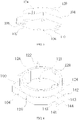
FIG. 1 is an overall assembly view of an inductance device provided in an embodiment of the present invention; -
FIG. 2 is an exploded view of an inductance device provided in an embodiment of the present invention; -
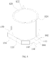
FIG. 3 is a diagonally three-dimensional structural bottom view of a pedestal with a shallow fixing receptacle provided in an embodiment of the present invention; -
FIG. 4 is a diagonally three-dimensional structural top view of a pedestal with a relatively shallow fixing receptacle provided in an embodiment of the present invention; -
FIG. 5 is a diagonally three-dimensional structural top view of a pedestal with a relatively deep fixing receptacle provided in an embodiment of the present invention; -
FIG. 6 is a specific structural view of a main winding part provided in an embodiment of the present invention; -
FIG. 7 is a diagonally three-dimensional structural top view of a pedestal with a square base provided in an embodiment of the present invention; and -
FIG. 8 is a diagonally three-dimensional structural top view of a pedestal with a circular base provided in an embodiment of the present invention. - 1-pedestal, 10-base, 100-bearing surface, 102-fitting surface, 104-side surface, 106-bottom surface, 108-support foot, 12-fixing part/fixing receptacle, 120-wall, 121-bottom, 122-opening, 124-wire passing gap, 126-circumferential limit piece, 128-clasp, 14-auxiliary winding part, 140-welding surface, 141, 142, 144-vertical surface, 143-surface, 145-limit structure/limit groove, 2-main winding part, 20-main winding groove, 22-upper end portion, 220-adsorption surface, 24-lower end portion, 240-circumferential limit matching piece, 26-main body portion, 3-main coil, 4-auxiliary coil.
- In order to make objects, technical details and advantages of the embodiments of the disclosure apparent, the technical solutions of the embodiments will be described in a clearly and fully understandable way in connection with the drawings related to the embodiments of the disclosure. Apparently, the described embodiments are just a part but not all of the embodiments of the disclosure. Based on the described embodiments herein, those skilled in the art can obtain other embodiment(s), without any inventive work, which should be within the scope of the disclosure.
- The technical solutions provided in different embodiments of the present invention are described in detail below with reference to the accompanying drawings.
- An embodiment of the present invention discloses an inductance device, as shown in
FIG. 1 , including a pedestal 1, a main windingpart 2, amain coil 3, and anauxiliary coil 4. - As shown in
FIG. 2 to FIG. 5 , the pedestal 1 includes abase 10, a fixingpart 12, and an auxiliary windingpart 14. The base 10 typically has a flat structure and includes abearing surface 100, afitting surface 102 facing away from the bearingsurface 100, and acircumferential side surface 104 surrounding the bearingsurface 100. A contour defined by theside surface 104 may be square (seeFIG. 7 ), circular (seeFIG. 8 ) or in other regular or irregular shapes (seeFIG. 1 to FIG. 5 ). The fixingpart 12 is typically disposed on one side of the bearingsurface 100. The fixingpart 12 may be fixedly connected to thebearing surface 100 and may also be fixedly connected to theside surface 104 and stretch over the bearingsurface 100. - Referring to
FIG. 1 to FIG. 5 , the fixingpart 12 in this embodiment may be structured as a fixing receptacle or structured in other ways as long as it can fix the main windingpart 12. In this embodiment, a fixing receptacle is described for example. As shown inFIG. 4 andFIG. 5 , the fixing receptacle 12 (the reference numeral of the fixing part is used hereinafter for the convenience of description) in this embodiment is disposed on thebearing surface 100. The fixingreceptacle 12 typically has awall 120, a bottom 121, and anopening 122 defined by thewall 120. A direction from the bottom to the opening is denoted as a first direction a, and thebearing surface 100, thefitting surface 102 and awelding surface 140 are all perpendicular to the first direction a. - The auxiliary winding
part 14 extends away from the base 10 from theside surface 104. - A downward surface of the auxiliary winding
part 14 is thewelding surface 140. The auxiliary windingpart 14 is used for winding anauxiliary coil 4, and the woundauxiliary coil 4 is required to overlay at least a portion of thewelding surface 140 for the convenience of welding. - In this embodiment, the
welding surface 140 and thefitting surface 102 may be flush with each other, and may also have a height difference therebetween, which is similar to a step. But regardless of any structure, in the case that theauxiliary coil 4 is wound around theauxiliary winding part 14, a portion, covering thewelding surface 140, of theauxiliary coil 4 is required to keep flush with or go beyond thefitting surface 102, so that the portion, covering thewelding surface 140, of theauxiliary coil 4 fits on a PCB. - In a solution where a number of auxiliary winding
parts 14 are distributed uniformly, for example, in a solution where four auxiliary windingparts 14 are uniformly distributed on four sides of the base 10 as shown inFIG. 7 , a total area of the portions, covering thewelding surface 140, of theseauxiliary coils 4 is sufficient to make the inductor skeleton structure stably fit on a PCB, the portions, covering thewelding surface 140, of theauxiliary coils 4 can either extend beyond thefitting surface 102 or keep flush with thefitting surface 102 in this solution. - In a solution where there are fewer auxiliary winding parts 14 (e.g.,
FIG. 1 to FIG, 5 , andFIG. 8 ), due to a small area of the portions covering thewelding surface 140 and uneven distribution of theauxiliary coils 4, thewelding surface 140 may be slightly higher than thefitting surface 102, so that the portions, covering thewelding surface 140, of theauxiliary coils 4 and thefitting surface 102 form a substantially flat contact junction surface. - For the above solutions, a variety of different implementations may be adopted. For example, in an implementation shown in
FIG. 3 , thebase 10 has abottom surface 106. Thebottom surface 106 may directly serve as thefitting surface 102. In this case, there is a height difference, like a step, between thewelding surface 140 and thebottom surface 106, so that the portions, covering thewelding surface 140, of theauxiliary coils 4 and thefitting surface 102 form a substantially flat contact junction surface. The structure in such an implementation is complicated and not easy to form. - In another implementation shown in
FIG. 3 , to facilitate the formation of the above-mentioned height difference between thewelding surface 140 and thefitting surface 102, it can be contemplated that thebottom surface 106 is flush with thewelding surface 140 and a plurality ofsupport feet 108 are disposed on thebottom surface 106. An end face, facing away from thebottom surface 106, of each of thesesupport feet 108 will form thefitting surface 102 for contact with a PCB. Thesupport feet 108 are easy to manufacture or dispose for their small size and simple structure. - In this embodiment, there is no particular limitation on the shape of the
auxiliary coil 4 as long as it can overlay a portion of thewelding surface 140. For example, as shown inFIG. 4 andFIG. 5 , the auxiliary coil may be wound circlewise on twovertical surfaces welding surface 140 and asurface 143 on a side, facing the bearingsurface 100, of the auxiliary windingpart 14, and may also be wound on thevertical surfaces vertical surface 144 on one side, facing away from thebase 10, of the auxiliary windingpart 14, or wound in other more complicated ways, which will not be described redundantly here. - To prevent the
auxiliary coil 4 from unwinding from theauxiliary winding part 14, it is desirable to form alimit structure 145 on theauxiliary winding part 14. Thelimit structure 145 is used for constraining theauxiliary coil 4, thereby preventing theauxiliary coil 4 from unwinding from theauxiliary limit part 14. In this embodiment, thelimit structure 145 may be disposed on any surface of the auxiliary windingpart 14. Since theauxiliary coil 4 is integrated, the wholeauxiliary coil 4 may be prevented from unwinding from theauxiliary limit part 14 as long as any portion of theauxiliary coil 4 can be prevented from separation from theauxiliary limit part 14. However, to guarantee the welding effect, thewelding surface 140 may be made as close to a PCB as possible when the inductance device is assembled. Thus, thelimit structure 145 in this embodiment may be disposed on other surface of the auxiliary windingpart 14 than thewelding surface 140. - In this embodiment, the
limit structure 145 may be in the form of a limit stop block, a limit stop plate, and the like, and the form of a limit groove is recommended. The limit groove 145 (the reference numeral of the limit structure is used hereinafter for the convenience of description) is capable of accommodating a portion of theauxiliary coil 4 such that this portion cannot be separated from theauxiliary winding part 14. An extension direction of thelimit groove 145 may be the same as or perpendicular to or even inclined relative to the first direction a. Moreover, there may be more than onelimit grooves 145. For example, thelimit groove 145 may be formed in each of thevertical surfaces limit groove 145 extended in a direction the same as the first direction a may be formed in thevertical surface 141, while thelimit groove 145 extended in a direction perpendicular to the first direction a may be formed in thevertical surface 144. A plurality oflimit grooves 145 are combined to limit the position. A side, facing away from thewelding surface 140, of the auxiliary windingpart 14 is asurface 143. When thelimit groove 145 is formed in thesurface 143, this side may also serve as the bottom of thelimit groove 145. In addition, a plurality of segments oflimit grooves 145 may also be formed in the same surface, which will not be described one by one for example here. - As shown in
FIG. 2 andFIG. 6 , the main windingportion 2 has a main windinggroove 20 for winding amain coil 3. The main windingpart 2 may be designed as a structure of a magnetic core (e.g., the magnetic core of an I-shaped inductance device) without any pin in the prior art. Moreover, the main winding part in this embodiment may be of an integrated magnetic core structure. For example, the main windingpart 2 may include anupper end portion 22, alower end portion 24 and amain body portion 26. Themain body portion 26 is located between theupper end portion 22 and thelower end portion 24. Edges of theupper end portion 22 and thelower end portion 24 are beyond themain body portion 26 and define together with themain body portion 26 the above-mentioned main windinggroove 20. The main windinggroove 20 is used for winding themain coil 3, and theupper end portion 22 and thelower end portion 24 are capable of constraining the form of themain coil 3 and preventing the main coil from unwinding from themain body portion 26. - In this embodiment, the main winding
part 2 is capable of allowing winding of themain coil 3 thereof on the one hand, and on the other hand, can be embedded in the fixingreceptacle 12, so that the main windingpart 2 and the pedestal 1 are combined to form an integrated skeleton structure and are respectively for winding themain coil 3 and theauxiliary coil 4 so as to form the inductance device. The pedestal 1 provides the inductance device with a flat fitting surface for fitting with a PCB. - To facilitate embedding of the main winding
part 2 into the fixingreceptacle 12, thelower end portion 24 may have a shape matching that of the fixingreceptacle 12 so as to extend through theopening 122 and be embedded into the fixingreceptacle 12, and in the case that thelower end portion 24 is embedded in the fixingreceptacle 12, thelower end portion 24, themain body portion 26 and theupper end portion 22 are arranged in sequence in the first direction a. - In this embodiment, when winding the
main coil 3 and theauxiliary coil 4, themain coil 3 and theauxiliary coil 4 may be wound sequentially with the same enameled wire (seeFIG. 2 ); themain coil 3 and theauxiliary coil 4 wound in such a way are electrically connected with one another, and power may be directly supplied to themain coil 3 through theauxiliary coil 4. In addition, themain coil 3 and theauxiliary coil 4 in this embodiment may also be wound with different enameled wires, respectively. In this case, theauxiliary coil 4 is not in electrical connection relationship with themain coil 3, and theauxiliary coil 4 is merely used for fixation during welding. - Since the
main coil 3 is required to have at least one input end and one output end, at least two of theauxiliary coils 4, under normal circumstances, and themain coil 3 are wound with the same enameled wire. The twoauxiliary coils 4 may serve as the input end and the output end of themain coil 3, respectively. As a matter of course, to adapt to different application environments, the number of input ends and that of output ends of themain coil 3 may vary. In this case, the number of theauxiliary coils 4 electrically connected to themain coil 3 may be further increased. - When assembling the inductance device on a PCB, an enamel covering on the portion, covering the
welding surface 140, of eachauxiliary coil 4 is melted at a high temperature to expose a metal wire therein. At the high temperature, the metal wire will be melted and flow to a pad on the PCB. After the melt metal is cooled and solidified, the welding between theauxiliary coil 4 and the pad is completed. Compared with a traditional way of connection through pins, such an assembly way has higher efficiency. Furthermore, since the pad needs not have a region reserved for a pin to pass through in this case, the area of the pad can be greatly reduced and even the pad can be completely hidden under the inductance device, so that the area of the PCB can be greatly reduced. - As shown in
FIG. 1 to FIG. 5 , to improve the stability of assembly, two sides, symmetrical about thebase 10, of the pedestal 1 may both extend to form theauxiliary winding parts 14, and theauxiliary coil 4 is wound around theauxiliary winding part 14 on each side. Thus, during welding, two sides of the inductance device may both be welded to a PCB by means of theauxiliary coils 4, thus resulting in higher stability. The number of the auxiliary windingparts 14 and that of theauxiliary coils 4 may be adjusted according to the desired structural strength and the requirement of electrical connection. Usually, the number of the auxiliary windingparts 14 may be between 2 and 5. - In this embodiment, each
auxiliary coil 4 is typically wound around oneauxiliary winding part 14 individually. However, it is not excluded in this embodiment that theauxiliary coils 4 are all wound around a plurality of auxiliary windingparts 14 on the same side of thebase 10. For example, two auxiliary windingparts 14 on the same side may be used as two support points for theauxiliary coil 4, and an enameled wire is wound around the two auxiliary windingparts 14 to form a strip-shapedauxiliary coil 4. Such anauxiliary coil 4 has a larger welding area with a PCB and thus may have more excellent structural stability and electrical stability. As a matter of course, in addition to the two auxiliary windingparts 14 as support points for winding, theauxiliary coil 4 may further include otherauxiliary winding part 14 in the middle thereof to support in the middle. Thus, a singleauxiliary coil 4 may be wound around two or more auxiliary windingparts 14. - In addition, the enameled wire may be led from the
surface 143 of oneauxiliary winding part 14 to thesurface 143 of another auxiliary windingpart 14 or from thewelding surface 140 of oneauxiliary winding part 14 to thewelding surface 140 of another auxiliary windingpart 14, and may also be led from thesurface 143/thewelding surface 140 of oneauxiliary winding part 14 to thesurface 143/thewelding surface 140 of another auxiliary windingpart 14, thereby forming a single diagonal or cross structure. In addition to the structures described above, in some embodiments, anauxiliary winding part 14 may be lengthened and an enameled wire may be then wound around the lengthenedauxiliary winding part 14 to form a strip-shapedauxiliary coil 4. - When winding an enameled wire to form the
main coil 3, the input end and the output end of themain coil 3 are usually led out from two ends of themain coil 3. The input end and the output end of themain coil 3 are required to extend from the main windinggroove 20 to theauxiliary winding parts 14 for continuously winding theauxiliary coils 4, and in the case that the input end or the output end of themain coil 3 is in a position near thelower end portion 24, it is usually located in the fixingreceptacle 12. In this case, the input end or the output end needs to extend to theauxiliary winding part 14 after passing across theopening 122, which leads to increased difficulty of winding. - Therefore, to facilitate the extending of the enameled wire from the main winding
groove 20 to theauxiliary winding part 14, as shown inFIG. 3 to FIG. 5 , awire passing gap 124 is formed in thewall 120 of the fixingreceptacle 12 in a position corresponding to theauxiliary winding part 14, and thewire passing gap 124 extends to theopening 122 in the first direction a. Thus, each of the input end and the output end of themain coil 3 may pass through thewall 120 directly through thewire passing gap 124 without passing across theopening 122, which reduces difficulty of winding. - For the convenience of manufacturing, the outer contour of the
lower end portion 24 is typically formed into a circular shape. Accordingly, to match thelower end portion 24, the inner contour of the fixingreceptacle 12 is also formed into a circular shape. While such an outer contour is convenient to manufacture, it is easy to cause circumferential rotation of thelower end portion 24 around the center of the circular contour within the fixingreceptacle 12, resulting in loosening and even unwinding of the enameled wire or the coil. To avoid this, as shown inFIG. 4 andFIG. 5 , acircumferential limit piece 126 may be disposed on the fixingreceptacle 12. Meanwhile, as shown inFIG. 6 , a circumferentiallimit matching piece 240 is disposed on thelower end portion 24. The circumferential rotation of thelower end portion 24 around the above-mentioned center within the fixingreceptacle 12 can be limited by means of matching of thecircumferential limit piece 126 and the circumferentiallimit matching piece 240. - In this embodiment, the
circumferential limit piece 126 and the circumferentiallimit matching piece 240 may have any structure that can limit the circumferential rotation, and this embodiment does not have any constraint or use restriction thereon. For example, thecircumferential limit piece 126 may be a limit projection on thewall 120, while the circumferentiallimit matching piece 240 may be a limit notch matching the limit projection. Alternatively, the structure of thecircumferential limit piece 126 may be interchangeable with that of the circumferentiallimit matching piece 240. - In this embodiment, the
circumferential limit piece 126 may be extend to theopening 122 of the fixingreceptacle 12 in the first direction a, while the circumferentiallimit matching piece 240 may extend through two sides of thelower end portion 24 also in the first direction a. Thus, when embedding thelower end portion 24 into the fixingreceptacle 12, thecircumferential limit piece 126 and the circumferentiallimit matching piece 240 may also serve as guiding or positioning element, allowing for smoother embedding. - In this embodiment, a plurality of or a plurality of groups of circumferential limit pieces 126 (two shown in
FIG. 4 andFIG. 5 ) are circumferentially uniformly distributed on the fixingreceptacle 12, while a plurality of or a plurality of groups of circumferentiallimit matching pieces 240 are circumferentially uniformly distributed on thelower end portion 24 correspondingly to thecircumferential limit pieces 126. Since a plurality of or a plurality of groups ofcircumferential limit pieces 126 and circumferentiallimit matching pieces 240 are circumferentially distributed uniformly, thelower end portion 24 and the whole main windingportion 2 may be adjusted circumferentially in angle, so as to enable the input end and the output end of themain coil 3 to be aligned to the respectiveauxiliary winding parts 14, respectively. - In this embodiment, the outer contour of the
lower end portion 24 and the inner contour of the fixingreceptacle 12 may also be non-circular, such as square, triangular, pentagonal and semicircular, and even the cross section of theupper end portion 22 and themain body portion 26 of the main winding part may also be kept in the same configuration with thelower end portion 24. In this case, thecircumferential limit piece 126 and the circumferentiallimit matching piece 240 may be omitted from the main windingpart 2, or it may be construed that thecircumferential limit piece 126 and the circumferentiallimit matching piece 240 have become a portion of the fixingreceptacle 12 and a portion of thelower end portion 24, respectively. - When the
lower end portion 24 is embedded into the fixingreceptacle 12, the fixingreceptacle 12 may be clamped with thelower end portion 24 such that thelower end portion 24 can be tightly connected to the fixingreceptacle 12. Any clamping structure that can realize detachable clamping may be disposed between the fixingreceptacle 12 and thelower end portion 24. For example, as shown inFIG. 4 , aclasp 128 may be disposed in the fixingreceptacle 12. When thelower end portion 24 is embedded into the fixingreceptacle 12, theclasp 128 may be clamped with thelower end portion 24. A bayonet or other structure matching theclasp 128 may be disposed on thelower end portion 24. Alternatively, no any additional structure is added, and theclasp 128 is directly clamped with the side, facing theupper end portion 22, of thelower end portion 24 by spanning over thelower end portion 24 after thelower end portion 24 is embedded in the fixingreceptacle 12. In other embodiments, a clasp might also be disposed on the fixingreceptacle 12, while a bayonet or other matching structure might be disposed on thelower end portion 24. These technical solutions can be implemented by a person skilled in the art according to this embodiment without any effect on the clamping effect. - In this embodiment, the depth (or height) of the fixing
receptacle 12 might also have an impact on the overall performance of the inductance device. For example, to adapt to the surface mount production, an adsorption mechanism needs to be used when transferring the inductance device, and an adsorption surface easy to adsorb needs to be disposed on the inductance device. As shown inFIG. 6 , a side surface, facing away from thelower end portion 24, of theupper end portion 22 is used as aflat adsorption surface 220 in this embodiment. In order not to affect the adsorption effect, the depth (or height) of the fixingreceptacle 12 needs to be limited, so that the fixingreceptacle 12 is not beyond theadsorption surface 220 when thelower end portion 24 is embedded into the fixingreceptacle 12. - In other cases than those described above, the inductance device provided in this embodiment is typically used in an electrical apparatus such as a luminaire. For example, when the inductance device is used in a luminaire, the luminaire typically includes a lamp, a light source module, and a driving module. The lamp typically includes a housing and a front cover. The light source module and the driving module are both disposed on the lamp and electrically connected to each other. The light source module typically includes merely a light source board and a light-emitting diode (LED) chip disposed on the light source board, and the driving module includes a driving board, and a series of components disposed on the driving board, one of which is an inductance device.
- Due to limited space of the luminaire, the components are arranged compactly, and the inductance device is a magnetic component, which might interfere with the normal operation of other components. Therefore, to avoid interference with other components, the fixing
receptacle 12 and even the whole pedestal 1 in this embodiment may be made of a magnetic shielding material such as a magnetic glue and a magnetic ferrite, and the depth (or height) of the fixingreceptacle 12 is limited, so that theupper end portion 22 is not beyond theopening 122 when thelower end portion 24 is embedded into the fixingreceptacle 12. In other words, the main windingpart 2 is completely enclosed by the fixingreceptacle 12. Since the fixingreceptacle 12 is made of a magnetic shielding material, a magnetic field generated by the main windingpart 2 and themain coil 3 can be effectively shielded from interference with other components. - In some luminaires, there might be a case where the light source board and the driving board are integrated. In this case, part of light rays emitted by the LED chip might be thrown on the inductance device. Usually, a magnetic material used for the inductance device has a deep color or even is black with extremely high light absorbance and low reflectance, thus leading to waste of a certain amount of light energy. In this embodiment, the surface of one or even both of the pedestal 1 and the main winding
part 2 may be coated with a light color (e.g., white) to form a reflective surface, thereby providing higher light reflectance. The surface color of the pedestal 1 and the main windingpart 2 may be provided by adjusting the material of the pedestal 1 or the main windingpart 2. Alternatively, the surface of the pedestal 1 and the main windingpart 2 may be coated with a light color pigment. - For the convenience of production, in this embodiment, the
upper end portion 22 and thelower end portion 24 may be structurally symmetrical about themain body portion 26. Thus, theupper end portion 22 and thelower end portion 24 may be arbitrarily interchangeable in position to simplify the winding of the coil and the embedding of the main windingpart 2. - To sum up, the inductor skeleton structure, the inductance device and the luminaire provided in the embodiments of the present invention can be adaptable to the surface mount technology, thereby improving the assembly efficiency.
- The foregoing description of each embodiment of the present invention focuses on the differences from other embodiment. Different optimized features of various embodiments can be combined to derive a better embodiment as long as they do not contradict each other, which will not be reiterated here in consideration of simplicity of wording.
- The foregoing is merely illustrative of the embodiments of the present invention and is not intended to limit the present invention. Various changes and modifications can be made to the present invention by those skilled in the art. Any modifications, equivalent replacements, improvements, etc. made within the spirit and scope of the present invention should be included within the protection scope of the present invention.
Claims (20)
- An inductor skeleton structure, comprising a pedestal and a main winding part,wherein the pedestal comprises a base, a fixing part, and an auxiliary winding part, the fixing part is disposed on the base, the base comprises a downward fitting surface and a circumferential side surface surrounding the fitting surface, and the auxiliary winding part is extended away from the base from the side surface;the main winding part has a main winding groove for winding a main coil; the main winding part is fixed on a side, which is facing away from the fitting surface, of the base by the fixing part; a downward surface of the auxiliary winding part is a welding surface, and the auxiliary winding part is used for winding an auxiliary coil capable of covering at least a portion of the welding surface; andthe welding surface and the fitting surface are configured such that the auxiliary coil covering the welding surface is flush with the fitting surface or beyond the fitting surface.
- The inductor skeleton structure according to claim 1, wherein the side, which is facing away from the fitting surface, of the base is a bearing surface, and the fixing part is disposed on the bearing surface;
the fixing part is a fixing receptacle, and the main winding part is capable of being embedded in the fixing receptacle; the fixing receptacle comprises a bottom, a wall, and an opening defined by the wall; a direction from the bottom to the opening is denoted as a first direction, and the bearing surface, the fitting surface and the welding surface are all perpendicular to the first direction. - The inductor skeleton structure according to claim 2, wherein the main winding part comprises an upper end portion, a lower end portion and a main body portion, the main body portion is between the upper end portion and the lower end portion, and edges of both the upper end portion and the lower end portion are beyond the main body portion and define together with the main body portion the main winding groove;
the lower end portion is in a shape matching a shape of the fixing receptacle and is capable of being embedded in the fixing receptacle, and in a case that the lower end portion is embedded in the fixing receptacle, the lower end portion, the main body portion and the upper end portion are arranged in sequence along the first direction. - The inductor skeleton structure according to claim 3, wherein an inner contour of the fixing receptacle and an outer contour of the lower end portion are both in a circular shape, a circumferential limit piece is disposed on the fixing receptacle, and a circumferential limit matching piece is disposed on the lower end portion; and the lower end portion and the fixing receptacle are capable of being limited from rotation around a center of the circular shape by matching of the circumferential limit piece and the circumferential limit matching piece.
- The inductor skeleton structure according to claim 4, wherein the circumferential limit piece is a limit projection on the wall, and the circumferential limit matching piece is a limit notch matching the limit projection; and
the circumferential limit piece is extended to the opening along the first direction, and the circumferential limit matching piece is extended through two sides of the lower end portion along the first direction. - The inductor skeleton structure according to any one of claims 4 and 5, wherein a plurality of or a plurality of groups of circumferential limit pieces are circumferentially uniformly distributed on the fixing receptacle, and a plurality of or a plurality of groups of circumferential limit matching pieces are circumferentially uniformly distributed on the lower end portion corresponding to the circumferential limit pieces.
- The inductor skeleton structure according to any one of claims 3 to 5, wherein a side surface, which is facing away from the lower end portion, of the upper end portion is a flat adsorption surface; and in a case that the lower end portion is embedded in the fixing receptacle, the fixing receptacle is not beyond the adsorption surface.
- The inductor skeleton structure according to any one of claims 3 to 5, wherein the fixing receptacle is formed of a magnetic shielding material; in the case that the lower end portion is embedded in the fixing receptacle, the upper end portion is not beyond the opening of the fixing receptacle; and
the upper end portion and the lower end portion are structurally symmetrical about the main body portion. - The inductor skeleton structure according to any one of claims 3 to 5, wherein in the case that the lower end portion is embedded in the fixing receptacle, the fixing receptacle is clamped with the lower end portion.
- The inductor skeleton structure according to any one of claims 2 to 5, wherein a wire passing gap is formed in the wall in a position corresponding to the auxiliary winding part, and the wire passing gap is extended to the opening of the fixing receptacle along the first direction.
- The inductor skeleton structure according to any one of claims 1 to 5, wherein the base has a bottom surface which serves as the fitting surface; the bottom surface is higher than the welding surface and a height difference between the bottom surface and the welding surface enables the auxiliary coil covering the welding surface to be flush with the fitting surface;
alternatively, the base has a bottom surface which is flush with the welding surface; a plurality of support feet are disposed on the bottom surface; and an end face, which is facing away from the bottom surface, of each of plurality of support feet forms the fitting surface. - The inductor skeleton structure according to any one of claims 1 to 5, wherein a limit structure is further disposed on the auxiliary winding part to prevent the auxiliary coil wound around the auxiliary limit part from unwinding from the auxiliary winding part.
- The inductor skeleton structure according to claim 12, wherein the limit structure is a limit groove for accommodating a portion of the auxiliary coil; an extension direction of the limit groove is same as and/or perpendicular to the first direction; and each of two sides, which are symmetrical about the fixing receptacle, of the base is extended to form the auxiliary winding part.
- The inductor skeleton structure according to any one of claims 1 to 5, wherein a surface of the pedestal and/or the main winding part is a reflective surface.
- An inductance device, comprising the inductor skeleton structure according to any one of claims 1 to 21, the main coil, and the auxiliary coil,
wherein the main coil is wound within the main winding groove, and the auxiliary coil is wound around the auxiliary winding part and covers the portion of the welding surface. - The inductance device according to claim 15, wherein the main coil and the auxiliary coil are wound with a single enameled wire or different enameled wires.
- The inductance device according to claim 16, wherein a count of the auxiliary coil is at least two, and the main coil and the at least two auxiliary coils are wound with a single enameled wire.
- The inductance device according to claim 17, wherein at least one of the auxiliary coils is individually wound around one auxiliary winding part;
alternatively, at least one of the auxiliary coils is wound around a plurality of auxiliary winding parts on a same side of the base. - A luminaire, comprising a lamp, a light source module and a driving module,
wherein the light source module and the driving module are both disposed on the lamp and electrically connected to each other; the driving module comprises a driving board; and the inductance device according to any one of claims 22 to 26 is disposed on the driving board. - The luminaire according to claim 19, wherein the light source module comprises a light source board which is integrated with the driving board; and a surface of the pedestal and/or the main winding part is a reflective surface.
Applications Claiming Priority (3)
| Application Number | Priority Date | Filing Date | Title |
|---|---|---|---|
| CN201910846720.2A CN110534320B (en) | 2019-09-09 | 2019-09-09 | Inductance skeleton texture, inductance device and lamps and lanterns |
| CN201921493365.7U CN210325481U (en) | 2019-09-09 | 2019-09-09 | Inductive skeleton structure, inductive device and lamps |
| PCT/CN2020/112838 WO2021047422A1 (en) | 2019-09-09 | 2020-09-01 | Inductor framework structure, inductor device and lamp |
Publications (3)
| Publication Number | Publication Date |
|---|---|
| EP3975209A1 true EP3975209A1 (en) | 2022-03-30 |
| EP3975209A4 EP3975209A4 (en) | 2022-09-14 |
| EP3975209B1 EP3975209B1 (en) | 2025-04-30 |
Family
ID=74866561
Family Applications (1)
| Application Number | Title | Priority Date | Filing Date |
|---|---|---|---|
| EP20862602.8A Active EP3975209B1 (en) | 2019-09-09 | 2020-09-01 | Inductor framework structure, inductor device and lamp |
Country Status (3)
| Country | Link |
|---|---|
| US (1) | US12451285B2 (en) |
| EP (1) | EP3975209B1 (en) |
| WO (1) | WO2021047422A1 (en) |
Families Citing this family (5)
| Publication number | Priority date | Publication date | Assignee | Title |
|---|---|---|---|---|
| WO2020020106A1 (en) * | 2018-07-23 | 2020-01-30 | 苏州欧普照明有限公司 | Inductor core and inductor device |
| CN117038285A (en) * | 2023-07-20 | 2023-11-10 | 广东群硕电子技术有限公司 | Inductor and method of manufacturing inductor |
| CN117174432B (en) * | 2023-09-11 | 2024-08-06 | 惠州市英达特电子技术有限公司 | A fluid magnetic integrated inductor |
| CN119092278B (en) * | 2024-11-05 | 2025-02-07 | 于都县亚星电子科技有限公司 | Plug-in type transformer skeleton and transformer |
| CN120126894A (en) * | 2025-02-13 | 2025-06-10 | 深圳市鸿富邦科技有限公司 | A high performance manganese zinc SMD chip inductor and its production process |
Family Cites Families (13)
| Publication number | Priority date | Publication date | Assignee | Title |
|---|---|---|---|---|
| JPH06260342A (en) * | 1993-03-09 | 1994-09-16 | Taiyo Yuden Co Ltd | Surface-mount type coil component |
| JPH0799124A (en) * | 1993-09-28 | 1995-04-11 | Taiyo Yuden Co Ltd | Surface mounting coil |
| JP3497276B2 (en) * | 1994-07-20 | 2004-02-16 | 松下電器産業株式会社 | Inductance element and manufacturing method thereof |
| TW499030U (en) * | 2000-08-18 | 2002-08-11 | Delta Electronics Inc | Base structure of the surface mount inductor |
| DE10124378A1 (en) * | 2001-05-18 | 2002-11-21 | Pemetzrieder Neosid | Inductive miniature component for surface mounting has electrically conducting metallised wire winding of larger diameter than coil winding wire between journals, coil winding wire ends |
| KR101187970B1 (en) * | 2010-12-21 | 2012-10-05 | 삼성전기주식회사 | Planar transformer, and driver having thereof and display apparatus |
| CN102537781B (en) * | 2011-12-09 | 2013-07-31 | 东莞勤上光电股份有限公司 | Led lamp |
| CN203366953U (en) * | 2013-07-18 | 2013-12-25 | 广安市华蓥山领创电子有限公司 | Ultra-thin inductance framework |
| CN208352091U (en) * | 2018-06-20 | 2019-01-08 | 深圳市高斯博电子科技有限公司 | A kind of high power inductors of composite magnetic circuit |
| CN108831715A (en) * | 2018-07-23 | 2018-11-16 | 苏州欧普照明有限公司 | inductance framework and inductance device |
| CN110120295B (en) * | 2019-06-05 | 2024-07-02 | 深圳市京泉华科技股份有限公司 | Common-mode inductor, common-mode inductor winding jig and common-mode inductor winding method |
| CN210325481U (en) * | 2019-09-09 | 2020-04-14 | 苏州欧普照明有限公司 | Inductive skeleton structure, inductive device and lamps |
| CN110534320B (en) * | 2019-09-09 | 2024-07-30 | 苏州欧普照明有限公司 | Inductance skeleton texture, inductance device and lamps and lanterns |
-
2020
- 2020-09-01 EP EP20862602.8A patent/EP3975209B1/en active Active
- 2020-09-01 WO PCT/CN2020/112838 patent/WO2021047422A1/en not_active Ceased
-
2021
- 2021-12-27 US US17/563,003 patent/US12451285B2/en active Active
Also Published As
| Publication number | Publication date |
|---|---|
| US12451285B2 (en) | 2025-10-21 |
| WO2021047422A1 (en) | 2021-03-18 |
| EP3975209A4 (en) | 2022-09-14 |
| US20220122759A1 (en) | 2022-04-21 |
| EP3975209B1 (en) | 2025-04-30 |
Similar Documents
| Publication | Publication Date | Title |
|---|---|---|
| EP3975209B1 (en) | Inductor framework structure, inductor device and lamp | |
| CN110139477A (en) | Power module and power module package assembly applied to intelligent terminal | |
| KR101124003B1 (en) | Transformer and flat panel display device using the same | |
| JP2011119206A (en) | Led lighting device | |
| KR20130008655A (en) | Transformer and display device using the same | |
| US12392484B1 (en) | Decorative light string | |
| TWM526169U (en) | Transformer seat and electronic device using the same | |
| WO2021047421A1 (en) | Inductance frame, inductance apparatus and light fixture | |
| KR101647721B1 (en) | Inductor And Method Of Fabricating The Same | |
| WO2022166857A1 (en) | Inductor and electrical component including same | |
| CN110517863A (en) | Inductance framework and inductance device | |
| CN105627171A (en) | Optical element, light sources module and lighting device | |
| JP2013534715A (en) | Transformer and switch power supply and LED fluorescent lamp using the transformer | |
| EP3979274B1 (en) | Inductive framework, inductive device, and lamp | |
| CN208507408U (en) | Small size ultra-thin transformer | |
| JP2018133221A (en) | Lighting device | |
| CN210325481U (en) | Inductive skeleton structure, inductive device and lamps | |
| KR20120138700A (en) | Transformer and display device using the same | |
| CN110534320B (en) | Inductance skeleton texture, inductance device and lamps and lanterns | |
| JP3818979B2 (en) | Leakage transformer | |
| CN205402340U (en) | Optical element , light source module and lighting device | |
| CN206330011U (en) | A kind of light source module and lighting device | |
| CN210668053U (en) | Inductive bobbins, inductive devices and lamps | |
| EP3800652B1 (en) | Inductance device | |
| CN210272031U (en) | Inductive bobbins, inductive devices and lamps |
Legal Events
| Date | Code | Title | Description |
|---|---|---|---|
| STAA | Information on the status of an ep patent application or granted ep patent |
Free format text: STATUS: THE INTERNATIONAL PUBLICATION HAS BEEN MADE |
|
| PUAI | Public reference made under article 153(3) epc to a published international application that has entered the european phase |
Free format text: ORIGINAL CODE: 0009012 |
|
| STAA | Information on the status of an ep patent application or granted ep patent |
Free format text: STATUS: REQUEST FOR EXAMINATION WAS MADE |
|
| 17P | Request for examination filed |
Effective date: 20211222 |
|
| AK | Designated contracting states |
Kind code of ref document: A1 Designated state(s): AL AT BE BG CH CY CZ DE DK EE ES FI FR GB GR HR HU IE IS IT LI LT LU LV MC MK MT NL NO PL PT RO RS SE SI SK SM TR |
|
| REG | Reference to a national code |
Ref country code: DE Ref legal event code: R079 Free format text: PREVIOUS MAIN CLASS: H01F0027300000 Ipc: H01F0027280000 Ref country code: DE Ref legal event code: R079 Ref document number: 602020050584 Country of ref document: DE Free format text: PREVIOUS MAIN CLASS: H01F0027300000 Ipc: H01F0027280000 |
|
| A4 | Supplementary search report drawn up and despatched |
Effective date: 20220816 |
|
| RIC1 | Information provided on ipc code assigned before grant |
Ipc: H01F 27/29 20060101ALI20220809BHEP Ipc: H01F 27/26 20060101ALI20220809BHEP Ipc: H01F 17/04 20060101ALI20220809BHEP Ipc: F21V 23/02 20060101ALI20220809BHEP Ipc: H01F 27/28 20060101AFI20220809BHEP |
|
| DAV | Request for validation of the european patent (deleted) | ||
| DAX | Request for extension of the european patent (deleted) | ||
| GRAP | Despatch of communication of intention to grant a patent |
Free format text: ORIGINAL CODE: EPIDOSNIGR1 |
|
| STAA | Information on the status of an ep patent application or granted ep patent |
Free format text: STATUS: GRANT OF PATENT IS INTENDED |
|
| INTG | Intention to grant announced |
Effective date: 20241220 |
|
| GRAS | Grant fee paid |
Free format text: ORIGINAL CODE: EPIDOSNIGR3 |
|
| GRAA | (expected) grant |
Free format text: ORIGINAL CODE: 0009210 |
|
| STAA | Information on the status of an ep patent application or granted ep patent |
Free format text: STATUS: THE PATENT HAS BEEN GRANTED |
|
| AK | Designated contracting states |
Kind code of ref document: B1 Designated state(s): AL AT BE BG CH CY CZ DE DK EE ES FI FR GB GR HR HU IE IS IT LI LT LU LV MC MK MT NL NO PL PT RO RS SE SI SK SM TR |
|
| REG | Reference to a national code |
Ref country code: CH Ref legal event code: EP Ref country code: GB Ref legal event code: FG4D |
|
| REG | Reference to a national code |
Ref country code: IE Ref legal event code: FG4D |
|
| REG | Reference to a national code |
Ref country code: DE Ref legal event code: R096 Ref document number: 602020050584 Country of ref document: DE |
|
| REG | Reference to a national code |
Ref country code: NL Ref legal event code: FP |
|
| REG | Reference to a national code |
Ref country code: AT Ref legal event code: MK05 Ref document number: 1790869 Country of ref document: AT Kind code of ref document: T Effective date: 20250430 |
|
| PG25 | Lapsed in a contracting state [announced via postgrant information from national office to epo] |
Ref country code: PT Free format text: LAPSE BECAUSE OF FAILURE TO SUBMIT A TRANSLATION OF THE DESCRIPTION OR TO PAY THE FEE WITHIN THE PRESCRIBED TIME-LIMIT Effective date: 20250901 Ref country code: ES Free format text: LAPSE BECAUSE OF FAILURE TO SUBMIT A TRANSLATION OF THE DESCRIPTION OR TO PAY THE FEE WITHIN THE PRESCRIBED TIME-LIMIT Effective date: 20250430 Ref country code: FI Free format text: LAPSE BECAUSE OF FAILURE TO SUBMIT A TRANSLATION OF THE DESCRIPTION OR TO PAY THE FEE WITHIN THE PRESCRIBED TIME-LIMIT Effective date: 20250430 |
|
| PGFP | Annual fee paid to national office [announced via postgrant information from national office to epo] |
Ref country code: DE Payment date: 20250916 Year of fee payment: 6 |
|
| REG | Reference to a national code |
Ref country code: LT Ref legal event code: MG9D |
|
| PG25 | Lapsed in a contracting state [announced via postgrant information from national office to epo] |
Ref country code: GR Free format text: LAPSE BECAUSE OF FAILURE TO SUBMIT A TRANSLATION OF THE DESCRIPTION OR TO PAY THE FEE WITHIN THE PRESCRIBED TIME-LIMIT Effective date: 20250731 Ref country code: NO Free format text: LAPSE BECAUSE OF FAILURE TO SUBMIT A TRANSLATION OF THE DESCRIPTION OR TO PAY THE FEE WITHIN THE PRESCRIBED TIME-LIMIT Effective date: 20250730 |
|
| PG25 | Lapsed in a contracting state [announced via postgrant information from national office to epo] |
Ref country code: PL Free format text: LAPSE BECAUSE OF FAILURE TO SUBMIT A TRANSLATION OF THE DESCRIPTION OR TO PAY THE FEE WITHIN THE PRESCRIBED TIME-LIMIT Effective date: 20250430 |
|
| PGFP | Annual fee paid to national office [announced via postgrant information from national office to epo] |
Ref country code: NL Payment date: 20250909 Year of fee payment: 6 |
|
| PG25 | Lapsed in a contracting state [announced via postgrant information from national office to epo] |
Ref country code: BG Free format text: LAPSE BECAUSE OF FAILURE TO SUBMIT A TRANSLATION OF THE DESCRIPTION OR TO PAY THE FEE WITHIN THE PRESCRIBED TIME-LIMIT Effective date: 20250430 |
|
| PGFP | Annual fee paid to national office [announced via postgrant information from national office to epo] |
Ref country code: BE Payment date: 20250919 Year of fee payment: 6 Ref country code: GB Payment date: 20250919 Year of fee payment: 6 |
|
| PG25 | Lapsed in a contracting state [announced via postgrant information from national office to epo] |
Ref country code: HR Free format text: LAPSE BECAUSE OF FAILURE TO SUBMIT A TRANSLATION OF THE DESCRIPTION OR TO PAY THE FEE WITHIN THE PRESCRIBED TIME-LIMIT Effective date: 20250430 |
|
| PG25 | Lapsed in a contracting state [announced via postgrant information from national office to epo] |
Ref country code: AT Free format text: LAPSE BECAUSE OF FAILURE TO SUBMIT A TRANSLATION OF THE DESCRIPTION OR TO PAY THE FEE WITHIN THE PRESCRIBED TIME-LIMIT Effective date: 20250430 |
|
| PGFP | Annual fee paid to national office [announced via postgrant information from national office to epo] |
Ref country code: FR Payment date: 20250929 Year of fee payment: 6 |
|
| PG25 | Lapsed in a contracting state [announced via postgrant information from national office to epo] |
Ref country code: RS Free format text: LAPSE BECAUSE OF FAILURE TO SUBMIT A TRANSLATION OF THE DESCRIPTION OR TO PAY THE FEE WITHIN THE PRESCRIBED TIME-LIMIT Effective date: 20250731 |
|
| PG25 | Lapsed in a contracting state [announced via postgrant information from national office to epo] |
Ref country code: IS Free format text: LAPSE BECAUSE OF FAILURE TO SUBMIT A TRANSLATION OF THE DESCRIPTION OR TO PAY THE FEE WITHIN THE PRESCRIBED TIME-LIMIT Effective date: 20250830 |
|
| PG25 | Lapsed in a contracting state [announced via postgrant information from national office to epo] |
Ref country code: LV Free format text: LAPSE BECAUSE OF FAILURE TO SUBMIT A TRANSLATION OF THE DESCRIPTION OR TO PAY THE FEE WITHIN THE PRESCRIBED TIME-LIMIT Effective date: 20250430 |
|
| PG25 | Lapsed in a contracting state [announced via postgrant information from national office to epo] |
Ref country code: SM Free format text: LAPSE BECAUSE OF FAILURE TO SUBMIT A TRANSLATION OF THE DESCRIPTION OR TO PAY THE FEE WITHIN THE PRESCRIBED TIME-LIMIT Effective date: 20250430 Ref country code: DK Free format text: LAPSE BECAUSE OF FAILURE TO SUBMIT A TRANSLATION OF THE DESCRIPTION OR TO PAY THE FEE WITHIN THE PRESCRIBED TIME-LIMIT Effective date: 20250430 |
|
| PG25 | Lapsed in a contracting state [announced via postgrant information from national office to epo] |
Ref country code: CZ Free format text: LAPSE BECAUSE OF FAILURE TO SUBMIT A TRANSLATION OF THE DESCRIPTION OR TO PAY THE FEE WITHIN THE PRESCRIBED TIME-LIMIT Effective date: 20250430 |
|
| PG25 | Lapsed in a contracting state [announced via postgrant information from national office to epo] |
Ref country code: EE Free format text: LAPSE BECAUSE OF FAILURE TO SUBMIT A TRANSLATION OF THE DESCRIPTION OR TO PAY THE FEE WITHIN THE PRESCRIBED TIME-LIMIT Effective date: 20250430 |
|
| PG25 | Lapsed in a contracting state [announced via postgrant information from national office to epo] |
Ref country code: RO Free format text: LAPSE BECAUSE OF FAILURE TO SUBMIT A TRANSLATION OF THE DESCRIPTION OR TO PAY THE FEE WITHIN THE PRESCRIBED TIME-LIMIT Effective date: 20250430 Ref country code: SK Free format text: LAPSE BECAUSE OF FAILURE TO SUBMIT A TRANSLATION OF THE DESCRIPTION OR TO PAY THE FEE WITHIN THE PRESCRIBED TIME-LIMIT Effective date: 20250430 |
|
| PG25 | Lapsed in a contracting state [announced via postgrant information from national office to epo] |
Ref country code: IT Free format text: LAPSE BECAUSE OF FAILURE TO SUBMIT A TRANSLATION OF THE DESCRIPTION OR TO PAY THE FEE WITHIN THE PRESCRIBED TIME-LIMIT Effective date: 20250430 |
|
| REG | Reference to a national code |
Ref country code: DE Ref legal event code: R097 Ref document number: 602020050584 Country of ref document: DE |
|
| PLBE | No opposition filed within time limit |
Free format text: ORIGINAL CODE: 0009261 |
|
| STAA | Information on the status of an ep patent application or granted ep patent |
Free format text: STATUS: NO OPPOSITION FILED WITHIN TIME LIMIT |
|
| REG | Reference to a national code |
Ref country code: CH Ref legal event code: L10 Free format text: ST27 STATUS EVENT CODE: U-0-0-L10-L00 (AS PROVIDED BY THE NATIONAL OFFICE) Effective date: 20260311 |
|
| 26N | No opposition filed |
Effective date: 20260202 |
|
| REG | Reference to a national code |
Ref country code: CH Ref legal event code: H13 Free format text: ST27 STATUS EVENT CODE: U-0-0-H10-H13 (AS PROVIDED BY THE NATIONAL OFFICE) Effective date: 20260504 |