EP3972063A1 - Silicon-photonics-based semiconductor optical amplifier with n-doped active layer - Google Patents
Silicon-photonics-based semiconductor optical amplifier with n-doped active layer Download PDFInfo
- Publication number
- EP3972063A1 EP3972063A1 EP21197432.4A EP21197432A EP3972063A1 EP 3972063 A1 EP3972063 A1 EP 3972063A1 EP 21197432 A EP21197432 A EP 21197432A EP 3972063 A1 EP3972063 A1 EP 3972063A1
- Authority
- EP
- European Patent Office
- Prior art keywords
- layer
- optical amplifier
- active layer
- semiconductor optical
- gain medium
- Prior art date
- Legal status (The legal status is an assumption and is not a legal conclusion. Google has not performed a legal analysis and makes no representation as to the accuracy of the status listed.)
- Pending
Links
Images


Classifications
-
- H—ELECTRICITY
- H01—ELECTRIC ELEMENTS
- H01S—DEVICES USING THE PROCESS OF LIGHT AMPLIFICATION BY STIMULATED EMISSION OF RADIATION [LASER] TO AMPLIFY OR GENERATE LIGHT; DEVICES USING STIMULATED EMISSION OF ELECTROMAGNETIC RADIATION IN WAVE RANGES OTHER THAN OPTICAL
- H01S5/00—Semiconductor lasers
- H01S5/02—Structural details or components not essential to laser action
- H01S5/026—Monolithically integrated components, e.g. waveguides, monitoring photo-detectors, drivers
-
- H—ELECTRICITY
- H01—ELECTRIC ELEMENTS
- H01S—DEVICES USING THE PROCESS OF LIGHT AMPLIFICATION BY STIMULATED EMISSION OF RADIATION [LASER] TO AMPLIFY OR GENERATE LIGHT; DEVICES USING STIMULATED EMISSION OF ELECTROMAGNETIC RADIATION IN WAVE RANGES OTHER THAN OPTICAL
- H01S5/00—Semiconductor lasers
- H01S5/02—Structural details or components not essential to laser action
- H01S5/028—Coatings ; Treatment of the laser facets, e.g. etching, passivation layers or reflecting layers
-
- H—ELECTRICITY
- H01—ELECTRIC ELEMENTS
- H01S—DEVICES USING THE PROCESS OF LIGHT AMPLIFICATION BY STIMULATED EMISSION OF RADIATION [LASER] TO AMPLIFY OR GENERATE LIGHT; DEVICES USING STIMULATED EMISSION OF ELECTROMAGNETIC RADIATION IN WAVE RANGES OTHER THAN OPTICAL
- H01S5/00—Semiconductor lasers
- H01S5/02—Structural details or components not essential to laser action
- H01S5/028—Coatings ; Treatment of the laser facets, e.g. etching, passivation layers or reflecting layers
- H01S5/0287—Facet reflectivity
-
- H—ELECTRICITY
- H01—ELECTRIC ELEMENTS
- H01S—DEVICES USING THE PROCESS OF LIGHT AMPLIFICATION BY STIMULATED EMISSION OF RADIATION [LASER] TO AMPLIFY OR GENERATE LIGHT; DEVICES USING STIMULATED EMISSION OF ELECTROMAGNETIC RADIATION IN WAVE RANGES OTHER THAN OPTICAL
- H01S5/00—Semiconductor lasers
- H01S5/06—Arrangements for controlling the laser output parameters, e.g. by operating on the active medium
- H01S5/068—Stabilisation of laser output parameters
-
- H—ELECTRICITY
- H01—ELECTRIC ELEMENTS
- H01S—DEVICES USING THE PROCESS OF LIGHT AMPLIFICATION BY STIMULATED EMISSION OF RADIATION [LASER] TO AMPLIFY OR GENERATE LIGHT; DEVICES USING STIMULATED EMISSION OF ELECTROMAGNETIC RADIATION IN WAVE RANGES OTHER THAN OPTICAL
- H01S5/00—Semiconductor lasers
- H01S5/10—Construction or shape of the optical resonator, e.g. extended or external cavity, coupled cavities, bent-guide, varying width, thickness or composition of the active region
- H01S5/14—External cavity lasers
- H01S5/141—External cavity lasers using a wavelength selective device, e.g. a grating or etalon
- H01S5/142—External cavity lasers using a wavelength selective device, e.g. a grating or etalon which comprises an additional resonator
-
- H—ELECTRICITY
- H01—ELECTRIC ELEMENTS
- H01S—DEVICES USING THE PROCESS OF LIGHT AMPLIFICATION BY STIMULATED EMISSION OF RADIATION [LASER] TO AMPLIFY OR GENERATE LIGHT; DEVICES USING STIMULATED EMISSION OF ELECTROMAGNETIC RADIATION IN WAVE RANGES OTHER THAN OPTICAL
- H01S5/00—Semiconductor lasers
- H01S5/30—Structure or shape of the active region; Materials used for the active region
- H01S5/305—Structure or shape of the active region; Materials used for the active region characterised by the doping materials used in the laser structure
- H01S5/3086—Structure or shape of the active region; Materials used for the active region characterised by the doping materials used in the laser structure doping of the active layer
- H01S5/309—Structure or shape of the active region; Materials used for the active region characterised by the doping materials used in the laser structure doping of the active layer doping of barrier layers that confine charge carriers in the laser structure, e.g. the barriers in a quantum well structure
-
- H—ELECTRICITY
- H01—ELECTRIC ELEMENTS
- H01S—DEVICES USING THE PROCESS OF LIGHT AMPLIFICATION BY STIMULATED EMISSION OF RADIATION [LASER] TO AMPLIFY OR GENERATE LIGHT; DEVICES USING STIMULATED EMISSION OF ELECTROMAGNETIC RADIATION IN WAVE RANGES OTHER THAN OPTICAL
- H01S5/00—Semiconductor lasers
- H01S5/50—Amplifier structures not provided for in groups H01S5/02 - H01S5/30
-
- H—ELECTRICITY
- H01—ELECTRIC ELEMENTS
- H01S—DEVICES USING THE PROCESS OF LIGHT AMPLIFICATION BY STIMULATED EMISSION OF RADIATION [LASER] TO AMPLIFY OR GENERATE LIGHT; DEVICES USING STIMULATED EMISSION OF ELECTROMAGNETIC RADIATION IN WAVE RANGES OTHER THAN OPTICAL
- H01S5/00—Semiconductor lasers
- H01S5/005—Optical components external to the laser cavity, specially adapted therefor, e.g. for homogenisation or merging of the beams or for manipulating laser pulses, e.g. pulse shaping
- H01S5/0078—Optical components external to the laser cavity, specially adapted therefor, e.g. for homogenisation or merging of the beams or for manipulating laser pulses, e.g. pulse shaping for frequency filtering
-
- H—ELECTRICITY
- H01—ELECTRIC ELEMENTS
- H01S—DEVICES USING THE PROCESS OF LIGHT AMPLIFICATION BY STIMULATED EMISSION OF RADIATION [LASER] TO AMPLIFY OR GENERATE LIGHT; DEVICES USING STIMULATED EMISSION OF ELECTROMAGNETIC RADIATION IN WAVE RANGES OTHER THAN OPTICAL
- H01S5/00—Semiconductor lasers
- H01S5/02—Structural details or components not essential to laser action
- H01S5/0206—Substrates, e.g. growth, shape, material, removal or bonding
- H01S5/021—Silicon based substrates
-
- H—ELECTRICITY
- H01—ELECTRIC ELEMENTS
- H01S—DEVICES USING THE PROCESS OF LIGHT AMPLIFICATION BY STIMULATED EMISSION OF RADIATION [LASER] TO AMPLIFY OR GENERATE LIGHT; DEVICES USING STIMULATED EMISSION OF ELECTROMAGNETIC RADIATION IN WAVE RANGES OTHER THAN OPTICAL
- H01S5/00—Semiconductor lasers
- H01S5/02—Structural details or components not essential to laser action
- H01S5/0206—Substrates, e.g. growth, shape, material, removal or bonding
- H01S5/0218—Substrates comprising semiconducting materials from other groups of the Periodic Table than the materials of the active layer
-
- H—ELECTRICITY
- H01—ELECTRIC ELEMENTS
- H01S—DEVICES USING THE PROCESS OF LIGHT AMPLIFICATION BY STIMULATED EMISSION OF RADIATION [LASER] TO AMPLIFY OR GENERATE LIGHT; DEVICES USING STIMULATED EMISSION OF ELECTROMAGNETIC RADIATION IN WAVE RANGES OTHER THAN OPTICAL
- H01S5/00—Semiconductor lasers
- H01S5/10—Construction or shape of the optical resonator, e.g. extended or external cavity, coupled cavities, bent-guide, varying width, thickness or composition of the active region
- H01S5/1003—Waveguide having a modified shape along the axis, e.g. branched, curved, tapered, voids
- H01S5/101—Curved waveguide
-
- H—ELECTRICITY
- H01—ELECTRIC ELEMENTS
- H01S—DEVICES USING THE PROCESS OF LIGHT AMPLIFICATION BY STIMULATED EMISSION OF RADIATION [LASER] TO AMPLIFY OR GENERATE LIGHT; DEVICES USING STIMULATED EMISSION OF ELECTROMAGNETIC RADIATION IN WAVE RANGES OTHER THAN OPTICAL
- H01S5/00—Semiconductor lasers
- H01S5/10—Construction or shape of the optical resonator, e.g. extended or external cavity, coupled cavities, bent-guide, varying width, thickness or composition of the active region
- H01S5/1039—Details on the cavity length
-
- H—ELECTRICITY
- H01—ELECTRIC ELEMENTS
- H01S—DEVICES USING THE PROCESS OF LIGHT AMPLIFICATION BY STIMULATED EMISSION OF RADIATION [LASER] TO AMPLIFY OR GENERATE LIGHT; DEVICES USING STIMULATED EMISSION OF ELECTROMAGNETIC RADIATION IN WAVE RANGES OTHER THAN OPTICAL
- H01S5/00—Semiconductor lasers
- H01S5/10—Construction or shape of the optical resonator, e.g. extended or external cavity, coupled cavities, bent-guide, varying width, thickness or composition of the active region
- H01S5/1082—Construction or shape of the optical resonator, e.g. extended or external cavity, coupled cavities, bent-guide, varying width, thickness or composition of the active region with a special facet structure, e.g. structured, non planar, oblique
- H01S5/1085—Oblique facets
-
- H—ELECTRICITY
- H01—ELECTRIC ELEMENTS
- H01S—DEVICES USING THE PROCESS OF LIGHT AMPLIFICATION BY STIMULATED EMISSION OF RADIATION [LASER] TO AMPLIFY OR GENERATE LIGHT; DEVICES USING STIMULATED EMISSION OF ELECTROMAGNETIC RADIATION IN WAVE RANGES OTHER THAN OPTICAL
- H01S5/00—Semiconductor lasers
- H01S5/20—Structure or shape of the semiconductor body to guide the optical wave ; Confining structures perpendicular to the optical axis, e.g. index or gain guiding, stripe geometry, broad area lasers, gain tailoring, transverse or lateral reflectors, special cladding structures, MQW barrier reflection layers
- H01S5/2004—Confining in the direction perpendicular to the layer structure
- H01S5/2018—Optical confinement, e.g. absorbing-, reflecting- or waveguide-layers
- H01S5/2031—Optical confinement, e.g. absorbing-, reflecting- or waveguide-layers characterized by special waveguide layers, e.g. asymmetric waveguide layers or defined bandgap discontinuities
-
- H—ELECTRICITY
- H01—ELECTRIC ELEMENTS
- H01S—DEVICES USING THE PROCESS OF LIGHT AMPLIFICATION BY STIMULATED EMISSION OF RADIATION [LASER] TO AMPLIFY OR GENERATE LIGHT; DEVICES USING STIMULATED EMISSION OF ELECTROMAGNETIC RADIATION IN WAVE RANGES OTHER THAN OPTICAL
- H01S5/00—Semiconductor lasers
- H01S5/30—Structure or shape of the active region; Materials used for the active region
- H01S5/32—Structure or shape of the active region; Materials used for the active region comprising PN junctions, e.g. hetero- or double- heterostructures
- H01S5/3211—Structure or shape of the active region; Materials used for the active region comprising PN junctions, e.g. hetero- or double- heterostructures characterised by special cladding layers, e.g. details on band-discontinuities
- H01S5/3213—Structure or shape of the active region; Materials used for the active region comprising PN junctions, e.g. hetero- or double- heterostructures characterised by special cladding layers, e.g. details on band-discontinuities asymmetric clading layers
-
- H—ELECTRICITY
- H01—ELECTRIC ELEMENTS
- H01S—DEVICES USING THE PROCESS OF LIGHT AMPLIFICATION BY STIMULATED EMISSION OF RADIATION [LASER] TO AMPLIFY OR GENERATE LIGHT; DEVICES USING STIMULATED EMISSION OF ELECTROMAGNETIC RADIATION IN WAVE RANGES OTHER THAN OPTICAL
- H01S5/00—Semiconductor lasers
- H01S5/30—Structure or shape of the active region; Materials used for the active region
- H01S5/34—Structure or shape of the active region; Materials used for the active region comprising quantum well or superlattice structures, e.g. single quantum well [SQW] lasers, multiple quantum well [MQW] lasers or graded index separate confinement heterostructure [GRINSCH] lasers
- H01S5/343—Structure or shape of the active region; Materials used for the active region comprising quantum well or superlattice structures, e.g. single quantum well [SQW] lasers, multiple quantum well [MQW] lasers or graded index separate confinement heterostructure [GRINSCH] lasers in AIIIBV compounds, e.g. AlGaAs-laser, InP-based laser
- H01S5/34306—Structure or shape of the active region; Materials used for the active region comprising quantum well or superlattice structures, e.g. single quantum well [SQW] lasers, multiple quantum well [MQW] lasers or graded index separate confinement heterostructure [GRINSCH] lasers in AIIIBV compounds, e.g. AlGaAs-laser, InP-based laser emitting light at a wavelength longer than 1000nm, e.g. InP based 1300 and 1500nm lasers
Definitions
- the present invention relates to optical telecommunication techniques. More particularly, the present invention provides a semiconductor optical amplifier in silicon photonics platform for high-power elevated temperature operation.
- SPICs silicon photonics integrated circuits
- Semiconductor optical amplifier in silicon photonics platform have been implemented for many applications of optical telecommunication.
- wavelength tunable laser based on the semiconductor optical amplifier is provided as key elements in SPICs for wide-band optical communication with increasing spectral efficiency.
- SOA semiconductor optical amplifier
- RSOA reflective semiconductor optical amplifier
- the present invention relates to optical telecommunication techniques.
- One aspect of the present invention provides a reflective semiconductor optical amplifier (RSOA) and/or a semiconductor optical amplifier (SOA) for tunable lasers with high-power in elevated temperature operation. More particularly, the present invention provides a gain medium having a n-type doped active layer applied in RSOA/SOA to provide high saturation power at elevated temperature for making a wide-band wavelength tunable laser in high-speed data communication application, though other applications are possible.
- RSOA reflective semiconductor optical amplifier
- SOA semiconductor optical amplifier
- the present invention provides a semiconductor optical amplifier for high-power operation.
- the semiconductor optical amplifier includes a gain medium including a multilayer structure sequentially laid with a P-layer, an active layer, a N-layer from an upper portion to a lower portion in cross-section thereof and extendedly laid with a length L from a front facet to a back facet thereof.
- the active layer comprises multiple well layers formed by undoped semiconductor material and multiple barrier layers formed by n-doped semiconductor materials. Each well layer is sandwiched by a pair of barrier layers.
- the front facet is characterized by a first reflectance Rf and the back facet is characterized by a second reflectance Rb.
- the gain medium is configured to produce a saturation power at least greater than 15 dBm with operation temperature up to 50 °C.
- the active layer includes multiple barrier layers of a width about 5-15 nm with a bandgap of about 0.9-1.1eV.
- each barrier layer includes a modulation doping area with n-type dopant concentration range of 1.0 ⁇ 10 18 cm -3 to 3.0 ⁇ 10 18 cm -3 in a width range of 7 nm to 10 nm.
- the active layer includes multiple well layers of a width about 4-8 nm with a bandgap in a corresponding amplified wavelength range.
- the bandgap is about 0.8eV.
- the gain medium has a mirror loss greater than 45-100 cm -1 for the length L of 1 mm as the front facet is provided with an anti-reflective coating with the first reflectance Rf about 0.005% or smaller and the back facet is provided with a high-reflective coating with the second reflectance Rb greater than 90% for forming a reflective semiconductor optical amplifier.
- the gain medium is configured as an optical cavity for amplifying a stimulated emission in the active layer, wherein the stimulated emission is reflected from the back facet and emitted out the front facet.
- the active layer is made of a linear waveguide through the optical cavity, wherein the linear waveguide forms a non-perpendicular angle relative to the front facet and a substantially perpendicular angle relative to the back facet.
- the gain medium has a mirror loss greater than 90-200 cm -1 for the length L of 1 mm as the front facet is provided with an anti-reflective coating with the first reflectance Rf about 0.005% or smaller and the back facet is provided with anti-reflective coating with the second reflectance Rb about 0.005% or smaller for forming a symmetric semiconductor optical amplifier.
- the gain medium is configured as an optical cavity for amplifying a laser light in the active layer wherein the laser light is inputted through the back facet once and emitted out the front facet.
- the active layer is made of a linear waveguide through the optical cavity, wherein the linear waveguide forms a non-perpendicular angle relative to the front facet and a non-perpendicular angle relative to the back facet.
- the P-layer comprises a p-type confinement layer attached to an upper portion of the active layer and a p-type clad layer attached to a side of the p-type confinement layer more distal to the active layer.
- the p-type confinement layer includes a first confinement sublayer of a 5-15nm thickness with a bandgap of about 0.9-1.1eV attached to a barrier layer with a slightly smaller bandgap of about 0.9-1.1eV next to the upper portion of the active layer and a second confinement sublayer of a 15-25nm thickness and a bandgap of about 1.1-1.2eV attached to a side of the first confinement sub-layer more distal to the active layer.
- the N-layer comprises a n-type confinement layer attached to a lower portion of the active layer and a n-type clad layer attached to a side of the n-type confinement layer more distal to the active layer.
- the n-type confinement layer comprises a first confinement sublayer of a 5-15nm thickness with a bandgap of about 0.9-1.1.eV attached to a barrier layer with a slightly smaller bandgap of about 0.9-1. 1eV next to the lower portion of the active layer and a second confinement sublayer of a 15-80nm thickness and a bandgap of about 1.1-1.2eV attached to a side of the first confinement sub-layer more distal to the active layer.
- the present invention provides wavelength-tunable laser in silicon photonics platform for high-power operation.
- the wavelength-tunable laser includes a silicon photonics substrate. Additionally, the wavelength-tunable laser includes a first semiconductor optical amplifier as described herein on the silicon photonics substrate.
- the gain medium is configured as an optical cavity with the front facet coated an anti-reflective coating and the back facet coated a high-reflective coating to produce a laser light amplified in the active layer thereof and reflected by the back facet before passing through the front facet.
- the wavelength-tunable laser further includes a wavelength tuner formed in the silicon photonics substrate and configured to receive the laser light via a first waveguide and tune wavelength of the laser light in a range of a wide-band.
- the wavelength-tunable laser includes a wavelength locker formed in the silicon photonics substrate and configured to couple with the wavelength tuner and lock the wavelength of the laser light and deliver the laser light via a second waveguide.
- the wavelength-tunable laser includes a second semiconductor optical amplifier as described herein on the silicon photonics substrate.
- the gain medium is configured as an optical cavity with the front facet coated an anti-reflective coating and the back facet coated an anti-reflective coating, the laser light being inputted through the back facet and amplified in the active layer thereof before outputting through the front facet.
- the active layer in the gain medium of the first semiconductor optical amplifier comprises multiple well layers formed by undoped semiconductor material in 6 nm thickness with a bandgap in a corresponding amplified wavelength range and multiple barrier layers formed by n-doped semiconductor materials in a doping concentration of 10 ⁇ 10 18 cm -3 to 3.0 ⁇ 10 18 cm -3 in a 5-15 nm thickness with a bandgap of 0.9-1.1eV.
- Each well layer is sandwiched by a pair of barrier layers.
- the active layer in the gain medium of the second semiconductor optical amplifier comprises multiple well layers formed by undoped semiconductor material in a 4-8 nm thickness with a bandgap in a corresponding amplified wavelength range and multiple barrier layers formed by n-doped semiconductor materials in a doping concentration of 1.0 ⁇ 10 18 cm -3 to 3.0 ⁇ 10 18 cm -3 in a 5-15 nm thickness with a bandgap of 0.9-1.1eV, each well layer being sandwiched by a pair of barrier layers
- the gain medium of the first semiconductor optical amplifier has a mirror loss of about 45-100 cm -1 for a length of 1 mm; the gain medium of the second semiconductor optical amplifier has a mirror loss of about 90-200 cm -1 for a length of 1 mm.
- the gain medium of the first semiconductor optical amplifier is configured to produce a saturation laser power of at least 15dBm at an elevated operation temperature 50 °C and the gain medium of the second semiconductor optical amplifier is configured to produce a maximum light power of at least 15dBm at an elevated operation temperature 50 °C.
- the present invention achieves these benefits and others in the context of known technology of semiconductor optical amplifier, optionally provided with a gain medium including a modulated n-doped active layer between a PN junction in waveguide form extended in a length from a front facet and a back facet.
- a gain medium including a modulated n-doped active layer between a PN junction in waveguide form extended in a length from a front facet and a back facet.
- the present invention relates to optical telecommunication techniques.
- One aspect of the present invention provides a reflective semiconductor optical amplifier (RSOA) and/or a semiconductor optical amplifier (SOA) with high-power gain medium for elevated-temperature operation. More particularly, the present invention provides RSOA/SOA with n doped active layer for making a wide-band wavelength-tunable laser in high-speed data communication application, though other applications are possible.
- RSOA reflective semiconductor optical amplifier
- SOA semiconductor optical amplifier
- any element in a claim that does not explicitly state "means for” performing a specified function, or “step for” performing a specific function, is not to be interpreted as a "means” or “step” clause as specified in 35 U.S.C. Section 112, Paragraph 6.
- the use of "step of” or “act of” in the Claims herein is not intended to invoke the provisions of 35 U.S.C. 112, Paragraph 6.
- the labels inner, outer, left, right, front, back, top, bottom, end, forward, reverse, clockwise and counter clockwise have been used for convenience purposes only and are not intended to imply any particular fixed direction. Instead, they are used to reflect relative locations and/or directions between various portions of an object.
- the present disclosure provides a reflective semiconductor optical amplifier (RSOA) and/or a semiconductor optical amplifier (SOA) with high-power operability at elevated temperature.
- RSOA reflective semiconductor optical amplifier
- SOA semiconductor optical amplifier
- the RSOA/SOA with high-power operability is applied to form a wide-band wavelength tunable laser in silicon photonics platform.
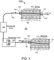
- Figure 1 is a schematic diagram of a tunable laser based on a reflective semiconductor optical amplifier (RSOA) combined with a semiconductor optical amplifier (SOA) according to an embodiment of the present invention. This diagram is merely an example, which should not unduly limit the scope of the claims.
- RSOA reflective semiconductor optical amplifier
- SOA semiconductor optical amplifier
- the tunable laser module 100 includes a RSOA with a first gain medium 110 on a silicon photonics substrate 10 to generate a stimulated emission, a wavelength tuner 170 formed in the silicon photonics substrate 10 and coupled to the RSOA to receive a reflected light in a wide band tuned based on the stimulated emission, a wavelength locker 180 formed in the silicon photonics substrate 10 and coupled to the wavelength tuner 170 to lock wavelengths of the light, and a SOA with a second gain medium 160 in an output path coupled to the wavelength locker to pass the light with a single amplification in power.
- the first gain medium 110 of RSOA is a laser chip flip-bonded on the silicon photonics substrate 10.
- the laser chip includes an active region 115 capped in a clad region configured in a waveguide form along its length throughout an optical cavity having a length L from a back facet 101 to a front facet 102, within which a stimulated emission or laser light is generated.
- the front facet 102 is characterized by a first reflectance Rf and the back facet 101 is characterized by a second reflectance Rb.
- the first reflectance Rf is very low in value, e.g., 0,005%, provided by an anti-reflective coating on the front facet 102.
- the second reflectance Rb is very high in value, e.g., >90%, provided by a high-reflective coating on the back facet 101.
- the active region 115 in waveguide form is configured to be in a curved shape with a non-perpendicular angle relative to the front facet 102 to reduce direct back reflection of the light thereby but with a substantially perpendicular angle relative to back facet 101 to maximize the reflection.
- the laser light is reflected by the back facet 101 and emitted out through the front facet 102 into a first waveguide 191 via a coupler 130. Through the first waveguide 191 the laser light is delivered to the wavelength tuner 170.
- the first gain medium 110 of RSOA is configured in a laser-diode chip to yield a high saturation power P sat at elevated temperature by design.
- the high saturation power means that the RSOA is configured to produce a high stable laser power.
- the higher saturation power can be achieved by using a low driving current with a shorter cavity to keep the gain high enough in order for it to operate at elevated temperature of -50 °C with a saturation power higher than 15dBm.
- the laser light after passing through the wavelength tuner 170 and wavelength locker 180, with its wavelength locked in a specific value in a wide-band spectrum (such as C-band), is inputted via an input coupler 150 in the SOA where it is further amplified in power before being outputted via an output coupler 140.
- the second gain medium 160 of SOA is another laser chip flip-bonded on the silicon photonics substrate 10.
- the gain medium 160 includes a gain region 165 capped in a clad region configured in a waveguide form extended in a length L through an amplifying cavity from a back facet 142 coupled to the input coupler 150 and a front facet 141 coupled to the output coupler 140.
- the front facet 141 is characterized by a first reflectance Rf and the back facet 142 is characterized by a second reflectance Rb.
- both the back facet 142 and the front facet 141 are coated by anti-reflective coating to give a very low value, e.g., 0.005%, of the first reflectance Rf and the second reflectance Rb for forming a symmetric semiconductor optical amplifier to allow the light to pass through once and be amplified in power.
- the active region 165 in waveguide form is configured to be in a curved shape with a non-perpendicular angle relative to either the back facet 142 or the front facet 141 to reduce direct back reflection of the light thereby.
- the second gain medium 160 of SOA can be also configured in a chip to yield a high saturation output power P sat >15dBm by design, meaning to have a high amplified maximum output power at elevated temperature of about 50 °C.
- d is a thickness of an active layer of the gain medium
- w is a width of the active layer
- ⁇ optical confinement factor
- a is a differential gain
- ⁇ s is carrier lifetime.
- Conventional methods have been used to improve P sat by increasing the width w of the active layer or reducing optical confinement factor ⁇ (or increasing ratio of d / ⁇ ) . Downside of reduced confinement factor or wider emitter is the gain is also reduced. In order to obtain higher gain for the device, longer cavity length and higher operating current are normally required to achieve high power. But high operating current mostly is not recommended for device in elevated temperature operation.
- the present disclosure provides an improved SOA (or RSOA) with high saturation power P sat for elevated temperature operation with reasonably high gain but reduced carrier lifetime ⁇ s and differential gain a by providing a gain medium with n-doped active layer in the gain chip for the SOA or RSOA.
- Figure 2 is a schematic diagram of a RSOA with a gain medium in both top and side views according to an embodiment of the present invention. This diagram is merely an example, which should not unduly limit the scope of the claims. One of ordinary skill in the art would recognize many variations, alternatives, and modifications.
- a top view of the gain medium 110 of the RSOA reveals a linear active region 115 laid in an optical cavity between a front facet with anti-reflective (AR) coating and a back facet with high-reflective (HR) coating.
- AR anti-reflective
- HR high-reflective
- a cross-section side view of the main medium 110 reveals a multi-layer structure with the active region 115 is shown as an active layer in a central portion of the multi-layer structure sandwiched between a P-layer at upper portion and a N-layer at lower portion which forms a semiconductor diode with a p-type electrode (p-metal) on the P-layer at the upper portion and a n-type electrode (n-metal) beneath the N-layer at the lower portion.
- the terms of upper or lower merely are referred to the figure illustration and do not limit actual device in just one setting in orientation.
- the P-layer includes a p-type optical confinement layer and a p-type clad layer.
- the N-layer includes a n-type optical confinement layer and a n-type clad layer.
- the N-layer is formed on a substrate and the n-metal is formed at a back side of the substrate.
- the semiconductor diode is configured as a laser diode with the optical cavity between the front facet and the back facet for RSOA.
- the active layer 115 When the laser diode is driven by a current source across the p-type electrode and the n-type electrode, a carrier-stimulated emission in the active layer 115 is generated between the front facet and the back facet before lasing out the front facet.
- the active layer 115 is provided as a n-doped layer to increase carrier density and reduces the carrier lifetime significantly.
- the active layer 115 itself is also a multilayer structure configured to form a multi-quantum-well structure.
- the n-type dopant for the active layer 115 can be Si or Se.
- the doping concentration can be in a range of 1.0 ⁇ 10 18 cm -3 to 3.0 ⁇ 10 18 cm -3 .
- P-doped active layer may be employed to reduce the carrier lifetime but it also causes high differential gain. Thus, p-doped active layer is not a good solution for improving Psat of RSOA by reducing differential gain.
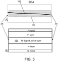
- FIG 3 is a schematic diagram of a SOA with a gain medium in both top and side views according to an embodiment of the present invention.
- This diagram is merely an example, which should not unduly limit the scope of the claims.
- the gain medium for SOA can be substantially same as the gain medium for RSOA described above in Figure 2 .
- a top view of the gain medium 160 of the SOA reveals a linear active region 165 laid in a cavity between a back facet and a front facet both with anti-reflective coating.
- a cross-section side view of the main medium 160 reveals a multi-layer structure with the active region 165 is shown as an active layer in a central portion of the multi-layer structure sandwiched between a P-layer at upper portion and a N-layer at lower portion which forms a semiconductor diode with a p-type electrode (p-metal) on the P-layer at the upper portion and a n-type electrode (n-metal) beneath the N-layer at the lower portion.
- the terms of upper or lower merely are referred to the figure illustration and do not limit actual device in just one setting in orientation.
- the P-layer includes a p-type optical confinement layer and a p-type clad layer.
- the N-layer includes a n-type optical confinement layer and a n-type clad layer.
- the N-layer is formed on a substrate and the n-metal is formed at a back side of the substrate.
- the semiconductor diode is configured as a laser diode with the optical cavity between the back facet and the front facet for SOA.
- the active layer 165 itself is a multilayer structure configured to form a multi-quantum-well structure or a hetero-junction structure.
- different semiconductor materials including one or more compound semiconductors or a combination of InAsP, GaInNAs, GaInAsP, GaInAs, and AlGaInAs may be employed for forming the multi-layers in the active layer with multi-quantum-well structure.
- the n-type dopant for the active layer 165 can be Si or Se.
- the doping concentration can be in a range of 1.0 ⁇ 10 18 cm -3 to 3.0 ⁇ 10 18 cm -3 .
- the active layer 165 is substantially the same as the active layer 115 in a multi-layer structure and in composition of respective layer within the multi-layer structure.
- both the active layer 165 and the active layer 115 are respective parts of two gain chips diced from a same die in a same wafer fabricated under a same semiconductor manufacture process.
- the active layer 115 of RSOA or the active layer 165 of SOA is a modulated n-doped multi-quantum-well structure.
- the multi-quantum-well structure of the active layer provides a hetero-junction structure including multiple well layers separated by respective barrier layers to achieve high-power light wave oscillation to yield high saturation lasing power for RSOA or output power for SOA comparing to a bulk active layer
- Figure 4 is a simplified bandgap diagram of a modulated n-doped active layer in the gain medium of RSOA/SOA according to an embodiment of the present invention. This diagram is merely an example, which should not unduly limit the scope of the claims.
- One of ordinary skill in the art would recognize many variations, alternatives, and modifications.
- the active layer provides a physical stack of multilayers including multiple well layers 11 separated by respective barrier layers 12.
- the active layer stack is located between an upper optical confinement stack and a lower optical confinement stack.
- the upper optical confinement stack is further attached with an upper clad layer and the lower optical confinement stack is further attached with a lower clad layer.
- the upper optical confinement stack plus the upper clad is provided as a P-layer with p-type doping characteristics as shown in Figure 2 and Figure 3 .
- the lower optical confinement stack plus the lower clad layer is provided as a N-layer with n-type doping characteristics as shown in Figure 2 and Figure 3 .
- the clad layer is selected from InP-based semiconductor material with different doping characteristics.
- the upper optical confinement stack includes a barrier layer 10a, two confinement layers 21a and 22a with different thicknesses and different bandgaps.
- the lower optical confinement stack in the example also includes a barrier layer 10b and two confinement layers 21b and 22b with different thicknesses and different bandgaps.
- the present invention provides a gain medium with modulated n-doped active layer stack for generating high saturation power in a semiconductor amplifier such as RSOA and SOA.
- a semiconductor amplifier such as RSOA and SOA.
- the specific material choices for the well layer and barrier layer, and parameters like thickness and doping characteristics are varied to yield different bandgaps and oscillation characteristics for the emitted light within the active layer stack in order to provide a specific light spectrum range that is fit, for example, for the application of the RSOA or SOA in forming a C-band or O-band wavelength tunable laser.
- the active layer stack is composed by three well layers 11 with a thickness t1 and a low energy bandgap of about 0.8eV which is in a corresponding amplified wavelength range.
- the SOA or RSOA is for amplifying wavelength in C-band.
- Each pair of well layers is separated by a barrier layer 12 with a thickness t2 and an energy bandgap of about 0.9-1.1eV.
- the well thickness is about 4-8 nm.
- the barrier thickness is about 5-15 nm.
- the well layer 11 is selected from an InGaP-based composite semiconductor material.
- the barrier layer 12 is selected from a GaInAs-based composite semiconductor material.
- the active layer stack is modulated n-doped such that the well layer 11 is undoped and the barrier layer 12 is doped by n-type impurity.
- the n-type doping area 15 in the barrier layer 12 includes a width no greater than that of the barrier layer thickness t2.
- the n-type doping area 15 contains Si (or Se) with a concentration in a range of 1.0 ⁇ 10 18 cm -3 to 3.0 ⁇ 10 18 cm -3 and a width in a range of 7 nm to 10 nm if the barrier layer is 10nm.
- a barrier layer 10a (10b) is provided between the confinement layer stack and the active layer stack.
- this barrier layer 10a (10b) also contains a n-doping area width, a doping concentration, and an energy bandgap all are comparable to or substantially the same as those characteristics in the barrier layer 12.
- the upper confinement stack includes a first p-type confinement sublayer 21a of a thickness of about 5-15 nm same as that of the barrier layer 10a, and a bandgap of about 0.9-1.1eV slightly higher than that of the barrier layer 10a (same as the active layer stack at about 0.9-1.1eV) to contain the charged carrier within the active layer stack.
- the upper confinement stack includes a second p-type confinement sublayer 22a of a thickness of about 15-25 nm and a bandgap of about 1.1-1.2eV higher than that of the first p-type confinement sublayer 21a to more effectively contain the charged carriers within the active layer stack for generating stimulated emission.
- the lower confinement stack includes a first n-type confinement sublayer 21b of a thickness of about 5-15 nm same as that of the barrier layer 10b, and a bandgap of about 0.9-1.1eV slightly higher than that of the barrier layer 10b (same as the active layer stack at about 1eV).
- the lower confinement stack also includes a second p-type confinement sublayer 22b of a thickness of about 38 nm and a bandgap of about 1.1-1.2eV.
- the upper clad has an even higher bandgap of about 1.3-1.4eV.
- the upper clad is InP doped with p-type dopant.
- the lower clad also has a bandgap of about 1.3-1.4eV and made by InP doped with n-type dopant.
- the gain of the gain medium containing the modulated n-doped active layer stack is kept high enough to have the RSOA or SOA device to operate at lower injected current with smaller cavity length so that the device can be operated at elevated temperature of 50 °C or higher.
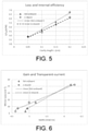
- Figure 5 is a graph showing the relation between the reciprocal of internal efficiency and cavity length of a gain medium with/without n-doped active layer in a nominal optical cavity according to an embodiment of the present invention.
- This diagram is merely an example, which should not unduly limit the scope of the claims.
- One of ordinary skill in the art would recognize many variations, alternatives, and modifications.
- the reciprocal of external differential quantum efficiency and is plotted against cavity length of a gain medium for either a conventional un-doped active layer stack ( ⁇ ) or a modulated n-doped active layer stack (O). These data are collected from cavity length varied from 0.05 cm to 0.2 cm.
- the solid line and the dashed line are respective linear fit lines for the two sets of data.
- the internal loss is calculated from the gradient of each straight line (solid or dashed). Hence, the modulated n-doped active layer yields a lower loss (see Table 1 below) compared to the case with the un-doped active layer In consequence, the internal losses of the gain medium without and with the n-doped active layer stack were estimated at 8.96 cm -1 and 6.77 cm -1 , respectively. This indicates that the internal efficiency can be improved for achieving higher output power by modulation doping with the n-type dopant in the active layer stack of the gain medium. Table I Wafer T (°C) Loss cm -1 ⁇ i (%) Go cm -1 J tr mA/cm Std 25 8.96 0.89 14.42 41.73 n-doped 25 6.77 0.84 11.12 27.21
- Figure 6 is a graph showing the relation between mirror loss and transparent current density of a gain medium in a nominal optical cavity according to an embodiment of the present invention.
- This diagram is merely an example, which should not unduly limit the scope of the claims.
- the gain medium as it is applied in a nominal optical cavity, also has a mirror loss depending on reflectance values of two facets thereof As shown, the mirror loss of the gain medium in a nominal optical cavity (with about 27% reflectivity) containing an undoped active layer stack ( ⁇ ) or a modulated n-doped active layer stack (O) is plotted against the logarithm of a threshold current density.
- the solid line and the dashed line are respective linear fit lines for the two sets of data.
- the threshold gain Go of the gain medium is calculated from the gradient of each straight line (solid or dashed), showing that Go is slightly lowered from 14.42 (cm -1 ) to 11.12 (cm -1 ) (see Table I above).
- a lower threshold gain value of the gain medium leads to a lower differential gain.
- lower differential gain results in higher saturation power of the gain medium can produce, which translates to a higher lasing power as the gain medium is in a RSOA device and a higher maximum output power as the gain medium is in a SOA device, and combined, a higher output power for the tunable laser based on the RSOA and SOA.
- a transparent current density J tr can be obtained as the current density at cavity length of infinity, or the mirror loss equals zero.
- the results of Table I indicate that the transparent current density J tr is lowered a lot at about 27 mA/cm 2 for the gain medium with n-doped active layer stack compared to about 42 mA/cm 2 for the gain medium with undoped active layer stack.
- Lower transparent current density means lower carrier lifetime, which yields higher saturation power as shown in the expression (1).
- the chip gain for either a RSOA or SOA device with the gain medium as described in a typical 1mm cavity length can be still at least 20dB (at room temperature) with a nominal operating current of about 300mA. This ensures a high saturation power of at least 15 dBm when the ROSA or SOA device is operated at elevated temperature of about 50 °C. There is no need to extend the cavity length or hike the injection current in order to achieve high enough gain especially at the elevated temperature environment. Additionally, the gain medium with the modulated n-doped active layer stack being applied in the RSOA device or SOA device has much higher mirror loss than typical laser device due to the facet reflectance setting of the gain medium cavity given a similar cavity length.
- a mirror loss is about 49.5 cm -1 .
- the mirror loss is about 90 cm -1 or greater.
Landscapes
- Physics & Mathematics (AREA)
- Condensed Matter Physics & Semiconductors (AREA)
- General Physics & Mathematics (AREA)
- Electromagnetism (AREA)
- Optics & Photonics (AREA)
- Semiconductor Lasers (AREA)
Abstract
Description
- The present invention relates to optical telecommunication techniques. More particularly, the present invention provides a semiconductor optical amplifier in silicon photonics platform for high-power elevated temperature operation.
- Over the last few decades, the use of communication networks exploded. In the early days Internet, popular applications were limited to emails, bulletin board, and mostly informational and text-based web page surfing, and the amount of data transferred was usually relatively small. Today, Internet and mobile applications demand a huge amount of bandwidth for transferring photo, video, music, and other multimedia files. For example, a social network like Facebook processes more than 500TB of data daily. With such high demands on data and data transfer, existing data communication systems need to be improved to address these needs.
- 40-Gbit/s and then 100-Gbit/s data rates wide-band DWDM (Dense Wavelength Division Multiplexed) optical transmission over existing single-mode fiber is a target for the next generation of fiber-optic communication networks. More recently, optical components are being integrated on silicon substrates for fabricating large-scale photonic integrated circuits that coexist with micro-electronic chips. a whole range of photonic components, including filters, (de)multiplexers, splitters, modulators, and photodetectors, have been demonstrated, mostly in the silicon-photonics platform. The silicon-photonics platform on silicon-on-insulator substrate is especially suited for standard WDM communication bands at 1300 nm and 1550 nm, as silicon (n = 3.48) and its oxide SiO2 (n = 1.44) are both transparent, and form high-index contrast, high-confinement waveguides ideally suited for medium to high-integration silicon photonics integrated circuits (SPICs).
- Semiconductor optical amplifier in silicon photonics platform have been implemented for many applications of optical telecommunication. For example, wavelength tunable laser based on the semiconductor optical amplifier is provided as key elements in SPICs for wide-band optical communication with increasing spectral efficiency. However, technical challenges exist for developing high-power semiconductor optical amplifier (SOA) or reflective semiconductor optical amplifier (RSOA) for elevated temperature operation in wide-band high-speed data communication application. Therefore, improved techniques are desired.
- The present invention relates to optical telecommunication techniques. One aspect of the present invention provides a reflective semiconductor optical amplifier (RSOA) and/or a semiconductor optical amplifier (SOA) for tunable lasers with high-power in elevated temperature operation. More particularly, the present invention provides a gain medium having a n-type doped active layer applied in RSOA/SOA to provide high saturation power at elevated temperature for making a wide-band wavelength tunable laser in high-speed data communication application, though other applications are possible.
- In an embodiment, the present invention provides a semiconductor optical amplifier for high-power operation. The semiconductor optical amplifier includes a gain medium including a multilayer structure sequentially laid with a P-layer, an active layer, a N-layer from an upper portion to a lower portion in cross-section thereof and extendedly laid with a length L from a front facet to a back facet thereof. The active layer comprises multiple well layers formed by undoped semiconductor material and multiple barrier layers formed by n-doped semiconductor materials. Each well layer is sandwiched by a pair of barrier layers. The front facet is characterized by a first reflectance Rf and the back facet is characterized by a second reflectance Rb. The gain medium has a mirror loss αm about 40-200 cm-1 given by: αm = (1/2L) ln{1/(Rf×Rb)}.
- Optionally, the gain medium is configured to produce a saturation power at least greater than 15 dBm with operation temperature up to 50 °C.
- Optionally, the active layer includes multiple barrier layers of a width about 5-15 nm with a bandgap of about 0.9-1.1eV.
- Optionally, each barrier layer includes a modulation doping area with n-type dopant concentration range of 1.0×1018 cm-3 to 3.0×1018 cm-3 in a width range of 7 nm to 10 nm.
- Optionally, the active layer includes multiple well layers of a width about 4-8 nm with a bandgap in a corresponding amplified wavelength range. For C-band, the bandgap is about 0.8eV.
- Optionally, the gain medium has a mirror loss greater than 45-100 cm-1 for the length L of 1 mm as the front facet is provided with an anti-reflective coating with the first reflectance Rf about 0.005% or smaller and the back facet is provided with a high-reflective coating with the second reflectance Rb greater than 90% for forming a reflective semiconductor optical amplifier.
- Optionally, the gain medium is configured as an optical cavity for amplifying a stimulated emission in the active layer, wherein the stimulated emission is reflected from the back facet and emitted out the front facet.
- Optionally, the active layer is made of a linear waveguide through the optical cavity, wherein the linear waveguide forms a non-perpendicular angle relative to the front facet and a substantially perpendicular angle relative to the back facet.
- Optionally, the gain medium has a mirror loss greater than 90-200 cm-1 for the length L of 1 mm as the front facet is provided with an anti-reflective coating with the first reflectance Rf about 0.005% or smaller and the back facet is provided with anti-reflective coating with the second reflectance Rb about 0.005% or smaller for forming a symmetric semiconductor optical amplifier.
- Optionally, the gain medium is configured as an optical cavity for amplifying a laser light in the active layer wherein the laser light is inputted through the back facet once and emitted out the front facet.
- Optionally, the active layer is made of a linear waveguide through the optical cavity, wherein the linear waveguide forms a non-perpendicular angle relative to the front facet and a non-perpendicular angle relative to the back facet.
- Optionally, the P-layer comprises a p-type confinement layer attached to an upper portion of the active layer and a p-type clad layer attached to a side of the p-type confinement layer more distal to the active layer.
- Optionally, the p-type confinement layer includes a first confinement sublayer of a 5-15nm thickness with a bandgap of about 0.9-1.1eV attached to a barrier layer with a slightly smaller bandgap of about 0.9-1.1eV next to the upper portion of the active layer and a second confinement sublayer of a 15-25nm thickness and a bandgap of about 1.1-1.2eV attached to a side of the first confinement sub-layer more distal to the active layer.
- Optionally, the N-layer comprises a n-type confinement layer attached to a lower portion of the active layer and a n-type clad layer attached to a side of the n-type confinement layer more distal to the active layer.
- Optionally, the n-type confinement layer comprises a first confinement sublayer of a 5-15nm thickness with a bandgap of about 0.9-1.1.eV attached to a barrier layer with a slightly smaller bandgap of about 0.9-1. 1eV next to the lower portion of the active layer and a second confinement sublayer of a 15-80nm thickness and a bandgap of about 1.1-1.2eV attached to a side of the first confinement sub-layer more distal to the active layer.
- In an alternative embodiment, the present invention provides wavelength-tunable laser in silicon photonics platform for high-power operation. The wavelength-tunable laser includes a silicon photonics substrate. Additionally, the wavelength-tunable laser includes a first semiconductor optical amplifier as described herein on the silicon photonics substrate. The gain medium is configured as an optical cavity with the front facet coated an anti-reflective coating and the back facet coated a high-reflective coating to produce a laser light amplified in the active layer thereof and reflected by the back facet before passing through the front facet. The wavelength-tunable laser further includes a wavelength tuner formed in the silicon photonics substrate and configured to receive the laser light via a first waveguide and tune wavelength of the laser light in a range of a wide-band. Furthermore, the wavelength-tunable laser includes a wavelength locker formed in the silicon photonics substrate and configured to couple with the wavelength tuner and lock the wavelength of the laser light and deliver the laser light via a second waveguide. Moreover, the wavelength-tunable laser includes a second semiconductor optical amplifier as described herein on the silicon photonics substrate. The gain medium is configured as an optical cavity with the front facet coated an anti-reflective coating and the back facet coated an anti-reflective coating, the laser light being inputted through the back facet and amplified in the active layer thereof before outputting through the front facet.
- Optionally, the active layer in the gain medium of the first semiconductor optical amplifier comprises multiple well layers formed by undoped semiconductor material in 6 nm thickness with a bandgap in a corresponding amplified wavelength range and multiple barrier layers formed by n-doped semiconductor materials in a doping concentration of 10×1018 cm-3 to 3.0×1018 cm-3 in a 5-15 nm thickness with a bandgap of 0.9-1.1eV. Each well layer is sandwiched by a pair of barrier layers.
- Optionally, the active layer in the gain medium of the second semiconductor optical amplifier comprises multiple well layers formed by undoped semiconductor material in a 4-8 nm thickness with a bandgap in a corresponding amplified wavelength range and multiple barrier layers formed by n-doped semiconductor materials in a doping concentration of 1.0×1018 cm-3 to 3.0×1018 cm-3 in a 5-15 nm thickness with a bandgap of 0.9-1.1eV, each well layer being sandwiched by a pair of barrier layers
- Optionally, the gain medium of the first semiconductor optical amplifier has a mirror loss of about 45-100 cm-1 for a length of 1 mm; the gain medium of the second semiconductor optical amplifier has a mirror loss of about 90-200 cm-1 for a length of 1 mm.
- Optionally, the gain medium of the first semiconductor optical amplifier is configured to produce a saturation laser power of at least 15dBm at an elevated operation temperature 50 °C and the gain medium of the second semiconductor optical amplifier is configured to produce a maximum light power of at least 15dBm at an elevated operation temperature 50 °C.
- The present invention achieves these benefits and others in the context of known technology of semiconductor optical amplifier, optionally provided with a gain medium including a modulated n-doped active layer between a PN junction in waveguide form extended in a length from a front facet and a back facet. However, a further understanding of the nature and advantages of the present invention may be realized by reference to the latter portions of the specification and attached drawings.
- The following diagrams are merely examples, which should not unduly limit the scope of the claims herein. One of ordinary skill in the art would recognize many other variations, modifications, and alternatives. It is also understood that the examples and embodiments described herein are for illustrative purposes only and that various modifications or changes in light thereof will be suggested to persons skilled in the art and are to be included within the spirit and purview of this process and scope of the appended claims.
-
Figure 1 is a schematic diagram of a tunable laser based on a reflective semiconductor optical amplifier (RSOA) combined with a semiconductor optical amplifier (SOA) according to an embodiment of the present invention. -
Figure 2 is a schematic diagram of a RSOA with a gain medium in both top and side views according to an embodiment of the present invention. -
Figure 3 is a schematic diagram of a SOA with a gain medium in both top and side views according to an embodiment of the present invention. -
Figure 4 is a simplified bandgap diagram of a modulated n-doped active layer in the gain medium of RSOA/SOA according to an embodiment of the present invention. -
Figure 5 is a graph showing the relation between the reciprocal of internal efficiency and cavity length of a gain medium with/without n-doped active layer in a nominal optical cavity according to an embodiment of the present invention. -
Figure 6 is a graph showing the relation between mirror loss and transparent current density of a gain medium with/without n-doped active layer in a nominal cavity according to an embodiment of the present invention. - The present invention relates to optical telecommunication techniques. One aspect of the present invention provides a reflective semiconductor optical amplifier (RSOA) and/or a semiconductor optical amplifier (SOA) with high-power gain medium for elevated-temperature operation. More particularly, the present invention provides RSOA/SOA with n doped active layer for making a wide-band wavelength-tunable laser in high-speed data communication application, though other applications are possible.
- The following description is presented to enable one of ordinary skill in the art to make and use the invention and to incorporate it in the context of particular applications. Various modifications, as well as a variety of uses in different applications will be readily apparent to those skilled in the art, and the general principles defined herein may be applied to a wide range of embodiments. Thus, the present invention is not intended to be limited to the embodiments presented, but is to be accorded the widest scope consistent with the principles and novel features disclosed herein.
- In the following detailed description, numerous specific details are set forth in order to provide a more thorough understanding of the present invention. However, it will be apparent to one skilled in the art that the present invention may be practiced without necessarily being limited to these specific details. In other instances, well-known structures and devices are shown in block diagram form, rather than in detail, in order to avoid obscuring the present invention.
- The reader's attention is directed to all papers and documents which are filed concurrently with this specification and which are open to public inspection with this specification, and the contents of all such papers and documents are incorporated herein by reference. All the features disclosed in this specification, (including any accompanying claims, abstract, and drawings) may be replaced by alternative features serving the same, equivalent or similar purpose, unless expressly stated otherwise. Thus, unless expressly stated otherwise, each feature disclosed is one example only of a generic series of equivalent or similar features.
- Furthermore, any element in a claim that does not explicitly state "means for" performing a specified function, or "step for" performing a specific function, is not to be interpreted as a "means" or "step" clause as specified in 35 U.S.C. Section 112, Paragraph 6. In particular, the use of "step of" or "act of" in the Claims herein is not intended to invoke the provisions of 35 U.S.C. 112, Paragraph 6.
- Please note, if used, the labels inner, outer, left, right, front, back, top, bottom, end, forward, reverse, clockwise and counter clockwise have been used for convenience purposes only and are not intended to imply any particular fixed direction. Instead, they are used to reflect relative locations and/or directions between various portions of an object.
- In an aspect, the present disclosure provides a reflective semiconductor optical amplifier (RSOA) and/or a semiconductor optical amplifier (SOA) with high-power operability at elevated temperature. In an example, the RSOA/SOA with high-power operability is applied to form a wide-band wavelength tunable laser in silicon photonics platform.
Figure 1 is a schematic diagram of a tunable laser based on a reflective semiconductor optical amplifier (RSOA) combined with a semiconductor optical amplifier (SOA) according to an embodiment of the present invention. This diagram is merely an example, which should not unduly limit the scope of the claims. One of ordinary skill in the art would recognize many variations, alternatives, and modifications. As shown, thetunable laser module 100 includes a RSOA with afirst gain medium 110 on asilicon photonics substrate 10 to generate a stimulated emission, awavelength tuner 170 formed in thesilicon photonics substrate 10 and coupled to the RSOA to receive a reflected light in a wide band tuned based on the stimulated emission, awavelength locker 180 formed in thesilicon photonics substrate 10 and coupled to thewavelength tuner 170 to lock wavelengths of the light, and a SOA with asecond gain medium 160 in an output path coupled to the wavelength locker to pass the light with a single amplification in power. - Optionally, the
first gain medium 110 of RSOA is a laser chip flip-bonded on thesilicon photonics substrate 10. The laser chip includes anactive region 115 capped in a clad region configured in a waveguide form along its length throughout an optical cavity having a length L from aback facet 101 to afront facet 102, within which a stimulated emission or laser light is generated. Thefront facet 102 is characterized by a first reflectance Rf and theback facet 101 is characterized by a second reflectance Rb. Optionally, the first reflectance Rf is very low in value, e.g., 0,005%, provided by an anti-reflective coating on thefront facet 102. Optionally, the second reflectance Rb is very high in value, e.g., >90%, provided by a high-reflective coating on theback facet 101. Optionally, theactive region 115 in waveguide form is configured to be in a curved shape with a non-perpendicular angle relative to thefront facet 102 to reduce direct back reflection of the light thereby but with a substantially perpendicular angle relative to backfacet 101 to maximize the reflection. The laser light is reflected by theback facet 101 and emitted out through thefront facet 102 into afirst waveguide 191 via acoupler 130. Through thefirst waveguide 191 the laser light is delivered to thewavelength tuner 170. In an embodiment for the tunable laser in high-power operation, thefirst gain medium 110 of RSOA is configured in a laser-diode chip to yield a high saturation power Psat at elevated temperature by design. The high saturation power means that the RSOA is configured to produce a high stable laser power. Yet, the higher saturation power can be achieved by using a low driving current with a shorter cavity to keep the gain high enough in order for it to operate at elevated temperature of -50 °C with a saturation power higher than 15dBm. - Referring to
Figure 1 , the laser light, after passing through thewavelength tuner 170 andwavelength locker 180, with its wavelength locked in a specific value in a wide-band spectrum (such as C-band), is inputted via aninput coupler 150 in the SOA where it is further amplified in power before being outputted via anoutput coupler 140. Optionally, thesecond gain medium 160 of SOA is another laser chip flip-bonded on thesilicon photonics substrate 10. Thegain medium 160 includes again region 165 capped in a clad region configured in a waveguide form extended in a length L through an amplifying cavity from aback facet 142 coupled to theinput coupler 150 and afront facet 141 coupled to theoutput coupler 140. In the embodiment, thefront facet 141 is characterized by a first reflectance Rf and theback facet 142 is characterized by a second reflectance Rb. Optionally, both theback facet 142 and thefront facet 141 are coated by anti-reflective coating to give a very low value, e.g., 0.005%, of the first reflectance Rf and the second reflectance Rb for forming a symmetric semiconductor optical amplifier to allow the light to pass through once and be amplified in power. Optionally, theactive region 165 in waveguide form is configured to be in a curved shape with a non-perpendicular angle relative to either theback facet 142 or thefront facet 141 to reduce direct back reflection of the light thereby. This light received via theback facet 142 from theinput coupler 150 is simply passed through the length L of the cavity and amplified therein before outputting via thefront facet 141. In the embodiment, for making the tunable laser in high-power operation, thesecond gain medium 160 of SOA can be also configured in a chip to yield a high saturation output power Psat >15dBm by design, meaning to have a high amplified maximum output power at elevated temperature of about 50 °C. - In theory, the saturation output power Psat of a gain medium or a laser-diode chip can be expressed as following:

- The present disclosure provides an improved SOA (or RSOA) with high saturation power Psat for elevated temperature operation with reasonably high gain but reduced carrier lifetime τs and differential gain a by providing a gain medium with n-doped active layer in the gain chip for the SOA or RSOA.
Figure 2 is a schematic diagram of a RSOA with a gain medium in both top and side views according to an embodiment of the present invention. This diagram is merely an example, which should not unduly limit the scope of the claims. One of ordinary skill in the art would recognize many variations, alternatives, and modifications. As shown in part A), a top view of thegain medium 110 of the RSOA reveals a linearactive region 115 laid in an optical cavity between a front facet with anti-reflective (AR) coating and a back facet with high-reflective (HR) coating. In part B) ofFigure 2 , a cross-section side view of themain medium 110 reveals a multi-layer structure with theactive region 115 is shown as an active layer in a central portion of the multi-layer structure sandwiched between a P-layer at upper portion and a N-layer at lower portion which forms a semiconductor diode with a p-type electrode (p-metal) on the P-layer at the upper portion and a n-type electrode (n-metal) beneath the N-layer at the lower portion. Note, the terms of upper or lower merely are referred to the figure illustration and do not limit actual device in just one setting in orientation. Optionally, the P-layer includes a p-type optical confinement layer and a p-type clad layer. Optionally, there is a contact layer between the P-layer and the p-metal. Optionally, the N-layer includes a n-type optical confinement layer and a n-type clad layer. Optionally, the N-layer is formed on a substrate and the n-metal is formed at a back side of the substrate. Optionally, the semiconductor diode is configured as a laser diode with the optical cavity between the front facet and the back facet for RSOA. - When the laser diode is driven by a current source across the p-type electrode and the n-type electrode, a carrier-stimulated emission in the
active layer 115 is generated between the front facet and the back facet before lasing out the front facet. Optionally, theactive layer 115 is provided as a n-doped layer to increase carrier density and reduces the carrier lifetime significantly. Optionally, theactive layer 115 itself is also a multilayer structure configured to form a multi-quantum-well structure. Depending on working wavelength spectrum, different semiconductor materials including one or more compound semiconductors or a combination of InAsP, GaInNAs, GaInAsP, GaInAs, and AlGaInAs may be employed for forming the multi-layers in the active layer with multi-quantum-well structure. Optionally, the n-type dopant for theactive layer 115 can be Si or Se. Optionally, the doping concentration can be in a range of 1.0×1018 cm-3 to 3.0×1018 cm-3. - Although P-doped active layer may be employed to reduce the carrier lifetime but it also causes high differential gain. Thus, p-doped active layer is not a good solution for improving Psat of RSOA by reducing differential gain.
-
Figure 3 is a schematic diagram of a SOA with a gain medium in both top and side views according to an embodiment of the present invention. This diagram is merely an example, which should not unduly limit the scope of the claims. One of ordinary skill in the art would recognize many variations, alternatives, and modifications. In an embodiment, the gain medium for SOA can be substantially same as the gain medium for RSOA described above inFigure 2 . Similarly, in Part A), a top view of thegain medium 160 of the SOA reveals a linearactive region 165 laid in a cavity between a back facet and a front facet both with anti-reflective coating. In part B) ofFigure 3 , a cross-section side view of themain medium 160 reveals a multi-layer structure with theactive region 165 is shown as an active layer in a central portion of the multi-layer structure sandwiched between a P-layer at upper portion and a N-layer at lower portion which forms a semiconductor diode with a p-type electrode (p-metal) on the P-layer at the upper portion and a n-type electrode (n-metal) beneath the N-layer at the lower portion. Note, the terms of upper or lower merely are referred to the figure illustration and do not limit actual device in just one setting in orientation. Optionally, the P-layer includes a p-type optical confinement layer and a p-type clad layer. Optionally, there is a contact layer between the P-layer and the p-metal. Optionally, the N-layer includes a n-type optical confinement layer and a n-type clad layer. Optionally, the N-layer is formed on a substrate and the n-metal is formed at a back side of the substrate. Optionally, the semiconductor diode is configured as a laser diode with the optical cavity between the back facet and the front facet for SOA. - Optionally, the
active layer 165 itself is a multilayer structure configured to form a multi-quantum-well structure or a hetero-junction structure. Depending on working wavelength spectrum, different semiconductor materials including one or more compound semiconductors or a combination of InAsP, GaInNAs, GaInAsP, GaInAs, and AlGaInAs may be employed for forming the multi-layers in the active layer with multi-quantum-well structure. Optionally, the n-type dopant for theactive layer 165 can be Si or Se. Optionally, the doping concentration can be in a range of 1.0×1018 cm-3 to 3.0×1018 cm-3. Optionally, theactive layer 165 is substantially the same as theactive layer 115 in a multi-layer structure and in composition of respective layer within the multi-layer structure. Optionally, both theactive layer 165 and theactive layer 115 are respective parts of two gain chips diced from a same die in a same wafer fabricated under a same semiconductor manufacture process. - In an embodiment, the
active layer 115 of RSOA or theactive layer 165 of SOA is a modulated n-doped multi-quantum-well structure. The multi-quantum-well structure of the active layer provides a hetero-junction structure including multiple well layers separated by respective barrier layers to achieve high-power light wave oscillation to yield high saturation lasing power for RSOA or output power for SOA comparing to a bulk active layerFigure 4 is a simplified bandgap diagram of a modulated n-doped active layer in the gain medium of RSOA/SOA according to an embodiment of the present invention. This diagram is merely an example, which should not unduly limit the scope of the claims. One of ordinary skill in the art would recognize many variations, alternatives, and modifications. As shown, the active layer provides a physical stack of multilayers including multiple well layers 11 separated by respective barrier layers 12. The active layer stack is located between an upper optical confinement stack and a lower optical confinement stack. The upper optical confinement stack is further attached with an upper clad layer and the lower optical confinement stack is further attached with a lower clad layer. Optionally, the upper optical confinement stack plus the upper clad is provided as a P-layer with p-type doping characteristics as shown inFigure 2 andFigure 3 . Optionally, the lower optical confinement stack plus the lower clad layer is provided as a N-layer with n-type doping characteristics as shown inFigure 2 andFigure 3 . Optionally, the clad layer is selected from InP-based semiconductor material with different doping characteristics. Referring to an example shown inFigure 4 , the upper optical confinement stack includes abarrier layer 10a, twoconfinement layers barrier layer 10b and twoconfinement layers - In an aspect, the present invention provides a gain medium with modulated n-doped active layer stack for generating high saturation power in a semiconductor amplifier such as RSOA and SOA. The specific material choices for the well layer and barrier layer, and parameters like thickness and doping characteristics are varied to yield different bandgaps and oscillation characteristics for the emitted light within the active layer stack in order to provide a specific light spectrum range that is fit, for example, for the application of the RSOA or SOA in forming a C-band or O-band wavelength tunable laser.
- Referring to an embodiment shown in
Figure 4 , the active layer stack is composed by threewell layers 11 with a thickness t1 and a low energy bandgap of about 0.8eV which is in a corresponding amplified wavelength range. For example, the SOA or RSOA is for amplifying wavelength in C-band. Each pair of well layers is separated by abarrier layer 12 with a thickness t2 and an energy bandgap of about 0.9-1.1eV. Optionally, there can be two well layers. Optionally, there can be four well layers. Optionally, the well thickness is about 4-8 nm. Optionally, the barrier thickness is about 5-15 nm. Optionally, thewell layer 11 is selected from an InGaP-based composite semiconductor material. Optionally, thebarrier layer 12 is selected from a GaInAs-based composite semiconductor material. Optionally, the active layer stack is modulated n-doped such that thewell layer 11 is undoped and thebarrier layer 12 is doped by n-type impurity. Optionally, the n-type doping area 15 in thebarrier layer 12 includes a width no greater than that of the barrier layer thickness t2. Optionally, the n-type doping area 15 contains Si (or Se) with a concentration in a range of 1.0×1018 cm-3 to 3.0×1018 cm-3 and a width in a range of 7 nm to 10 nm if the barrier layer is 10nm. - Referring to
Figure 4 , optionally, abarrier layer 10a (10b) is provided between the confinement layer stack and the active layer stack. Optionally, thisbarrier layer 10a (10b) also contains a n-doping area width, a doping concentration, and an energy bandgap all are comparable to or substantially the same as those characteristics in thebarrier layer 12. Optionally, the upper confinement stack includes a first p-type confinement sublayer 21a of a thickness of about 5-15 nm same as that of thebarrier layer 10a, and a bandgap of about 0.9-1.1eV slightly higher than that of thebarrier layer 10a (same as the active layer stack at about 0.9-1.1eV) to contain the charged carrier within the active layer stack. the upper confinement stack includes a second p-type confinement sublayer 22a of a thickness of about 15-25 nm and a bandgap of about 1.1-1.2eV higher than that of the first p-type confinement sublayer 21a to more effectively contain the charged carriers within the active layer stack for generating stimulated emission. Similarly, the lower confinement stack includes a first n-type confinement sublayer 21b of a thickness of about 5-15 nm same as that of thebarrier layer 10b, and a bandgap of about 0.9-1.1eV slightly higher than that of thebarrier layer 10b (same as the active layer stack at about 1eV). Further, the lower confinement stack also includes a second p-type confinement sublayer 22b of a thickness of about 38 nm and a bandgap of about 1.1-1.2eV. Referring toFigure 4 , the upper clad has an even higher bandgap of about 1.3-1.4eV. Optionally, the upper clad is InP doped with p-type dopant. The lower clad also has a bandgap of about 1.3-1.4eV and made by InP doped with n-type dopant. - In the embodiment to implement the modulated n-doped active layer stack in the gain medium for RSOA or SOA to reduce carrier lifetime without increasing differential gain for achieving higher saturation power [see expression (1)]. At the same time, the gain of the gain medium containing the modulated n-doped active layer stack is kept high enough to have the RSOA or SOA device to operate at lower injected current with smaller cavity length so that the device can be operated at elevated temperature of 50 °C or higher.
-
Figure 5 is a graph showing the relation between the reciprocal of internal efficiency and cavity length of a gain medium with/without n-doped active layer in a nominal optical cavity according to an embodiment of the present invention. This diagram is merely an example, which should not unduly limit the scope of the claims. One of ordinary skill in the art would recognize many variations, alternatives, and modifications. As shown, the reciprocal of external differential quantum efficiency and is plotted against cavity length of a gain medium for either a conventional un-doped active layer stack (Δ) or a modulated n-doped active layer stack (O). These data are collected from cavity length varied from 0.05 cm to 0.2 cm. The solid line and the dashed line are respective linear fit lines for the two sets of data. The internal loss is calculated from the gradient of each straight line (solid or dashed). Apparently, the modulated n-doped active layer yields a lower loss (see Table 1 below) compared to the case with the un-doped active layer In consequence, the internal losses of the gain medium without and with the n-doped active layer stack were estimated at 8.96 cm-1 and 6.77 cm-1, respectively. This indicates that the internal efficiency can be improved for achieving higher output power by modulation doping with the n-type dopant in the active layer stack of the gain medium.Table I Wafer T (°C) Loss cm-1 ηi (%) Go cm-1 Jtr mA/ cm Std 25 8.96 0.89 14.42 41.73 n-doped 25 6.77 0.84 11.12 27.21 -
Figure 6 is a graph showing the relation between mirror loss and transparent current density of a gain medium in a nominal optical cavity according to an embodiment of the present invention. This diagram is merely an example, which should not unduly limit the scope of the claims. One of ordinary skill in the art would recognize many variations, alternatives, and modifications. In additional to the internal loss, the gain medium, as it is applied in a nominal optical cavity, also has a mirror loss depending on reflectance values of two facets thereof As shown, the mirror loss of the gain medium in a nominal optical cavity (with about 27% reflectivity) containing an undoped active layer stack (Δ) or a modulated n-doped active layer stack (O) is plotted against the logarithm of a threshold current density. The solid line and the dashed line are respective linear fit lines for the two sets of data. The threshold gain Go of the gain medium is calculated from the gradient of each straight line (solid or dashed), showing that Go is slightly lowered from 14.42 (cm-1) to 11.12 (cm-1) (see Table I above). A lower threshold gain value of the gain medium leads to a lower differential gain. Based on expression (1), lower differential gain results in higher saturation power of the gain medium can produce, which translates to a higher lasing power as the gain medium is in a RSOA device and a higher maximum output power as the gain medium is in a SOA device, and combined, a higher output power for the tunable laser based on the RSOA and SOA. Based on the graph ofFigure 6 , a transparent current density Jtr can be obtained as the current density at cavity length of infinity, or the mirror loss equals zero. The results of Table I indicate that the transparent current density Jtr is lowered a lot at about 27 mA/cm2 for the gain medium with n-doped active layer stack compared to about 42 mA/cm2 for the gain medium with undoped active layer stack. Lower transparent current density means lower carrier lifetime, which yields higher saturation power as shown in the expression (1). - Yet, for a slightly lower Go around 11 cm-1, the chip gain for either a RSOA or SOA device with the gain medium as described in a typical 1mm cavity length can be still at least 20dB (at room temperature) with a nominal operating current of about 300mA. This ensures a high saturation power of at least 15 dBm when the ROSA or SOA device is operated at elevated temperature of about 50 °C. There is no need to extend the cavity length or hike the injection current in order to achieve high enough gain especially at the elevated temperature environment. Additionally, the gain medium with the modulated n-doped active layer stack being applied in the RSOA device or SOA device has much higher mirror loss than typical laser device due to the facet reflectance setting of the gain medium cavity given a similar cavity length. For a RSOA device with a gain medium in a 1mm long cavity having one HR facet with >90% in reflectance and one AR facet with about 0.005% in reflectance, a mirror loss is about 49.5 cm-1. For a SOA device with a gain medium in a 1mm long cavity having both AR facets, the mirror loss is about 90 cm-1 or greater.
- While the above is a full description of the specific embodiments, various modifications, alternative constructions and equivalents may be used. Therefore, the above description and illustrations should not be taken as limiting the scope of the present invention which is defined by the appended claims.
- The following is a list of further preferred embodiments of the invention:
- Embodiment 1: A semiconductor optical amplifier for high-power operation comprising:
- a gain medium comprising a multilayer structure sequentially laid with a P-layer, an active layer, a N-layer from an upper portion to a lower portion in cross-section thereof and extendedly laid with a length L from a front facet to a back facet thereof, wherein
- the active layer comprises multiple well layers formed by undoped semiconductor material and multiple barrier layers formed by n-doped semiconductor materials; each well layer being sandwiched by a pair of barrier layers;
- the front facet is characterized by a first reflectance Rf and the back facet is characterized by a second reflectance Rb; and
- the gain medium has a mirror loss □m about 40 - 200 cm-1 given by:

- Embodiment 2: The semiconductor optical amplifier of embodiment 1 wherein the gain medium is configured to produce a saturation power at least greater than 15 dBm with operation temperature up to 50 °C.
- Embodiment 3: The semiconductor optical amplifier of embodiment 1 wherein the active layer comprises multiple barrier layers of a width about 5-15 nm with a bandgap of about 0.9-1.1eV.
- Embodiment 4: The semiconductor optical amplifier of embodiment 3 wherein each barrier layer comprises a modulation doping area with n-type dopant concentration range of 1.0×1018 cm-3 to 3.0×1018 cm-3 in a width range of 7 nm to 10 nm based on a barrier layer width of 10nm.
- Embodiment 5: The semiconductor optical amplifier of embodiment 1 wherein the active layer comprises multiple well layers of a width about 4-8 nm with a bandgap of about 0.8eV.
- Embodiment 6: The semiconductor optical amplifier of embodiment 1 wherein the gain medium has a mirror loss greater than 45-100 cm-1 for the length L of 1 mm as the front facet is provided with an anti-reflective coating with the first reflectance Rf about 0.005% or smaller and the back facet is provided with a high-reflective coating with the second reflectance Rb greater than 90% for forming a reflective semiconductor optical amplifier.
- Embodiment 7: The semiconductor optical amplifier of embodiment 6 wherein the gain medium is configured as an optical cavity for amplifying a stimulated emission in the active layer, wherein the stimulated emission is reflected from the back facet and emitted out the front facet.
- Embodiment 8: The semiconductor optical amplifier of embodiment 7 wherein the active layer is made of a linear waveguide through the optical cavity, wherein the linear waveguide forms a non-perpendicular angle relative to the front facet and a substantially perpendicular angle relative the back facet.
- Embodiment 9: The semiconductor optical amplifier of embodiment 1 wherein the gain medium has a mirror loss greater than 90-200 cm-1 for the length L of 1 mm as the front facet is provided with an anti-reflective coating with the first reflectance Rf about 0.005% or smaller and the back facet is provided with anti-reflective coating with the second reflectance Rb about 0.005% or smaller for forming a symmetric semiconductor optical amplifier.
- Embodiment 10: The semiconductor optical amplifier of embodiment 9 wherein the gain medium is configured as an optical cavity for amplifying a laser light in the active layer wherein the laser light is inputted through the back facet once and emitted out the front facet.
- Embodiment 11: The semiconductor optical amplifier of
embodiment 10 wherein the active layer is made of a linear waveguide through the optical cavity, wherein the linear waveguide forms a non-perpendicular angle relative to the front facet and a non-perpendicular angle relative to the back facet. - Embodiment 12: The semiconductor optical amplifier of embodiment 1 wherein the P-layer comprises a p-type confinement layer attached to an upper portion of the active layer and a p-type clad layer attached to a side of the p-type confinement layer more distal to the active layer.
- Embodiment 13: The semiconductor optical amplifier of
embodiment 12 wherein the p-type confinement layer comprises a first confinement sublayer of a 5-15 nm thickness with a bandgap of about 0.9 to 1.1eV attached to a barrier layer with a slightly smaller bandgap of about 0.9-1.1eV next to the upper portion of the active layer and a second confinement sublayer of a 15-25nm thickness and a bandgap of about 1.1-1.2eV attached to a side of the first confinement sub-layer more distal to the active layer. - Embodiment 14: The semiconductor optical amplifier of embodiment 1 wherein the N-layer comprises a n-type confinement layer attached to a lower portion of the active layer and a n-type clad layer attached to a side of the n-type confinement layer more distal to the active layer.
- Embodiment 15: The semiconductor optical amplifier of embodiment 14 wherein the n-type confinement layer comprises a first confinement sublayer of a 5-15nm thickness with a bandgap of about 0.9-1.1eV attached to a barrier layer with a slightly smaller bandgap of about 0.9-1.1eV next to the lower portion of the active layer and a second confinement sublayer of a 15-80nm thickness and a bandgap of about 1.1-1.2eV attached to a side of the first confinement sub-layer more distal to the active layer.
- Embodiment 16: A wavelength-tunable laser in silicon photonics platform for high-power operation comprising:
- a silicon photonics substrate;
- a first semiconductor optical amplifier of embodiment 1 on the silicon photonics substrate, wherein the gain medium is configured as a optical cavity with the front facet coated an anti-reflective coating and the back facet coated a high-reflective coating to produce a laser light amplified in the active layer thereof and reflected by the back facet before passing through the front facet;
- a wavelength tuner formed in the silicon photonics substrate and configured to receive the laser light via a first waveguide and tune wavelength of the laser light in a range of a wide-band;
- a wavelength locker formed in the silicon photonics substrate and configured to couple with the wavelength tuner and lock the wavelength of the laser light and deliver the laser light via a second waveguide; and
- a second semiconductor optical amplifier of embodiment 1 on the silicon photonics substrate, wherein the gain medium is configured as a optical cavity with the front facet coated an anti-reflective coating and the back facet coated an anti-reflective coating, the laser light being inputted through the back facet and amplified in the active layer thereof before outputting through the front facet.
- Embodiment 17: The wavelength-tunable lase of embodiment 16 wherein the active layer in the gain medium of the first semiconductor optical amplifier comprises multiple well layers formed by undoped semiconductor material in 4-8 nm thickness with a bandgap in corresponding amplified wavelength range and multiple barrier layers formed by n-doped semiconductor materials in a doping concentration of 1.0×1018 cm-3 to 3.0×1018 cm-3 in a 5-15 nm thickness with a bandgap of 1.0eV; each well layer being sandwiched by a pair of barrier layers.
- Embodiment 18: The wavelength-tunable lase of embodiment 16 wherein the active layer in the gain medium of the second semiconductor optical amplifier comprises multiple well layers formed by undoped semiconductor material in a 4-8 nm thickness with a bandgap in corresponding amplified wavelength range and multiple barrier layers formed by n-doped semiconductor materials in a doping concentration of 1.0×1018 cm-3 to 3.0×1018 cm-3 in a 5-15 nm thickness with a bandgap of 0.9-1.1eV; each well layer being sandwiched by a pair of barrier layers.
- Embodiment 19: The wavelength-tunable lase of embodiment 16 wherein the gain medium of the first semiconductor optical amplifier has a mirror loss of about 45-100 cm-1 for a length of 1 mm; the gain medium of the second semiconductor optical amplifier has a mirror loss of about 90-200 cm-1 for a length of 1 mm.
- Embodiment 20: The wavelength-tunable lase of embodiment 16 wherein the gain medium of the first semiconductor optical amplifier is configured to produce a saturation laser power of at least 15dBm at an elevated operation temperature 50 °C and the gain medium of the second semiconductor optical amplifier is configured to produce a maximum light power of at least 15dBm at an elevated operation temperature 50 °C.
Claims (15)
- A semiconductor optical amplifier for high-power operation of a tunable laser (100), the semiconductor optical amplifier comprising:a gain medium (110, 160) comprising a multilayer structure with a P-layer and an N-layer;a front facet (102, 141) having a first reflectance; anda back facet (101, 142) having a second reflectance,characterized in that:the first reflectance and the second reflectance are configured such that the gain medium at least one of generates, reflects, and amplifies laser light; andan N-doped active layer (115, 165) having undoped well layers (11) alternating with N-doped barrier layers (15) is formed between the P-layer and the N-layer.
- The semiconductor optical amplifier of claim 1, wherein:the gain medium has a length L from the front facet to the back facet; andthe gain medium has a mirror loss □m between 40 and 200 cm-1 in accordance with □m =(1/2L)In{1/(Rf×Rb)}, where Rf is the first reflectance and Rb is the second reflectance.
- The semiconductor optical amplifier of claim 1, wherein the N-doped active layer is configured to provide saturation power of at least 15 dBm with an operation temperature up to 50 °C for the gain medium.
- The semiconductor optical amplifier of claim 1, wherein the N-doped barrier layers have a width between 5 and 15 nm and a bandgap between 0.9 and 1.1 eV.
- The semiconductor optical amplifier of claim 4, wherein each of the N-doped barrier layers comprises a modulation doping area (15) with an N-type dopant concentration range of 1.0×1018 cm-3 to 3.0×1018 cm-3 in a width range of 7 nm to 10 nm based on a barrier layer width of 10 nm.
- The semiconductor optical amplifier of claim 1, wherein the undoped well layers have a width between 4 and 8 nm and a bandgap of 0.8 eV.
- The semiconductor optical amplifier of claim 1, wherein the gain medium has a mirror loss greater than 45-100 cm-1 for a length of 1 mm, the front facet is provided with an anti-reflective coating, the first reflectance is less than or equal to 0.005%, the back facet is provided with a reflective coating, and the second reflectance is greater than 90%.
- The semiconductor optical amplifier of claim 7, wherein the N-doped active layer is configured as a linear waveguide through an optical cavity of the gain medium, and wherein the linear waveguide forms a non-perpendicular angle relative to the front facet and a substantially perpendicular angle relative to the back facet.
- The semiconductor optical amplifier of claim 1, wherein the gain medium has a mirror loss greater than 90-200 cm-1 for a length of 1 mm, the front facet is provided with an anti-reflective coating, the first reflectance is less than or equal to 0.005%, the back facet is provided with an anti-reflective coating, and the second reflectance is less than or equal to 0.005% to form a symmetric semiconductor optical amplifier.
- The semiconductor optical amplifier of claim 9, wherein the gain medium is configured as an optical cavity for amplifying the laser light in the N-doped active layer, and wherein the laser light is input through the back facet once and emitted through the front facet.
- The semiconductor optical amplifier of claim 10, wherein the N-doped active layer is configured as a linear waveguide through an optical cavity of the gain medium, and wherein the linear waveguide forms a non-perpendicular angle relative to the front facet and a non-perpendicular angle relative to the back facet.
- The semiconductor optical amplifier of claim 1, wherein the P-layer comprises a P-type confinement layer attached to an upper portion of the N-doped active layer and a P-type clad layer attached to a side of the P-type confinement layer more distal to the N-doped active layer than the P-type confinement layer.
- The semiconductor optical amplifier of claim 12, wherein the P-type confinement layer comprises (i) a first confinement sublayer (21a) having a thickness between 5 and 15 nm with a bandgap between 0.9 and 1.1 eV attached to a barrier layer (10a) with a bandgap between 0.9 and 1.1 eV next to the upper portion of the active layer and (ii) a second confinement sublayer (22a) having a thickness between 15 and 25 nm and a bandgap between 1.1 and 1.2 eV attached to a side of the first confinement sublayer more distal to the N-doped active layer than the first confinement sublayer.
- The semiconductor optical amplifier of claim 1, wherein the N-layer comprises an N-type confinement layer attached to a lower portion of the N-doped active layer and an N-type clad layer attached to a side of the N-type confinement layer more distal to the N-doped active layer than the N-type confinement layer.
- The semiconductor optical amplifier of claim 14, wherein the N-type confinement layer comprises (i) a first confinement sublayer (21b) having a thickness between 5 and 15 nm with a bandgap between 0.9 and 1.1 eV attached to a barrier layer (10b) with a bandgap between 0.9 and 1.1 eV next to the lower portion of the N-doped active layer and (ii) a second confinement sublayer (22b) having a thickness between 15 and 80 nm and a bandgap between 1.1 and 1.2 eV attached to a side of the first confinement sublayer more distal to the N-doped active layer than the first confinement sublayer.
Applications Claiming Priority (1)
| Application Number | Priority Date | Filing Date | Title |
|---|---|---|---|
| US17/024,473 US11929592B2 (en) | 2020-09-17 | 2020-09-17 | Silicon-photonics-based semiconductor optical amplifier with N-doped active layer |
Publications (1)
| Publication Number | Publication Date |
|---|---|
| EP3972063A1 true EP3972063A1 (en) | 2022-03-23 |
Family
ID=77821658
Family Applications (1)
| Application Number | Title | Priority Date | Filing Date |
|---|---|---|---|
| EP21197432.4A Pending EP3972063A1 (en) | 2020-09-17 | 2021-09-17 | Silicon-photonics-based semiconductor optical amplifier with n-doped active layer |
Country Status (3)
| Country | Link |
|---|---|
| US (1) | US11929592B2 (en) |
| EP (1) | EP3972063A1 (en) |
| CN (1) | CN114284863A (en) |
Families Citing this family (1)
| Publication number | Priority date | Publication date | Assignee | Title |
|---|---|---|---|---|
| US20240372325A1 (en) * | 2021-03-31 | 2024-11-07 | Sumitomo Electric Device Innovations, Inc. | Variable-wavelength laser |
Citations (2)
| Publication number | Priority date | Publication date | Assignee | Title |
|---|---|---|---|---|
| US20120099185A1 (en) * | 2010-10-26 | 2012-04-26 | Tohoku University | Laser diode assembly and semiconductor optical amplifier assembly |
| US20170040775A1 (en) * | 2014-04-21 | 2017-02-09 | Fujitsu Limited | Tunable laser source, optical transmitter, and optical transmitter and receiver module |
Family Cites Families (66)
| Publication number | Priority date | Publication date | Assignee | Title |
|---|---|---|---|---|
| US4163238A (en) * | 1978-06-09 | 1979-07-31 | The United States Of America As Represented By The Secretary Of The Army | Infrared semiconductor device with superlattice region |
| US4881235A (en) * | 1985-07-26 | 1989-11-14 | Hitachi, Ltd. | Semiconductor laser having a multiple quantum well structure doped with impurities |
| CA1279394C (en) * | 1985-07-26 | 1991-01-22 | Naoki Chinone | Multiple quantum well type semiconductor laser |
| US5040033A (en) * | 1989-06-26 | 1991-08-13 | At&T Bell Laboratories | Optical amplifier-photodetector assemblage |
| US5102825A (en) * | 1990-01-25 | 1992-04-07 | The United States Of America As Represented By The United States Department Of Energy | Method of making an ion-implanted planar-buried-heterostructure diode laser |
| US5173912A (en) * | 1991-04-02 | 1992-12-22 | The Furukawa Electric Co., Ltd. | Double-carrier confinement laser diode with quantum well active and sch structures |
| JP2785167B2 (en) * | 1992-06-29 | 1998-08-13 | 国際電信電話株式会社 | Multiple quantum well structure and semiconductor device using multiple quantum well structure |
| US5793521A (en) * | 1992-09-21 | 1998-08-11 | Sdl Inc. | Differentially patterned pumped optical semiconductor gain media |
| EP0639875A1 (en) * | 1993-07-12 | 1995-02-22 | BRITISH TELECOMMUNICATIONS public limited company | Electrical barrier structure for semiconductor device |
| JPH07122812A (en) * | 1993-10-27 | 1995-05-12 | Fujitsu Ltd | Semiconductor laser |
| JP3461893B2 (en) * | 1994-02-21 | 2003-10-27 | 富士通株式会社 | Optical semiconductor device |
| JP2877107B2 (en) * | 1996-12-02 | 1999-03-31 | 日本電気株式会社 | Multiple quantum well semiconductor laser |
| JPH1146044A (en) * | 1997-07-28 | 1999-02-16 | Nec Corp | Semiconductor optical amplifier |
| TW412889B (en) * | 1997-09-24 | 2000-11-21 | Nippon Oxygen Co Ltd | Semiconductor laser |
| US6214178B1 (en) * | 1998-12-22 | 2001-04-10 | Lucent Technologies, Inc. | Focused ion beam formation of angled optoelectronic devices |
| US6396861B1 (en) * | 1999-01-11 | 2002-05-28 | The Furukawa Electric Co., Ltd. | N-type modulation-doped multi quantum well semiconductor laser device |
| US6512629B1 (en) * | 1999-03-22 | 2003-01-28 | Genoa Corporation | Low-noise, high-power optical amplifier |
| US6249373B1 (en) * | 1999-12-22 | 2001-06-19 | At&T Corp. | Semiconductor optical amplifier with adjustable gain |
| JP2003229645A (en) * | 2002-01-31 | 2003-08-15 | Nec Corp | Quantum well structure, semiconductor device using the same, and method of manufacturing semiconductor device |
| US6891865B1 (en) * | 2002-02-15 | 2005-05-10 | Afonics Fibreoptics, Ltd. | Wavelength tunable laser |
| JP2004179274A (en) * | 2002-11-26 | 2004-06-24 | Hitachi Ltd | Optical semiconductor device |
| KR100539928B1 (en) * | 2003-08-29 | 2005-12-28 | 삼성전자주식회사 | Multi-wavelength light source and wavelength division multiplexing system using the same |
| CA2556808C (en) * | 2004-07-12 | 2012-11-20 | Optotriode Co., Ltd. | Optical signal amplification device using negative optical feedback |
| WO2007029647A1 (en) * | 2005-09-06 | 2007-03-15 | Nec Corporation | Wavelength variable filter and wavelength variable laser |
| WO2007080891A1 (en) * | 2006-01-11 | 2007-07-19 | Nec Corporation | Semiconductor laser, module, and optical transmitter |
| JP5185537B2 (en) * | 2007-01-19 | 2013-04-17 | 富士通株式会社 | Optical semiconductor device and manufacturing method thereof |
| US20090324163A1 (en) * | 2008-06-30 | 2009-12-31 | Jds Uniphase Corporation | High confinement waveguide on an electro-optic substrate |
| JP2010040838A (en) * | 2008-08-06 | 2010-02-18 | Toshiba Corp | Light emitting device |
| JP2010177539A (en) * | 2009-01-30 | 2010-08-12 | Nec Corp | Transmission light source and method of manufacturing the same |
| US8355418B2 (en) * | 2009-09-17 | 2013-01-15 | Soraa, Inc. | Growth structures and method for forming laser diodes on {20-21} or off cut gallium and nitrogen containing substrates |
| US8559821B2 (en) * | 2009-12-02 | 2013-10-15 | Futurewei Technologies, Inc. | Wavelength stabilization and locking for colorless dense wavelength division multiplexing transmitters |
| US20120189025A1 (en) * | 2010-11-23 | 2012-07-26 | Oracle International Corporation | Monolithic laser source using ring-resonator reflectors |
| WO2013021422A1 (en) * | 2011-08-10 | 2013-02-14 | 富士通株式会社 | External resonator semiconductor laser element and optical element |
| WO2013114577A1 (en) * | 2012-01-31 | 2013-08-08 | 富士通株式会社 | Laser element |
| JP5811273B2 (en) * | 2012-03-30 | 2015-11-11 | 富士通株式会社 | Optical element, optical transmitter element, optical receiver element, hybrid laser, optical transmitter |
| WO2013167709A1 (en) * | 2012-05-08 | 2013-11-14 | The Provost, Fellows, Foundation Scholars, & The Other Members Of Board, Of The College Of The Holy & Undiv. Trinity Of Queen Elizabeth Near Dublin | Two-section single mode laser system and method |
| US9939663B2 (en) * | 2013-10-24 | 2018-04-10 | Oracle International Corporation | Dual-ring-modulated laser that uses push-pull modulation |
| US9735542B2 (en) * | 2013-10-24 | 2017-08-15 | Oracle International Corporation | Ring-modulated laser |
| US10243328B2 (en) * | 2013-11-20 | 2019-03-26 | Elenion Technologies, Llc | Semiconductor laser |
| GB2522410B (en) * | 2014-01-20 | 2020-10-07 | Rockley Photonics Ltd | Tunable Silicon-On-Insulator (SOI) Laser |
| US20150215043A1 (en) * | 2014-01-30 | 2015-07-30 | Alcatel-Lucent Usa Inc. | Lasers Based On Optical Ring-Resonators |
| CN107111060A (en) * | 2014-07-14 | 2017-08-29 | 拜奥德光电公司 | With the 3D integreted phontonics of optical coupling element |
| US9837781B2 (en) * | 2014-10-24 | 2017-12-05 | Oracle International Corporation | External cavity laser with reduced optical mode-hopping |
| JP6589273B2 (en) * | 2014-11-28 | 2019-10-16 | 富士通株式会社 | Tunable laser and tunable laser module |
| WO2016143579A1 (en) * | 2015-03-06 | 2016-09-15 | 古河電気工業株式会社 | Semiconductor optical element |
| US20170163001A1 (en) * | 2015-04-29 | 2017-06-08 | Infinera Corporation | Photonic Integrated Circuit Including Compact Lasers With Extended Tunability |
| CN104966989B (en) * | 2015-06-29 | 2018-12-25 | 武汉光迅科技股份有限公司 | Wavelength-tunable external cavity laser and adjustable optical transmitter module |
| JP2017098362A (en) * | 2015-11-20 | 2017-06-01 | 富士通株式会社 | Optical integrated device and optical communication device |
| US9653882B1 (en) * | 2016-02-09 | 2017-05-16 | Oracle America, Inc. | Wavelength control of an external cavity laser |
| US10141710B2 (en) * | 2016-02-18 | 2018-11-27 | Oracle International Corporation | Ring-resonator-based laser with multiple wavelengths |
| WO2017200620A2 (en) * | 2016-02-29 | 2017-11-23 | Stc.Unm | Ring laser integrated with silicon-on-insulator waveguide |
| JP6876383B2 (en) * | 2016-06-07 | 2021-05-26 | 富士通オプティカルコンポーネンツ株式会社 | Tunable light source |
| US9871346B1 (en) * | 2016-09-22 | 2018-01-16 | Oracle International Corporation | Mode-hop-free hybrid external-cavity laser with passive thermo-optic coefficient compensation |
| US9780528B1 (en) * | 2016-11-21 | 2017-10-03 | Oracle International Corporation | Fast wavelength-tunable hybrid laser with a single-channel gain medium |
| US10162199B2 (en) * | 2016-11-21 | 2018-12-25 | Oracle International Corporation | Wavelength-tunable III-V/Si hybrid optical transmitter |
| CN106785882B (en) * | 2016-11-30 | 2020-07-28 | 武汉光迅科技股份有限公司 | A high-power dual-port output silicon-based tunable external cavity laser |
| WO2018103004A1 (en) * | 2016-12-07 | 2018-06-14 | 华为技术有限公司 | Wavelength locking method and laser |
| US10678074B2 (en) * | 2017-01-10 | 2020-06-09 | Mitsubishi Electric Corporation | Semiconductor optical amplifier, method for manufacturing same, and optical phase modulator |
| US9882349B1 (en) * | 2017-01-12 | 2018-01-30 | Oracle International Corporation | Externally referenced wavelength-locking technique for hybrid lasers |
| US20190058306A1 (en) * | 2017-08-18 | 2019-02-21 | Futurewei Technologies, Inc. | Efficient Wavelength Tunable Hybrid Laser |
| US10530126B2 (en) * | 2017-12-27 | 2020-01-07 | Elenion Technologies, Llc | External cavity laser |
| WO2019191647A1 (en) * | 2018-03-29 | 2019-10-03 | The Trustees Of Columbia University In The City Of New York | Fully integrated chip platform for electrically pumped frequency comb generation |
| CN111819744B (en) * | 2018-04-09 | 2023-02-03 | 华为技术有限公司 | Wavelength Tunable Lasers |
| WO2020180728A1 (en) * | 2019-03-01 | 2020-09-10 | Neophotonics Corporation | Method for wavelength control of silicon photonic external cavity tunable laser |
| CN110459956B (en) * | 2019-08-23 | 2021-03-02 | 中兴光电子技术有限公司 | Narrow linewidth tunable laser |
| CN111244758A (en) * | 2020-01-22 | 2020-06-05 | 上海交通大学 | Silicon-based Narrow Linewidth High Power External Cavity Laser Based on Transverse Magnetic Mode |
-
2020
- 2020-09-17 US US17/024,473 patent/US11929592B2/en active Active
-
2021
- 2021-09-16 CN CN202111089145.XA patent/CN114284863A/en active Pending
- 2021-09-17 EP EP21197432.4A patent/EP3972063A1/en active Pending
Patent Citations (2)
| Publication number | Priority date | Publication date | Assignee | Title |
|---|---|---|---|---|
| US20120099185A1 (en) * | 2010-10-26 | 2012-04-26 | Tohoku University | Laser diode assembly and semiconductor optical amplifier assembly |
| US20170040775A1 (en) * | 2014-04-21 | 2017-02-09 | Fujitsu Limited | Tunable laser source, optical transmitter, and optical transmitter and receiver module |
Non-Patent Citations (3)
| Title |
|---|
| FENG D J ET AL: "MODULATION-DOPED INGAAIAS/INP SEMICONDUCTOR OPTICAL AMPLIFIER STRUCTURES GROWN BY MOLECULAR BEAM EPITAXY", JAPANESE JOURNAL OF APPLIED PHYSICS, JAPAN SOCIETY OF APPLIED PHYSICS, JP, vol. 45, no. 4A, 1 April 2006 (2006-04-01), pages 2426 - 2425, XP001245732, ISSN: 0021-4922, DOI: 10.1143/JJAP.45.2426 * |
| LEI PO-HSUN ET AL: "1.3 [mu]m InAsP multiquantum well laser diodes with the n-type modulation-doped InAsP/InP/InGaP active region", JOURNAL OF VACUUM SCIENCE AND TECHNOLOGY: PART B, AVS / AIP, MELVILLE, NEW YORK, NY, US, vol. 20, no. 3, 1 May 2002 (2002-05-01), pages 1013 - 1018, XP012009295, ISSN: 1071-1023, DOI: 10.1116/1.1481750 * |
| LEI PO-HSUN ET AL: "Effects of n-type modulation-doping barriers and a linear graded-composition GaInAsP intermediate layer on the 1.3[mu]m AlGaInAs/AlGaInAs strain-compensated multiple-quantum-well laser diodes", JOURNAL OF VACUUM SCIENCE AND TECHNOLOGY: PART B, AVS / AIP, MELVILLE, NEW YORK, NY, US, vol. 24, no. 2, 23 February 2006 (2006-02-23), pages 623 - 628, XP012091372, ISSN: 1071-1023, DOI: 10.1116/1.2172954 * |
Also Published As
| Publication number | Publication date |
|---|---|
| US11929592B2 (en) | 2024-03-12 |
| US20220085575A1 (en) | 2022-03-17 |
| CN114284863A (en) | 2022-04-05 |
Similar Documents
| Publication | Publication Date | Title |
|---|---|---|
| Fang et al. | Electrically pumped hybrid AlGaInAs-silicon evanescent laser | |
| CN107658694B (en) | InP-based monolithic integration chaotic semiconductor laser chip with random scattered light feedback | |
| US7522647B2 (en) | Semiconductor laser and method of fabricating the same | |
| US6714574B2 (en) | Monolithically integrated optically-pumped edge-emitting semiconductor laser | |
| US20070013996A1 (en) | Quantum dot vertical lasing semiconductor optical amplifier | |
| US7006545B2 (en) | Semiconductor laser device and optical fiber amplifier using the same | |
| JPH05226789A (en) | Products containing strained layer quantum well lasers | |
| US7046435B2 (en) | Reflective semiconductor optical amplifier | |
| JP3306892B2 (en) | Semiconductor optical integrated device and method of manufacturing the same | |
| US11929592B2 (en) | Silicon-photonics-based semiconductor optical amplifier with N-doped active layer | |
| US6603785B2 (en) | Semiconductor laser device | |
| Matsumoto et al. | 1.55-μm Si-photonics-based heterogeneous tunable laser integrated with highly stacked QD-RSOA | |
| US6493132B1 (en) | Monolithic optically pumped high power semiconductor lasers and amplifiers | |
| WO2007094063A1 (en) | Semiconductor light amplifier | |
| US20220190560A1 (en) | Gain medium structure for semiconductor optical amplifier with high saturation power | |
| Cao et al. | Enhanced gain in O-band quantum-dot semiconductor optical amplifier based on a dual-pass amplification scheme | |
| JP2924834B2 (en) | Optical semiconductor device and method of manufacturing the same | |
| US6940887B2 (en) | Gain optimizing for stable single mode operation of external cavity laser | |
| Alphonse | Low spectral modulation high-power output from a new AlGaAs superluminescent diode/optical amplifier structure | |
| CN114899697B (en) | Dual-wavelength cascade semiconductor laser and preparation method thereof | |
| US6643307B2 (en) | Semiconductor laser device | |
| Matsumoto et al. | Demonstration of 1-µm-band Si-Photonics-Based Quantum Dot Heterogeneous Tunable Laser | |
| US6807212B2 (en) | Semiconductor laser | |
| Simatupang | Vertical Taper InGaAsP/InP Fabry-Perot Laser Diode for Injection-Locking Applications in WDM-PON Systems | |
| Jones et al. | Hybrid silicon lasers: Integration of III–V and silicon photonics using wafer bonding |
Legal Events
| Date | Code | Title | Description |
|---|---|---|---|
| PUAI | Public reference made under article 153(3) epc to a published international application that has entered the european phase |
Free format text: ORIGINAL CODE: 0009012 |
|
| STAA | Information on the status of an ep patent application or granted ep patent |
Free format text: STATUS: THE APPLICATION HAS BEEN PUBLISHED |
|
| AK | Designated contracting states |
Kind code of ref document: A1 Designated state(s): AL AT BE BG CH CY CZ DE DK EE ES FI FR GB GR HR HU IE IS IT LI LT LU LV MC MK MT NL NO PL PT RO RS SE SI SK SM TR |
|
| STAA | Information on the status of an ep patent application or granted ep patent |
Free format text: STATUS: REQUEST FOR EXAMINATION WAS MADE |
|
| 17P | Request for examination filed |
Effective date: 20220920 |
|
| RBV | Designated contracting states (corrected) |
Designated state(s): AL AT BE BG CH CY CZ DE DK EE ES FI FR GB GR HR HU IE IS IT LI LT LU LV MC MK MT NL NO PL PT RO RS SE SI SK SM TR |
|
| STAA | Information on the status of an ep patent application or granted ep patent |
Free format text: STATUS: EXAMINATION IS IN PROGRESS |
|
| 17Q | First examination report despatched |
Effective date: 20230124 |
|
| P01 | Opt-out of the competence of the unified patent court (upc) registered |
Effective date: 20230509 |