EP3972061B1 - Verbinder und verbindungsvorrichtung - Google Patents
Verbinder und verbindungsvorrichtung Download PDFInfo
- Publication number
- EP3972061B1 EP3972061B1 EP21196872.2A EP21196872A EP3972061B1 EP 3972061 B1 EP3972061 B1 EP 3972061B1 EP 21196872 A EP21196872 A EP 21196872A EP 3972061 B1 EP3972061 B1 EP 3972061B1
- Authority
- EP
- European Patent Office
- Prior art keywords
- wall
- connector
- bent
- substrate
- insulator
- Prior art date
- Legal status (The legal status is an assumption and is not a legal conclusion. Google has not performed a legal analysis and makes no representation as to the accuracy of the status listed.)
- Active
Links
Images





Classifications
-
- H—ELECTRICITY
- H01—ELECTRIC ELEMENTS
- H01R—ELECTRICALLY-CONDUCTIVE CONNECTIONS; STRUCTURAL ASSOCIATIONS OF A PLURALITY OF MUTUALLY-INSULATED ELECTRICAL CONNECTING ELEMENTS; COUPLING DEVICES; CURRENT COLLECTORS
- H01R13/00—Details of coupling devices of the kinds covered by groups H01R12/70 or H01R24/00 - H01R33/00
- H01R13/46—Bases; Cases
- H01R13/52—Dustproof, splashproof, drip-proof, waterproof, or flameproof cases
- H01R13/5227—Dustproof, splashproof, drip-proof, waterproof, or flameproof cases with evacuation of penetrating liquids
-
- H—ELECTRICITY
- H01—ELECTRIC ELEMENTS
- H01R—ELECTRICALLY-CONDUCTIVE CONNECTIONS; STRUCTURAL ASSOCIATIONS OF A PLURALITY OF MUTUALLY-INSULATED ELECTRICAL CONNECTING ELEMENTS; COUPLING DEVICES; CURRENT COLLECTORS
- H01R12/00—Structural associations of a plurality of mutually-insulated electrical connecting elements, specially adapted for printed circuits, e.g. printed circuit boards [PCB], flat or ribbon cables, or like generally planar structures, e.g. terminal strips, terminal blocks; Coupling devices specially adapted for printed circuits, flat or ribbon cables, or like generally planar structures; Terminals specially adapted for contact with, or insertion into, printed circuits, flat or ribbon cables, or like generally planar structures
- H01R12/70—Coupling devices
- H01R12/71—Coupling devices for rigid printing circuits or like structures
- H01R12/72—Coupling devices for rigid printing circuits or like structures coupling with the edge of the rigid printed circuits or like structures
-
- H—ELECTRICITY
- H01—ELECTRIC ELEMENTS
- H01R—ELECTRICALLY-CONDUCTIVE CONNECTIONS; STRUCTURAL ASSOCIATIONS OF A PLURALITY OF MUTUALLY-INSULATED ELECTRICAL CONNECTING ELEMENTS; COUPLING DEVICES; CURRENT COLLECTORS
- H01R13/00—Details of coupling devices of the kinds covered by groups H01R12/70 or H01R24/00 - H01R33/00
- H01R13/46—Bases; Cases
- H01R13/502—Bases; Cases composed of different pieces
-
- H—ELECTRICITY
- H01—ELECTRIC ELEMENTS
- H01R—ELECTRICALLY-CONDUCTIVE CONNECTIONS; STRUCTURAL ASSOCIATIONS OF A PLURALITY OF MUTUALLY-INSULATED ELECTRICAL CONNECTING ELEMENTS; COUPLING DEVICES; CURRENT COLLECTORS
- H01R13/00—Details of coupling devices of the kinds covered by groups H01R12/70 or H01R24/00 - H01R33/00
- H01R13/648—Protective earth or shield arrangements on coupling devices, e.g. anti-static shielding
- H01R13/658—High frequency shielding arrangements, e.g. against EMI [Electro-Magnetic Interference] or EMP [Electro-Magnetic Pulse]
- H01R13/6581—Shield structure
-
- H—ELECTRICITY
- H01—ELECTRIC ELEMENTS
- H01R—ELECTRICALLY-CONDUCTIVE CONNECTIONS; STRUCTURAL ASSOCIATIONS OF A PLURALITY OF MUTUALLY-INSULATED ELECTRICAL CONNECTING ELEMENTS; COUPLING DEVICES; CURRENT COLLECTORS
- H01R12/00—Structural associations of a plurality of mutually-insulated electrical connecting elements, specially adapted for printed circuits, e.g. printed circuit boards [PCB], flat or ribbon cables, or like generally planar structures, e.g. terminal strips, terminal blocks; Coupling devices specially adapted for printed circuits, flat or ribbon cables, or like generally planar structures; Terminals specially adapted for contact with, or insertion into, printed circuits, flat or ribbon cables, or like generally planar structures
- H01R12/70—Coupling devices
- H01R12/71—Coupling devices for rigid printing circuits or like structures
- H01R12/72—Coupling devices for rigid printing circuits or like structures coupling with the edge of the rigid printed circuits or like structures
- H01R12/722—Coupling devices for rigid printing circuits or like structures coupling with the edge of the rigid printed circuits or like structures coupling devices mounted on the edge of the printed circuits
- H01R12/724—Coupling devices for rigid printing circuits or like structures coupling with the edge of the rigid printed circuits or like structures coupling devices mounted on the edge of the printed circuits containing contact members forming a right angle
-
- H—ELECTRICITY
- H01—ELECTRIC ELEMENTS
- H01R—ELECTRICALLY-CONDUCTIVE CONNECTIONS; STRUCTURAL ASSOCIATIONS OF A PLURALITY OF MUTUALLY-INSULATED ELECTRICAL CONNECTING ELEMENTS; COUPLING DEVICES; CURRENT COLLECTORS
- H01R13/00—Details of coupling devices of the kinds covered by groups H01R12/70 or H01R24/00 - H01R33/00
- H01R13/46—Bases; Cases
- H01R13/52—Dustproof, splashproof, drip-proof, waterproof, or flameproof cases
-
- H—ELECTRICITY
- H01—ELECTRIC ELEMENTS
- H01R—ELECTRICALLY-CONDUCTIVE CONNECTIONS; STRUCTURAL ASSOCIATIONS OF A PLURALITY OF MUTUALLY-INSULATED ELECTRICAL CONNECTING ELEMENTS; COUPLING DEVICES; CURRENT COLLECTORS
- H01R13/00—Details of coupling devices of the kinds covered by groups H01R12/70 or H01R24/00 - H01R33/00
- H01R13/648—Protective earth or shield arrangements on coupling devices, e.g. anti-static shielding
- H01R13/658—High frequency shielding arrangements, e.g. against EMI [Electro-Magnetic Interference] or EMP [Electro-Magnetic Pulse]
- H01R13/6591—Specific features or arrangements of connection of shield to conductive members
- H01R13/6594—Specific features or arrangements of connection of shield to conductive members the shield being mounted on a PCB and connected to conductive members
-
- H—ELECTRICITY
- H01—ELECTRIC ELEMENTS
- H01R—ELECTRICALLY-CONDUCTIVE CONNECTIONS; STRUCTURAL ASSOCIATIONS OF A PLURALITY OF MUTUALLY-INSULATED ELECTRICAL CONNECTING ELEMENTS; COUPLING DEVICES; CURRENT COLLECTORS
- H01R2107/00—Four or more poles
-
- H—ELECTRICITY
- H01—ELECTRIC ELEMENTS
- H01R—ELECTRICALLY-CONDUCTIVE CONNECTIONS; STRUCTURAL ASSOCIATIONS OF A PLURALITY OF MUTUALLY-INSULATED ELECTRICAL CONNECTING ELEMENTS; COUPLING DEVICES; CURRENT COLLECTORS
- H01R2201/00—Connectors or connections adapted for particular applications
- H01R2201/26—Connectors or connections adapted for particular applications for vehicles
-
- H—ELECTRICITY
- H01—ELECTRIC ELEMENTS
- H01R—ELECTRICALLY-CONDUCTIVE CONNECTIONS; STRUCTURAL ASSOCIATIONS OF A PLURALITY OF MUTUALLY-INSULATED ELECTRICAL CONNECTING ELEMENTS; COUPLING DEVICES; CURRENT COLLECTORS
- H01R24/00—Two-part coupling devices, or either of their cooperating parts, characterised by their overall structure
- H01R24/60—Contacts spaced along planar side wall transverse to longitudinal axis of engagement
Definitions
- This disclosure relates to a connector to be mounted on a substrate and a connector device.
- Type-C of the USB standard is known as an example of a connector to be mounted on a substrate (e.g., see WO2018/168352A1 ).
- Type-C of the USB standard is a next-generation standard that enables high-speed charging and high-speed communication, and small receptacles supporting Type-C are installed in connector devices for a charger or the like, in smartphones, vehicles, and so on.
- a connector (receptacle) described in WO2018/168352A1 includes contacts (electrodes in the document) to be electrically connected to a plug, an insulator (a tongue part formed on a substrate in the document) that holds the contacts, and a tubular shield member (a case in the document) that covers the insulator.
- This case has a shell part that covers the tongue part, and a first folded-back part and a second folded-back part that are folded back inward respectively from an upper end portion and a lower end portion of the shell part, and the tongue part is arranged between the first and second folded-back parts.
- the first and second folded-back parts function as EMC (electromagnetic compatibility) pads for shielding the plug.
- US 2016/049756 A1 discloses a connector according to the preamble of claim 1.
- receptacles installed in smartphones are waterproofed such that water does not enter the device, but receptacles installed in vehicles are frequently reused before the infiltrated water dries, and it is therefore preferable to waterproof the receptacle by means of drainage.
- the receptacle described in WO2018/168352A1 does not have a drainage function.
- small receptacles such as those supporting Type-C have a small space within the case, and the surface tension of water makes drainage difficult.
- a connector as one mode includes: a contact to be electrically connected to an object to be connected; a first insulator that holds the contact; a first shield member that covers the first insulator; a second shield member that comes into contact with an outer face of the first shield member and has a tubular portion having an opening into which the object to be connected is to be inserted; and a second insulator arranged on an outer side of the second shield member, wherein a first communicating portion that is in communication with an outside is formed in a lower wall of the tubular portion of the second shield member, the lower wall facing the second insulator, a second communicating portion that is in communication with the outside and the first communicating portion is formed in the second insulator, and the first shield member has a facing wall that faces the first communicating portion, and a bent wall that is bent toward the second insulator side from an end portion of the facing wall on an opposite side to the opening.
- the first communicating portion that is in communication with the outside is formed in the lower wall of the second shield member, and the second communicating portion that is in communication with the outside and the first communicating portion is formed in the second insulator, water that enters from the opening of the tubular portion of the second shield member when the second insulator is used while being arranged on the gravity direction side with respect to the second shield member can be drained to the outside from the second shield member via the first and second communicating portions.
- the first shield member since the first shield member has the facing wall that faces the first communicating portion, water that enters from the opening of the tubular portion is blocked by the facing wall, and can be drained to the outside from the first and second communicating portions while suppressing entry of water to the contact side. Since the first shield member has the bent wall that is bent toward the second insulator side from the end portion of the facing wall on the opposite side to the opening, water that moves along the facing wall can be guided to the first and second communicating portions by the bent wall.
- the first and second communicating portions are provided in the second shield member and the second insulator, respectively, and the bent wall is provided in the first shield member as described above, it is possible to provide a connector that is small but has a function of preventing entry of flux or the like and a drainage function.
- the lower wall of the second shield member is provided with an inclined wall that is inclined toward the second insulator side while extending from the opening side of the first communicating portion toward the opposite side.
- the lower wall of the second shield member is provided with an inclined wall that is inclined toward the second insulator side while extending from the opening side toward the opposite side, water guided by the inclined wall smoothly falls, and can thus be reliably drained from the first and second communicating portions.
- a step portion that is bent toward the second insulator side is formed in the facing wall.
- the facing wall is provided with a step portion, water that moves along the facing wall is guided toward the second insulator side by the step portion, and can thus be smoothly drained from the first and second communicating portions.
- bent wall extends to the outside with respect to the second communicating portion.
- the bent wall extends to the outside with respect to the second communicating portion, when the connector is mounted on a substrate having a hole for the bent wall to enter, water is drained from the bent wall through the hole, and can thus be prevented from entering between the connector and the substrate.
- the facing wall and the bent wall include hydrophilic surfaces.
- the surfaces of the facing wall and the bent wall are hydrophilic, water is likely to be attracted to the surfaces of the facing wall and the bent wall, and can be reliably drained from the first and second communicating portions.
- a connector device that includes any of the above-described connectors includes: a substrate on which the connector is mounted and in which an open hole that is in communication with the first communicating portion and the second communicating portion is formed; and a case that supports the substrate on an opposite side to a side on which the connector is mounted, wherein the case has a suction path that suctions water drained from the open hole utilizing a capillary phenomenon, and the water is drained out of the case via the suction path.
- FIG. 1 is an overall perspective view of the receptacle 100 according to this embodiment
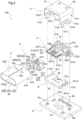
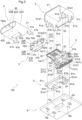
- FIGS. 2 and 3 are exploded perspective views of the receptacle 100 from above and below, respectively.
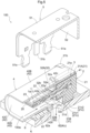
- FIG. 4 is a side cross-sectional view of the receptacle 100 (an IV-IV cross-sectional view of FIG. 1 )
- FIG. 5 is a perspective view in which the receptacle 100 is partially cut out in correspondence with FIG. 4 .
- the substrate K side of the receptacle 100 is defined as a gravity direction side or a lower ("D" in FIG. 1 ) side, the side opposite thereto as an upper ("U" in FIG.
- the receptacle 100 is electrically ground-connected to the substrate K by being fixed to through holes Ka in the substrate K by means of soldering or the like.
- An opening 100a having a flat oval shape is formed on the front side of the receptacle 100, and the receptacle 100 and the plug P are electrically connected to each other by inserting the plug P into the opening 100a.
- the receptacle 100 is a small connector supporting Type-C of the USB standard, and can be inserted into the opening 100a even when the plug P is flipped upside down.
- the receptacle 100 includes contacts 1 that are to be electrically connected to the plug P, a body 2 (an example of a first insulator) that holds the contacts 1, an EMC pad 3 (an example of a first shield member) that covers the body 2, a cover 4 (an example of a second shield member) that comes into contact with an outer face of the EMC pad 3 and covers the body 2, a shell 5 that covers the cover 4, and a spacer 6 (an example of a second insulator) arranged between the cover 4 and the substrate K, outside (below) the cover 4.
- the body 2 and the spacer 6 are molded with an insulating member such as resin, and the contacts 1, the EMC pad 3, the cover 4, and the shell 5 are molded with a conductive member such as metal.
- a plurality of contacts 1 (a total of 16 contacts 1, including eight on the upper face of the body 2 and eight on the lower face in this embodiment) that are held horizontally symmetrically on an upper face and a lower face of the body 2 are provided.
- Each contact 1 has a terminal portion la that is to be electrically connected to a terminal (not shown) of the plug P, a fixed portion 1c that is fixed and electrically connected to the substrate K by means of soldering or the like, and a connecting portion 1b that electrically connects the terminal portion 1a to the fixed portion 1c.
- This connecting portion 1b has a part that is continuous with the terminal portion 1a and accommodated within the body 2, and a part that is bent on the back face side of the body 2 and is continuous with the fixed portion 1c. An end portion of the connecting portion 1b intersects the fixed portion 1c, and the fixed portion 1c is parallel to the substrate K.
- the body 2 is an insulator that is made of resin formed by insert-molding the plurality of contacts 1 and a shield plate 20 that is made of a metal plate and arranged between an upper contact 1 group and a lower contact 1 group in order to shield the pair of contact 1 groups arranged respectively on the upper and lower faces.
- the body 2 includes a base portion 21 having a block shape that internally accommodates a part of the connecting portion 1b of each contact 1 and exposes a part of the connecting portion 1b from the back face, a fitting portion 22 that internally accommodates a boundary part of the connecting portion 1b with the terminal portion 1a and to which a leading end of the plug P is externally fitted, and a protruding portion 23 that exposes the terminal portion 1a from the upper and lower faces and protrudes forward from the fitting portion 22, and the base portion 21, the fitting portion 22, and the protruding portion 23 are integrally formed in this order (specifically, by means of two-color molding).
- a plurality of (three in this embodiment) groove portions 21a that are recessed downward and extend in the front-back direction are formed in the upper face of the base portion 21.
- Restricting portions 21b that restrict backward movement of the cover 4 and forward and downward movement of the shell 5 are formed protruding outward (in the upward, backward, and left-right directions) from back end portions of a pair of side faces in the left-right direction of the base portion 21.
- Each restricting portion 21b includes a front face 21b1 that abuts against a back end of the cover 4, and a side recessed portion 21b2 that engages with the shell 5.
- the shield plate 20 is partially exposed from the pair of side faces in the left-right direction of the base portion 21, and the shield plate 20 and the EMC pad 3 are electrically connected to each other due to exposed parts 20a abutting against an inner face of the EMC pad 3.
- a protruding wall 21c having a cross section perpendicular to the left-right direction that protrudes downward in an L-shape is formed at the center portion of the lower face of the base portion 21.
- This protruding wall 21c includes a first protruding wall 21c1 serving as a part of the lower face, and a second protruding wall 21c2 having a hollow polygonal tubular shape that extends downward (toward the spacer 6 side) from the first protruding wall 21c1 (see FIG. 3 ).
- Apair of block portions 21d that protrude in a block shape are formed on left and right end portions of the lower face of the base portion 21, and column pins 21d1 that are inserted into positioning holes Kb in the substrate K extend downward from the block portions 21d.
- the plurality of insert-molded contacts 1 are exposed from the back face of the base portion 21.
- the fitting portion 22 has a cross section perpendicular to the front-back direction that is formed in a flat oval shape, and a plurality restricting protrusions 22a (a total of four restricting protrusions 22a, including two on the upper face of the fitting portion 22 and two on the lower face in this embodiment) that restrict forward movement of the EMC pad 3 are formed on the upper and lower faces of the fitting portion 22.
- the protruding portion 23 has a rectangular cross section perpendicular to the front-back direction, and the terminal portions 1a of the plurality of insert-molded contacts 1, which are horizontally symmetrical, are exposed from the upper and lower faces of the protruding portion 23. Insert molding is conducted such that the shield plate 20 is sandwiched between the plurality of contacts 1 on the upper face and the plurality contacts 1 on the lower face.
- the EMC pad 3 has a function of shielding the terminals of the plug P and the contacts 1, and is electrically connected to the shield plate 20, the cover 4, and the shell 5.
- the EMC pad 3 is formed by punching and bending a single metal plate, and has an annular portion 31 with a shape following the outer shape of the base portion 21, and a pair of extended portions 32 that extend forward from an upper wall 31A and a lower wall 31B of the annular portion 31.
- the annular portion 31 includes the upper wall 31A, the lower wall 31B, and a pair of side walls 31C that are connected to the upper wall 31A and the lower wall 31B.
- the annular portion 31 has an elastic piece 31a formed at the center portion of the upper wall 31A, and a pair of contact pieces 31b that are electrically connected to the respective quadrangular exposed parts 20a of the shield plate 20 extend backward from the pair of side walls 31C.
- the lower wall 31B of the annular portion 31 includes a flat plate portion 31c (an example of a facing wall) and a bent wall 31d that is vertically bent downward (toward the spacer 6 side) from the flat plate portion 31c.
- a first extended portion 32A on the upper side includes a plurality of (four in this embodiment) bent pieces 32a that are bent from a front end of the upper wall 31Aand extend downward, and one first rectangular portion 32b that is bent from these bent pieces 32a and extends forward.
- a second extended portion 32B (an example of a facing wall) on the lower side includes a step portion 32c that is bent upward from a front end of the lower wall 31B, and a second rectangular portion 32d that is bent from the step portion 32c and extends forward.
- the step portion 32c is bent downward (toward the spacer 6 side) from the second rectangular portion 32d, and connects the second rectangular portion 32d to the flat plate portion 31c.
- the second rectangular portion 32d, the flat plate portion 31c, and the step portion 32c have a shape following the lower faces of the base portion 21 and the fitting portion 22 of the body 2 (see also FIG. 4 ).
- a plurality of cutout recessed portions 32e (a total of four cutout recessed portions 32e, including two on the upper face and two on the lower face in this embodiment), which restrict forward movement of the EMC pad 3 due to the restricting protrusions 22a of the fitting portion 22 abutting against these cutout recessed portions 32e, are formed at front ends of the first rectangular portion 32b and the second rectangular portion 32d.
- the cover 4 has a cross section having a flat oval shape formed by punching and bending a single metal plate.
- the cover 4 has a contact portion 41 that comes into contact with outer faces of the upper wall 31A and the side walls 31C of the annular portion 31 of the EMC pad 3 and is electrically connected to the EMC pad 3, and a tubular portion 42 that extends forward from the contact portion 41 and has an opening 100a into which the plug P is to be inserted.
- the contact portion 41 includes a pair of abutting portions 41a that abut against the front faces 21b1 of the restricting portion 21b of the body 2, and bending pieces 41b that extend backward from the respective abutting portions 41a and are bent to abut against the back face of the body 2.
- the tubular portion 42 has an internal space surrounded by a lower wall 42A that faces the spacer 6, an upper wall 42B that faces the shell 5, and a pair of side walls 42C connected to the lower wall 42A and the upper wall 42B, and the fitting portion 22 and the protruding portion 23 of the body 2 are accommodated in this internal space.
- the spacer 6 faces the lower wall 42A outside the tubular portion 42, and a cutout 42a (an example of a first communicating portion) that has a rectangular shape in a plan view (when viewed in the vertical direction) and is in communication with the outside is provided at a back end of the lower wall 42A (see FIG. 3 ).
- the lower wall 42A is also provided with an inclined wall 42b that is inclined toward the spacer 6 side while extending from the opening 100a side of the cutout 42a toward the side (back side) opposite to the opening 100a side (see FIGS. 4 and 5 ).
- the inclined wall 42b is inclined so as to be separated from the body 2 as the inclined wall 42b extends backward from a front end of the cutout 42a.
- the upper wall 42B has a pair of curved portions 42c that are curved inward from the upper face, enter a pair of groove portions 21a on respective outer sides in the left-right direction, of the three groove portions 21a, of the body 2, and engage between the respective pairs of bent pieces 32a, of the two pairs of (four) bent pieces 32a formed on the EMC pad 3.
- the shell 5 has a U-shaped cross section formed by punching and bending a single metal plate.
- the shell 5 has a cover portion 51 that is electrically connected to the cover 4 by covering outer faces of the upper wall 42B and the side walls 42C of the cover 4 in contact therewith, and a back face portion 52 that is formed by bending a back end of the cover portion 51 and covers the back face of the body 2.
- a pair of side walls of the cover portion 51 has a plurality of (four in this embodiment) leg portions 51a, which extend downward and are inserted into the through holes Ka in the substrate K and soldered.
- a pair of front leg portions 51a have engaging protrusions 51a1, which protrude inward and engage with the spacer 6.
- Each of the two side walls of the cover portion 51 also has a holding portion 51b that holds the spacer 6 by being bent, between the two leg portions 51a arranged in the front-back direction.
- a back-end protruding portion 51c which engages with the corresponding side recessed portion 21b2 of the body 2 to restrict forward movement of the shell 5, extends downward from a back end of each of the two side walls of the cover portion 51.
- the back face portion 52 is spaced apart from the contacts 1 such that the contacts 1 are protected and the impedance of signals traveling through the contacts 1 is constant.
- the spacer 6 is arranged between the cover 4 and the substrate K, and prevents flux used for soldering and solder balls from entering the receptacle 100 when the receptacle 100 is mounted on the substrate K.
- the spacer 6 is formed with a flat plate-shaped member, and has a U-shaped portion 61 having a U-shape in a plan view, and a rectangular recessed portion 62 (an example of a second communicating portion) located at the center portion of a back end of the U-shaped portion 61.
- Engaging grooves 61a with which the holding portions 51b of the cover portion 51 engage by being bent inward, are formed from a pair of outer side faces in the left-right direction of the U-shaped portion 61 to the lower face thereof, and two restricting protrusions 61a1 that restrict movement in the front-back direction of the spacer 6 are provided, protruding in the left-right direction, on respective sides of each engaging groove 61a.
- Engaging recessed portions 61b, with which the engaging protrusions 51a1 of the cover portion 51 engage are formed on the front side of the respective engaging grooves 61a in the pair of side faces of the U-shaped portion 61.
- the U-shaped portion 61 has a pair of straight protruding portions 61c that protrude upward from the pair of side faces, and the side walls 42C of the tubular portion 42 of the cover 4 are arranged so as to be sandwiched between these straight protruding portions 61c.
- the rectangular recessed portion 62 overlaps with the cutout 42a of the lower wall 42A of the tubular portion 42 of the cover 4 in a plan view, and is in communication with the outside and the cutout 42a.
- An inclined face 62a that is inclined toward the substrate K side while extending from the opening 100a side toward the side (back side) opposite to the opening 100a is formed at a front end of the rectangular recessed portion 62.
- the inclined wall 42b of the lower wall 42A of the tubular portion 42 of the cover 4 is arranged along the inclined face 62a.
- the width in the left-right direction of the rectangular recessed portion 62 is larger than the width of the inclined wall 42b of the cover 4, and is smaller than the width of the bent wall 31d of the EMC pad 3.
- the bent wall 31d of the EMC pad 3 abuts against the back side of the U-shaped portion 61, and the inclined wall 42b of the cover 4 enters the front side of the rectangular recessed portion 62.
- a lower end of the bent wall 31d of the EMC pad 3 is formed slightly above a lower face of the rectangular recessed portion 62.
- the substrate K has an open hole Kc that has a rectangular shape in a plan view and overlaps (in communication) with the cutout 42a of the cover 4 and the rectangular recessed portion 62 of the spacer 6 in a plan view.
- the open hole Kc has a larger plane area than the rectangular recessed portion 62.
- the substrate K also have a plurality of (four in this embodiment) through holes Ka, into which the plurality of leg portions 51a of the aforementioned shell 5 are inserted, and a plurality of (two in this embodiment) positioning holes Kb, into which the plurality of column pins 21d1 of the aforementioned body 2 are inserted (see FIGS. 2 and 3 ).
- a method of assembling the receptacle 100 having the above-described configuration is as follows. As shown in FIGS. 2 and 3 , first, the body 2 is manufactured in which the plurality of contacts 1 and the shield plate 20 are insert-molded. When the EMC pad 3 is then externally fitted to the body 2 from the front side, the pair of upper and lower extended portions 32 goes over the restricting protrusions 22a while being elastically deformed, the cutout recessed portions 32e then abuts against the restricting protrusions 22a, and the EMC pad 3 is fixed to the body 2. At this time, the pair of contact pieces 31b of the EMC pad 3 comes into contact with the quadrangular exposed parts 20a of the shield plate 20, and the EMC pad 3 and the shield plate 20 are electrically connected to each other.
- the elastic piece 31a on the upper wall 31A of the EMC pad 3 abuts against the upper wall 42B of the cover 4, and is elastically deformed toward the groove portion 21a at the center, of the three groove portions 21a, of the body 2.
- the inner face of the cover 4 and the outer face of the EMC pad come into contact with each other, and the cover 4 and the EMC pad 3 are electrically connected to each other.
- the pair of curved portions 42c of the cover 4 engage between the respective pairs of bent pieces 32a provided on the two sides of the EMC pad 3, and enter the corresponding groove portions 21a provided on the respective outer sides in the left-right direction of the body 2.
- the pair of bending pieces 41b of the cover 4 are then bent inward such that the bending pieces 41b abut against the back face of the body 2, and thus, the cover 4 is fixed to the EMC pad 3 and the body 2.
- the shell 5 is attached from above to the cover 4, the EMC pad 3, and the body 2, and the spacer 6 is attached thereto from below.
- the engaging protrusions 51a1 of the leg portions 51a of the shell 5 are engaged with the engaging grooves 61b of the spacer 6, and the pair of holding portions 51b of the cover portion 51 are bent inward and engaged with the pair of engaging grooves 61a of the spacer 6.
- the shell 5 and the spacer 6 are fixed to the cover 4, the EMC pad 3, and the body 2, the inner face of the shell 5 and the outer face of the cover 4 come into contact with each other, and the shell 5 and the cover 4 are electrically connected to each other.
- this receptacle 100 When this receptacle 100 is mounted on the substrate K, the plurality of column pins 21d1 of the body 2 are inserted into the plurality of positioning holes Kb, and the plurality of leg portions 51a of the shell 5 are inserted into the plurality of through holes Ka and soldered. Then, the fixed portions 1c of the contacts 1 are soldered to electrodes of the substrate K, and the substrate K and the receptacle 100 are electrically connected to each other (see FIG. 1 ).
- the cutout 42a of the cover 4, the rectangular recessed portion 62 of the spacer 6, and the open hole Kc in the substrate K overlap with each other in a plan view, as shown in FIG. 4 .
- water that enters from the opening 100a of the receptacle 100 flows from the lower wall 42A of the tubular portion 42 of the cover 4 through the inclined wall 42b and is drained to the outside from the cutout 42a, the rectangular recessed portion 62, and the open hole Kc, as indicated by broken arrows in FIG. 5 .
- the water is received by the bent wall 31d of the EMC pad 3 and falls in the gravity direction.
- the EMC pad 3 has the facing walls (the flat plate portion 31c and the second extended portion 32B) that face the cutout 42a, water that enters from the opening 100a of the tubular portion 42 is blocked by the facing walls (the flat plate portion 31c and the second extended portion 32B), and can be drained to the outside from the cutout 42a and the rectangular recessed portion 62, while suppressing entry of the water to the contact 1 side.
- the EMC pad 3 has the bent wall 31d that extends from the flat plate portion 31c, i.e., from an end portion of one facing wall on the opposite side to the opening 100a, and is bent toward the spacer 6 side, water that moves along the facing walls (the flat plate portion 31c and the second extended portion 32B) can be guided to the cutout 42a and the rectangular recessed portion 62 by the bent wall 31d.
- the lower wall 42A of the cover 4 is provided with the inclined wall 42b that is inclined toward the spacer 6 side while extending from the opening 100a side toward the opposite side, the water guided by the inclined wall 42b smoothly falls and can be reliably drained from the cutout 42a and the rectangular recessed portion 62.
- the step portion 32c is provided on the facing walls (the flat plate portion 31c and the second extended portion 32B), water that moves along the facing walls (the flat plate portion 31c and the second extended portion 32B) is guided toward the spacer 6 side by the step portion 32c, and can be smoothly drained from the cutout 42a and the rectangular recessed portion 62.
- the surfaces (at least lower faces) of the facing walls (the flat plate portion 31c and the second extended portion 32B) and the bent wall 31d are hydrophilic, water is likely to be attracted to the facing walls (the flat plate portion 31c and the second extended portion 32B) and the bent wall 31d, and can be reliably drained from the cutout 42a and the rectangular recessed portion 62.
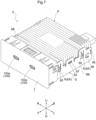
- the charger X includes the above-described receptacle 100, the substrate K on which a plurality of (two in this embodiment) receptacles 100 are mounted, a front shield 7 that covers the receptacles 100 such that the openings 100a are visible from the outside, a bottom shield 8 (an example of a case) that supports the substrate K, and a fin unit 9 that dissipates heat generated from electronic components mounted on the substrate K.
- a lower face of the substrate K i.e., a face thereof on the opposite side to the side on which the receptacles 100 are mounted, is supported by the bottom shield 8.
- the front shield 7 is formed with a conductive member such as metal, and covers the entirety of the receptacles 100 and front parts of the substrate K, the bottom shield 8, and the fin unit 9.
- the bottom shield 8 is formed with a conductive member such as metal, and supports the substrate K and the fin unit 9.
- the bottom shield 8 is formed of a bottom wall 8A, a pair of side walls 8B, a front wall 8C, and a back wall 8D.
- the bottom wall 8A has a plurality of (two in this embodiment) rectangular drain holes 84 for draining water out of the bottom shield 8, and a pair of small holes 84a are formed on the front side of the respective drain holes 84 (see also FIG. 10 ).
- First bent pieces 82 are connected to front ends of the pair of drain holes 84.
- Each of the two side walls 8B has a plurality of (two in this embodiment) engaging pieces 85 that engage with cutouts 91 of the fin unit 9, a plurality of (two in this embodiment) insertion pieces 86 that are inserted into cutouts Kd of the substrate K, a fitting hole 87 into which a corresponding protruding portion 92 of the fin unit 9 is fitted, and a plurality of (two in this embodiment) abutting pieces 88 that abut against the lower face of the lower face of the substrate K.
- the front wall 8C has a pair of second bent pieces 81 that are bent to face the first bent pieces 82.
- the front wall 8C also has a plurality of (two in this embodiment) protruding pieces 89 that are inserted into cutouts Ke of the substrate K.
- the insertion pieces 86 and the protruding pieces 89 are inserted respectively into the plurality of (four in this embodiment) cutouts Kd and the plurality of (two in this embodiment) cutouts Ke of the substrate K to position the substrate K, and the substrate K is supported by the bottom shield 8 due to the plurality of (four in this embodiment) abutting pieces 88 abutting against the lower face of the substrate K.
- the engaging pieces 85 engage with the cutouts 91 of the fin unit 9 to position the fin unit 9, and the fin unit 9 is supported by the bottom shield 8 due to the protruding portions 92 of the fin unit 9 being fitted into the fitting holes 87.
- each first bent piece 82 has a first horizontal portion 82a that extends parallel to the lower face of the substrate K, a first inclined portion 82b that is inclined downward from the first horizontal portion 82a toward the front wall 8C, and a vertical portion 82c perpendicular to the bottom wall 8A.
- the first horizontal portion 82a, the first inclined portion 82b, and the vertical portion 82c are integrally formed.
- Each second bent piece 81 has a second horizontal portion 81a that extends parallel to the lower face of the substrate K, and a second inclined portion 81b that is inclined downward from the second horizontal portion 81a toward the front wall 8C.
- the second horizontal portion 81a and the second inclined portion 81b are integrally formed.
- the substrate K is supported by the first horizontal portion 82a and the second horizontal portion 81a, and a narrow suction path 83 is formed between the first inclined portion 82b of each first bent piece 82 and the second inclined portion 81b of the corresponding second bent piece 81 that face each other.
- This suction path 83 suctions water drained from the open hole Kc in the substrate K, utilizing the capillary phenomenon.
- the water suctioned by the suction path 83 is drained out of the bottom shield 8 from the drain holes 84 in the bottom wall 8A.
- the suction path 83 is provided that suctions water drained from the open hole Kc in the substrate K, utilizing the capillary phenomenon, the water guided to the cutout 42a and the rectangular recessed portion 62 by the bent wall 31d of the receptacle 100 can be forcibly suctioned from the open hole Kc via the suction path 83. Since the water suctioned by the suction path 83 is quickly drained out of the bottom shield 8 from the drain holes 84, it is possible to prevent inconveniences such as water staying in the receptacle 100 and the substrate K.
Landscapes
- Details Of Connecting Devices For Male And Female Coupling (AREA)
- Coupling Device And Connection With Printed Circuit (AREA)
- Connector Housings Or Holding Contact Members (AREA)
Claims (6)
- Steckverbinder (100), umfassend:einen Kontakt (1), der mit einem zu verbindenden Objekt (P) elektrisch zu verbinden ist;einen ersten Isolator (2), der den Kontakt (1) hält;ein erstes Abschirmungselement (3), das den Isolator (2) abdeckt;ein zweites Abschirmungselement (4), das mit einer Außenfläche des ersten Abschirmungselements (3) in Kontakt kommt und einen rohrförmigen Teil (42) hat, der eine Öffnung (100a) hat, in die das zu verbindende Objekt (P) einzuführen ist; undeinen zweiten Isolator (6), der auf einer Außenseite des zweiten Abschirmungselements (4) angeordnet ist,dadurch gekennzeichnet, dassein erster Kommunikationsteil (42a), der mit einer Außenseite in Kommunikation ist, an einer unteren Wand (42A) des rohrförmigen Teils (42) des zweiten Abschirmungselements (4) ausgebildet ist, wobei die untere Wand (42A) zu dem zweiten Isolator (6) hin weist,ein zweiter Kommunikationsteil (62), der mit einer Außenseite und dem ersten Kommunikationsteil (42a) in Kommunikation ist, in dem zweiten Isolator (6) ausgebildet ist, und dassdas erste Abschirmungselement (3) eine plane Wand (31c, 32B), die zu dem ersten Kommunikationsteil (42a) hin weist, und eine gebogene Wand (31d) hat, die von einem Endteil der planen Wand (31c, 32B) auf einer der Öffnung (100a) entgegengesetzten Seite zu der Seite des zweiten Isolators (6) hin gebogen ist.
- Steckverbinder (100) gemäß Anspruch 1,
wobei die untere Wand (42A) des zweiten Abschirmungselements (4) mit einer geneigten Wand (42b) ausgestattet ist, die zu der Seite des zweiten Isolators (6) hin geneigt ist, während sie sich von der Seite der Öffnung (100a) des ersten Kommunikationsteils (42a) zu der entgegengesetzten Seite hin erstreckt. - Steckverbinder (100) gemäß Anspruch 1 oder 2,
wobei ein Stufenteil (32c), der zu der Seite des zweiten Isolators (6) hin gebogen ist, in der planen Wand (31c, 32B) ausgebildet ist. - Steckverbinder (100) gemäß einem der Ansprüche 1 bis 3,
wobei sich die gebogene Wand (31d) bezüglich des zweiten Kommunikationsteils (62) zu der Außenseite hin erstreckt. - Steckverbinder (100) gemäß einem der Ansprüche 1 bis 4,
wobei die plane Wand (31c, 32B) und die gebogene Wand (31d) hydrophile Oberflächen aufweisen. - Steckverbinder-Vorrichtung (X), die den Steckverbinder (100) gemäß einem der Ansprüche 1 bis 5 aufweist, wobei die Vorrichtung umfasst:ein Substrat (K), auf dem der Steckverbinder (100) montiert ist und in dem ein offenes Loch (Kc), das mit dem ersten Kommunikationsteil (42a) und dem zweiten Kommunikationsteil (62) in Kommunikation ist, ausgebildet ist; undein Gehäuse (8), das das Substrat (K) auf einer Seite trägt, die einer Seite entgegengesetzt ist, auf der der Steckverbinder (100) montiert ist,wobei das Gehäuse (8) einen Saugpfad (83) hat, der aus dem offenen Loch (Kc) abgeführtes Wasser unter der Verwendung eines Kapillarphänomens absaugt, und das Wasser über den Saugpfad (83) aus dem Gehäuse (8) abgeführt wird.
Applications Claiming Priority (2)
| Application Number | Priority Date | Filing Date | Title |
|---|---|---|---|
| JP2020157141 | 2020-09-18 | ||
| JP2021014820A JP7462582B2 (ja) | 2020-09-18 | 2021-02-02 | コネクタ及びコネクタ装置 |
Publications (2)
| Publication Number | Publication Date |
|---|---|
| EP3972061A1 EP3972061A1 (de) | 2022-03-23 |
| EP3972061B1 true EP3972061B1 (de) | 2023-03-01 |
Family
ID=77774798
Family Applications (1)
| Application Number | Title | Priority Date | Filing Date |
|---|---|---|---|
| EP21196872.2A Active EP3972061B1 (de) | 2020-09-18 | 2021-09-15 | Verbinder und verbindungsvorrichtung |
Country Status (4)
| Country | Link |
|---|---|
| US (1) | US11670891B2 (de) |
| EP (1) | EP3972061B1 (de) |
| CN (1) | CN114204323A (de) |
| TW (1) | TWI904210B (de) |
Families Citing this family (3)
| Publication number | Priority date | Publication date | Assignee | Title |
|---|---|---|---|---|
| EP3648264A1 (de) * | 2018-10-31 | 2020-05-06 | Koninklijke Philips N.V. | Elektrischer verbinder mit usb-serie ein kontaktblockabstand |
| DE102020130915B3 (de) * | 2020-11-23 | 2022-01-27 | Harting Electric Gmbh & Co. Kg | Verbessertes Steckverbindermodul für einen modularen Industriesteckverbinder und Verfahren zur Herstellung eines solchen Steckverbindermoduls |
| US20230327364A1 (en) * | 2022-04-12 | 2023-10-12 | Amphenol East Asia Electronic Technology (Shen Zhen) Co., Ltd. | Type-c female socket iron case |
Family Cites Families (4)
| Publication number | Priority date | Publication date | Assignee | Title |
|---|---|---|---|---|
| CN104112968B (zh) | 2013-04-18 | 2016-07-13 | 富士康(昆山)电脑接插件有限公司 | 插座电连接器及其制造方法 |
| JP6150068B2 (ja) * | 2013-10-23 | 2017-06-21 | Smk株式会社 | コネクタ |
| TWM493184U (zh) * | 2014-08-18 | 2015-01-01 | Chant Sincere Co Ltd | 連接器 |
| WO2018168352A1 (ja) * | 2017-03-13 | 2018-09-20 | 株式会社村田製作所 | レセプタクル |
-
2021
- 2021-08-05 TW TW110128927A patent/TWI904210B/zh active
- 2021-09-14 US US17/474,483 patent/US11670891B2/en active Active
- 2021-09-15 EP EP21196872.2A patent/EP3972061B1/de active Active
- 2021-09-17 CN CN202111092882.5A patent/CN114204323A/zh active Pending
Also Published As
| Publication number | Publication date |
|---|---|
| TWI904210B (zh) | 2025-11-11 |
| EP3972061A1 (de) | 2022-03-23 |
| CN114204323A (zh) | 2022-03-18 |
| US20220094102A1 (en) | 2022-03-24 |
| US11670891B2 (en) | 2023-06-06 |
| KR20220037952A (ko) | 2022-03-25 |
| TW202228342A (zh) | 2022-07-16 |
Similar Documents
| Publication | Publication Date | Title |
|---|---|---|
| US7686622B2 (en) | Plug connector with mating protection | |
| US10096947B2 (en) | Electrical connector and electrical device assembled with the same therein | |
| US9106024B2 (en) | Electrical connector with a metal plate for preventing electromagnetic interference | |
| US7108554B2 (en) | Electrical connector with shielding member | |
| EP3972061A1 (de) | Verbinder und verbindungsvorrichtung | |
| US7086902B1 (en) | Connector with improved shielding member | |
| US11146004B2 (en) | Connector assembly | |
| USRE43427E1 (en) | Plug connector with mating protection | |
| US6814612B1 (en) | Shielded electrical connector | |
| US7128607B2 (en) | Socket connector with reliable shielding member | |
| KR20070025948A (ko) | 커넥터, 커넥터용 리셉터클 및 커넥터용 플러그 | |
| US7232316B2 (en) | Electrical connector with improved shielding means | |
| JP2021174770A (ja) | 基板側コネクタおよびコネクタアセンブリ | |
| JP7606661B2 (ja) | 基板用コネクタおよび機器 | |
| US20180151985A1 (en) | Electrical connector having shielding plate retained tightly thereto | |
| US6926540B1 (en) | Transmission module assembly having printed circuit board | |
| US6193552B1 (en) | Electrical connector | |
| JP7713162B2 (ja) | 基板用コネクタおよび機器 | |
| US7661990B1 (en) | Electrical connector | |
| US6267624B1 (en) | Electrical connector | |
| US9685740B1 (en) | Waterproof connector | |
| JP6112937B2 (ja) | 中継電気コネクタ | |
| JP7462582B2 (ja) | コネクタ及びコネクタ装置 | |
| JP4028439B2 (ja) | 回路基板内蔵型コネクタ | |
| KR102962131B1 (ko) | 커넥터 및 커넥터 장치 |
Legal Events
| Date | Code | Title | Description |
|---|---|---|---|
| PUAI | Public reference made under article 153(3) epc to a published international application that has entered the european phase |
Free format text: ORIGINAL CODE: 0009012 |
|
| STAA | Information on the status of an ep patent application or granted ep patent |
Free format text: STATUS: THE APPLICATION HAS BEEN PUBLISHED |
|
| AK | Designated contracting states |
Kind code of ref document: A1 Designated state(s): AL AT BE BG CH CY CZ DE DK EE ES FI FR GB GR HR HU IE IS IT LI LT LU LV MC MK MT NL NO PL PT RO RS SE SI SK SM TR |
|
| STAA | Information on the status of an ep patent application or granted ep patent |
Free format text: STATUS: REQUEST FOR EXAMINATION WAS MADE |
|
| 17P | Request for examination filed |
Effective date: 20220530 |
|
| RBV | Designated contracting states (corrected) |
Designated state(s): AL AT BE BG CH CY CZ DE DK EE ES FI FR GB GR HR HU IE IS IT LI LT LU LV MC MK MT NL NO PL PT RO RS SE SI SK SM TR |
|
| GRAP | Despatch of communication of intention to grant a patent |
Free format text: ORIGINAL CODE: EPIDOSNIGR1 |
|
| STAA | Information on the status of an ep patent application or granted ep patent |
Free format text: STATUS: GRANT OF PATENT IS INTENDED |
|
| RIC1 | Information provided on ipc code assigned before grant |
Ipc: H01R 12/72 20110101ALN20220906BHEP Ipc: H01R 107/00 20060101ALN20220906BHEP Ipc: H01R 24/60 20110101ALN20220906BHEP Ipc: H05K 5/02 20060101ALN20220906BHEP Ipc: H01R 13/6594 20110101ALN20220906BHEP Ipc: H01R 13/502 20060101ALI20220906BHEP Ipc: H01R 13/52 20060101AFI20220906BHEP |
|
| INTG | Intention to grant announced |
Effective date: 20220923 |
|
| GRAS | Grant fee paid |
Free format text: ORIGINAL CODE: EPIDOSNIGR3 |
|
| GRAA | (expected) grant |
Free format text: ORIGINAL CODE: 0009210 |
|
| STAA | Information on the status of an ep patent application or granted ep patent |
Free format text: STATUS: THE PATENT HAS BEEN GRANTED |
|
| AK | Designated contracting states |
Kind code of ref document: B1 Designated state(s): AL AT BE BG CH CY CZ DE DK EE ES FI FR GB GR HR HU IE IS IT LI LT LU LV MC MK MT NL NO PL PT RO RS SE SI SK SM TR |
|
| REG | Reference to a national code |
Ref country code: GB Ref legal event code: FG4D |
|
| REG | Reference to a national code |
Ref country code: CH Ref legal event code: EP Ref country code: AT Ref legal event code: REF Ref document number: 1551662 Country of ref document: AT Kind code of ref document: T Effective date: 20230315 |
|
| REG | Reference to a national code |
Ref country code: DE Ref legal event code: R096 Ref document number: 602021001517 Country of ref document: DE |
|
| REG | Reference to a national code |
Ref country code: IE Ref legal event code: FG4D |
|
| REG | Reference to a national code |
Ref country code: LT Ref legal event code: MG9D |
|
| REG | Reference to a national code |
Ref country code: NL Ref legal event code: MP Effective date: 20230301 |
|
| PG25 | Lapsed in a contracting state [announced via postgrant information from national office to epo] |
Ref country code: RS Free format text: LAPSE BECAUSE OF FAILURE TO SUBMIT A TRANSLATION OF THE DESCRIPTION OR TO PAY THE FEE WITHIN THE PRESCRIBED TIME-LIMIT Effective date: 20230301 Ref country code: NO Free format text: LAPSE BECAUSE OF FAILURE TO SUBMIT A TRANSLATION OF THE DESCRIPTION OR TO PAY THE FEE WITHIN THE PRESCRIBED TIME-LIMIT Effective date: 20230601 Ref country code: LV Free format text: LAPSE BECAUSE OF FAILURE TO SUBMIT A TRANSLATION OF THE DESCRIPTION OR TO PAY THE FEE WITHIN THE PRESCRIBED TIME-LIMIT Effective date: 20230301 Ref country code: LT Free format text: LAPSE BECAUSE OF FAILURE TO SUBMIT A TRANSLATION OF THE DESCRIPTION OR TO PAY THE FEE WITHIN THE PRESCRIBED TIME-LIMIT Effective date: 20230301 Ref country code: HR Free format text: LAPSE BECAUSE OF FAILURE TO SUBMIT A TRANSLATION OF THE DESCRIPTION OR TO PAY THE FEE WITHIN THE PRESCRIBED TIME-LIMIT Effective date: 20230301 Ref country code: ES Free format text: LAPSE BECAUSE OF FAILURE TO SUBMIT A TRANSLATION OF THE DESCRIPTION OR TO PAY THE FEE WITHIN THE PRESCRIBED TIME-LIMIT Effective date: 20230301 |
|
| REG | Reference to a national code |
Ref country code: AT Ref legal event code: MK05 Ref document number: 1551662 Country of ref document: AT Kind code of ref document: T Effective date: 20230301 |
|
| PG25 | Lapsed in a contracting state [announced via postgrant information from national office to epo] |
Ref country code: SE Free format text: LAPSE BECAUSE OF FAILURE TO SUBMIT A TRANSLATION OF THE DESCRIPTION OR TO PAY THE FEE WITHIN THE PRESCRIBED TIME-LIMIT Effective date: 20230301 Ref country code: PL Free format text: LAPSE BECAUSE OF FAILURE TO SUBMIT A TRANSLATION OF THE DESCRIPTION OR TO PAY THE FEE WITHIN THE PRESCRIBED TIME-LIMIT Effective date: 20230301 Ref country code: NL Free format text: LAPSE BECAUSE OF FAILURE TO SUBMIT A TRANSLATION OF THE DESCRIPTION OR TO PAY THE FEE WITHIN THE PRESCRIBED TIME-LIMIT Effective date: 20230301 Ref country code: GR Free format text: LAPSE BECAUSE OF FAILURE TO SUBMIT A TRANSLATION OF THE DESCRIPTION OR TO PAY THE FEE WITHIN THE PRESCRIBED TIME-LIMIT Effective date: 20230602 Ref country code: FI Free format text: LAPSE BECAUSE OF FAILURE TO SUBMIT A TRANSLATION OF THE DESCRIPTION OR TO PAY THE FEE WITHIN THE PRESCRIBED TIME-LIMIT Effective date: 20230301 |
|
| PG25 | Lapsed in a contracting state [announced via postgrant information from national office to epo] |
Ref country code: SM Free format text: LAPSE BECAUSE OF FAILURE TO SUBMIT A TRANSLATION OF THE DESCRIPTION OR TO PAY THE FEE WITHIN THE PRESCRIBED TIME-LIMIT Effective date: 20230301 Ref country code: RO Free format text: LAPSE BECAUSE OF FAILURE TO SUBMIT A TRANSLATION OF THE DESCRIPTION OR TO PAY THE FEE WITHIN THE PRESCRIBED TIME-LIMIT Effective date: 20230301 Ref country code: PT Free format text: LAPSE BECAUSE OF FAILURE TO SUBMIT A TRANSLATION OF THE DESCRIPTION OR TO PAY THE FEE WITHIN THE PRESCRIBED TIME-LIMIT Effective date: 20230703 Ref country code: EE Free format text: LAPSE BECAUSE OF FAILURE TO SUBMIT A TRANSLATION OF THE DESCRIPTION OR TO PAY THE FEE WITHIN THE PRESCRIBED TIME-LIMIT Effective date: 20230301 Ref country code: CZ Free format text: LAPSE BECAUSE OF FAILURE TO SUBMIT A TRANSLATION OF THE DESCRIPTION OR TO PAY THE FEE WITHIN THE PRESCRIBED TIME-LIMIT Effective date: 20230301 Ref country code: AT Free format text: LAPSE BECAUSE OF FAILURE TO SUBMIT A TRANSLATION OF THE DESCRIPTION OR TO PAY THE FEE WITHIN THE PRESCRIBED TIME-LIMIT Effective date: 20230301 |
|
| PG25 | Lapsed in a contracting state [announced via postgrant information from national office to epo] |
Ref country code: SK Free format text: LAPSE BECAUSE OF FAILURE TO SUBMIT A TRANSLATION OF THE DESCRIPTION OR TO PAY THE FEE WITHIN THE PRESCRIBED TIME-LIMIT Effective date: 20230301 Ref country code: IS Free format text: LAPSE BECAUSE OF FAILURE TO SUBMIT A TRANSLATION OF THE DESCRIPTION OR TO PAY THE FEE WITHIN THE PRESCRIBED TIME-LIMIT Effective date: 20230701 |
|
| REG | Reference to a national code |
Ref country code: DE Ref legal event code: R097 Ref document number: 602021001517 Country of ref document: DE |
|
| PLBE | No opposition filed within time limit |
Free format text: ORIGINAL CODE: 0009261 |
|
| STAA | Information on the status of an ep patent application or granted ep patent |
Free format text: STATUS: NO OPPOSITION FILED WITHIN TIME LIMIT |
|
| PG25 | Lapsed in a contracting state [announced via postgrant information from national office to epo] |
Ref country code: SI Free format text: LAPSE BECAUSE OF FAILURE TO SUBMIT A TRANSLATION OF THE DESCRIPTION OR TO PAY THE FEE WITHIN THE PRESCRIBED TIME-LIMIT Effective date: 20230301 Ref country code: DK Free format text: LAPSE BECAUSE OF FAILURE TO SUBMIT A TRANSLATION OF THE DESCRIPTION OR TO PAY THE FEE WITHIN THE PRESCRIBED TIME-LIMIT Effective date: 20230301 |
|
| 26N | No opposition filed |
Effective date: 20231204 |
|
| PG25 | Lapsed in a contracting state [announced via postgrant information from national office to epo] |
Ref country code: LU Free format text: LAPSE BECAUSE OF NON-PAYMENT OF DUE FEES Effective date: 20230915 |
|
| REG | Reference to a national code |
Ref country code: BE Ref legal event code: MM Effective date: 20230930 |
|
| PG25 | Lapsed in a contracting state [announced via postgrant information from national office to epo] |
Ref country code: LU Free format text: LAPSE BECAUSE OF NON-PAYMENT OF DUE FEES Effective date: 20230915 Ref country code: IT Free format text: LAPSE BECAUSE OF FAILURE TO SUBMIT A TRANSLATION OF THE DESCRIPTION OR TO PAY THE FEE WITHIN THE PRESCRIBED TIME-LIMIT Effective date: 20230301 Ref country code: MC Free format text: LAPSE BECAUSE OF FAILURE TO SUBMIT A TRANSLATION OF THE DESCRIPTION OR TO PAY THE FEE WITHIN THE PRESCRIBED TIME-LIMIT Effective date: 20230301 |
|
| REG | Reference to a national code |
Ref country code: IE Ref legal event code: MM4A |
|
| PG25 | Lapsed in a contracting state [announced via postgrant information from national office to epo] |
Ref country code: IE Free format text: LAPSE BECAUSE OF NON-PAYMENT OF DUE FEES Effective date: 20230915 |
|
| PG25 | Lapsed in a contracting state [announced via postgrant information from national office to epo] |
Ref country code: IE Free format text: LAPSE BECAUSE OF NON-PAYMENT OF DUE FEES Effective date: 20230915 |
|
| PG25 | Lapsed in a contracting state [announced via postgrant information from national office to epo] |
Ref country code: BE Free format text: LAPSE BECAUSE OF NON-PAYMENT OF DUE FEES Effective date: 20230930 |
|
| PG25 | Lapsed in a contracting state [announced via postgrant information from national office to epo] |
Ref country code: BG Free format text: LAPSE BECAUSE OF FAILURE TO SUBMIT A TRANSLATION OF THE DESCRIPTION OR TO PAY THE FEE WITHIN THE PRESCRIBED TIME-LIMIT Effective date: 20230301 |
|
| PG25 | Lapsed in a contracting state [announced via postgrant information from national office to epo] |
Ref country code: BG Free format text: LAPSE BECAUSE OF FAILURE TO SUBMIT A TRANSLATION OF THE DESCRIPTION OR TO PAY THE FEE WITHIN THE PRESCRIBED TIME-LIMIT Effective date: 20230301 |
|
| REG | Reference to a national code |
Ref country code: CH Ref legal event code: PL |
|
| PG25 | Lapsed in a contracting state [announced via postgrant information from national office to epo] |
Ref country code: CH Free format text: LAPSE BECAUSE OF NON-PAYMENT OF DUE FEES Effective date: 20240930 |
|
| PG25 | Lapsed in a contracting state [announced via postgrant information from national office to epo] |
Ref country code: CY Free format text: LAPSE BECAUSE OF FAILURE TO SUBMIT A TRANSLATION OF THE DESCRIPTION OR TO PAY THE FEE WITHIN THE PRESCRIBED TIME-LIMIT; INVALID AB INITIO Effective date: 20210915 |
|
| PG25 | Lapsed in a contracting state [announced via postgrant information from national office to epo] |
Ref country code: HU Free format text: LAPSE BECAUSE OF FAILURE TO SUBMIT A TRANSLATION OF THE DESCRIPTION OR TO PAY THE FEE WITHIN THE PRESCRIBED TIME-LIMIT; INVALID AB INITIO Effective date: 20210915 |
|
| PGFP | Annual fee paid to national office [announced via postgrant information from national office to epo] |
Ref country code: DE Payment date: 20250718 Year of fee payment: 5 |
|
| PGFP | Annual fee paid to national office [announced via postgrant information from national office to epo] |
Ref country code: GB Payment date: 20250923 Year of fee payment: 5 |
|
| PGFP | Annual fee paid to national office [announced via postgrant information from national office to epo] |
Ref country code: FR Payment date: 20250926 Year of fee payment: 5 |
|
| PG25 | Lapsed in a contracting state [announced via postgrant information from national office to epo] |
Ref country code: TR Free format text: LAPSE BECAUSE OF FAILURE TO SUBMIT A TRANSLATION OF THE DESCRIPTION OR TO PAY THE FEE WITHIN THE PRESCRIBED TIME-LIMIT Effective date: 20230301 |