EP3970135B1 - Pixelschaltung und pixelsteuerungsverfahren - Google Patents
Pixelschaltung und pixelsteuerungsverfahren Download PDFInfo
- Publication number
- EP3970135B1 EP3970135B1 EP19931075.6A EP19931075A EP3970135B1 EP 3970135 B1 EP3970135 B1 EP 3970135B1 EP 19931075 A EP19931075 A EP 19931075A EP 3970135 B1 EP3970135 B1 EP 3970135B1
- Authority
- EP
- European Patent Office
- Prior art keywords
- gate
- transistor
- signal
- voltage
- photosensor
- Prior art date
- Legal status (The legal status is an assumption and is not a legal conclusion. Google has not performed a legal analysis and makes no representation as to the accuracy of the status listed.)
- Active
Links
Images





Classifications
-
- G—PHYSICS
- G09—EDUCATION; CRYPTOGRAPHY; DISPLAY; ADVERTISING; SEALS
- G09G—ARRANGEMENTS OR CIRCUITS FOR CONTROL OF INDICATING DEVICES USING STATIC MEANS TO PRESENT VARIABLE INFORMATION
- G09G3/00—Control arrangements or circuits, of interest only in connection with visual indicators other than cathode-ray tubes
- G09G3/20—Control arrangements or circuits, of interest only in connection with visual indicators other than cathode-ray tubes for presentation of an assembly of a number of characters, e.g. a page, by composing the assembly by combination of individual elements arranged in a matrix no fixed position being assigned to or needed to be assigned to the individual characters or partial characters
- G09G3/22—Control arrangements or circuits, of interest only in connection with visual indicators other than cathode-ray tubes for presentation of an assembly of a number of characters, e.g. a page, by composing the assembly by combination of individual elements arranged in a matrix no fixed position being assigned to or needed to be assigned to the individual characters or partial characters using controlled light sources
- G09G3/30—Control arrangements or circuits, of interest only in connection with visual indicators other than cathode-ray tubes for presentation of an assembly of a number of characters, e.g. a page, by composing the assembly by combination of individual elements arranged in a matrix no fixed position being assigned to or needed to be assigned to the individual characters or partial characters using controlled light sources using electroluminescent panels
- G09G3/32—Control arrangements or circuits, of interest only in connection with visual indicators other than cathode-ray tubes for presentation of an assembly of a number of characters, e.g. a page, by composing the assembly by combination of individual elements arranged in a matrix no fixed position being assigned to or needed to be assigned to the individual characters or partial characters using controlled light sources using electroluminescent panels semiconductive, e.g. using light-emitting diodes [LED]
- G09G3/3208—Control arrangements or circuits, of interest only in connection with visual indicators other than cathode-ray tubes for presentation of an assembly of a number of characters, e.g. a page, by composing the assembly by combination of individual elements arranged in a matrix no fixed position being assigned to or needed to be assigned to the individual characters or partial characters using controlled light sources using electroluminescent panels semiconductive, e.g. using light-emitting diodes [LED] organic, e.g. using organic light-emitting diodes [OLED]
- G09G3/3225—Control arrangements or circuits, of interest only in connection with visual indicators other than cathode-ray tubes for presentation of an assembly of a number of characters, e.g. a page, by composing the assembly by combination of individual elements arranged in a matrix no fixed position being assigned to or needed to be assigned to the individual characters or partial characters using controlled light sources using electroluminescent panels semiconductive, e.g. using light-emitting diodes [LED] organic, e.g. using organic light-emitting diodes [OLED] using an active matrix
- G09G3/3233—Control arrangements or circuits, of interest only in connection with visual indicators other than cathode-ray tubes for presentation of an assembly of a number of characters, e.g. a page, by composing the assembly by combination of individual elements arranged in a matrix no fixed position being assigned to or needed to be assigned to the individual characters or partial characters using controlled light sources using electroluminescent panels semiconductive, e.g. using light-emitting diodes [LED] organic, e.g. using organic light-emitting diodes [OLED] using an active matrix with pixel circuitry controlling the current through the light-emitting element
-
- G—PHYSICS
- G09—EDUCATION; CRYPTOGRAPHY; DISPLAY; ADVERTISING; SEALS
- G09G—ARRANGEMENTS OR CIRCUITS FOR CONTROL OF INDICATING DEVICES USING STATIC MEANS TO PRESENT VARIABLE INFORMATION
- G09G2300/00—Aspects of the constitution of display devices
- G09G2300/08—Active matrix structure, i.e. with use of active elements, inclusive of non-linear two terminal elements, in the pixels together with light emitting or modulating elements
- G09G2300/0809—Several active elements per pixel in active matrix panels
- G09G2300/0819—Several active elements per pixel in active matrix panels used for counteracting undesired variations, e.g. feedback or autozeroing
-
- G—PHYSICS
- G09—EDUCATION; CRYPTOGRAPHY; DISPLAY; ADVERTISING; SEALS
- G09G—ARRANGEMENTS OR CIRCUITS FOR CONTROL OF INDICATING DEVICES USING STATIC MEANS TO PRESENT VARIABLE INFORMATION
- G09G2300/00—Aspects of the constitution of display devices
- G09G2300/08—Active matrix structure, i.e. with use of active elements, inclusive of non-linear two terminal elements, in the pixels together with light emitting or modulating elements
- G09G2300/0809—Several active elements per pixel in active matrix panels
- G09G2300/0842—Several active elements per pixel in active matrix panels forming a memory circuit, e.g. a dynamic memory with one capacitor
- G09G2300/0861—Several active elements per pixel in active matrix panels forming a memory circuit, e.g. a dynamic memory with one capacitor with additional control of the display period without amending the charge stored in a pixel memory, e.g. by means of additional select electrodes
-
- G—PHYSICS
- G09—EDUCATION; CRYPTOGRAPHY; DISPLAY; ADVERTISING; SEALS
- G09G—ARRANGEMENTS OR CIRCUITS FOR CONTROL OF INDICATING DEVICES USING STATIC MEANS TO PRESENT VARIABLE INFORMATION
- G09G2310/00—Command of the display device
- G09G2310/02—Addressing, scanning or driving the display screen or processing steps related thereto
- G09G2310/0243—Details of the generation of driving signals
- G09G2310/0251—Precharge or discharge of pixel before applying new pixel voltage
-
- G—PHYSICS
- G09—EDUCATION; CRYPTOGRAPHY; DISPLAY; ADVERTISING; SEALS
- G09G—ARRANGEMENTS OR CIRCUITS FOR CONTROL OF INDICATING DEVICES USING STATIC MEANS TO PRESENT VARIABLE INFORMATION
- G09G2310/00—Command of the display device
- G09G2310/02—Addressing, scanning or driving the display screen or processing steps related thereto
- G09G2310/0262—The addressing of the pixel, in a display other than an active matrix LCD, involving the control of two or more scan electrodes or two or more data electrodes, e.g. pixel voltage dependent on signals of two data electrodes
-
- G—PHYSICS
- G09—EDUCATION; CRYPTOGRAPHY; DISPLAY; ADVERTISING; SEALS
- G09G—ARRANGEMENTS OR CIRCUITS FOR CONTROL OF INDICATING DEVICES USING STATIC MEANS TO PRESENT VARIABLE INFORMATION
- G09G2310/00—Command of the display device
- G09G2310/08—Details of timing specific for flat panels, other than clock recovery
-
- G—PHYSICS
- G09—EDUCATION; CRYPTOGRAPHY; DISPLAY; ADVERTISING; SEALS
- G09G—ARRANGEMENTS OR CIRCUITS FOR CONTROL OF INDICATING DEVICES USING STATIC MEANS TO PRESENT VARIABLE INFORMATION
- G09G2330/00—Aspects of power supply; Aspects of display protection and defect management
- G09G2330/02—Details of power systems and of start or stop of display operation
- G09G2330/021—Power management, e.g. power saving
-
- G—PHYSICS
- G09—EDUCATION; CRYPTOGRAPHY; DISPLAY; ADVERTISING; SEALS
- G09G—ARRANGEMENTS OR CIRCUITS FOR CONTROL OF INDICATING DEVICES USING STATIC MEANS TO PRESENT VARIABLE INFORMATION
- G09G2354/00—Aspects of interface with display user
-
- G—PHYSICS
- G09—EDUCATION; CRYPTOGRAPHY; DISPLAY; ADVERTISING; SEALS
- G09G—ARRANGEMENTS OR CIRCUITS FOR CONTROL OF INDICATING DEVICES USING STATIC MEANS TO PRESENT VARIABLE INFORMATION
- G09G2360/00—Aspects of the architecture of display systems
- G09G2360/14—Detecting light within display terminals, e.g. using a single or a plurality of photosensors
-
- G—PHYSICS
- G09—EDUCATION; CRYPTOGRAPHY; DISPLAY; ADVERTISING; SEALS
- G09G—ARRANGEMENTS OR CIRCUITS FOR CONTROL OF INDICATING DEVICES USING STATIC MEANS TO PRESENT VARIABLE INFORMATION
- G09G2360/00—Aspects of the architecture of display systems
- G09G2360/14—Detecting light within display terminals, e.g. using a single or a plurality of photosensors
- G09G2360/144—Detecting light within display terminals, e.g. using a single or a plurality of photosensors the light being ambient light
-
- G—PHYSICS
- G09—EDUCATION; CRYPTOGRAPHY; DISPLAY; ADVERTISING; SEALS
- G09G—ARRANGEMENTS OR CIRCUITS FOR CONTROL OF INDICATING DEVICES USING STATIC MEANS TO PRESENT VARIABLE INFORMATION
- G09G2360/00—Aspects of the architecture of display systems
- G09G2360/14—Detecting light within display terminals, e.g. using a single or a plurality of photosensors
- G09G2360/145—Detecting light within display terminals, e.g. using a single or a plurality of photosensors the light originating from the display screen
- G09G2360/147—Detecting light within display terminals, e.g. using a single or a plurality of photosensors the light originating from the display screen the originated light output being determined for each pixel
- G09G2360/148—Detecting light within display terminals, e.g. using a single or a plurality of photosensors the light originating from the display screen the originated light output being determined for each pixel the light being detected by light detection means within each pixel
Definitions
- the present disclosure relates to a pixel circuit and a pixel control method therefor, and, more particularly, to a pixel circuit which is applied to an organic EL display and is combined with a photosensor, and a control method for a pixel circuit.
- a conventionally known organic electroluminescent (EL) display is a flat panel display that uses an organic light emitting diode (OLED) as a display element and drives the OLED by current to emit light.
- OLED organic light emitting diode
- a driving transistor causes the current to flow to the OLED, so that the characteristics of the driving transistor are important.
- a thin film transistor (TFT) used as a driving transistor has a problem such that the threshold voltage is not uniform, and even if same data is input, different currents are generated to cause variations in luminance. Therefore, various pixel unit drive circuits are designed to compensate for variations in threshold voltage of individual TFTs.
- a 6T1C (six transistors and one capacitor) circuit and a 7T1C (seven transistors and one capacitor) circuit are provided for each pixel as pixel unit drive circuits used for OLEDs of portable terminals.
- a large number of transistors implemented for one pixel are one factor to complicate the pixel circuit.
- CMOS image sensor includes an active pixel sensor (APS) that increases the gain of signals on a pixel-by-pixel basis to increase the signal-to-noise ratio (S/N ratio) of the photosensor.
- APS active pixel sensor
- the structure of the APS includes, for each pixel, three TFTs: a transistor for resetting the voltage of a photodiode (PD), a transistor for amplifying the gain, and a transistor for reading out the signal.
- an organic EL display including a pixel circuit combined with a photosensor In a case of forming an organic EL display including a pixel circuit combined with a photosensor, one APS is combined with a single pixel of an OLED. Since a pixel circuit is configured by implementing a pixel unit drive circuit such as a 6T1C circuit or a 7T1C circuit together with an APS structure having a photosensor. Therefore, the circuit configuration becomes more complicated, thus requiring a larger footprint. This results in a reduction in the resolution of the display.
- Document US9536472B2 discloses a 7T1C pixel circuit.
- Document US10074710B2 discloses a 7T1C pixel circuit with dual / double gate transistors.
- Document CN108735782A discloses a 2T1C pixel circuit with a cathode of a photodiode connected to a second gate of a select transistor.
- a pixel unit drive circuit as claimed in independent device claim 1, which has a simple circuit structure, and could be used to reduce complexity of a pixel circuit that includes this pixel unit drive circuit.
- a pixel control method as claimed in independent method claim 6, capable of quickly controlling sub pixels with photosensors is provided.
- a pixel circuit having: a switching transistor for switching a data signal to be applied to a data line; a driving transistor for supplying a drive current to an organic light emitting diode (OLED) according to a charge voltage corresponding to the data signal; a compensation transistor for compensating for a threshold voltage of the driving transistor,
- OLED organic light emitting diode
- the first aspect allows a photosensor having a desired sensitivity to be implemented into a pixel circuit without reducing the implementation efficiency.
- a scan signal for turning on the dual gate transistor is applied to the second gate to charge the data signal applied to the data line, and an adaptively controlled scan signal is applied to the second gate to read out a signal from the photosensor from the data line.
- the dual gate transistor operates as a readout transistor for reading out a signal from the photosensor as well as an amplification transistor for amplifying a signal, and can ensure fast signal reading from a photosensor in a combination of the OLED and the photosensor.
- the adaptively controlled scan signal is a voltage of a level between a high level and a low level, thereby a voltage of the second gate is varied according to charges stored by the photosensor, and a current according to a voltage applied to the first gate flows through the data line.
- the adaptively controlled scan signal is controlled according to an intensity of environmental light.
- the photosensor can be operated as a highly sensitive photosensor which is not affected by ambient environmental light.
- a pixel control method for a pixel circuit of the first aspect includes:
- the second aspect allows a photosensor to be implemented into a pixel circuit without reducing the implementation efficiency and also ensures that a desired sensitivity is obtained from the photosensor.
- the causing the dual gate transistor to operate as a switch for switching the data signal applies a scan signal for turning on the dual gate transistor to the second gate to charge the data signal applied to the data line.
- the reading out a signal from the photosensor from the data line applies a voltage of a level between a high level and a low level to the second gate, thereby a voltage of the second gate is varied according to charges stored by the photosensor, and a current according to a voltage applied to the first gate flows through the data line.
- the dual gate transistor operates as a readout transistor for reading out a signal from the photosensor as well as an amplification transistor for amplifying a signal, and can ensure fast signal reading from a photosensor in a combination of the OLED and the photosensor.
- the reading out a signal from the photosensor from the data line applies a scan signal adaptively controlled according to an intensity of environmental light to the second gate.
- the photosensor can be operated as a highly sensitive photosensor which is not affected by ambient environmental light.
- a display device including a plurality of pixel units and a cover plate, the plurality of pixel units are all on the same side of the cover plate, wherein each pixel unit includes the above-mentioned pixel circuit.
- Fig. 1 is a diagram showing an example of the configuration of a 6T1C circuit which is a pixel unit drive circuit used in an OLED.
- This pixel unit drive circuit 1 drives and controls pixels for each pixel unit; one subpixel corresponds to a pixel unit in the following description.
- This pixel unit drive circuit 1 includes one OLED 31, six transistors T11 to T16, and one capacitor C11.
- One OLED 31 corresponds to a subpixel of one color in red (R), green (G) and blue (B) subpixels constituting one pixel.
- the pixel unit drive circuit 1 includes the switching transistor T12 for, in response to a scan (gate) signal Gate (n) applied to an nth scan line, switching a data signal of a voltage level V data applied to the corresponding data line.
- the pixel unit drive circuit 1 also includes the driving transistor T13 that supplies a drive current for the OLED 31 according to a charge voltage corresponding to a data signal input to the driving transistor T13 via the switching transistor T12, and the compensation transistor T15 for compensating for a threshold voltage of the driving transistor T13.
- the pixel unit drive circuit 1 further includes the capacitor C11 for storing the data signal applied to the gate of the driving transistor T13, and the OLED 31 that emits light corresponding to the applied drive current.
- the pixel unit drive circuit 1 includes the switching transistor T11 for supplying a power supply voltage V dd to the driving transistor T13 in response to an emission signal Em, and the switching transistor T16 for supplying the drive current input via the driving transistor T13 to the OLED 31 in response to the emission signal Em.
- the transistors T11 to T16 are configured as a p-type thin film transistor (TFT).
- the switching transistor T12 has a gate to which the nth scan signal Gate(n) applied to the corresponding scan line is applied, a source to which a data signal of a voltage level V data applied to the corresponding data line is applied, and a drain connected to a source of the driving transistor T13.
- the driving transistor T13 has a gate connected to one terminal of the capacitor C11, and a drain connected to an anode terminal of the OLED 31 via the switching transistor T16.
- the compensation transistor T15 has a drain connected to the gate of the driving transistor T13, a source connected to the drain of the driving transistor T13, and a gate to which the scan signal Gate (n) is applied.
- the power supply voltage V dd of a high level is supplied from the corresponding power supply to the other terminal of the capacitor C11.
- the switching transistor T11 has a gate to which the emission signal Em is applied, a source to which the power supply voltage V dd is applied through the corresponding power supply voltage line, and a drain connected to the source of the driving transistor T13.
- the switching transistor T16 has a gate to which the emission signal Em is applied, a source connected to the drain of the driving transistor T13, and a drain connected to the anode terminal of the OLED 31.
- the OLED 31 has a cathode terminal connected to a power supply of a voltage V ss .
- the pixel unit drive circuit 1 includes the reset transistor T14 for initializing a data signal stored in the capacitor C11 in response to a scan signal Gate(n-1) applied to an (n-1) th scan line immediately before the nth scan line.
- the reset transistor T14 has a gate to which the scan signal Gate (n-1) is applied, a source connected to one terminal of the capacitor C11, and a drain to which an initialization voltage V init is applied.
- Fig. 2 is a timing chart in the operation of the pixel unit drive circuit 1 shown in Fig. 1 .
- the (n-1)th scan signal Gate(n-1) is at a low level
- the nth scan signal Gate(n) and the emission signal Em are at a high level.
- the low-level scan signal Gate (n-1) turns the reset transistor T14 on
- the high-level scan signal Gate (n) and emission signal Em turn the other transistors T11 to T13, T15, and T16 off. Therefore, the data signal stored in the capacitor C11 is initialized, thus initializing the gate voltage of the driving transistor T13.
- the scan signal Gate(n-1) is at a high level
- the scan signal Gate(n) is at a low level
- the emission signal Em is at a high level.
- the reset transistor T14 is turned off
- the low-level scan signal Gate (n) turns the compensation transistor T15 and the switching transistor T12 on
- the emission signal Em turns the switching transistors T11 and T16 off.
- the data signal of the voltage level V data applied to the corresponding data line is applied to the source of the driving transistor T13, and the gate voltage of the driving transistor T13 is stabilized to V data +V th , (V th being the threshold voltage of the driving transistor T13) via the compensation transistor T15, and the stabilized voltage is stored in the capacitor C11, which completes a precharge operation.
- the scan signal Gate(n-1) is at a high level, and the emission signal Em goes low after the scan signal Gate(n) goes high.
- the low-level emission signal Em turns the switching transistors T11 and T16 on, the high-level scan signal Gate(n-1) turns the reset transistor T14 off, and the high-level scan signal Gate(n) turns the compensation transistor T15 and the switching transistor T12 off.
- Fig. 3 is a diagram showing the configuration of a pixel unit drive circuit using the configuration of a 7T1C circuit.
- the pixel unit drive circuit 3 includes a switching transistor T22 for, in response to a scan signal Gate(n) applied to the nth scan line, switching a data signal of a voltage level V data applied to the corresponding data line.
- the pixel unit drive circuit 3 also includes a driving transistor T23 that supplies a drive current for an organic EL element according to a charge voltage corresponding to a data signal input to the driving transistor T23 via the switching transistor T22, and a compensation transistor T25 for compensating for a threshold voltage of the driving transistor T23.
- the pixel unit drive circuit 3 further includes a capacitor C21 for storing the data signal of the level of a voltage applied to the gate of the driving transistor T23, and an organic EL element OLED 21 that emits light corresponding to the applied drive current.
- the pixel unit drive circuit 3 includes a switching transistor T21 for supplying a power supply voltage V dd to the driving transistor T23 in response to an emission signal Em, and a switching transistor T26 for supplying a drive current via the driving transistor T23 to the OLED 21 in response to the emission signal Em.
- the pixel unit drive circuit 3 also includes a reset transistor T24 for initializing a data signal stored in the capacitor C21 in response to a scan signal Gate(n-1) applied to the (n-1)th scan line immediately before the nth scan line.
- the pixel unit drive circuit 3 further includes a reset transistor T27 which has a source connected to an initialization voltage V init , a gate connected to the scan signal Gate(n-1), and a drain connected to the OLED 21.
- the transistors T21 to T27 are configured as a p-type thin film transistor (TFT).
- Fig. 4 is a diagram showing the structure of an APS having a photosensor.
- the APS 4 includes, for each subpixel, three TFTs: a reset transistor T41 for resetting a voltage of a photodiode (PD) 42, an amplification transistor T43 for amplifying the gain of a signal from the PD 42, and a readout transistor T44 for reading a signal.
- the PD 42 forms a pn junction with a p-type semiconductor layer on the light reception side and an n-type semiconductor layer on the substrate side. When a reverse bias is applied to the pn junction, the pn junction becomes a depletion layer for the junction hardly has carriers.
- the PD 42 may normally be configured as a PIN photodiode.
- the PIN photodiode includes three layers, namely p + -Si (p-doped Silicon) layer, i-Si (intrinsic Silicon) layer and n + -Si (n-doped Silicon) layer, and electrodes disposed with this layer structure in between.
- the presence of the i layer widens the width of the depletion layer obtained when the reverse bias is applied, thus allowing the PIN photodiode to be used under a high reverse bias voltage.
- the high reverse bias voltage in the wide depletion layer quickly moves the carriers, thus improving the response speed.
- the reset transistor T41 operates as a switch for resetting a floating fusion to Vr, in which case the floating fusion is expressed as a gate of the amplification transistor T43.
- the amplification transistor T43 has a capability of amplifying a signal by changing the current according to the voltage of the gate. In the example shown in Fig. 4 , when the gate voltage becomes low, the current easily flows.
- a reset signal Reset from a reset signal line turns the reset transistor T41 on, the PD 42 is connected to the power supply of the voltage Vr to charge initial charges.
- the reset transistor T41 is turned off, and a dark current is increased by irradiation of light on the PD 42, so that the stored initial charges are discharged.
- a potential on the cathode terminal of the PD 42 varies according to the light intensity, so that the amplification transistor T43 amplifies the signal flowing from a power supply of a power supply voltage V dd and supplies the signal to the jth column line Column(j).
- the readout transistor T44 allows a single row of the pixel array to be read by a reading electronic circuit.
- a dual gate transistor can be used as an amplification transistor that amplifies the gain of a signal from a photodiode (PD) .
- An n-type dual gate transistor as shown in Fig. 5A , has a top gate TG and a bottom gate BG.
- a drain current I D twice as large as that of a single-gate transistor may be allowed to flow.
- the dual gate transistor can have a lower gate voltage and can reduce consumption power as compared with a single-gate transistor.
- a gate voltage V G_t applied to the top gate TG As a gate voltage V G_b of the bottom gate BG is increased in a negative direction, as shown in Fig. 5B , a V G_t -I D curve is shifted in a positive direction. As the gate voltage V G_b is increased in the positive direction, on the other hand, the V G_t -I D curve is shifted in the negative direction. That is, with the gate voltage V G_t applied, the drain current I D can be controlled by the gate voltage V G_b .
- the dual gate transistor is used in the combination of the pixel unit drive circuit and the APS structure to make the configuration simpler.
- the dual gate transistor is used both for transfer of the signal in the OLED and amplification of the PD signal.
- a three-dimensional active pixel sensor (3D-APS) constituted by a dual gate transistor and a photodiode of the APS structure can be used.
- Fig. 6 shows the structure of a 3D-APS according to an embodiment of the present invention.
- Fig. 6 shows a case where one APS is combined for a single subpixel of an organic EL display.
- Fig. 6 shows an OLED 100, a driving transistor 110 for supplying a drive current for the OLED 100, a PIN photodiode (PD) 120 of the APS structure, and a dual gate transistor 130 for reading out a signal from the PD 120.
- PD PIN photodiode
- the dual gate transistor has a top gate 132 and a bottom gate 133 provided respectively on the top side and the bottom side of a channel formed by a poly-Si layer 131.
- the top gate 132 is connected to an anode electrode 124 of the PD 120.
- the PD 120 is a PIN-PD including a p + -Si layer 121, i-Si layer 122, and n + -Si layer 123.
- the driving transistor 110 is a single-gate transistor having only a top gate 112 on the top side of a channel formed by a poly-Si layer 111.
- the APS structure can serve as a photosensor which provides a desired sensitivity without decreasing the implementation efficiency of the pixel circuit.
- Fig. 7 is a diagram showing the configuration of a pixel circuit 5 including a combination of a pixel unit drive circuit 501 and a photosensor 502 according to the present embodiment.
- the pixel unit drive circuit 501 uses a 7T1C circuit shown in Fig. 3 , and compensates for the threshold voltage V th of the driving transistor.
- the pixel unit drive circuit 501 includes a switching transistor T52 for, in response to a scan (gate) signal Gate (n) applied to an nth scan line, switching a data signal of a voltage level V data applied to the corresponding data line.
- the pixel unit drive circuit 501 also includes a driving transistor T53 that supplies a drive current for an OLED 59 according to a charge voltage corresponding to a data signal input to the driving transistor T53 via the switching transistor T52, and a compensation transistor T55 for compensating for a threshold voltage of the driving transistor T53.
- the pixel unit drive circuit 501 further includes a capacitor C51 for storing the data signal applied to the gate of the driving transistor T53, and the OLED 59 that emits light corresponding to the applied drive current.
- the pixel unit drive circuit 501 includes a switching transistor T51 for supplying a power supply voltage V dd of 5V to the driving transistor T53 in response to an emission signal Em, and a switching transistor T56 for supplying a drive current supplied from the driving transistor T53 to the OLED 59 in response to the emission signal Em.
- the pixel unit drive circuit 501 also includes reset transistors T54 and T57 for initializing a data signal stored in the capacitor C51 in response to a scan signal Gate (n-1) applied to an (n-1) th scan line immediately before the nth scan line.
- the transistors T51 to T57 are configured as a p-type thin film transistor (TFT).
- the switching transistor T52 is a dual gate transistor having a top gate (first gate) connected to an anode terminal of a PD 58, and a bottom gate (second gate) connected to the pixel unit drive circuit 501 via the corresponding second scan line.
- the switching transistor T52 in the pixel unit drive circuit 501, has a source to which a data signal of a voltage level V data applied to the corresponding data line is applied, and a drain connected to a source of the driving transistor T53.
- the switching transistor T52 which is a dual gate transistor also operates as a readout transistor which reads out a signal from the PD 58 and an amplification transistor which amplifies a signal.
- the driving transistor T53 has a gate connected to one terminal of the capacitor C51, and a drain connected to an anode terminal of the OLED 59 via the switching transistor T56.
- the compensation transistor T55 has a drain connected to the gate of the driving transistor T53, a source connected to the drain of the driving transistor T53, and a gate to which the scan signal Gate(n) is applied.
- the power supply voltage V dd of 5V is supplied from the corresponding power supply to the other terminal of the capacitor C51.
- the switching transistor T51 has a gate to which the emission signal Em is applied, a source to which the power supply voltage V dd is applied through the corresponding power supply voltage line, and a drain connected to the source of the driving transistor T53.
- the switching transistor T56 has a gate to which the emission signal Em is applied, a source connected to the drain of the driving transistor T53, and a drain connected to the anode terminal of the EL element OLED 59.
- a cathode terminal of the EL element OLED 59 is connected to a power supply of a voltage V ss of -2V.
- the reset transistor T54 has a gate to which the scan signal Gate (n-1) is applied, a source connected to one terminal of the capacitor C51, and a drain to which an initialization voltage V init is applied.
- the reset transistor T57 has a source connected to a power supply whose initialization voltage V init is 1 V, a gate connected to the scan signal Gate (n-1), and a drain connected to the anode terminal of the OLED 59.
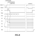
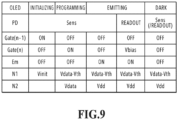
- the control period includes an initialization period in which the pixel unit drive circuit 501 initializes the pixel unit, a write period in which a voltage for driving the pixel unit is precharged, an emission period for the OLED 59, and a read period for reading the PD 58.
- the scan signal Gate (n-1) is at a low level, and the scan signal Gate (n) and the emission signal Em are at a high level.
- the bias voltage VPD at the cathode terminal of the PD 58 is at a high level, and a potential at the anode terminal thereof is close to a low level.
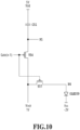
- the low-level scan signal Gate(n-1) turns the reset transistors T54 and T57 on, and the high-level scan signal Gate (n) and emission signal Em turn the other transistors T51 to T53, T55, and T56 off. Therefore, the pixel unit drive circuit 501 takes a circuit configuration as shown in Fig.
- the scan signal Gate(n-1) is at a high level
- the scan signal Gate(n) is at a low level
- the emission signal Em is at a high level.
- the potential at the anode terminal of the PD 58 is at a low level. Therefore, the reset transistors T54 and T57 are turned off, the switching transistors T51 and T56 are turned off, and the compensation transistor T55 and the driving transistor T53 are turned on.
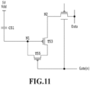
- the scan signal Gate(n) also turns the switching transistor T52 on, and the emission signal Em turns the switching transistors T51 and T56 off, so that the pixel unit drive circuit 501 takes a circuit configuration as shown in Fig. 11 .
- the data signal of the voltage level V data to be applied to the corresponding data line is applied to the source of the driving transistor T53 (Node N2), the voltage of the gate of the driving transistor T53 (Node N1) is stabilized to be V data -V th , where V th is the threshold voltage of the driving transistor T53. Then, electric charges corresponding to the gate voltage V data -V th are stored in the capacitor C51, which completes the precharge operation.
- the scan signal Gate (n) is at a high level, and the emission signal Em goes low after the scan signal Gate(n-1) goes high.
- the potential at the anode terminal of the PD 58 goes low.
- the low-level emission signal Em turns the switching transistors T51 and T56 on
- the high-level scan signal Gate(n-1) turns the reset transistors T54 and T57 off
- the high-level scan signal Gate(n) turns the compensation transistor T55 and the switching transistor T52 off, so that the pixel unit drive circuit 501 has a circuit configuration formed as shown in Fig. 12 .
- the drive current which is generated according to the charge voltage (V data -V th ) corresponding to the data signal input to the gate of the driving transistor T53 is supplied via the transistor T53 to the OLED 59, thus causing the OLED 59 to emit light. That is, the current that does not depend on the threshold voltage of the TFT flows through the OLED 59, so that the OLED 59 emits light.
- the scan signal Gate(n-1) is at a high level.
- the pulse level of the scan signal Gate(n) to be supplied to the bottom gate (second gate) of the switching transistor T52 is adaptively controlled to be a middle level (hereinafter, referred to as "intermediate level V bias ") between the low level and the high level.
- the emission signal Em is at a low level, and the potential at the anode terminal of the PD 58 is almost at a high level.
- the reset transistors T54 and T57 are turned off, and the switching transistors T51 and T56 are turned on by the emission signal Em.
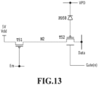
- the pixel unit drive circuit 501 takes a circuit configuration as shown in Fig. 13 , so that a voltage corresponding to the stored initial charges by irradiation of light onto the PD 58 is applied to the top gate. Because an intermediate voltage is applied to the switching transistor T52 by the scan signal Gate(n) at this time, a current according to the voltage at the top gate is supplied to the data line Data from the power supply of the power supply voltage V dd .
- a three-dimensional active pixel sensor (3D-APS) is used.
- a control method in the PD read period (Readout) of the 3D-APS will be described.
- a photosensor is affected by ambient environmental light, which raises the following problem in the case of a highly sensitive photosensor like a 3D-APS.
- a predetermined gate voltage V G_t is applied to the top gate TG of the transistor T52, which is a dual gate transistor, via the PD 58.
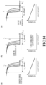
- the gate voltage V G_t of the top gate TG varies according to the amount of light received at the PD 58. At this time, as shown in Fig.
- the drain current I D becomes maximum when the OLED is ON (when the amount of light received at the PD 58 is large), the drain current I D becomes minimum when the OLED is OFF (when the amount of light received at the PD 58 is small), and the gate voltage V G_b (V bias ) of the bottom gate BG is set to a level such that the drain current I D changes between the point of the maximum drain current I D and the point of the minimum drain current I D according to the amount of light received at the PD 58.
- the gate voltage V G_b of the bottom gate BG is adaptively changed according to the intensity of ambient environmental light.
- the gate voltage V G_b (V bias ) is set according to a signal from a photosensor which is implemented separately from the pixel circuit to monitor environmental light. In this manner, the photosensor is not affected by ambient environmental light and can operate as a highly sensitive photosensor.
- the pixel circuit may use 6T1C+APS, or other pixel unit drive circuits may use a dual gate transistor for a switching transistor for switching a data signal applied to a data line, so that the dual gate transistor operates as a readout transistor for reading out a signal from the photosensor as well as an amplification transistor for amplifying a signal.
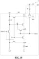
- Fig. 15 shows the configuration of a pixel unit drive circuit according to another embodiment.
- a 7T1C circuit as a pixel circuit is configured with p-type thin film transistors (TFTs).
- the pixel circuit 6 including a combination of a pixel unit drive circuit 601 and a photosensor 602 may be configured with n-type TFTs.
- electrodes of transistors in the pixel unit drive circuit 601 and the photosensor 602 is opposite to that of the 7T1C circuit as shown in Fig. 7 .
- Fig. 16 shows the configuration of a PD reading circuit according to an embodiment of the present invention.
- a signal (V data ) read out from a PD 58 in a pixel circuit 71 is smoothed in a multiplexer (Mux) 72 implemented in the panel of an organic EL display, is then amplified by a front-end amplifier (AFE) 73, and is then input to a sampling circuit (CDS) 74.
- the CDS 74 compares the input signal with a reference signal at a time of no input light to convert the level of the measured signal.
- the signal converted by the CDS 74 is converted by an analog-digital converter (ADC) 75 to a digital signal, which is in turn output.
- ADC analog-digital converter
- the sampling rate in the CDS 74 is changed to lower the signal level by the light intensity according to environmental light. That is, as the intensity of environmental light becomes stronger, on-time of a switch in the CDS 74 is made shorter to narrow the pulse width and the sampling period is made shorter, thereby lowering the signal level.
- the sampling period or the coupling capacitance (C 1b ) in the AFE 73 is changed according to the intensity of environmental light. That is, as in the case of the CDS 74, as the intensity of environmental light becomes stronger, on-time of a switch VSEN EN is made shorter to narrow the pulse width and the sampling period is made shorter, thereby lowering the signal level. By changing a capacitance value of the coupling capacitance (C 1b ), an amplitude gain is made lower, thereby lowering the signal level.
- a column amplifier circuit is used for each data line in the Mux 72, and the sampling period of the column amplifier or the coupling capacitance is changed according to the intensity of environmental light.
- Fig. 17 shows an example of a column amplifier circuit in the PD reading circuit.
- switches CL, FF and FBD go on, a node A becomes a voltage of an offset voltage VOF of the column amplifier circuit in addition to a voltage VC of a power supply.
- a switch SHS goes off, a readout voltage V sig of a signal EL is changed to a reset voltage V rst .
Landscapes
- Engineering & Computer Science (AREA)
- Physics & Mathematics (AREA)
- Computer Hardware Design (AREA)
- General Physics & Mathematics (AREA)
- Theoretical Computer Science (AREA)
- Control Of Indicators Other Than Cathode Ray Tubes (AREA)
- Electroluminescent Light Sources (AREA)
- Control Of El Displays (AREA)
Claims (9)
- Pixelschaltung, die Folgendes beinhaltet: eine organische lichtemittierende Diode (31, 59); einen Kondensator (C11, C51);
einen Schalttransistor (T12, T52), um als Reaktion auf ein an eine Scanleitung angelegtes Scansignal (Gate(n)) auf ein Datensignal mit einem Spannungspegel (Vdata) zu schalten, der an eine entsprechende Datenleitung anzulegen ist; einen Treibertransistor (T13, T53) zum Zuführen eines Treiberstroms zu der organischen lichtemittierenden Diode (31, 59) gemäß einer Ladespannung entsprechend dem Datensignal, das über den Schalttransistor (T12, T52) in den Treibertransistor (T13, T53) eingegeben wird, und wobei die organische lichtemittierende Diode (31, 59) dazu konfiguriert ist, Licht entsprechend dem Treiberstrom zu emittieren; einen zweiten Schalttransistor (T11, T51) zum Zuführen einer Stromversorgungsspannung (Vdd) an den Treibertransistor (T13, T53) als Reaktion auf ein Emissionssignal (Em); einen dritten Schalttransistor (T16, T56) zum Zuführen des über den Treibertransistor (T13, T53) eingegebenen Treiberstroms an die organische lichtemittierende Diode (31, 59) als Reaktion auf das Emissionssignal (Em); und einen Kompensationstransistor (T15, T55) zum Kompensieren einer Schwellenspannung des Treibertransistors (T13, T53), wobei die Pixelschaltung ferner Folgendes umfasst:einen Photosensor (PD 58), der einen Kathodenanschluss aufweist, an welchen eine Hochspannung angelegt wird,wobei der Schalttransistor (T12, T52) ein Dual-Gate-Transistor ist, der ein erstes Gate aufweist, das mit einem Anodenanschluss des Photosensors verbunden ist, und der ein zweites Gate aufweist, das mit einem Gate des Kompensationstransistors verbunden ist, und wobei der Schalttransistor (T12, T52) als Auslesetransistor fungiert, welcher ein Signal aus dem Photosensor (PD 58) ausliest;wobei der Schalttransistor (T12, T52) eine Source, an welcher das Datensignal des an die entsprechende Datenleitung angelegten Spannungspegels (Vdata) angelegt wird, und einen Drain aufweist, der mit einer Source des Treibertransistors (T13, T53) verbunden ist;wobei der Treibertransistor (T13, T53) ein Gate, das mit einem Anschluss des Kondensators (C11, C51) verbunden ist, und ein Drain aufweist, der über den dritten Schalttransistor (T16, T56) mit einem Anodenanschluss der organischen lichtemittierenden Diode (31, 59) verbunden ist;wobei der Kompensationstransistor (T15, T55) einen Drain, der mit dem Gate des Treibertransistors (T13, T53) verbunden ist, eine Source, die mit dem Drain des Treibertransistors (T13, T53) verbunden ist, und ein Gate aufweist, an welches das Scansignal (Gate(n)) angelegt wird;wobei der zweite Schalttransistor (T11, T51) ein Gate, an welches das Emissionssignal (Em) angelegt wird, eine Source, an welche die Stromversorgungsspannung (Vdd) angelegt wird, und einen Drain aufweist, der mit der Source des Treibertransistors (T13, T53) verbunden ist;wobei der dritte Schalttransistor (T16, T56) ein Gate, an welches das Emissionssignal (Em) angelegt wird, eine Source, die mit dem Drain des Treibertransistors (T13, T53) verbunden ist, und einen Drain aufweist, der mit dem Anodenanschluss der organischen lichtemittierenden Diode (31, 59) verbunden ist;wobei die Stromversorgungsspannung (Vdd) mit hohem Pegel dem anderen Anschluss des Kondensators (C11, C51) zugeführt wird; undwobei die organische lichtemittierende Diode (31) einen Kathodenanschluss aufweist, der mit einer Stromversorgungsspannung (Vss) verbunden ist; undwobei ein Scansignal zum Einschalten des Dual-Gate-Transistors an das zweite Gate angelegt wird, um das an die Datenleitung angelegte Datensignal aufzuladen, und ein adaptiv gesteuertes Scansignal an das zweite Gate angelegt wird, um ein Signal aus dem Photosensor aus der Datenleitung auszulesen. - Pixelschaltung nach Anspruch 1, wobei das adaptiv gesteuerte Scansignal eine Spannung mit einem Pegel zwischen einem hohen Pegel und einem niedrigen Pegel ist, wodurch eine Spannung des zweiten Gates gemäß den von dem Photosensor gespeicherten Ladungen variiert wird, und ein Strom gemäß einer an das erste Gate und das zweite Gate angelegten Spannung durch die Datenleitung fließt.
- Pixelschaltung nach Anspruch 1, wobei das adaptiv gesteuerte Scansignal gemäß einer Intensität von Umgebungslicht gesteuert wird.
- Anzeigevorrichtung, umfassend:
eine Vielzahl von Pixeleinheiten und eine Abdeckplatte, wobei sich die Vielzahl von Pixeleinheiten insgesamt auf derselben Seite der Abdeckplatte befindet, wobei jede Pixeleinheit eine Pixelschaltung nach einem der Ansprüche 1 bis 3 beinhaltet. - Anzeigevorrichtung nach Anspruch 4, ferner umfassend:
eine Verschlussfunktion zum Durchführen einer Pegelumwandlung an einem Signal aus dem Photosensor, der aus der Datenleitung ausgelesen wird. - Pixelsteuerungsverfahren für eine Pixelschaltung nach einem der Ansprüche 1 bis 3, wobei das Verfahren Folgendes umfasst:Bewirken, dass der Dual-Gate-Transistor als ein Schalter zum Schalten des Datensignals fungiert; undBewirken, dass der Dual-Gate-Transistor als ein Verstärker des Photosensors fungiert, um ein Signal aus dem Photosensor aus der Datenleitung auszulesen.
- Verfahren nach Anspruch 6, wobei das Bewirken, dass der Dual-Gate-Transistor als ein Schalter zum Schalten des Datensignals fungiert, ein Scansignal zum Einschalten des Dual-Gate-Transistors an das zweite Gate anlegt, um das an die Datenleitung angelegte Datensignal zu laden.
- Verfahren nach Anspruch 6 oder 7, wobei das Auslesen eines Signals aus dem Photosensor aus der Datenleitung eine Spannung mit einem Pegel zwischen einem hohen Pegel und einem niedrigen Pegel an das zweite Gate anlegt, wodurch eine Spannung des zweiten Gates gemäß den von dem Photosensor gespeicherten Ladungen variiert und ein Strom gemäß einer an das erste Gate angelegten Spannung durch die Datenleitung fließt.
- Verfahren nach Anspruch 6 oder 7, wobei das Auslesen eines Signals aus dem Photosensor aus der Datenleitung ein Scansignal, das adaptiv gemäß einer Intensität des Umgebungslichts gesteuert wird, an das zweite Gate anlegt.
Applications Claiming Priority (1)
| Application Number | Priority Date | Filing Date | Title |
|---|---|---|---|
| PCT/CN2019/089595 WO2020237649A1 (en) | 2019-05-31 | 2019-05-31 | Pixel circuit and pixel control method |
Publications (3)
| Publication Number | Publication Date |
|---|---|
| EP3970135A1 EP3970135A1 (de) | 2022-03-23 |
| EP3970135A4 EP3970135A4 (de) | 2022-04-13 |
| EP3970135B1 true EP3970135B1 (de) | 2024-11-06 |
Family
ID=73552708
Family Applications (1)
| Application Number | Title | Priority Date | Filing Date |
|---|---|---|---|
| EP19931075.6A Active EP3970135B1 (de) | 2019-05-31 | 2019-05-31 | Pixelschaltung und pixelsteuerungsverfahren |
Country Status (4)
| Country | Link |
|---|---|
| US (1) | US12067936B2 (de) |
| EP (1) | EP3970135B1 (de) |
| CN (1) | CN113892133B (de) |
| WO (1) | WO2020237649A1 (de) |
Families Citing this family (9)
| Publication number | Priority date | Publication date | Assignee | Title |
|---|---|---|---|---|
| CN114397975B (zh) * | 2022-01-24 | 2024-04-09 | 武汉天马微电子有限公司 | 显示面板及其驱动方法和显示装置 |
| TWI802386B (zh) * | 2022-04-25 | 2023-05-11 | 大陸商北京歐錸德微電子技術有限公司 | 畫素電路、oled顯示裝置及資訊處理裝置 |
| CN115379139B (zh) * | 2022-08-16 | 2025-01-28 | 成都微光集电科技有限公司 | 图像传感器读出方法 |
| CN115762411B (zh) * | 2022-12-15 | 2026-02-17 | 云谷(固安)科技有限公司 | 栅极驱动电路和显示面板 |
| US12437715B2 (en) * | 2023-03-31 | 2025-10-07 | Chongqing Boe Display Technology Co., Ltd. | Display apparatus, pixel circuit, and method for driving pixel circuit |
| CN116412842A (zh) | 2023-04-14 | 2023-07-11 | 上海天马微电子有限公司 | 传感检测电路及其检测方法、传感检测芯片及显示面板 |
| CN117437878A (zh) * | 2023-11-24 | 2024-01-23 | 合肥维信诺科技有限公司 | 显示电路、显示面板与显示装置 |
| KR20250148025A (ko) * | 2024-04-04 | 2025-10-14 | 삼성디스플레이 주식회사 | 표시 장치 및 이의 구동 방법 |
| KR20250174159A (ko) * | 2024-06-04 | 2025-12-12 | 삼성디스플레이 주식회사 | 픽셀 회로 및 이를 포함하는 표시 장치 |
Family Cites Families (28)
| Publication number | Priority date | Publication date | Assignee | Title |
|---|---|---|---|---|
| GB0014962D0 (en) * | 2000-06-20 | 2000-08-09 | Koninkl Philips Electronics Nv | Matrix array display devices with light sensing elements and associated storage capacitors |
| US20050030264A1 (en) * | 2001-09-07 | 2005-02-10 | Hitoshi Tsuge | El display, el display driving circuit and image display |
| GB2381644A (en) * | 2001-10-31 | 2003-05-07 | Cambridge Display Tech Ltd | Display drivers |
| KR100560780B1 (ko) | 2003-07-07 | 2006-03-13 | 삼성에스디아이 주식회사 | 유기전계 발광표시장치의 화소회로 및 그의 구동방법 |
| GB0424112D0 (en) * | 2004-10-29 | 2004-12-01 | Koninkl Philips Electronics Nv | Active matrix display devices |
| KR100627417B1 (ko) * | 2005-08-26 | 2006-09-22 | 삼성에스디아이 주식회사 | 유기 발광 표시 장치 및 그 구동 방법 |
| EP1840971A1 (de) * | 2006-03-31 | 2007-10-03 | Toppoly Optoelectronics Corp. | Organische elektrolumineszente Vorrichtung und Methode zu ihrer Herstellung |
| CN103354077B (zh) * | 2013-05-31 | 2017-02-08 | 上海和辉光电有限公司 | 一种像素驱动电路及显示面板 |
| CN103295525B (zh) * | 2013-05-31 | 2015-09-30 | 京东方科技集团股份有限公司 | 像素电路及其驱动方法、有机发光显示面板及显示装置 |
| CN103354079B (zh) * | 2013-06-26 | 2015-04-08 | 京东方科技集团股份有限公司 | 一种有源矩阵有机发光二极管像素单元电路以及显示面板 |
| CN103762251B (zh) | 2014-01-22 | 2016-03-30 | 中山大学 | 一种双栅极光电薄膜晶体管、像素电路及像素阵列 |
| CN104573648B (zh) | 2014-12-31 | 2018-06-26 | 广东顺德中山大学卡内基梅隆大学国际联合研究院 | 一种触控显示屏驱动及指纹图像采集方法 |
| KR102287353B1 (ko) * | 2015-01-27 | 2021-08-06 | 삼성디스플레이 주식회사 | 표시 장치 및 그 리페어 방법 |
| US10585506B2 (en) * | 2015-07-30 | 2020-03-10 | Semiconductor Energy Laboratory Co., Ltd. | Display device with high visibility regardless of illuminance of external light |
| KR102516592B1 (ko) * | 2015-08-24 | 2023-03-31 | 삼성디스플레이 주식회사 | 유기 발광 표시 장치 |
| CN205262967U (zh) | 2015-11-02 | 2016-05-25 | 广东顺德中山大学卡内基梅隆大学国际联合研究院 | 一种数字pcr分析仪 |
| WO2017184132A1 (en) | 2016-04-20 | 2017-10-26 | Entit Software Llc | Replacing a subset of digits in a sequence |
| CN105870174A (zh) | 2016-05-03 | 2016-08-17 | 广东顺德中山大学卡内基梅隆大学国际联合研究院 | 双栅极光电薄膜晶体管的光栅极复合膜结构及薄膜晶体管 |
| US10431154B2 (en) * | 2016-06-15 | 2019-10-01 | Apple Inc. | Light-emitting diode display with reduced leakage |
| CN106295540B (zh) * | 2016-08-02 | 2019-08-13 | 广东顺德中山大学卡内基梅隆大学国际联合研究院 | 采用单一器件实现显示驱动和指纹图像采集的方法 |
| WO2018023424A1 (zh) | 2016-08-02 | 2018-02-08 | 广东顺德中山大学卡内基梅隆大学国际联合研究院 | 采用单一器件实现显示驱动和指纹图像采集的方法 |
| KR102730433B1 (ko) * | 2016-09-02 | 2024-11-14 | 삼성디스플레이 주식회사 | 유기 발광 표시 장치 |
| CN106546743B (zh) | 2016-11-04 | 2018-09-04 | 中山大学 | 一种羊水栓塞血清学指标的实时监测系统和监测方法 |
| CN106782272B (zh) * | 2017-01-18 | 2021-01-15 | 京东方科技集团股份有限公司 | 像素电路及其驱动方法、显示装置 |
| CN107255710B (zh) | 2017-06-01 | 2019-07-09 | 广东顺德中山大学卡内基梅隆大学国际联合研究院 | 多通道微流控荧光检测装置和方法 |
| CN107301844A (zh) * | 2017-07-19 | 2017-10-27 | 深圳市华星光电半导体显示技术有限公司 | Oled像素驱动电路 |
| CN107358916B (zh) * | 2017-08-15 | 2020-01-14 | 上海天马有机发光显示技术有限公司 | 像素电路、其驱动方法、电致发光显示面板及显示装置 |
| CN108735782B (zh) * | 2018-04-19 | 2021-10-19 | 佛山市顺德区中山大学研究院 | 一种基于oled的光电传感器的垂直集成结构 |
-
2019
- 2019-05-31 CN CN201980096947.8A patent/CN113892133B/zh active Active
- 2019-05-31 WO PCT/CN2019/089595 patent/WO2020237649A1/en not_active Ceased
- 2019-05-31 EP EP19931075.6A patent/EP3970135B1/de active Active
-
2021
- 2021-11-30 US US17/538,571 patent/US12067936B2/en active Active
Also Published As
| Publication number | Publication date |
|---|---|
| CN113892133B (zh) | 2023-03-28 |
| EP3970135A1 (de) | 2022-03-23 |
| WO2020237649A1 (en) | 2020-12-03 |
| US20220084466A1 (en) | 2022-03-17 |
| CN113892133A (zh) | 2022-01-04 |
| EP3970135A4 (de) | 2022-04-13 |
| US12067936B2 (en) | 2024-08-20 |
Similar Documents
| Publication | Publication Date | Title |
|---|---|---|
| US12067936B2 (en) | Pixel circuit and pixel control method | |
| US11108980B2 (en) | Semiconductor devices with single-photon avalanche diode pixels | |
| US10818226B2 (en) | Pixel circuit, method for driving the same, and display apparatus | |
| EP2178293B1 (de) | Aktivpixelsensorschaltung | |
| JP4055722B2 (ja) | アクティブマトリクス型有機el表示装置 | |
| US8217328B2 (en) | Low noise pixel readout circuit with high conversion gain | |
| US8552354B2 (en) | Solid-state image pickup element having a control circuit for controlling the operation period of a transfer circuit and method for controlling the same | |
| US8174466B2 (en) | Display device and driving method thereof | |
| US9106851B2 (en) | Single-exposure high dynamic range CMOS image sensor pixel with internal charge amplifier | |
| US20220036825A1 (en) | Pixel circuit and pixel control method | |
| US11348517B2 (en) | Pixel circuit, driving method thereof and display device | |
| US20240127756A1 (en) | Pixel Driving Circuit, Pixel Driving Method, Display Panel and Display Device | |
| US20160360132A1 (en) | Imaging device including pixels | |
| CN114627788B (zh) | 光电传感像素补偿电路、驱动方法及显示装置 | |
| US11081055B2 (en) | Active matrix-based electronic apparatus including a light emitting device that may be non-foward biased to sense light, and method of driving the same | |
| US20120223925A1 (en) | Photodetection circuit, photodetection method, display panel, and display | |
| US10447954B2 (en) | Unit pixel apparatus and operation method thereof | |
| US20240014242A1 (en) | Spad-based devices with transistor stacking | |
| US11849237B1 (en) | Pixel circuit adopting optically sensitive material with suppressed dark current | |
| KR20200098024A (ko) | 이미지 센서의 펄스 생성기 및 이의 구동 방법 | |
| KR100448986B1 (ko) | 단일 트랜지스터형 이미지 셀 | |
| KR100694463B1 (ko) | 보정회로 및 이를 구비한 이미지 센서 |
Legal Events
| Date | Code | Title | Description |
|---|---|---|---|
| STAA | Information on the status of an ep patent application or granted ep patent |
Free format text: STATUS: THE INTERNATIONAL PUBLICATION HAS BEEN MADE |
|
| PUAI | Public reference made under article 153(3) epc to a published international application that has entered the european phase |
Free format text: ORIGINAL CODE: 0009012 |
|
| STAA | Information on the status of an ep patent application or granted ep patent |
Free format text: STATUS: REQUEST FOR EXAMINATION WAS MADE |
|
| 17P | Request for examination filed |
Effective date: 20211216 |
|
| AK | Designated contracting states |
Kind code of ref document: A1 Designated state(s): AL AT BE BG CH CY CZ DE DK EE ES FI FR GB GR HR HU IE IS IT LI LT LU LV MC MK MT NL NO PL PT RO RS SE SI SK SM TR |
|
| A4 | Supplementary search report drawn up and despatched |
Effective date: 20220311 |
|
| RIC1 | Information provided on ipc code assigned before grant |
Ipc: G09G 3/32 20160101AFI20220305BHEP |
|
| DAV | Request for validation of the european patent (deleted) | ||
| DAX | Request for extension of the european patent (deleted) | ||
| GRAP | Despatch of communication of intention to grant a patent |
Free format text: ORIGINAL CODE: EPIDOSNIGR1 |
|
| STAA | Information on the status of an ep patent application or granted ep patent |
Free format text: STATUS: GRANT OF PATENT IS INTENDED |
|
| INTG | Intention to grant announced |
Effective date: 20240207 |
|
| GRAJ | Information related to disapproval of communication of intention to grant by the applicant or resumption of examination proceedings by the epo deleted |
Free format text: ORIGINAL CODE: EPIDOSDIGR1 |
|
| STAA | Information on the status of an ep patent application or granted ep patent |
Free format text: STATUS: REQUEST FOR EXAMINATION WAS MADE |
|
| GRAP | Despatch of communication of intention to grant a patent |
Free format text: ORIGINAL CODE: EPIDOSNIGR1 |
|
| STAA | Information on the status of an ep patent application or granted ep patent |
Free format text: STATUS: GRANT OF PATENT IS INTENDED |
|
| INTC | Intention to grant announced (deleted) | ||
| INTG | Intention to grant announced |
Effective date: 20240625 |
|
| GRAS | Grant fee paid |
Free format text: ORIGINAL CODE: EPIDOSNIGR3 |
|
| GRAA | (expected) grant |
Free format text: ORIGINAL CODE: 0009210 |
|
| STAA | Information on the status of an ep patent application or granted ep patent |
Free format text: STATUS: THE PATENT HAS BEEN GRANTED |
|
| AK | Designated contracting states |
Kind code of ref document: B1 Designated state(s): AL AT BE BG CH CY CZ DE DK EE ES FI FR GB GR HR HU IE IS IT LI LT LU LV MC MK MT NL NO PL PT RO RS SE SI SK SM TR |
|
| REG | Reference to a national code |
Ref country code: GB Ref legal event code: FG4D |
|
| REG | Reference to a national code |
Ref country code: CH Ref legal event code: EP |
|
| REG | Reference to a national code |
Ref country code: DE Ref legal event code: R096 Ref document number: 602019061772 Country of ref document: DE |
|
| REG | Reference to a national code |
Ref country code: IE Ref legal event code: FG4D |
|
| REG | Reference to a national code |
Ref country code: LT Ref legal event code: MG9D |
|
| REG | Reference to a national code |
Ref country code: NL Ref legal event code: MP Effective date: 20241106 |
|
| PG25 | Lapsed in a contracting state [announced via postgrant information from national office to epo] |
Ref country code: PT Free format text: LAPSE BECAUSE OF FAILURE TO SUBMIT A TRANSLATION OF THE DESCRIPTION OR TO PAY THE FEE WITHIN THE PRESCRIBED TIME-LIMIT Effective date: 20250306 Ref country code: HR Free format text: LAPSE BECAUSE OF FAILURE TO SUBMIT A TRANSLATION OF THE DESCRIPTION OR TO PAY THE FEE WITHIN THE PRESCRIBED TIME-LIMIT Effective date: 20241106 Ref country code: IS Free format text: LAPSE BECAUSE OF FAILURE TO SUBMIT A TRANSLATION OF THE DESCRIPTION OR TO PAY THE FEE WITHIN THE PRESCRIBED TIME-LIMIT Effective date: 20250306 |
|
| PG25 | Lapsed in a contracting state [announced via postgrant information from national office to epo] |
Ref country code: NL Free format text: LAPSE BECAUSE OF FAILURE TO SUBMIT A TRANSLATION OF THE DESCRIPTION OR TO PAY THE FEE WITHIN THE PRESCRIBED TIME-LIMIT Effective date: 20241106 Ref country code: FI Free format text: LAPSE BECAUSE OF FAILURE TO SUBMIT A TRANSLATION OF THE DESCRIPTION OR TO PAY THE FEE WITHIN THE PRESCRIBED TIME-LIMIT Effective date: 20241106 |
|
| REG | Reference to a national code |
Ref country code: AT Ref legal event code: MK05 Ref document number: 1740285 Country of ref document: AT Kind code of ref document: T Effective date: 20241106 |
|
| PG25 | Lapsed in a contracting state [announced via postgrant information from national office to epo] |
Ref country code: BG Free format text: LAPSE BECAUSE OF FAILURE TO SUBMIT A TRANSLATION OF THE DESCRIPTION OR TO PAY THE FEE WITHIN THE PRESCRIBED TIME-LIMIT Effective date: 20241106 |
|
| PG25 | Lapsed in a contracting state [announced via postgrant information from national office to epo] |
Ref country code: ES Free format text: LAPSE BECAUSE OF FAILURE TO SUBMIT A TRANSLATION OF THE DESCRIPTION OR TO PAY THE FEE WITHIN THE PRESCRIBED TIME-LIMIT Effective date: 20241106 |
|
| PG25 | Lapsed in a contracting state [announced via postgrant information from national office to epo] |
Ref country code: NO Free format text: LAPSE BECAUSE OF FAILURE TO SUBMIT A TRANSLATION OF THE DESCRIPTION OR TO PAY THE FEE WITHIN THE PRESCRIBED TIME-LIMIT Effective date: 20250206 |
|
| PG25 | Lapsed in a contracting state [announced via postgrant information from national office to epo] |
Ref country code: LV Free format text: LAPSE BECAUSE OF FAILURE TO SUBMIT A TRANSLATION OF THE DESCRIPTION OR TO PAY THE FEE WITHIN THE PRESCRIBED TIME-LIMIT Effective date: 20241106 Ref country code: GR Free format text: LAPSE BECAUSE OF FAILURE TO SUBMIT A TRANSLATION OF THE DESCRIPTION OR TO PAY THE FEE WITHIN THE PRESCRIBED TIME-LIMIT Effective date: 20250207 Ref country code: AT Free format text: LAPSE BECAUSE OF FAILURE TO SUBMIT A TRANSLATION OF THE DESCRIPTION OR TO PAY THE FEE WITHIN THE PRESCRIBED TIME-LIMIT Effective date: 20241106 |
|
| PG25 | Lapsed in a contracting state [announced via postgrant information from national office to epo] |
Ref country code: PL Free format text: LAPSE BECAUSE OF FAILURE TO SUBMIT A TRANSLATION OF THE DESCRIPTION OR TO PAY THE FEE WITHIN THE PRESCRIBED TIME-LIMIT Effective date: 20241106 |
|
| PG25 | Lapsed in a contracting state [announced via postgrant information from national office to epo] |
Ref country code: RS Free format text: LAPSE BECAUSE OF FAILURE TO SUBMIT A TRANSLATION OF THE DESCRIPTION OR TO PAY THE FEE WITHIN THE PRESCRIBED TIME-LIMIT Effective date: 20250206 |
|
| PG25 | Lapsed in a contracting state [announced via postgrant information from national office to epo] |
Ref country code: SM Free format text: LAPSE BECAUSE OF FAILURE TO SUBMIT A TRANSLATION OF THE DESCRIPTION OR TO PAY THE FEE WITHIN THE PRESCRIBED TIME-LIMIT Effective date: 20241106 |
|
| PGFP | Annual fee paid to national office [announced via postgrant information from national office to epo] |
Ref country code: DE Payment date: 20250402 Year of fee payment: 7 |
|
| PG25 | Lapsed in a contracting state [announced via postgrant information from national office to epo] |
Ref country code: DK Free format text: LAPSE BECAUSE OF FAILURE TO SUBMIT A TRANSLATION OF THE DESCRIPTION OR TO PAY THE FEE WITHIN THE PRESCRIBED TIME-LIMIT Effective date: 20241106 |
|
| PGFP | Annual fee paid to national office [announced via postgrant information from national office to epo] |
Ref country code: GB Payment date: 20250401 Year of fee payment: 7 |
|
| PG25 | Lapsed in a contracting state [announced via postgrant information from national office to epo] |
Ref country code: EE Free format text: LAPSE BECAUSE OF FAILURE TO SUBMIT A TRANSLATION OF THE DESCRIPTION OR TO PAY THE FEE WITHIN THE PRESCRIBED TIME-LIMIT Effective date: 20241106 |
|
| PG25 | Lapsed in a contracting state [announced via postgrant information from national office to epo] |
Ref country code: RO Free format text: LAPSE BECAUSE OF FAILURE TO SUBMIT A TRANSLATION OF THE DESCRIPTION OR TO PAY THE FEE WITHIN THE PRESCRIBED TIME-LIMIT Effective date: 20241106 |
|
| PG25 | Lapsed in a contracting state [announced via postgrant information from national office to epo] |
Ref country code: SK Free format text: LAPSE BECAUSE OF FAILURE TO SUBMIT A TRANSLATION OF THE DESCRIPTION OR TO PAY THE FEE WITHIN THE PRESCRIBED TIME-LIMIT Effective date: 20241106 |
|
| PG25 | Lapsed in a contracting state [announced via postgrant information from national office to epo] |
Ref country code: CZ Free format text: LAPSE BECAUSE OF FAILURE TO SUBMIT A TRANSLATION OF THE DESCRIPTION OR TO PAY THE FEE WITHIN THE PRESCRIBED TIME-LIMIT Effective date: 20241106 |
|
| PG25 | Lapsed in a contracting state [announced via postgrant information from national office to epo] |
Ref country code: IT Free format text: LAPSE BECAUSE OF FAILURE TO SUBMIT A TRANSLATION OF THE DESCRIPTION OR TO PAY THE FEE WITHIN THE PRESCRIBED TIME-LIMIT Effective date: 20241106 |
|
| REG | Reference to a national code |
Ref country code: DE Ref legal event code: R097 Ref document number: 602019061772 Country of ref document: DE |
|
| PG25 | Lapsed in a contracting state [announced via postgrant information from national office to epo] |
Ref country code: SE Free format text: LAPSE BECAUSE OF FAILURE TO SUBMIT A TRANSLATION OF THE DESCRIPTION OR TO PAY THE FEE WITHIN THE PRESCRIBED TIME-LIMIT Effective date: 20241106 |
|
| PLBE | No opposition filed within time limit |
Free format text: ORIGINAL CODE: 0009261 |
|
| STAA | Information on the status of an ep patent application or granted ep patent |
Free format text: STATUS: NO OPPOSITION FILED WITHIN TIME LIMIT |
|
| 26N | No opposition filed |
Effective date: 20250807 |
|
| REG | Reference to a national code |
Ref country code: CH Ref legal event code: H13 Free format text: ST27 STATUS EVENT CODE: U-0-0-H10-H13 (AS PROVIDED BY THE NATIONAL OFFICE) Effective date: 20251223 |
|
| PG25 | Lapsed in a contracting state [announced via postgrant information from national office to epo] |
Ref country code: LU Free format text: LAPSE BECAUSE OF NON-PAYMENT OF DUE FEES Effective date: 20250531 |
|
| PG25 | Lapsed in a contracting state [announced via postgrant information from national office to epo] |
Ref country code: CH Free format text: LAPSE BECAUSE OF NON-PAYMENT OF DUE FEES Effective date: 20250531 |
|
| REG | Reference to a national code |
Ref country code: BE Ref legal event code: MM Effective date: 20250531 |
|
| PG25 | Lapsed in a contracting state [announced via postgrant information from national office to epo] |
Ref country code: MC Free format text: LAPSE BECAUSE OF FAILURE TO SUBMIT A TRANSLATION OF THE DESCRIPTION OR TO PAY THE FEE WITHIN THE PRESCRIBED TIME-LIMIT Effective date: 20241106 |
|
| PG25 | Lapsed in a contracting state [announced via postgrant information from national office to epo] |
Ref country code: IE Free format text: LAPSE BECAUSE OF NON-PAYMENT OF DUE FEES Effective date: 20250531 |
|
| PG25 | Lapsed in a contracting state [announced via postgrant information from national office to epo] |
Ref country code: BE Free format text: LAPSE BECAUSE OF NON-PAYMENT OF DUE FEES Effective date: 20250531 |
|
| PG25 | Lapsed in a contracting state [announced via postgrant information from national office to epo] |
Ref country code: FR Free format text: LAPSE BECAUSE OF NON-PAYMENT OF DUE FEES Effective date: 20250531 |