EP3968518A1 - Dc-dc voltage converter with floating rail generation for cascode transistor biasing - Google Patents
Dc-dc voltage converter with floating rail generation for cascode transistor biasing Download PDFInfo
- Publication number
- EP3968518A1 EP3968518A1 EP21192626.6A EP21192626A EP3968518A1 EP 3968518 A1 EP3968518 A1 EP 3968518A1 EP 21192626 A EP21192626 A EP 21192626A EP 3968518 A1 EP3968518 A1 EP 3968518A1
- Authority
- EP
- European Patent Office
- Prior art keywords
- voltage
- power supply
- vdd
- circuit
- supply voltage
- Prior art date
- Legal status (The legal status is an assumption and is not a legal conclusion. Google has not performed a legal analysis and makes no representation as to the accuracy of the status listed.)
- Granted
Links
Images



Classifications
-
- H—ELECTRICITY
- H02—GENERATION; CONVERSION OR DISTRIBUTION OF ELECTRIC POWER
- H02M—APPARATUS FOR CONVERSION BETWEEN AC AND AC, BETWEEN AC AND DC, OR BETWEEN DC AND DC, AND FOR USE WITH MAINS OR SIMILAR POWER SUPPLY SYSTEMS; CONVERSION OF DC OR AC INPUT POWER INTO SURGE OUTPUT POWER; CONTROL OR REGULATION THEREOF
- H02M3/00—Conversion of DC power input into DC power output
- H02M3/02—Conversion of DC power input into DC power output without intermediate conversion into AC
- H02M3/04—Conversion of DC power input into DC power output without intermediate conversion into AC by static converters
- H02M3/10—Conversion of DC power input into DC power output without intermediate conversion into AC by static converters using discharge tubes with control electrode or semiconductor devices with control electrode
- H02M3/145—Conversion of DC power input into DC power output without intermediate conversion into AC by static converters using discharge tubes with control electrode or semiconductor devices with control electrode using devices of a triode or transistor type requiring continuous application of a control signal
- H02M3/155—Conversion of DC power input into DC power output without intermediate conversion into AC by static converters using discharge tubes with control electrode or semiconductor devices with control electrode using devices of a triode or transistor type requiring continuous application of a control signal using semiconductor devices only
- H02M3/156—Conversion of DC power input into DC power output without intermediate conversion into AC by static converters using discharge tubes with control electrode or semiconductor devices with control electrode using devices of a triode or transistor type requiring continuous application of a control signal using semiconductor devices only with automatic control of output voltage or current, e.g. switching regulators
- H02M3/158—Conversion of DC power input into DC power output without intermediate conversion into AC by static converters using discharge tubes with control electrode or semiconductor devices with control electrode using devices of a triode or transistor type requiring continuous application of a control signal using semiconductor devices only with automatic control of output voltage or current, e.g. switching regulators including plural semiconductor devices as final control devices for a single load
- H02M3/1584—Conversion of DC power input into DC power output without intermediate conversion into AC by static converters using discharge tubes with control electrode or semiconductor devices with control electrode using devices of a triode or transistor type requiring continuous application of a control signal using semiconductor devices only with automatic control of output voltage or current, e.g. switching regulators including plural semiconductor devices as final control devices for a single load with a plurality of power processing stages connected in parallel
-
- H—ELECTRICITY
- H02—GENERATION; CONVERSION OR DISTRIBUTION OF ELECTRIC POWER
- H02M—APPARATUS FOR CONVERSION BETWEEN AC AND AC, BETWEEN AC AND DC, OR BETWEEN DC AND DC, AND FOR USE WITH MAINS OR SIMILAR POWER SUPPLY SYSTEMS; CONVERSION OF DC OR AC INPUT POWER INTO SURGE OUTPUT POWER; CONTROL OR REGULATION THEREOF
- H02M1/00—Details of apparatus for conversion
-
- H—ELECTRICITY
- H02—GENERATION; CONVERSION OR DISTRIBUTION OF ELECTRIC POWER
- H02M—APPARATUS FOR CONVERSION BETWEEN AC AND AC, BETWEEN AC AND DC, OR BETWEEN DC AND DC, AND FOR USE WITH MAINS OR SIMILAR POWER SUPPLY SYSTEMS; CONVERSION OF DC OR AC INPUT POWER INTO SURGE OUTPUT POWER; CONTROL OR REGULATION THEREOF
- H02M1/00—Details of apparatus for conversion
- H02M1/08—Circuits specially adapted for the generation of control voltages for semiconductor devices incorporated in static converters
- H02M1/088—Circuits specially adapted for the generation of control voltages for semiconductor devices incorporated in static converters for the simultaneous control of series or parallel connected semiconductor devices
-
- H—ELECTRICITY
- H03—ELECTRONIC CIRCUITRY
- H03K—PULSE TECHNIQUE
- H03K17/00—Electronic switching or gating, i.e. not by contact-making and –breaking
- H03K17/06—Modifications for ensuring a fully conducting state
- H03K17/063—Modifications for ensuring a fully conducting state in field-effect transistor switches
-
- H—ELECTRICITY
- H03—ELECTRONIC CIRCUITRY
- H03K—PULSE TECHNIQUE
- H03K17/00—Electronic switching or gating, i.e. not by contact-making and –breaking
- H03K17/08—Modifications for protecting switching circuit against overcurrent or overvoltage
- H03K17/081—Modifications for protecting switching circuit against overcurrent or overvoltage without feedback from the output circuit to the control circuit
- H03K17/0812—Modifications for protecting switching circuit against overcurrent or overvoltage without feedback from the output circuit to the control circuit by measures taken in the control circuit
- H03K17/08122—Modifications for protecting switching circuit against overcurrent or overvoltage without feedback from the output circuit to the control circuit by measures taken in the control circuit in field-effect transistor switches
-
- H—ELECTRICITY
- H03—ELECTRONIC CIRCUITRY
- H03K—PULSE TECHNIQUE
- H03K17/00—Electronic switching or gating, i.e. not by contact-making and –breaking
- H03K17/51—Electronic switching or gating, i.e. not by contact-making and –breaking characterised by the components used
- H03K17/56—Electronic switching or gating, i.e. not by contact-making and –breaking characterised by the components used by the use, as active elements, of semiconductor devices
- H03K17/687—Electronic switching or gating, i.e. not by contact-making and –breaking characterised by the components used by the use, as active elements, of semiconductor devices the devices being field-effect transistors
- H03K17/6871—Electronic switching or gating, i.e. not by contact-making and –breaking characterised by the components used by the use, as active elements, of semiconductor devices the devices being field-effect transistors the output circuit comprising more than one controlled field-effect transistor
- H03K17/6872—Electronic switching or gating, i.e. not by contact-making and –breaking characterised by the components used by the use, as active elements, of semiconductor devices the devices being field-effect transistors the output circuit comprising more than one controlled field-effect transistor using complementary field-effect transistors
-
- H—ELECTRICITY
- H02—GENERATION; CONVERSION OR DISTRIBUTION OF ELECTRIC POWER
- H02M—APPARATUS FOR CONVERSION BETWEEN AC AND AC, BETWEEN AC AND DC, OR BETWEEN DC AND DC, AND FOR USE WITH MAINS OR SIMILAR POWER SUPPLY SYSTEMS; CONVERSION OF DC OR AC INPUT POWER INTO SURGE OUTPUT POWER; CONTROL OR REGULATION THEREOF
- H02M1/00—Details of apparatus for conversion
- H02M1/0003—Details of control, feedback or regulation circuits
- H02M1/0006—Arrangements for supplying an adequate voltage to the control circuit of converters
-
- H—ELECTRICITY
- H02—GENERATION; CONVERSION OR DISTRIBUTION OF ELECTRIC POWER
- H02M—APPARATUS FOR CONVERSION BETWEEN AC AND AC, BETWEEN AC AND DC, OR BETWEEN DC AND DC, AND FOR USE WITH MAINS OR SIMILAR POWER SUPPLY SYSTEMS; CONVERSION OF DC OR AC INPUT POWER INTO SURGE OUTPUT POWER; CONTROL OR REGULATION THEREOF
- H02M3/00—Conversion of DC power input into DC power output
- H02M3/02—Conversion of DC power input into DC power output without intermediate conversion into AC
- H02M3/04—Conversion of DC power input into DC power output without intermediate conversion into AC by static converters
- H02M3/10—Conversion of DC power input into DC power output without intermediate conversion into AC by static converters using discharge tubes with control electrode or semiconductor devices with control electrode
- H02M3/145—Conversion of DC power input into DC power output without intermediate conversion into AC by static converters using discharge tubes with control electrode or semiconductor devices with control electrode using devices of a triode or transistor type requiring continuous application of a control signal
- H02M3/155—Conversion of DC power input into DC power output without intermediate conversion into AC by static converters using discharge tubes with control electrode or semiconductor devices with control electrode using devices of a triode or transistor type requiring continuous application of a control signal using semiconductor devices only
- H02M3/156—Conversion of DC power input into DC power output without intermediate conversion into AC by static converters using discharge tubes with control electrode or semiconductor devices with control electrode using devices of a triode or transistor type requiring continuous application of a control signal using semiconductor devices only with automatic control of output voltage or current, e.g. switching regulators
- H02M3/158—Conversion of DC power input into DC power output without intermediate conversion into AC by static converters using discharge tubes with control electrode or semiconductor devices with control electrode using devices of a triode or transistor type requiring continuous application of a control signal using semiconductor devices only with automatic control of output voltage or current, e.g. switching regulators including plural semiconductor devices as final control devices for a single load
-
- H—ELECTRICITY
- H03—ELECTRONIC CIRCUITRY
- H03K—PULSE TECHNIQUE
- H03K17/00—Electronic switching or gating, i.e. not by contact-making and –breaking
- H03K17/10—Modifications for increasing the maximum permissible switched voltage
- H03K17/102—Modifications for increasing the maximum permissible switched voltage in field-effect transistor switches
-
- H—ELECTRICITY
- H03—ELECTRONIC CIRCUITRY
- H03K—PULSE TECHNIQUE
- H03K2217/00—Indexing scheme related to electronic switching or gating, i.e. not by contact-making or -breaking covered by H03K17/00
- H03K2217/0081—Power supply means, e.g. to the switch driver
Definitions
- This disclosure is related to the field of DC-DC voltage converters and, in particular, to the biasing of cascode transistors within an output bridge circuit.
- FIG. 1 shows a circuit diagram of a conventional DC-DC voltage converter circuit 10.
- the voltage converter circuit 10 includes a transistor bridge circuit including a high side transistor drive circuit 12 and a low side transistor drive circuit 14 coupled in series with each other between a supply voltage node 16 providing a supply voltage Vdd and a reference voltage node 18 providing a reference voltage Gnd.
- the current conduction paths through the high side transistor drive circuit 12 and the low side transistor drive circuit 14 are connected at a switched output node 20.
- the high side transistor drive circuit 12 may, for example, comprise a p-channel power metal oxide semiconductor field effect transistor (MOSFET) device MP1 having a source terminal connected to supply voltage node 16 and a drain terminal connected to the switched output node 20.
- MOSFET power metal oxide semiconductor field effect transistor
- the low side transistor drive circuit 14 may, for example, comprise an n-channel power MOSFET device MN1 having a source terminal connected to reference voltage node 18 and a drain terminal connected to the switched output node 20.
- the high side transistor drive circuit 12 is driven by a high side drive signal pgate that is output by a high side gate driver circuit 32.
- the low side transistor drive circuit 14 is driven by a low side drive signal ngate that is output by a low side gate driver circuit 34.
- a pulse width modulation (PWM) control circuit 38 generates non-overlapping PWM control signals p-PWM and n-PWM that are applied, respectively, to the inputs of the high side gate driver circuit 32 and the low side gate driver circuit 34 which then output the high side drive signal pgate and the low side drive signal ngate.
- PWM pulse width modulation
- an inductor L has a first terminal connected to the switched output node 20 and a second terminal connected to a DC output node 40 where an output voltage Vout is generated and applied to a load (represented by capacitor C).
- the output voltage Vout is sensed by a voltage sensing circuit 44 to generate a feedback voltage Vfb.
- the voltage sensing circuit 44 may, for example, comprise a resistive divider circuit.
- the PWM control circuit 38 uses the feedback voltage Vfb to control the pulse widths of the non-overlapping PWM control signals p-PWM and n-PWM and thus regulate a voltage level of the output voltage Vout.
- a circuit is powered by a power supply voltage and a reference voltage and comprises: a power transistor; a cascode transistor; wherein the power transistor and cascode transistor are connected in series; a driver circuit having an output driving a control terminal of the power transistor, wherein the driver circuit has a first power supply node coupled to receive a floating voltage that is also applied to a control terminal of the cascode transistor; and a variable voltage generator configured to generate the floating voltage, said variable voltage generator generating the floating voltage to track either the power supply voltage or the reference voltage over a first range of voltage levels for said power supply voltage and further generating the floating voltage to satisfy a ratio metric relationship dependent on the power supply voltage and reference voltage over a second range of voltage levels for said power supply voltage.
- a circuit comprises: a high side power transistor; a high side cascode transistor; wherein the high side power transistor and high side cascode transistor are connected in series between a power supply voltage and a switching node; a low side power transistor; a low side cascode transistor; wherein the low side power transistor and low side cascode transistor are connected in series between the switching node and a reference voltage; a high side driver circuit having an output driving a control terminal of the high side power transistor, wherein the high side driver circuit has a first power supply node coupled to receive the power supply voltage and a second power supply node coupled to receive a floating ground voltage that is also applied to a control terminal of the high side cascode transistor; a low side driver circuit having an output driving a control terminal of the low side power transistor, wherein the low side driver circuit has a first power supply node coupled to receive a floating supply voltage that is also applied to a control terminal of the low side cascode transistor and a second power supply node coupled to receive the reference voltage.
- a first variable voltage generator is configured to generate the floating ground voltage, wherein the floating ground voltage tracks the reference voltage over a first range of voltage levels for said power supply voltage and further satisfies a first ratio metric relationship dependent on the power supply voltage and reference voltage over a second range of voltage levels for said power supply voltage.
- a second variable voltage generator is configured to generate the floating supply voltage, wherein the floating supply voltage tracks the power supply voltage over the first range of voltage levels for said power supply voltage and further satisfies a second ratio metric relationship dependent on the power supply voltage and reference voltage over the second range of voltage levels for said power supply voltage.
- the first and second ratio metric relationships are different.
- the voltage converter circuit 100 includes a transistor bridge circuit including a high side transistor drive circuit 112 and a low side transistor drive circuit 114 coupled in series with each other between a supply voltage node 116 providing a supply voltage Vdd and a reference voltage node 118 providing a reference voltage Gnd.
- the current conduction paths through the high side transistor drive circuit 112 and the low side transistor drive circuit 114 are connected at a switched output node 120.
- the high side transistor drive circuit 112 comprises a p-channel power metal oxide semiconductor field effect transistor (MOSFET) device MP1 having a source terminal connected to supply voltage node 116 and a drain terminal and a p-channel cascode MOSFET device MP2 having a drain terminal connected to the switched output node 120 and a source terminal connected to the drain terminal of device MP1.
- the low side transistor drive circuit 114 comprises an n-channel power MOSFET device MN1 having a source terminal connected to reference voltage node 118 and a drain terminal and an n-channel cascode MOSFET device MN2 having a drain terminal connected to the switched output node 120 and a source terminal connected to the drain terminal of device MN1.
- the use of cascode transistors MP2 and MN2 in the transistor bridge circuit supports operation of the DC-DC voltage converter circuit 100 at higher voltage levels (for example, 8.0V) of the supply voltage Vdd.
- the p-channel power MOSFET device MP1 is driven by a high side drive signal pgate that is output by a high side gate driver circuit 132.
- the p-channel cascode MOSFET device MP2 is driven (i.e., biased) by a floating ground voltage Vfg that is generated by a floating ground voltage generator circuit 150.
- the low side transistor drive circuit 114 is driven by a low side drive signal ngate that is output by a low side gate driver circuit 134.
- the n-channel cascode MOSFET device MN2 is driven (i.e., biased) by a floating source voltage Vfs that is generated by a floating source voltage generator circuit 152.
- a pulse width modulation (PWM) control circuit 138 generates non-overlapping PWM control signals p-PWM and n-PWM that are applied, respectively, to the inputs of the high side gate driver circuit 132 and the low side gate driver circuit 134 which then output the high side drive signal pgate and the low side drive signal ngate.
- PWM pulse width modulation
- a diode Da has an anode coupled to the gate of p-channel cascode MOSFET device MP2 and a cathode connected to the series connection node between the drain of p-channel power MOSFET device MP1 and the source of p-channel cascode MOSFET device MP2.
- a diode Db has a cathode coupled to the gate of n-channel cascode MOSFET device MN2 and an anode connected to the series connection node between the drain of n-channel power MOSFET device MN1 and the source of n-channel cascode MOSFET device MN2.
- the diodes Da and Db address a reliability concern which arises due to leakage of the MOSFETs.
- transistor MP2 when the leakage of transistor MP2 exceeds the leakage of transistor MP1, the drain of transistor MP1 can discharge to an unacceptable voltage level (for example, 0V) leading to reliability concerns with transistor MP1.
- the diode D1 ensures that the source of transistor MP2 is kept at a voltage level where transistor MP1 is in a safe region of operation.
- the diode Db performs a similar function relative to transistor MN1.
- the power supply nodes of the high side gate driver circuit 132 are connected to receive the supply voltage Vdd and the floating ground voltage Vfg.
- the high side gate driver circuit 132 accordingly functions to level shift the PWM control signal p-PWM to generate the high side drive signal pgate having a voltage range between Vfg and Vdd.
- the power supply nodes of the low side gate driver circuit 134 are connected to receive the floating source voltage Vfs and the reference voltage Gnd.
- the low side gate driver circuit 134 accordingly functions to level shift the PWM control signal n-PWM to generate the low side drive signal ngate having a voltage range between Gnd and Vfs.
- an inductor L has a first terminal connected to the switched output node 120 and a second terminal connected to a DC output node 140 where an output voltage Vout is generated and applied to a load (represented by capacitor C).
- the output voltage Vout is sensed by a voltage sensing circuit 44 to generate a feedback voltage Vfb.
- the voltage sensing circuit 144 may, for example, comprise a resistive divider circuit.
- the PWM control circuit 138 uses the feedback voltage Vfb to control the pulse widths of the non-overlapping PWM control signals p-PWM and n-PWM and thus regulate a voltage level of the output voltage Vout.
- the power supply nodes of the floating ground voltage generator circuit 150 are connected to receive the supply voltage Vdd and the reference voltage Gnd.
- the floating ground voltage generator circuit 150 is a variable voltage generator where the level of the floating ground voltage Vfg that is generated is dependent on the levels of the supply voltage Vdd and reference voltage Gnd. This is illustrated in Figure 3 . Over a first range 170 of supply voltage Vdd levels (in the illustrated example, from 0V to about 2.5V), the level of the floating ground voltage Vfg tracks (i.e., follows, is substantially equal to) the reference voltage Gnd.
- the floating ground voltage generator circuit 150 generates the bias voltage for the cascode transistor device MP2 so that a higher overdrive voltage is provided allowing the high side gate driver circuit 132 to work reliably without exceeding the technology limits of the MOSFET safe operating area (SOA) voltages for the devices MP1 and MP2 of the high side transistor drive circuit 112.
- SOA MOSFET safe operating area
- the level of the floating ground voltage Vfg is controlled to satisfy a first ratio metric relationship dependent on the levels of the supply voltage Vdd and the reference voltage Gnd (for example, the first ratio metric relationship may generally be a function of the ratio: (Vdd-Gnd)/3).
- the floating ground voltage generator circuit 150 generates the bias voltage for the cascode transistor device MP2 so that the devices MP1 and MP2 of the high side transistor drive circuit 112 do not exceed the allowed MOSFET safe operating area (SOA) voltages.
- SOA MOSFET safe operating area
- the power supply nodes of the floating supply voltage generator circuit 152 are connected to receive the supply voltage Vdd and the reference voltage Gnd.
- the floating supply voltage generator circuit 152 is a variable voltage generator where the level of the floating supply voltage Vfs that is generated is dependent on the levels of the supply voltage Vdd and reference voltage Gnd. This is illustrated in Figure 3 . Over the first range 170 of supply voltage Vdd levels (in the illustrated example, from 0V to about 2.5V), the level of the floating supply voltage Vfs tracks (i.e., follows, is substantially equal to) the reference voltage Gnd.
- the floating supply voltage generator circuit 152 generates the bias voltage for the cascode transistor device MN2 so that a higher overdrive voltage is provided allowing the low side gate driver circuit 134 to work reliably without exceeding the technology limits of the MOSFET safe operating area (SOA) voltages for the devices MN1 and MN2 of the low side transistor drive circuit 114.
- SOA MOSFET safe operating area
- the level of the floating supply voltage Vfs is controlled to satisfy a second ratio metric relationship dependent on the levels of the supply voltage Vdd and the reference voltage Gnd (for example, the second ratio metric relationship may generally be a function of the ratio: (2*(Vdd-Gnd))/3).
- the floating supply voltage generator circuit 152 generates the bias voltage for the cascode transistor device MN2 so that the devices MN1 and MN2 of the low side transistor drive circuit 114 do not exceed the allowed MOSFET safe operating area (SOA) voltages.
- SOA MOSFET safe operating area
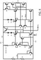
- FIG. 4 shows a circuit diagram for the floating ground voltage generator circuit 150 powered from the supply voltage Vdd at node 200 and the reference voltage Gnd at node 202.
- a resistive voltage divider formed by series connected resistors R1 and R2 generates an intermediate voltage Vth.
- a diode-connected n-channel MOSFET device M1 is coupled between the tap node of the resistive voltage divider and the node 202, with the source of device M1 connected to node 202 and the gate and drain of device M1 connected to the tap node of the resistive voltage divider.
- An n-channel MOSFET device M2 has a gate coupled to the gate of device M1 and a source connected to node 202.
- a resistor R4 has a first terminal connected to the drain of device M2 and a second terminal connected to the drain of a p-channel MOSFET device M14.
- the gate of device M14 is connected to the first terminal of the resistor R4.
- the source of device M14 is connected to the source (and body) of a diode connected n-channel MOSFET device M6.
- a second terminal of resistor Rth is connected to the node 200.
- An n-channel MOSFET device M3 has a gate coupled to the gate of device M1 and a source connected to node 202.
- An n-channel MOSFET device M7 has a source and body connected to the drain of device M3 at floating ground output node 204 and a gate coupled to the gate of diode-connected device M6.
- a plurality of diodes D1, D2, ..., Dx are connected in series (head to tail) between node 200 and the drain of device M7.
- the cathode of diode D1 is connected to the drain of device M7 and the anode of diode Dx is connected to node 200.
- a p-channel MOSFET Mt1 has a source connected to the floating ground output node 204, a drain connected to node 202 and a gate connected to the drain of device M14 and the second terminal of resistor R4.
- a MOSFET device Md configured as a capacitor, is coupled between the floating ground output node 204 and the node 200, with the gate of device Md connected to node 204 and the source and drain of device Md connected to node 200.
- the floating ground voltage Vfg is generated at the output node 204.
- a p-channel MOSFET device Mt2 has a drain connected to node 202, a source connected to floating ground output node 204 and a gate connected to replica output node 206 (where a replica floating ground output voltage Vfgrep that is substantially equal to voltage Vfg is generated).
- An n-channel MOSFET device Mt3 has a drain connected to node 200, a source connected to replica output node 204 and a gate.
- An n-channel MOSFET device M4 has a gate coupled to the gate of device M1, a source connected to node 202 and a drain connected to replica output node 206.
- An n-channel MOSFET device M8 has a source and body connected to the drain of device M4 at replica output node 206 and a gate coupled to the gate of diode-connected device M6.
- a plurality of replica diodes D1r, D2r, ..., Dxr are connected in series (head to tail) between node 200 and the drain of device M8. Specifically, the cathode of diode D1r is connected to the drain of device M8 and the anode of diode Dxr is connected to node 200.
- An n-channel MOSFET device M5 has a gate coupled to the gate of device M1 and a source connected to node 202.
- An n-channel MOSFET device M9 has a source and body connected to the drain of device M5 and a gate coupled to the gate of diode-connected device M6.
- a diode connected p-channel MOSFET device M10 has a drain and gate connected to the drain of device M9, and a source connected to node 200.
- a p-channel MOSFET device M11 has a gate coupled to the gate of device M10 and a source connected to node 200.
- a p-channel MOSFET device M12 has a source connected to the drain of device M11 and a gate connected to the replica output node 206.
- a resistor R3 has a first terminal connected to the drain of device M12 and a second terminal connected to the drain of an n-channel MOSFET device M13 and the gate of device Mt3.
- the gate of device M13 is connected to the first terminal of the resistor R3 at the drain of device M12.
- the non-linear behavior of the variable voltage generation by the floating ground voltage generator circuit 150 in generating the floating ground voltage Vfg is controlled in the following manner.
- the plurality of diodes D1, D2, ..., Dx function to ensure that the floating ground voltage Vfg tracks the reference voltage Gnd over the first range 170 of supply voltage Vdd levels.
- the voltage level of the floating ground voltage Vfg at the output node 204 is blocked by the diodes D1, D2, ..., Dx from rising above the reference voltage Gnd until the level of the supply voltage Vdd exceeds the sum of the threshold voltages of the diodes D1, D2, ..., Dx. This ensures that the maximum drive is available to the high side gate driver circuit 132 in the first range 170 of voltages.
- a current mirror formed by n-channel MOSFET devices M1, M2, M3, M4 and M5 mirrors the current Ith.
- the gate-to-source voltage of device M6 is then also equal to the gate-to-source voltage of devices M1 and M2 (if the body and source of device M6 are tied together). This ensures that the voltage drop from supply voltage Vdd to the floating ground voltage Vfg over the second range 172 of supply voltage Vdd levels is equal to Vth (in other words, the voltage tracks the ratio metric relationship set by the resistive voltage divider).
- the circuit formed by resistor R4 and device M14 provides a DC bias to the gate of device M14 so that this transistor is biased on the edge of conduction.
- the replica floating ground voltage Vfgrep is generated and bias voltages are provided at the gates of devices Mt2 and Mt3 so that these transistors are biased on the edge of conduction.
- the gate-to-source voltage of device Mt1 will increase and start conducting the current from voltage node 200 to be dumped at the output node 204 to raise the floating ground voltage Vfg back towards the desired target voltage level.
- the capacitor configured device Md decouples the output node 204 from any instantaneous switching currents.
- FIG. 5 shows a circuit diagram for the floating supply voltage generator circuit 152 powered from the supply voltage Vdd at node 200 and the reference voltage Gnd at node 202.
- a resistive voltage divider formed by series connected resistors R1' and R2' generates an intermediate voltage Vth'.
- a diode-connected p-channel MOSFET device M1' is coupled between the tap node of the resistive voltage divider and the node 200, with the source of device M1' connected to node 200 and the gate and drain of device M1' connected to the tap node of the resistive voltage divider.
- a p-channel MOSFET device M2' has a gate coupled to the gate of device M1' and a source connected to node 200.
- a resistor R4' has a first terminal connected to the drain of device M2' and a second terminal connected to the drain of an n-channel MOSFET device M14'.
- the gate of device M14' is connected to the first terminal of the resistor R4'.
- the source of device M14' is connected to the source (and body) of a diode connected p-channel MOSFET device M6'.
- a second terminal of resistor Rth' is connected to the node 202.
- a p-channel MOSFET device M3' has a gate coupled to the gate of device M1' and a source connected to node 200.
- a p-channel MOSFET device M7' has a source and body connected to the drain of device M3 at floating ground output node 204 and a gate coupled to the gate of diode-connected device M6'.
- a plurality of diodes D1', D2', ..., Dx' are connected in series (head to tail) between node 202 and the drain of device M7'. Specifically, the cathode of diode D1' is connected to node 202 and the anode of diode Dx' is connected to the drain of device M7'.
- An n-channel MOSFET Mt1' has a source connected to the floating supply output node 204', a drain connected to node 200 and a gate connected to the drain of device M14' and the second terminal of resistor R4'.
- a MOSFET device Md' configured as a capacitor, is coupled between the floating supply output node 204' and the node 202, with the gate of device Md' connected to node 204' and the source and drain of device Md' connected to node 200.
- the floating supply voltage Vfs is generated at the output node 204'.
- An n-channel MOSFET device Mt2' has a drain connected to node 200, a source connected to floating supply output node 204' and a gate connected to replica output node 206' (where a replica floating supply output voltage Vfsrep that is substantially equal to voltage Vfs is generated).
- a p-channel MOSFET device Mt3 has a drain connected to node 202, a source connected to replica output node 204' and a gate.
- a p-channel MOSFET device M4' has a gate coupled to the gate of device M1', a source connected to node 200 and a drain connected to replica output node 206'.
- a p-channel MOSFET device M8' has a source and body connected to the drain of device M4' at replica output node 206' and a gate coupled to the gate of diode-connected device M6'.
- a plurality of replica diodes D1r', D2r', ..., Dxr' are connected in series (head to tail) between node 202 and the drain of device M8'. Specifically, the cathode of diode D1r' is connected to node 202 and the anode of diode Dxr' is connected to the drain of device M8'.
- a p-channel MOSFET device M5' has a gate coupled to the gate of device M1' and a source connected to node 200.
- a p-channel MOSFET device M9' has a source and body connected to the drain of device M5' and a gate coupled to the gate of diode-connected device M6'.
- a diode connected n-channel MOSFET device M10' has a drain and gate connected to the drain of device M9', and a source connected to node 202.
- An n-channel MOSFET device M11' has a gate coupled to the gate of device M10' and a source connected to node 202.
- An n-channel MOSFET device M12' has a source connected to the drain of device M11' and a gate connected to the replica output node 206'.
- a resistor R3' has a first terminal connected to the drain of device M12' and a second terminal connected to the drain of a p-channel MOSFET device M13' and the gate of device Mt3'.
- the gate of device M13' is connected to the first terminal of the resistor R3' at the drain of device M12'.
- the non-linear behavior of the variable voltage generation by the floating supply voltage generator circuit 152 in generating the floating supply voltage Vfs is controlled in the following manner.
- the plurality of diodes D1', D2', ..., Dx' function to ensure that the floating supply voltage Vfs tracks the supply voltage Vdd over the first range 170 of supply voltage Vdd levels.
- the voltage level of the floating supply voltage Vfs at the output node 204' is blocked by the diodes D1', D2,' ..., Dx' from falling below the supply voltage Vdd until the level of the supply voltage Vdd exceeds the sum of the threshold voltages of the diodes D1', D2', ...Dx'. This ensures that the maximum drive is available to the low side gate driver circuit 134 over the first 170 of voltages.
- the values of the resistances for the resistors R1' and R2' are chosen so that the intermediate voltage Vth' at the tap node of the resistive voltage divider is equal to the supply voltage Vdd minus the targeted DC voltage level of the floating supply voltage Vfs.
- Vth (Vdd*R1)/(R1+R2). So, for the floating supply voltage Vfs equal to (2*(Vdd-Gnd))/3), the intermediate voltage Vth' will equal (Vdd-Gnd)/3).
- a current mirror formed by n-channel MOSFET devices M1', M2', M3', M4' and M5' mirrors the current Ith.
- the gate-to-source voltage of device M6' is then also equal to the gate-to-source voltage of devices M1' and M2' (if the body and source of device M6' are tied together). This ensures that the voltage drop from supply voltage Vdd to the floating supply voltage Vfs over the second range 172 of supply voltage Vdd levels is equal to Vth' (in other words, the voltage tracks the ratio metric relationship set by the resistive voltage divider).
- the MOSFET devices Mtl', Mt2' and Mt3' which are biased to operate in near conduction (or almost off), are selectively turned on to dissipate the transient.
- the circuit formed by resistor R4' and device M14' provides a DC bias to the gate of device M14' so that this transistor is biased on the edge of conduction.
- the replica floating supply voltage Vfsrep is generated and bias voltages are provided at the gates of devices Mt2' and Mt3' so that these transistors are biased on the edge of conduction.
- the gate-to-source voltage of device Mt1' will increase and start conducting the current from voltage node 200 to be dumped at the output node 204' to lower the floating supply voltage Vfs back towards the desired target voltage level.
- the capacitor configured device Md' decouples the output node 204' from any instantaneous switching currents.
Landscapes
- Engineering & Computer Science (AREA)
- Power Engineering (AREA)
- Dc-Dc Converters (AREA)
Abstract

Description
- This disclosure is related to the field of DC-DC voltage converters and, in particular, to the biasing of cascode transistors within an output bridge circuit.
-
Figure 1 shows a circuit diagram of a conventional DC-DCvoltage converter circuit 10. Thevoltage converter circuit 10 includes a transistor bridge circuit including a high sidetransistor drive circuit 12 and a low sidetransistor drive circuit 14 coupled in series with each other between asupply voltage node 16 providing a supply voltage Vdd and areference voltage node 18 providing a reference voltage Gnd. The current conduction paths through the high sidetransistor drive circuit 12 and the low sidetransistor drive circuit 14 are connected at a switchedoutput node 20. The high sidetransistor drive circuit 12 may, for example, comprise a p-channel power metal oxide semiconductor field effect transistor (MOSFET) device MP1 having a source terminal connected tosupply voltage node 16 and a drain terminal connected to the switchedoutput node 20. The low sidetransistor drive circuit 14 may, for example, comprise an n-channel power MOSFET device MN1 having a source terminal connected toreference voltage node 18 and a drain terminal connected to the switchedoutput node 20. The high sidetransistor drive circuit 12 is driven by a high side drive signal pgate that is output by a high sidegate driver circuit 32. The low sidetransistor drive circuit 14 is driven by a low side drive signal ngate that is output by a low sidegate driver circuit 34. A pulse width modulation (PWM)control circuit 38 generates non-overlapping PWM control signals p-PWM and n-PWM that are applied, respectively, to the inputs of the high sidegate driver circuit 32 and the low sidegate driver circuit 34 which then output the high side drive signal pgate and the low side drive signal ngate. - In an implementation where the DC-DC
voltage converter circuit 10 is a buck converter, an inductor L has a first terminal connected to the switchedoutput node 20 and a second terminal connected to aDC output node 40 where an output voltage Vout is generated and applied to a load (represented by capacitor C). The output voltage Vout is sensed by avoltage sensing circuit 44 to generate a feedback voltage Vfb. Thevoltage sensing circuit 44 may, for example, comprise a resistive divider circuit. ThePWM control circuit 38 uses the feedback voltage Vfb to control the pulse widths of the non-overlapping PWM control signals p-PWM and n-PWM and thus regulate a voltage level of the output voltage Vout. - This summary is provided to introduce a selection of concepts that are further described below in the detailed description. This summary is not intended to identify key or essential features of the claimed subject matter, nor is it intended to be used as an aid in limiting the scope of the claimed subject matter.
- In an embodiment, a circuit is powered by a power supply voltage and a reference voltage and comprises: a power transistor; a cascode transistor; wherein the power transistor and cascode transistor are connected in series; a driver circuit having an output driving a control terminal of the power transistor, wherein the driver circuit has a first power supply node coupled to receive a floating voltage that is also applied to a control terminal of the cascode transistor; and a variable voltage generator configured to generate the floating voltage, said variable voltage generator generating the floating voltage to track either the power supply voltage or the reference voltage over a first range of voltage levels for said power supply voltage and further generating the floating voltage to satisfy a ratio metric relationship dependent on the power supply voltage and reference voltage over a second range of voltage levels for said power supply voltage.
- In an embodiment, a circuit comprises: a high side power transistor; a high side cascode transistor; wherein the high side power transistor and high side cascode transistor are connected in series between a power supply voltage and a switching node; a low side power transistor; a low side cascode transistor; wherein the low side power transistor and low side cascode transistor are connected in series between the switching node and a reference voltage; a high side driver circuit having an output driving a control terminal of the high side power transistor, wherein the high side driver circuit has a first power supply node coupled to receive the power supply voltage and a second power supply node coupled to receive a floating ground voltage that is also applied to a control terminal of the high side cascode transistor; a low side driver circuit having an output driving a control terminal of the low side power transistor, wherein the low side driver circuit has a first power supply node coupled to receive a floating supply voltage that is also applied to a control terminal of the low side cascode transistor and a second power supply node coupled to receive the reference voltage. A first variable voltage generator is configured to generate the floating ground voltage, wherein the floating ground voltage tracks the reference voltage over a first range of voltage levels for said power supply voltage and further satisfies a first ratio metric relationship dependent on the power supply voltage and reference voltage over a second range of voltage levels for said power supply voltage. A second variable voltage generator is configured to generate the floating supply voltage, wherein the floating supply voltage tracks the power supply voltage over the first range of voltage levels for said power supply voltage and further satisfies a second ratio metric relationship dependent on the power supply voltage and reference voltage over the second range of voltage levels for said power supply voltage. The first and second ratio metric relationships are different.
-
-
Figure 1 is a circuit diagram of a conventional DC-DC voltage converter circuit. -
Figure 2 is a circuit diagram of a DC-DC voltage converter circuit. -
Figure 3 is a graph illustrating a relationship between supply voltage level and floating ground level and between supply voltage level and floating supply level. -
Figure 4 is a circuit diagram for a floating ground voltage generator for cascode biasing. -
Figure 5 is a circuit diagram for a floating supply voltage generator for cascode biasing. - In the following detailed description and the attached drawings, specific details are set forth to provide a thorough understanding of the present disclosure. However, those skilled in the art will appreciate that the present disclosure may be practiced, in some instances, without such specific details. In other instances, well-known elements have been illustrated in schematic or block diagram form in order not to obscure the present disclosure in unnecessary detail. Additionally, for the most part, specific details, and the like, have been omitted inasmuch as such details are not considered necessary to obtain a complete understanding of the present disclosure, and are considered to be within the understanding of persons of ordinary skill in the relevant art.
- Reference is now made to
Figure 2 which shows a circuit diagram of a DC-DCvoltage converter circuit 100. Thevoltage converter circuit 100 includes a transistor bridge circuit including a high sidetransistor drive circuit 112 and a low sidetransistor drive circuit 114 coupled in series with each other between asupply voltage node 116 providing a supply voltage Vdd and areference voltage node 118 providing a reference voltage Gnd. The current conduction paths through the high sidetransistor drive circuit 112 and the low sidetransistor drive circuit 114 are connected at a switchedoutput node 120. The high sidetransistor drive circuit 112 comprises a p-channel power metal oxide semiconductor field effect transistor (MOSFET) device MP1 having a source terminal connected tosupply voltage node 116 and a drain terminal and a p-channel cascode MOSFET device MP2 having a drain terminal connected to the switchedoutput node 120 and a source terminal connected to the drain terminal of device MP1. The low sidetransistor drive circuit 114 comprises an n-channel power MOSFET device MN1 having a source terminal connected toreference voltage node 118 and a drain terminal and an n-channel cascode MOSFET device MN2 having a drain terminal connected to the switchedoutput node 120 and a source terminal connected to the drain terminal of device MN1. The use of cascode transistors MP2 and MN2 in the transistor bridge circuit supports operation of the DC-DCvoltage converter circuit 100 at higher voltage levels (for example, 8.0V) of the supply voltage Vdd. - The p-channel power MOSFET device MP1 is driven by a high side drive signal pgate that is output by a high side
gate driver circuit 132. The p-channel cascode MOSFET device MP2 is driven (i.e., biased) by a floating ground voltage Vfg that is generated by a floating groundvoltage generator circuit 150. The low sidetransistor drive circuit 114 is driven by a low side drive signal ngate that is output by a low sidegate driver circuit 134. The n-channel cascode MOSFET device MN2 is driven (i.e., biased) by a floating source voltage Vfs that is generated by a floating sourcevoltage generator circuit 152. A pulse width modulation (PWM)control circuit 138 generates non-overlapping PWM control signals p-PWM and n-PWM that are applied, respectively, to the inputs of the high sidegate driver circuit 132 and the low sidegate driver circuit 134 which then output the high side drive signal pgate and the low side drive signal ngate. - A diode Da has an anode coupled to the gate of p-channel cascode MOSFET device MP2 and a cathode connected to the series connection node between the drain of p-channel power MOSFET device MP1 and the source of p-channel cascode MOSFET device MP2. A diode Db has a cathode coupled to the gate of n-channel cascode MOSFET device MN2 and an anode connected to the series connection node between the drain of n-channel power MOSFET device MN1 and the source of n-channel cascode MOSFET device MN2. The diodes Da and Db address a reliability concern which arises due to leakage of the MOSFETs. In this regard, when the leakage of transistor MP2 exceeds the leakage of transistor MP1, the drain of transistor MP1 can discharge to an unacceptable voltage level (for example, 0V) leading to reliability concerns with transistor MP1. The diode D1 ensures that the source of transistor MP2 is kept at a voltage level where transistor MP1 is in a safe region of operation. The diode Db performs a similar function relative to transistor MN1.
- The power supply nodes of the high side
gate driver circuit 132 are connected to receive the supply voltage Vdd and the floating ground voltage Vfg. The high sidegate driver circuit 132 accordingly functions to level shift the PWM control signal p-PWM to generate the high side drive signal pgate having a voltage range between Vfg and Vdd. The power supply nodes of the low sidegate driver circuit 134 are connected to receive the floating source voltage Vfs and the reference voltage Gnd. The low sidegate driver circuit 134 accordingly functions to level shift the PWM control signal n-PWM to generate the low side drive signal ngate having a voltage range between Gnd and Vfs. - In an implementation where the DC-DC
voltage converter circuit 100 is a buck converter, an inductor L has a first terminal connected to the switchedoutput node 120 and a second terminal connected to aDC output node 140 where an output voltage Vout is generated and applied to a load (represented by capacitor C). The output voltage Vout is sensed by avoltage sensing circuit 44 to generate a feedback voltage Vfb. Thevoltage sensing circuit 144 may, for example, comprise a resistive divider circuit. ThePWM control circuit 138 uses the feedback voltage Vfb to control the pulse widths of the non-overlapping PWM control signals p-PWM and n-PWM and thus regulate a voltage level of the output voltage Vout. - The power supply nodes of the floating ground
voltage generator circuit 150 are connected to receive the supply voltage Vdd and the reference voltage Gnd. The floating groundvoltage generator circuit 150 is a variable voltage generator where the level of the floating ground voltage Vfg that is generated is dependent on the levels of the supply voltage Vdd and reference voltage Gnd. This is illustrated inFigure 3 . Over afirst range 170 of supply voltage Vdd levels (in the illustrated example, from 0V to about 2.5V), the level of the floating ground voltage Vfg tracks (i.e., follows, is substantially equal to) the reference voltage Gnd. Within the relatively lower supply voltage range shown byfirst range 170, the floating groundvoltage generator circuit 150 generates the bias voltage for the cascode transistor device MP2 so that a higher overdrive voltage is provided allowing the high sidegate driver circuit 132 to work reliably without exceeding the technology limits of the MOSFET safe operating area (SOA) voltages for the devices MP1 and MP2 of the high sidetransistor drive circuit 112. Over asecond range 172 of supply voltage Vdd levels (in the illustrated example, from about 2.5V to 8.0V), the level of the floating ground voltage Vfg is controlled to satisfy a first ratio metric relationship dependent on the levels of the supply voltage Vdd and the reference voltage Gnd (for example, the first ratio metric relationship may generally be a function of the ratio: (Vdd-Gnd)/3). Within the relatively higher supply voltage range shown byfirst range 172, the floating groundvoltage generator circuit 150 generates the bias voltage for the cascode transistor device MP2 so that the devices MP1 and MP2 of the high sidetransistor drive circuit 112 do not exceed the allowed MOSFET safe operating area (SOA) voltages. - The power supply nodes of the floating supply
voltage generator circuit 152 are connected to receive the supply voltage Vdd and the reference voltage Gnd. The floating supplyvoltage generator circuit 152 is a variable voltage generator where the level of the floating supply voltage Vfs that is generated is dependent on the levels of the supply voltage Vdd and reference voltage Gnd. This is illustrated inFigure 3 . Over thefirst range 170 of supply voltage Vdd levels (in the illustrated example, from 0V to about 2.5V), the level of the floating supply voltage Vfs tracks (i.e., follows, is substantially equal to) the reference voltage Gnd. Within the relatively lower supply voltage range shown byfirst range 170, the floating supplyvoltage generator circuit 152 generates the bias voltage for the cascode transistor device MN2 so that a higher overdrive voltage is provided allowing the low sidegate driver circuit 134 to work reliably without exceeding the technology limits of the MOSFET safe operating area (SOA) voltages for the devices MN1 and MN2 of the low sidetransistor drive circuit 114. Over thesecond range 172 of supply voltage Vdd levels (in the illustrated example, from about 2.5V to 8.0V), the level of the floating supply voltage Vfs is controlled to satisfy a second ratio metric relationship dependent on the levels of the supply voltage Vdd and the reference voltage Gnd (for example, the second ratio metric relationship may generally be a function of the ratio: (2*(Vdd-Gnd))/3). Within the relatively higher supply voltage range shown byfirst range 172, the floating supplyvoltage generator circuit 152 generates the bias voltage for the cascode transistor device MN2 so that the devices MN1 and MN2 of the low sidetransistor drive circuit 114 do not exceed the allowed MOSFET safe operating area (SOA) voltages. - Reference is now made to
Figure 4 which shows a circuit diagram for the floating groundvoltage generator circuit 150 powered from the supply voltage Vdd atnode 200 and the reference voltage Gnd atnode 202. A resistive voltage divider formed by series connected resistors R1 and R2 generates an intermediate voltage Vth. A diode-connected n-channel MOSFET device M1 is coupled between the tap node of the resistive voltage divider and thenode 202, with the source of device M1 connected tonode 202 and the gate and drain of device M1 connected to the tap node of the resistive voltage divider. An n-channel MOSFET device M2 has a gate coupled to the gate of device M1 and a source connected tonode 202. A resistor R4 has a first terminal connected to the drain of device M2 and a second terminal connected to the drain of a p-channel MOSFET device M14. The gate of device M14 is connected to the first terminal of the resistor R4. The source of device M14 is connected to the source (and body) of a diode connected n-channel MOSFET device M6. The gate and drain of device M6 are connected to the first terminal of a resistor Rth, where Rth=R1∥R2. A second terminal of resistor Rth is connected to thenode 200. An n-channel MOSFET device M3 has a gate coupled to the gate of device M1 and a source connected tonode 202. An n-channel MOSFET device M7 has a source and body connected to the drain of device M3 at floatingground output node 204 and a gate coupled to the gate of diode-connected device M6. A plurality of diodes D1, D2, ..., Dx are connected in series (head to tail) betweennode 200 and the drain of device M7. Specifically, the cathode of diode D1 is connected to the drain of device M7 and the anode of diode Dx is connected tonode 200. A p-channel MOSFET Mt1 has a source connected to the floatingground output node 204, a drain connected tonode 202 and a gate connected to the drain of device M14 and the second terminal of resistor R4. A MOSFET device Md, configured as a capacitor, is coupled between the floatingground output node 204 and thenode 200, with the gate of device Md connected tonode 204 and the source and drain of device Md connected tonode 200. The floating ground voltage Vfg is generated at theoutput node 204. A p-channel MOSFET device Mt2 has a drain connected tonode 202, a source connected to floatingground output node 204 and a gate connected to replica output node 206 (where a replica floating ground output voltage Vfgrep that is substantially equal to voltage Vfg is generated). An n-channel MOSFET device Mt3 has a drain connected tonode 200, a source connected toreplica output node 204 and a gate. An n-channel MOSFET device M4 has a gate coupled to the gate of device M1, a source connected tonode 202 and a drain connected toreplica output node 206. An n-channel MOSFET device M8 has a source and body connected to the drain of device M4 atreplica output node 206 and a gate coupled to the gate of diode-connected device M6. A plurality of replica diodes D1r, D2r, ..., Dxr are connected in series (head to tail) betweennode 200 and the drain of device M8. Specifically, the cathode of diode D1r is connected to the drain of device M8 and the anode of diode Dxr is connected tonode 200. An n-channel MOSFET device M5 has a gate coupled to the gate of device M1 and a source connected tonode 202. An n-channel MOSFET device M9 has a source and body connected to the drain of device M5 and a gate coupled to the gate of diode-connected device M6. A diode connected p-channel MOSFET device M10 has a drain and gate connected to the drain of device M9, and a source connected tonode 200. A p-channel MOSFET device M11 has a gate coupled to the gate of device M10 and a source connected tonode 200. A p-channel MOSFET device M12 has a source connected to the drain of device M11 and a gate connected to thereplica output node 206. A resistor R3 has a first terminal connected to the drain of device M12 and a second terminal connected to the drain of an n-channel MOSFET device M13 and the gate of device Mt3. The gate of device M13 is connected to the first terminal of the resistor R3 at the drain of device M12. - The non-linear behavior of the variable voltage generation by the floating ground
voltage generator circuit 150 in generating the floating ground voltage Vfg (see,Figure 3 ) is controlled in the following manner. The plurality of diodes D1, D2, ..., Dx function to ensure that the floating ground voltage Vfg tracks the reference voltage Gnd over thefirst range 170 of supply voltage Vdd levels. The voltage level of the floating ground voltage Vfg at theoutput node 204 is blocked by the diodes D1, D2, ..., Dx from rising above the reference voltage Gnd until the level of the supply voltage Vdd exceeds the sum of the threshold voltages of the diodes D1, D2, ..., Dx. This ensures that the maximum drive is available to the high sidegate driver circuit 132 in thefirst range 170 of voltages. - The values of the resistances for the resistors R1 and R2 are chosen so that the intermediate voltage Vth at the tap node of the resistive voltage divider is equal to the supply voltage Vdd minus the targeted DC voltage level of the floating ground voltage Vfg. In other words, Vth=(Vdd*R1)/(R1+R2). So, for the floating ground voltage Vfg equal to (Vdd-Gnd)/3), the intermediate voltage Vth will equal (2*(Vdd-Gnd))/3). The current flowing through device M1 is equal to Ith=(Vth-Vgs)Rth (where Rth=R1∥R2 and Vgs is the gate-to-source voltage of device M1). A current mirror formed by n-channel MOSFET devices M1, M2, M3, M4 and M5 mirrors the current Ith. For the same current in devices M1 and M2, the gate-to-source voltage of device M6 is then also equal to the gate-to-source voltage of devices M1 and M2 (if the body and source of device M6 are tied together). This ensures that the voltage drop from supply voltage Vdd to the floating ground voltage Vfg over the
second range 172 of supply voltage Vdd levels is equal to Vth (in other words, the voltage tracks the ratio metric relationship set by the resistive voltage divider). - To address concerns with large transient currents, the MOSFET devices Mt1, Mt2 and Mt3, which are biased to operate in near conduction (or almost off), are selectively turned on to dissipate the transient. The circuit formed by resistor R4 and device M14 provides a DC bias to the gate of device M14 so that this transistor is biased on the edge of conduction. Similarly, the replica floating ground voltage Vfgrep is generated and bias voltages are provided at the gates of devices Mt2 and Mt3 so that these transistors are biased on the edge of conduction. As an example of the transient current response operation, when transient current is drawn from the floating
ground output node 204, the gate-to-source voltage of device Mt1 will increase and start conducting the current fromvoltage node 200 to be dumped at theoutput node 204 to raise the floating ground voltage Vfg back towards the desired target voltage level. The capacitor configured device Md decouples theoutput node 204 from any instantaneous switching currents. - Reference is now made to
Figure 5 which shows a circuit diagram for the floating supplyvoltage generator circuit 152 powered from the supply voltage Vdd atnode 200 and the reference voltage Gnd atnode 202. A resistive voltage divider formed by series connected resistors R1' and R2' generates an intermediate voltage Vth'. A diode-connected p-channel MOSFET device M1' is coupled between the tap node of the resistive voltage divider and thenode 200, with the source of device M1' connected tonode 200 and the gate and drain of device M1' connected to the tap node of the resistive voltage divider. A p-channel MOSFET device M2' has a gate coupled to the gate of device M1' and a source connected tonode 200. A resistor R4' has a first terminal connected to the drain of device M2' and a second terminal connected to the drain of an n-channel MOSFET device M14'. The gate of device M14' is connected to the first terminal of the resistor R4'. The source of device M14' is connected to the source (and body) of a diode connected p-channel MOSFET device M6'. The gate and drain of device M6' are connected to the first terminal of a resistor Rth', where Rth'=R1'∥R2'. A second terminal of resistor Rth' is connected to thenode 202. A p-channel MOSFET device M3' has a gate coupled to the gate of device M1' and a source connected tonode 200. A p-channel MOSFET device M7' has a source and body connected to the drain of device M3 at floatingground output node 204 and a gate coupled to the gate of diode-connected device M6'. A plurality of diodes D1', D2', ..., Dx' are connected in series (head to tail) betweennode 202 and the drain of device M7'. Specifically, the cathode of diode D1' is connected tonode 202 and the anode of diode Dx' is connected to the drain of device M7'. An n-channel MOSFET Mt1' has a source connected to the floating supply output node 204', a drain connected tonode 200 and a gate connected to the drain of device M14' and the second terminal of resistor R4'. A MOSFET device Md', configured as a capacitor, is coupled between the floating supply output node 204' and thenode 202, with the gate of device Md' connected to node 204' and the source and drain of device Md' connected tonode 200. The floating supply voltage Vfs is generated at the output node 204'. An n-channel MOSFET device Mt2' has a drain connected tonode 200, a source connected to floating supply output node 204' and a gate connected to replica output node 206' (where a replica floating supply output voltage Vfsrep that is substantially equal to voltage Vfs is generated). A p-channel MOSFET device Mt3 has a drain connected tonode 202, a source connected to replica output node 204' and a gate. A p-channel MOSFET device M4' has a gate coupled to the gate of device M1', a source connected tonode 200 and a drain connected to replica output node 206'. A p-channel MOSFET device M8' has a source and body connected to the drain of device M4' at replica output node 206' and a gate coupled to the gate of diode-connected device M6'. A plurality of replica diodes D1r', D2r', ..., Dxr' are connected in series (head to tail) betweennode 202 and the drain of device M8'. Specifically, the cathode of diode D1r' is connected tonode 202 and the anode of diode Dxr' is connected to the drain of device M8'. A p-channel MOSFET device M5' has a gate coupled to the gate of device M1' and a source connected tonode 200. A p-channel MOSFET device M9' has a source and body connected to the drain of device M5' and a gate coupled to the gate of diode-connected device M6'. A diode connected n-channel MOSFET device M10' has a drain and gate connected to the drain of device M9', and a source connected tonode 202. An n-channel MOSFET device M11' has a gate coupled to the gate of device M10' and a source connected tonode 202. An n-channel MOSFET device M12' has a source connected to the drain of device M11' and a gate connected to the replica output node 206'. A resistor R3' has a first terminal connected to the drain of device M12' and a second terminal connected to the drain of a p-channel MOSFET device M13' and the gate of device Mt3'. The gate of device M13' is connected to the first terminal of the resistor R3' at the drain of device M12'. - The non-linear behavior of the variable voltage generation by the floating supply
voltage generator circuit 152 in generating the floating supply voltage Vfs (see,Figure 3 ) is controlled in the following manner. The plurality of diodes D1', D2', ..., Dx' function to ensure that the floating supply voltage Vfs tracks the supply voltage Vdd over thefirst range 170 of supply voltage Vdd levels. The voltage level of the floating supply voltage Vfs at the output node 204' is blocked by the diodes D1', D2,' ..., Dx' from falling below the supply voltage Vdd until the level of the supply voltage Vdd exceeds the sum of the threshold voltages of the diodes D1', D2', ...Dx'. This ensures that the maximum drive is available to the low sidegate driver circuit 134 over the first 170 of voltages. - The values of the resistances for the resistors R1' and R2' are chosen so that the intermediate voltage Vth' at the tap node of the resistive voltage divider is equal to the supply voltage Vdd minus the targeted DC voltage level of the floating supply voltage Vfs. In other words, Vth=(Vdd*R1)/(R1+R2). So, for the floating supply voltage Vfs equal to (2*(Vdd-Gnd))/3), the intermediate voltage Vth' will equal (Vdd-Gnd)/3). The current flowing through device M1' is equal to Ith=(Vth'-Vgs)Rth' (where Rth'=R1∥R2 and Vgs is the gate-to-source voltage of device M1'). A current mirror formed by n-channel MOSFET devices M1', M2', M3', M4' and M5' mirrors the current Ith. For the same current in devices M1' and M2', the gate-to-source voltage of device M6' is then also equal to the gate-to-source voltage of devices M1' and M2' (if the body and source of device M6' are tied together). This ensures that the voltage drop from supply voltage Vdd to the floating supply voltage Vfs over the
second range 172 of supply voltage Vdd levels is equal to Vth' (in other words, the voltage tracks the ratio metric relationship set by the resistive voltage divider). - To address concerns with large transient currents, the MOSFET devices Mtl', Mt2' and Mt3', which are biased to operate in near conduction (or almost off), are selectively turned on to dissipate the transient. The circuit formed by resistor R4' and device M14' provides a DC bias to the gate of device M14' so that this transistor is biased on the edge of conduction. Similarly, the replica floating supply voltage Vfsrep is generated and bias voltages are provided at the gates of devices Mt2' and Mt3' so that these transistors are biased on the edge of conduction. As an example of the transient current response operation, when transient current is sourced to from the floating supply output node 204', the gate-to-source voltage of device Mt1' will increase and start conducting the current from
voltage node 200 to be dumped at the output node 204' to lower the floating supply voltage Vfs back towards the desired target voltage level. The capacitor configured device Md' decouples the output node 204' from any instantaneous switching currents. - Although the preceding description has been described herein with reference to particular circuits and embodiments, it is not intended to be limited to the particulars disclosed herein; rather, it extends to all functionally equivalent structures, methods, and uses, such as are within the scope of the appended claims.
Claims (19)
- A circuit powered by a power supply voltage (Vdd) and a reference voltage (Gnd), comprising:a power transistor (MP1, MN1);a cascode transistor (MP2, MN2);wherein the power transistor (MP1, MN1) and cascode transistor (MP2, MN2) are connected in series;a driver circuit (132, 134) having an output driving a control terminal of the power transistor, wherein the driver circuit has a first power supply node coupled to receive a floating voltage (Vfg, Vfs) that is also applied to a control terminal of the cascode transistor; anda variable voltage generator (150, 152) configured to generate the floating voltage, said variable voltage generator generating the floating voltage to track either the power supply voltage (Vdd) or the reference voltage (Gnd) over a first range (170) of voltage levels for said power supply voltage and further generating the floating voltage to satisfy a ratio metric relationship dependent on the power supply voltage (Vdd) and reference voltage (Gnd) over a second range (172) of voltage levels for said power supply voltage.
- The circuit of claim 1, wherein the power transistor (MP1) and cascode transistor (MP2) are part of a high side driver circuit (112) coupled to a switching node (120), and wherein the driver circuit has a second power supply node coupled to receive the power supply voltage (Vdd).
- The circuit of claim 2, wherein the variable voltage generator includes a resistive voltage divider (R1, R2) coupled between the power supply voltage (Vdd) and the reference voltage (Gnd), said resistive voltage divider (R1, R2) generating an intermediate voltage (Vth) that controls setting of the ratio metric relationship.
- The circuit of claim 3, wherein the variable voltage generator further includes a plurality of diodes (D1, D2) connected in series, and wherein the plurality of diodes set a voltage level that delimits an upper end of the first range of voltage levels (170) where the floating voltage tracks the reference voltage (Gnd).
- The circuit of claim 3, wherein the ratio metric relationship sets the floating voltage as a function of a difference between the power supply voltage (Vdd) and the intermediate voltage (Vth).
- The circuit of claim 2, further comprising an inductor (L) having a first terminal coupled to the switching node and a second terminal coupled to an output node (140) where a DC-DC converted output voltage (Vout) is generated.
- The circuit of claim 1, wherein the power transistor (MN1) and cascode transistor (MN2) are part of a low side driver circuit (114) coupled to a switching node (120), and wherein the driver circuit has a second power supply node coupled to receive the reference voltage (Gnd).
- The circuit of claim 7, wherein the variable voltage generator includes a resistive voltage divider (R1', R2') coupled between the power supply voltage (Vdd) and the reference voltage (Gnd), said resistive voltage generating an intermediate voltage (Vth') that controls setting of the ratio metric relationship.
- The circuit of claim 8, wherein the variable voltage generator further includes a plurality of diodes (D1', D2') connected in series, and wherein the plurality of diodes set a voltage level that delimits an upper end of the first range of voltage levels (170) where the floating voltage tracks the power supply voltage (Vdd).
- The circuit of claim 8, wherein the ratio metric relationship sets the floating voltage as a function of a difference between the power supply voltage (Vdd) and the intermediate voltage (Vth').
- The circuit of claim 7, further comprising an inductor (L) having a first terminal coupled to the switching node and a second terminal coupled to an output node (140) where a DC-DC converted output voltage (Vout) is generated.
- A circuit, comprising:a high side power transistor (MP1);a high side cascode transistor (MP2);wherein the high side power transistor (MP1) and high side cascode transistor (MP2) are connected in series between a power supply voltage (Vdd) and a switching node (120);a low side power transistor (MN1);a low side cascode transistor (MN2);wherein the low side power transistor (MN1) and low side cascode transistor (MN2) are connected in series between the switching node (120) and a reference voltage (Gnd);a high side driver circuit (132) having an output driving a control terminal of the high side power transistor (MP1), wherein the high side driver circuit (132) has a first power supply node coupled to receive the power supply voltage (Vdd) and a second power supply node coupled to receive a floating ground voltage (Vfg) that is also applied to a control terminal of the high side cascode transistor (MP2);a low side driver circuit (134) having an output driving a control terminal of the low side power transistor (MN1), wherein the low side driver circuit (134) has a first power supply node coupled to receive a floating supply voltage (Vfs) that is also applied to a control terminal of the low side cascode transistor (MN2) and a second power supply node coupled to receive the reference voltage (Gnd);a first variable voltage generator (15) configured to generate the floating ground voltage (Vfg), wherein the floating ground voltage tracks the reference voltage (Gnd) over a first range of voltage levels (170) for said power supply voltage (Vdd) and further satisfies a first ratio metric relationship dependent on the power supply voltage (Vdd) and reference voltage (Gnd) over a second range of voltage levels (172) for said power supply voltage (VdD); anda second variable voltage generator (152) configured to generate the floating supply voltage (Vfs), wherein the floating supply voltage (Vfs) tracks the power supply voltage (Vdd) over the first range of voltage levels (170) for said power supply voltage (Vdd) and further satisfies a second ratio metric relationship dependent on the power supply voltage (Vdd) and reference voltage (Gnd) over the second range of voltage levels (172) for said power supply voltage (Vdd);wherein the first and second ratio metric relationships are different.
- The circuit of claim 12, wherein the first variable voltage generator (15) includes a resistive voltage divider (R1, R2) coupled between the power supply voltage (Vdd) and the reference voltage (Gnd), said resistive voltage divider (R1, R2) generating an intermediate voltage (Vth) that controls setting of the first ratio metric relationship.
- The circuit of claim 13, wherein the first variable voltage generator further includes a plurality of diodes (D1, D2) connected in series, and wherein the plurality of diodes set a voltage level that delimits an upper end of the first range of voltage levels where the floating ground voltage (Vfg) tracks the reference voltage (Gnd).
- The circuit of claim 13, wherein the first ratio metric relationship sets the floating ground voltage (Vfg) as a function of a difference between the power supply voltage (Vdd) and the intermediate voltage (Vth).
- The circuit of claim 12, wherein the second variable voltage generator includes a resistive voltage divider (R1', R2') coupled between the power supply voltage (Vdd) and the reference voltage (Gnd), said resistive voltage divider (R1', R2') generating an intermediate voltage (Vth') that controls setting of the second ratio metric relationship.
- The circuit of claim 16, wherein the second variable voltage generator further includes a plurality of diodes (D1', D2') connected in series, and wherein the plurality of diodes set a voltage level that delimits an upper end of the first range of voltage levels where the floating supply voltage (Vfs) tracks the power supply voltage (Vdd).
- The circuit of claim 17, wherein the second ratio metric relationship sets the floating voltage as a function of a difference between the power supply voltage (Vdd) and the intermediate voltage (Vth').
- The circuit of claim 12, further comprising an inductor (L) having a first terminal coupled to the switching node and a second terminal coupled to an output node (140) where a DC-DC converted output voltage (Vout) is generated.
Applications Claiming Priority (1)
| Application Number | Priority Date | Filing Date | Title |
|---|---|---|---|
| US17/016,588 US11606029B2 (en) | 2020-09-10 | 2020-09-10 | DC-DC voltage converter with floating rail generation for cascode transistor biasing |
Publications (2)
| Publication Number | Publication Date |
|---|---|
| EP3968518A1 true EP3968518A1 (en) | 2022-03-16 |
| EP3968518B1 EP3968518B1 (en) | 2024-04-10 |
Family
ID=77447816
Family Applications (1)
| Application Number | Title | Priority Date | Filing Date |
|---|---|---|---|
| EP21192626.6A Active EP3968518B1 (en) | 2020-09-10 | 2021-08-23 | Dc-dc voltage converter with floating rail generation for cascode transistor biasing |
Country Status (3)
| Country | Link |
|---|---|
| US (1) | US11606029B2 (en) |
| EP (1) | EP3968518B1 (en) |
| CN (1) | CN114257090A (en) |
Families Citing this family (7)
| Publication number | Priority date | Publication date | Assignee | Title |
|---|---|---|---|---|
| WO2020252561A1 (en) * | 2019-06-17 | 2020-12-24 | Smartd Technologies Inc. | Dynamic balancing of transistors |
| US11817771B2 (en) * | 2021-05-13 | 2023-11-14 | Qualcomm Incorporated | Gate driver having a floating supply node with selective power reception for use in switching converters |
| JP7830280B2 (en) * | 2022-09-26 | 2026-03-16 | 株式会社東芝 | Inrush current suppression circuit |
| EP4345571A1 (en) | 2022-09-30 | 2024-04-03 | Nxp B.V. | Bias circuit |
| GB2634791B (en) * | 2023-10-20 | 2026-03-25 | E Peas Sa | Power switching apparatus |
| US20260112955A1 (en) * | 2024-09-25 | 2026-04-23 | Stmicroelectronics International N.V. | Non-linear floating rail generation |
| US20260106618A1 (en) * | 2024-10-10 | 2026-04-16 | Stmicroelectronics International N.V. | High-voltage tolerant level shifter circuit |
Citations (2)
| Publication number | Priority date | Publication date | Assignee | Title |
|---|---|---|---|---|
| US5530394A (en) * | 1993-09-10 | 1996-06-25 | Deutsch Itt Industries Gmbh | CMOS circuit with increased breakdown strength |
| US20190334516A1 (en) * | 2016-09-23 | 2019-10-31 | Tohoku University | Switching circuit device, step-down dc-dc converter, and element unit |
Family Cites Families (14)
| Publication number | Priority date | Publication date | Assignee | Title |
|---|---|---|---|---|
| US5399960A (en) * | 1993-11-12 | 1995-03-21 | Cypress Semiconductor Corporation | Reference voltage generation method and apparatus |
| US5543740A (en) * | 1995-04-10 | 1996-08-06 | Philips Electronics North America Corporation | Integrated half-bridge driver circuit |
| US5973534A (en) * | 1998-01-29 | 1999-10-26 | Sun Microsystems, Inc. | Dynamic bias circuit for driving low voltage I/O transistors |
| KR100391991B1 (en) * | 2001-05-02 | 2003-07-22 | 삼성전자주식회사 | Semiconductor integrated circuit device with voltage interface circuit |
| US7960997B2 (en) * | 2007-08-08 | 2011-06-14 | Advanced Analogic Technologies, Inc. | Cascode current sensor for discrete power semiconductor devices |
| CN103187955B (en) * | 2011-12-31 | 2016-08-03 | 意法半导体研发(上海)有限公司 | Cascade drive circuit |
| CN106027014B (en) * | 2012-05-11 | 2019-10-01 | 意法半导体研发(深圳)有限公司 | Current slope control method and device for power driver circuit application |
| CN103036509B (en) * | 2012-12-17 | 2015-07-15 | 锐迪科创微电子(北京)有限公司 | Biasing circuit suitable for low noise amplifier |
| KR102492494B1 (en) * | 2014-12-09 | 2023-01-30 | 인피니언 테크놀로지스 오스트리아 아게 | A regulated high side gate driver circuit for power transistors |
| US10069439B2 (en) * | 2015-12-22 | 2018-09-04 | Renesas Electronics Corporation | Power conversion system, power module, and semiconductor device with diode coupling |
| US10164481B2 (en) * | 2016-11-21 | 2018-12-25 | Witricity Corporation | Current shunt monitor |
| US10291194B2 (en) * | 2017-10-09 | 2019-05-14 | Infineon Technologies Ag | System and method for biasing an RF circuit |
| US10168363B1 (en) * | 2018-03-14 | 2019-01-01 | STMicroelectronics Design & Application S.R.O. | Current sensor with extended voltage range |
| US10224922B1 (en) * | 2018-04-04 | 2019-03-05 | Stmicroelectronics International N.V. | Biasing cascode transistor of an output buffer circuit for operation over a wide range of supply voltages |
-
2020
- 2020-09-10 US US17/016,588 patent/US11606029B2/en active Active
-
2021
- 2021-08-23 EP EP21192626.6A patent/EP3968518B1/en active Active
- 2021-09-09 CN CN202111064684.8A patent/CN114257090A/en active Pending
Patent Citations (2)
| Publication number | Priority date | Publication date | Assignee | Title |
|---|---|---|---|---|
| US5530394A (en) * | 1993-09-10 | 1996-06-25 | Deutsch Itt Industries Gmbh | CMOS circuit with increased breakdown strength |
| US20190334516A1 (en) * | 2016-09-23 | 2019-10-31 | Tohoku University | Switching circuit device, step-down dc-dc converter, and element unit |
Also Published As
| Publication number | Publication date |
|---|---|
| EP3968518B1 (en) | 2024-04-10 |
| US11606029B2 (en) | 2023-03-14 |
| CN114257090A (en) | 2022-03-29 |
| US20220077776A1 (en) | 2022-03-10 |
Similar Documents
| Publication | Publication Date | Title |
|---|---|---|
| US11606029B2 (en) | DC-DC voltage converter with floating rail generation for cascode transistor biasing | |
| US6850044B2 (en) | Hybrid regulator with switching and linear sections | |
| US8604862B2 (en) | Four-quadrant bootstrapped switch circuit | |
| CN103152022B (en) | Reduce the MOSFET gate drivers of power consumption | |
| US8120338B2 (en) | Dropper-type regulator | |
| US7777472B2 (en) | Current detector circuit and current mode switching regulator | |
| JP7304729B2 (en) | Power supply circuit, power supply device and vehicle | |
| JP2000293248A (en) | Feedback controlled low voltage current sink / source | |
| CN210071919U (en) | Current sensing circuit and electronic circuit | |
| US20160268885A1 (en) | Using PMOS Power Switch In A Combination Switching And Linear Regulator | |
| US7576524B2 (en) | Constant voltage generating apparatus with simple overcurrent/short-circuit protection circuit | |
| US10498333B1 (en) | Adaptive gate buffer for a power stage | |
| JP2009060439A (en) | Error amplification circuit and switching power supply circuit | |
| JP2009075957A (en) | Power circuit and semiconductor device | |
| JP2009044304A (en) | Semiconductor element control device | |
| US9531259B2 (en) | Power supply circuit | |
| JP4784155B2 (en) | DC-DC converter | |
| JP4357698B2 (en) | Reset circuit and power supply device | |
| US7633276B2 (en) | Switching control in DC-DC-converters | |
| US10348280B2 (en) | Controlling current limits in current limiting circuits | |
| US11955880B2 (en) | Overcurrent protection circuit, power supply control device, inverting type switching power supply | |
| KR102449361B1 (en) | linear current driver | |
| US20210203320A1 (en) | Input circuit | |
| JP4211369B2 (en) | AGC circuit | |
| JP4400992B2 (en) | Drive signal supply circuit |
Legal Events
| Date | Code | Title | Description |
|---|---|---|---|
| PUAI | Public reference made under article 153(3) epc to a published international application that has entered the european phase |
Free format text: ORIGINAL CODE: 0009012 |
|
| STAA | Information on the status of an ep patent application or granted ep patent |
Free format text: STATUS: THE APPLICATION HAS BEEN PUBLISHED |
|
| AK | Designated contracting states |
Kind code of ref document: A1 Designated state(s): AL AT BE BG CH CY CZ DE DK EE ES FI FR GB GR HR HU IE IS IT LI LT LU LV MC MK MT NL NO PL PT RO RS SE SI SK SM TR |
|
| STAA | Information on the status of an ep patent application or granted ep patent |
Free format text: STATUS: REQUEST FOR EXAMINATION WAS MADE |
|
| 17P | Request for examination filed |
Effective date: 20220810 |
|
| RBV | Designated contracting states (corrected) |
Designated state(s): AL AT BE BG CH CY CZ DE DK EE ES FI FR GB GR HR HU IE IS IT LI LT LU LV MC MK MT NL NO PL PT RO RS SE SI SK SM TR |
|
| GRAJ | Information related to disapproval of communication of intention to grant by the applicant or resumption of examination proceedings by the epo deleted |
Free format text: ORIGINAL CODE: EPIDOSDIGR1 |
|
| STAA | Information on the status of an ep patent application or granted ep patent |
Free format text: STATUS: GRANT OF PATENT IS INTENDED |
|
| GRAP | Despatch of communication of intention to grant a patent |
Free format text: ORIGINAL CODE: EPIDOSNIGR1 |
|
| RIC1 | Information provided on ipc code assigned before grant |
Ipc: H02M 1/08 20060101ALI20231020BHEP Ipc: H02M 1/00 20060101ALI20231020BHEP Ipc: H03K 17/0812 20060101ALI20231020BHEP Ipc: H03K 17/06 20060101ALI20231020BHEP Ipc: H03K 17/687 20060101ALI20231020BHEP Ipc: H03K 17/10 20060101AFI20231020BHEP |
|
| INTG | Intention to grant announced |
Effective date: 20231123 |
|
| GRAS | Grant fee paid |
Free format text: ORIGINAL CODE: EPIDOSNIGR3 |
|
| GRAA | (expected) grant |
Free format text: ORIGINAL CODE: 0009210 |
|
| STAA | Information on the status of an ep patent application or granted ep patent |
Free format text: STATUS: THE PATENT HAS BEEN GRANTED |
|
| AK | Designated contracting states |
Kind code of ref document: B1 Designated state(s): AL AT BE BG CH CY CZ DE DK EE ES FI FR GB GR HR HU IE IS IT LI LT LU LV MC MK MT NL NO PL PT RO RS SE SI SK SM TR |
|
| REG | Reference to a national code |
Ref country code: GB Ref legal event code: FG4D |
|
| REG | Reference to a national code |
Ref country code: CH Ref legal event code: EP |
|
| REG | Reference to a national code |
Ref country code: DE Ref legal event code: R096 Ref document number: 602021011529 Country of ref document: DE |
|
| REG | Reference to a national code |
Ref country code: IE Ref legal event code: FG4D |
|
| REG | Reference to a national code |
Ref country code: LT Ref legal event code: MG9D |
|
| REG | Reference to a national code |
Ref country code: NL Ref legal event code: MP Effective date: 20240410 |
|
| REG | Reference to a national code |
Ref country code: AT Ref legal event code: MK05 Ref document number: 1675959 Country of ref document: AT Kind code of ref document: T Effective date: 20240410 |
|
| PG25 | Lapsed in a contracting state [announced via postgrant information from national office to epo] |
Ref country code: NL Free format text: LAPSE BECAUSE OF FAILURE TO SUBMIT A TRANSLATION OF THE DESCRIPTION OR TO PAY THE FEE WITHIN THE PRESCRIBED TIME-LIMIT Effective date: 20240410 |
|
| PG25 | Lapsed in a contracting state [announced via postgrant information from national office to epo] |
Ref country code: NL Free format text: LAPSE BECAUSE OF FAILURE TO SUBMIT A TRANSLATION OF THE DESCRIPTION OR TO PAY THE FEE WITHIN THE PRESCRIBED TIME-LIMIT Effective date: 20240410 |
|
| PG25 | Lapsed in a contracting state [announced via postgrant information from national office to epo] |
Ref country code: IS Free format text: LAPSE BECAUSE OF FAILURE TO SUBMIT A TRANSLATION OF THE DESCRIPTION OR TO PAY THE FEE WITHIN THE PRESCRIBED TIME-LIMIT Effective date: 20240810 |
|
| PG25 | Lapsed in a contracting state [announced via postgrant information from national office to epo] |
Ref country code: BG Free format text: LAPSE BECAUSE OF FAILURE TO SUBMIT A TRANSLATION OF THE DESCRIPTION OR TO PAY THE FEE WITHIN THE PRESCRIBED TIME-LIMIT Effective date: 20240410 |
|
| PG25 | Lapsed in a contracting state [announced via postgrant information from national office to epo] |
Ref country code: HR Free format text: LAPSE BECAUSE OF FAILURE TO SUBMIT A TRANSLATION OF THE DESCRIPTION OR TO PAY THE FEE WITHIN THE PRESCRIBED TIME-LIMIT Effective date: 20240410 Ref country code: FI Free format text: LAPSE BECAUSE OF FAILURE TO SUBMIT A TRANSLATION OF THE DESCRIPTION OR TO PAY THE FEE WITHIN THE PRESCRIBED TIME-LIMIT Effective date: 20240410 |
|
| PG25 | Lapsed in a contracting state [announced via postgrant information from national office to epo] |
Ref country code: GR Free format text: LAPSE BECAUSE OF FAILURE TO SUBMIT A TRANSLATION OF THE DESCRIPTION OR TO PAY THE FEE WITHIN THE PRESCRIBED TIME-LIMIT Effective date: 20240711 |
|
| PG25 | Lapsed in a contracting state [announced via postgrant information from national office to epo] |
Ref country code: PT Free format text: LAPSE BECAUSE OF FAILURE TO SUBMIT A TRANSLATION OF THE DESCRIPTION OR TO PAY THE FEE WITHIN THE PRESCRIBED TIME-LIMIT Effective date: 20240812 |
|
| PG25 | Lapsed in a contracting state [announced via postgrant information from national office to epo] |
Ref country code: ES Free format text: LAPSE BECAUSE OF FAILURE TO SUBMIT A TRANSLATION OF THE DESCRIPTION OR TO PAY THE FEE WITHIN THE PRESCRIBED TIME-LIMIT Effective date: 20240410 |
|
| PG25 | Lapsed in a contracting state [announced via postgrant information from national office to epo] |
Ref country code: AT Free format text: LAPSE BECAUSE OF FAILURE TO SUBMIT A TRANSLATION OF THE DESCRIPTION OR TO PAY THE FEE WITHIN THE PRESCRIBED TIME-LIMIT Effective date: 20240410 |
|
| PG25 | Lapsed in a contracting state [announced via postgrant information from national office to epo] |
Ref country code: PL Free format text: LAPSE BECAUSE OF FAILURE TO SUBMIT A TRANSLATION OF THE DESCRIPTION OR TO PAY THE FEE WITHIN THE PRESCRIBED TIME-LIMIT Effective date: 20240410 |
|
| PG25 | Lapsed in a contracting state [announced via postgrant information from national office to epo] |
Ref country code: LV Free format text: LAPSE BECAUSE OF FAILURE TO SUBMIT A TRANSLATION OF THE DESCRIPTION OR TO PAY THE FEE WITHIN THE PRESCRIBED TIME-LIMIT Effective date: 20240410 |
|
| PG25 | Lapsed in a contracting state [announced via postgrant information from national office to epo] |
Ref country code: PT Free format text: LAPSE BECAUSE OF FAILURE TO SUBMIT A TRANSLATION OF THE DESCRIPTION OR TO PAY THE FEE WITHIN THE PRESCRIBED TIME-LIMIT Effective date: 20240812 Ref country code: PL Free format text: LAPSE BECAUSE OF FAILURE TO SUBMIT A TRANSLATION OF THE DESCRIPTION OR TO PAY THE FEE WITHIN THE PRESCRIBED TIME-LIMIT Effective date: 20240410 Ref country code: NO Free format text: LAPSE BECAUSE OF FAILURE TO SUBMIT A TRANSLATION OF THE DESCRIPTION OR TO PAY THE FEE WITHIN THE PRESCRIBED TIME-LIMIT Effective date: 20240710 Ref country code: LV Free format text: LAPSE BECAUSE OF FAILURE TO SUBMIT A TRANSLATION OF THE DESCRIPTION OR TO PAY THE FEE WITHIN THE PRESCRIBED TIME-LIMIT Effective date: 20240410 Ref country code: IS Free format text: LAPSE BECAUSE OF FAILURE TO SUBMIT A TRANSLATION OF THE DESCRIPTION OR TO PAY THE FEE WITHIN THE PRESCRIBED TIME-LIMIT Effective date: 20240810 Ref country code: HR Free format text: LAPSE BECAUSE OF FAILURE TO SUBMIT A TRANSLATION OF THE DESCRIPTION OR TO PAY THE FEE WITHIN THE PRESCRIBED TIME-LIMIT Effective date: 20240410 Ref country code: GR Free format text: LAPSE BECAUSE OF FAILURE TO SUBMIT A TRANSLATION OF THE DESCRIPTION OR TO PAY THE FEE WITHIN THE PRESCRIBED TIME-LIMIT Effective date: 20240711 Ref country code: FI Free format text: LAPSE BECAUSE OF FAILURE TO SUBMIT A TRANSLATION OF THE DESCRIPTION OR TO PAY THE FEE WITHIN THE PRESCRIBED TIME-LIMIT Effective date: 20240410 Ref country code: ES Free format text: LAPSE BECAUSE OF FAILURE TO SUBMIT A TRANSLATION OF THE DESCRIPTION OR TO PAY THE FEE WITHIN THE PRESCRIBED TIME-LIMIT Effective date: 20240410 Ref country code: BG Free format text: LAPSE BECAUSE OF FAILURE TO SUBMIT A TRANSLATION OF THE DESCRIPTION OR TO PAY THE FEE WITHIN THE PRESCRIBED TIME-LIMIT Effective date: 20240410 Ref country code: AT Free format text: LAPSE BECAUSE OF FAILURE TO SUBMIT A TRANSLATION OF THE DESCRIPTION OR TO PAY THE FEE WITHIN THE PRESCRIBED TIME-LIMIT Effective date: 20240410 Ref country code: RS Free format text: LAPSE BECAUSE OF FAILURE TO SUBMIT A TRANSLATION OF THE DESCRIPTION OR TO PAY THE FEE WITHIN THE PRESCRIBED TIME-LIMIT Effective date: 20240710 |
|
| REG | Reference to a national code |
Ref country code: DE Ref legal event code: R097 Ref document number: 602021011529 Country of ref document: DE |
|
| PG25 | Lapsed in a contracting state [announced via postgrant information from national office to epo] |
Ref country code: DK Free format text: LAPSE BECAUSE OF FAILURE TO SUBMIT A TRANSLATION OF THE DESCRIPTION OR TO PAY THE FEE WITHIN THE PRESCRIBED TIME-LIMIT Effective date: 20240410 |
|
| PG25 | Lapsed in a contracting state [announced via postgrant information from national office to epo] |
Ref country code: EE Free format text: LAPSE BECAUSE OF FAILURE TO SUBMIT A TRANSLATION OF THE DESCRIPTION OR TO PAY THE FEE WITHIN THE PRESCRIBED TIME-LIMIT Effective date: 20240410 |
|
| PG25 | Lapsed in a contracting state [announced via postgrant information from national office to epo] |
Ref country code: CZ Free format text: LAPSE BECAUSE OF FAILURE TO SUBMIT A TRANSLATION OF THE DESCRIPTION OR TO PAY THE FEE WITHIN THE PRESCRIBED TIME-LIMIT Effective date: 20240410 |
|
| PG25 | Lapsed in a contracting state [announced via postgrant information from national office to epo] |
Ref country code: RO Free format text: LAPSE BECAUSE OF FAILURE TO SUBMIT A TRANSLATION OF THE DESCRIPTION OR TO PAY THE FEE WITHIN THE PRESCRIBED TIME-LIMIT Effective date: 20240410 Ref country code: SK Free format text: LAPSE BECAUSE OF FAILURE TO SUBMIT A TRANSLATION OF THE DESCRIPTION OR TO PAY THE FEE WITHIN THE PRESCRIBED TIME-LIMIT Effective date: 20240410 |
|
| PG25 | Lapsed in a contracting state [announced via postgrant information from national office to epo] |
Ref country code: SM Free format text: LAPSE BECAUSE OF FAILURE TO SUBMIT A TRANSLATION OF THE DESCRIPTION OR TO PAY THE FEE WITHIN THE PRESCRIBED TIME-LIMIT Effective date: 20240410 |
|
| PG25 | Lapsed in a contracting state [announced via postgrant information from national office to epo] |
Ref country code: SM Free format text: LAPSE BECAUSE OF FAILURE TO SUBMIT A TRANSLATION OF THE DESCRIPTION OR TO PAY THE FEE WITHIN THE PRESCRIBED TIME-LIMIT Effective date: 20240410 Ref country code: SK Free format text: LAPSE BECAUSE OF FAILURE TO SUBMIT A TRANSLATION OF THE DESCRIPTION OR TO PAY THE FEE WITHIN THE PRESCRIBED TIME-LIMIT Effective date: 20240410 Ref country code: RO Free format text: LAPSE BECAUSE OF FAILURE TO SUBMIT A TRANSLATION OF THE DESCRIPTION OR TO PAY THE FEE WITHIN THE PRESCRIBED TIME-LIMIT Effective date: 20240410 Ref country code: EE Free format text: LAPSE BECAUSE OF FAILURE TO SUBMIT A TRANSLATION OF THE DESCRIPTION OR TO PAY THE FEE WITHIN THE PRESCRIBED TIME-LIMIT Effective date: 20240410 Ref country code: DK Free format text: LAPSE BECAUSE OF FAILURE TO SUBMIT A TRANSLATION OF THE DESCRIPTION OR TO PAY THE FEE WITHIN THE PRESCRIBED TIME-LIMIT Effective date: 20240410 Ref country code: CZ Free format text: LAPSE BECAUSE OF FAILURE TO SUBMIT A TRANSLATION OF THE DESCRIPTION OR TO PAY THE FEE WITHIN THE PRESCRIBED TIME-LIMIT Effective date: 20240410 |
|
| PG25 | Lapsed in a contracting state [announced via postgrant information from national office to epo] |
Ref country code: IT Free format text: LAPSE BECAUSE OF FAILURE TO SUBMIT A TRANSLATION OF THE DESCRIPTION OR TO PAY THE FEE WITHIN THE PRESCRIBED TIME-LIMIT Effective date: 20240410 |
|
| PLBE | No opposition filed within time limit |
Free format text: ORIGINAL CODE: 0009261 |
|
| STAA | Information on the status of an ep patent application or granted ep patent |
Free format text: STATUS: NO OPPOSITION FILED WITHIN TIME LIMIT |
|
| 26N | No opposition filed |
Effective date: 20250113 |
|
| REG | Reference to a national code |
Ref country code: CH Ref legal event code: PL |
|
| PG25 | Lapsed in a contracting state [announced via postgrant information from national office to epo] |
Ref country code: LU Free format text: LAPSE BECAUSE OF NON-PAYMENT OF DUE FEES Effective date: 20240823 |
|
| PG25 | Lapsed in a contracting state [announced via postgrant information from national office to epo] |
Ref country code: MC Free format text: LAPSE BECAUSE OF FAILURE TO SUBMIT A TRANSLATION OF THE DESCRIPTION OR TO PAY THE FEE WITHIN THE PRESCRIBED TIME-LIMIT Effective date: 20240410 Ref country code: SI Free format text: LAPSE BECAUSE OF FAILURE TO SUBMIT A TRANSLATION OF THE DESCRIPTION OR TO PAY THE FEE WITHIN THE PRESCRIBED TIME-LIMIT Effective date: 20240410 Ref country code: CH Free format text: LAPSE BECAUSE OF NON-PAYMENT OF DUE FEES Effective date: 20240831 |
|
| REG | Reference to a national code |
Ref country code: BE Ref legal event code: MM Effective date: 20240831 |
|
| PG25 | Lapsed in a contracting state [announced via postgrant information from national office to epo] |
Ref country code: BE Free format text: LAPSE BECAUSE OF NON-PAYMENT OF DUE FEES Effective date: 20240831 |
|
| PG25 | Lapsed in a contracting state [announced via postgrant information from national office to epo] |
Ref country code: FR Free format text: LAPSE BECAUSE OF NON-PAYMENT OF DUE FEES Effective date: 20240831 |
|
| PG25 | Lapsed in a contracting state [announced via postgrant information from national office to epo] |
Ref country code: IE Free format text: LAPSE BECAUSE OF NON-PAYMENT OF DUE FEES Effective date: 20240823 |
|
| PG25 | Lapsed in a contracting state [announced via postgrant information from national office to epo] |
Ref country code: SE Free format text: LAPSE BECAUSE OF FAILURE TO SUBMIT A TRANSLATION OF THE DESCRIPTION OR TO PAY THE FEE WITHIN THE PRESCRIBED TIME-LIMIT Effective date: 20240410 |
|
| PGFP | Annual fee paid to national office [announced via postgrant information from national office to epo] |
Ref country code: DE Payment date: 20250724 Year of fee payment: 5 |
|
| PG25 | Lapsed in a contracting state [announced via postgrant information from national office to epo] |
Ref country code: CY Free format text: LAPSE BECAUSE OF FAILURE TO SUBMIT A TRANSLATION OF THE DESCRIPTION OR TO PAY THE FEE WITHIN THE PRESCRIBED TIME-LIMIT; INVALID AB INITIO Effective date: 20210823 |
|
| PG25 | Lapsed in a contracting state [announced via postgrant information from national office to epo] |
Ref country code: HU Free format text: LAPSE BECAUSE OF FAILURE TO SUBMIT A TRANSLATION OF THE DESCRIPTION OR TO PAY THE FEE WITHIN THE PRESCRIBED TIME-LIMIT; INVALID AB INITIO Effective date: 20210823 |
|
| GBPC | Gb: european patent ceased through non-payment of renewal fee |
Effective date: 20250823 |