EP3961702A1 - Halbleitervorrichtung und dafür vorgesehenes herstellungsverfahren - Google Patents
Halbleitervorrichtung und dafür vorgesehenes herstellungsverfahren Download PDFInfo
- Publication number
- EP3961702A1 EP3961702A1 EP21192082.2A EP21192082A EP3961702A1 EP 3961702 A1 EP3961702 A1 EP 3961702A1 EP 21192082 A EP21192082 A EP 21192082A EP 3961702 A1 EP3961702 A1 EP 3961702A1
- Authority
- EP
- European Patent Office
- Prior art keywords
- major surface
- semiconductor device
- semiconductor apparatus
- area
- interconnect substrate
- Prior art date
- Legal status (The legal status is an assumption and is not a legal conclusion. Google has not performed a legal analysis and makes no representation as to the accuracy of the status listed.)
- Pending
Links
Images






Classifications
-
- H—ELECTRICITY
- H10—SEMICONDUCTOR DEVICES; ELECTRIC SOLID-STATE DEVICES NOT OTHERWISE PROVIDED FOR
- H10W—GENERIC PACKAGES, INTERCONNECTIONS, CONNECTORS OR OTHER CONSTRUCTIONAL DETAILS OF DEVICES COVERED BY CLASS H10
- H10W20/00—Interconnections in chips, wafers or substrates
- H10W20/40—Interconnections external to wafers or substrates, e.g. back-end-of-line [BEOL] metallisations or vias connecting to gate electrodes
- H10W20/41—Interconnections external to wafers or substrates, e.g. back-end-of-line [BEOL] metallisations or vias connecting to gate electrodes characterised by their conductive parts
- H10W20/42—Vias, e.g. via plugs
-
- H—ELECTRICITY
- H10—SEMICONDUCTOR DEVICES; ELECTRIC SOLID-STATE DEVICES NOT OTHERWISE PROVIDED FOR
- H10W—GENERIC PACKAGES, INTERCONNECTIONS, CONNECTORS OR OTHER CONSTRUCTIONAL DETAILS OF DEVICES COVERED BY CLASS H10
- H10W90/00—Package configurations
-
- H—ELECTRICITY
- H10—SEMICONDUCTOR DEVICES; ELECTRIC SOLID-STATE DEVICES NOT OTHERWISE PROVIDED FOR
- H10W—GENERIC PACKAGES, INTERCONNECTIONS, CONNECTORS OR OTHER CONSTRUCTIONAL DETAILS OF DEVICES COVERED BY CLASS H10
- H10W40/00—Arrangements for thermal protection or thermal control
- H10W40/10—Arrangements for heating
-
- H—ELECTRICITY
- H10—SEMICONDUCTOR DEVICES; ELECTRIC SOLID-STATE DEVICES NOT OTHERWISE PROVIDED FOR
- H10W—GENERIC PACKAGES, INTERCONNECTIONS, CONNECTORS OR OTHER CONSTRUCTIONAL DETAILS OF DEVICES COVERED BY CLASS H10
- H10W70/00—Package substrates; Interposers; Redistribution layers [RDL]
- H10W70/60—Insulating or insulated package substrates; Interposers; Redistribution layers
- H10W70/67—Insulating or insulated package substrates; Interposers; Redistribution layers characterised by their insulating layers or insulating parts
- H10W70/68—Shapes or dispositions thereof
-
- H—ELECTRICITY
- H10—SEMICONDUCTOR DEVICES; ELECTRIC SOLID-STATE DEVICES NOT OTHERWISE PROVIDED FOR
- H10W—GENERIC PACKAGES, INTERCONNECTIONS, CONNECTORS OR OTHER CONSTRUCTIONAL DETAILS OF DEVICES COVERED BY CLASS H10
- H10W72/00—Interconnections or connectors in packages
- H10W72/20—Bump connectors, e.g. solder bumps or copper pillars; Dummy bumps; Thermal bumps
-
- H—ELECTRICITY
- H10—SEMICONDUCTOR DEVICES; ELECTRIC SOLID-STATE DEVICES NOT OTHERWISE PROVIDED FOR
- H10W—GENERIC PACKAGES, INTERCONNECTIONS, CONNECTORS OR OTHER CONSTRUCTIONAL DETAILS OF DEVICES COVERED BY CLASS H10
- H10W90/00—Package configurations
- H10W90/20—Configurations of stacked chips
- H10W90/28—Configurations of stacked chips the stacked chips having different sizes, e.g. chip stacks having a pyramidal shape
-
- H—ELECTRICITY
- H10—SEMICONDUCTOR DEVICES; ELECTRIC SOLID-STATE DEVICES NOT OTHERWISE PROVIDED FOR
- H10W—GENERIC PACKAGES, INTERCONNECTIONS, CONNECTORS OR OTHER CONSTRUCTIONAL DETAILS OF DEVICES COVERED BY CLASS H10
- H10W70/00—Package substrates; Interposers; Redistribution layers [RDL]
- H10W70/60—Insulating or insulated package substrates; Interposers; Redistribution layers
- H10W70/67—Insulating or insulated package substrates; Interposers; Redistribution layers characterised by their insulating layers or insulating parts
- H10W70/68—Shapes or dispositions thereof
- H10W70/681—Shapes or dispositions thereof comprising holes not having chips therein, e.g. for outgassing, underfilling or bond wire passage
-
- H—ELECTRICITY
- H10—SEMICONDUCTOR DEVICES; ELECTRIC SOLID-STATE DEVICES NOT OTHERWISE PROVIDED FOR
- H10W—GENERIC PACKAGES, INTERCONNECTIONS, CONNECTORS OR OTHER CONSTRUCTIONAL DETAILS OF DEVICES COVERED BY CLASS H10
- H10W72/00—Interconnections or connectors in packages
- H10W72/071—Connecting or disconnecting
- H10W72/072—Connecting or disconnecting of bump connectors
-
- H—ELECTRICITY
- H10—SEMICONDUCTOR DEVICES; ELECTRIC SOLID-STATE DEVICES NOT OTHERWISE PROVIDED FOR
- H10W—GENERIC PACKAGES, INTERCONNECTIONS, CONNECTORS OR OTHER CONSTRUCTIONAL DETAILS OF DEVICES COVERED BY CLASS H10
- H10W72/00—Interconnections or connectors in packages
- H10W72/071—Connecting or disconnecting
- H10W72/072—Connecting or disconnecting of bump connectors
- H10W72/07251—Connecting or disconnecting of bump connectors characterised by changes in properties of the bump connectors during connecting
- H10W72/07252—Connecting or disconnecting of bump connectors characterised by changes in properties of the bump connectors during connecting changes in structures or sizes
-
- H—ELECTRICITY
- H10—SEMICONDUCTOR DEVICES; ELECTRIC SOLID-STATE DEVICES NOT OTHERWISE PROVIDED FOR
- H10W—GENERIC PACKAGES, INTERCONNECTIONS, CONNECTORS OR OTHER CONSTRUCTIONAL DETAILS OF DEVICES COVERED BY CLASS H10
- H10W72/00—Interconnections or connectors in packages
- H10W72/071—Connecting or disconnecting
- H10W72/072—Connecting or disconnecting of bump connectors
- H10W72/07251—Connecting or disconnecting of bump connectors characterised by changes in properties of the bump connectors during connecting
- H10W72/07254—Connecting or disconnecting of bump connectors characterised by changes in properties of the bump connectors during connecting changes in dispositions
-
- H—ELECTRICITY
- H10—SEMICONDUCTOR DEVICES; ELECTRIC SOLID-STATE DEVICES NOT OTHERWISE PROVIDED FOR
- H10W—GENERIC PACKAGES, INTERCONNECTIONS, CONNECTORS OR OTHER CONSTRUCTIONAL DETAILS OF DEVICES COVERED BY CLASS H10
- H10W72/00—Interconnections or connectors in packages
- H10W72/071—Connecting or disconnecting
- H10W72/073—Connecting or disconnecting of die-attach connectors
-
- H—ELECTRICITY
- H10—SEMICONDUCTOR DEVICES; ELECTRIC SOLID-STATE DEVICES NOT OTHERWISE PROVIDED FOR
- H10W—GENERIC PACKAGES, INTERCONNECTIONS, CONNECTORS OR OTHER CONSTRUCTIONAL DETAILS OF DEVICES COVERED BY CLASS H10
- H10W72/00—Interconnections or connectors in packages
- H10W72/071—Connecting or disconnecting
- H10W72/073—Connecting or disconnecting of die-attach connectors
- H10W72/07331—Connecting techniques
- H10W72/07337—Connecting techniques using a polymer adhesive, e.g. an adhesive based on silicone or epoxy
- H10W72/07338—Connecting techniques using a polymer adhesive, e.g. an adhesive based on silicone or epoxy hardening the adhesive by curing, e.g. thermosetting
-
- H—ELECTRICITY
- H10—SEMICONDUCTOR DEVICES; ELECTRIC SOLID-STATE DEVICES NOT OTHERWISE PROVIDED FOR
- H10W—GENERIC PACKAGES, INTERCONNECTIONS, CONNECTORS OR OTHER CONSTRUCTIONAL DETAILS OF DEVICES COVERED BY CLASS H10
- H10W72/00—Interconnections or connectors in packages
- H10W72/071—Connecting or disconnecting
- H10W72/073—Connecting or disconnecting of die-attach connectors
- H10W72/07351—Connecting or disconnecting of die-attach connectors characterised by changes in properties of the die-attach connectors during connecting
- H10W72/07354—Connecting or disconnecting of die-attach connectors characterised by changes in properties of the die-attach connectors during connecting changes in dispositions
-
- H—ELECTRICITY
- H10—SEMICONDUCTOR DEVICES; ELECTRIC SOLID-STATE DEVICES NOT OTHERWISE PROVIDED FOR
- H10W—GENERIC PACKAGES, INTERCONNECTIONS, CONNECTORS OR OTHER CONSTRUCTIONAL DETAILS OF DEVICES COVERED BY CLASS H10
- H10W72/00—Interconnections or connectors in packages
- H10W72/20—Bump connectors, e.g. solder bumps or copper pillars; Dummy bumps; Thermal bumps
- H10W72/221—Structures or relative sizes
- H10W72/227—Multiple bumps having different sizes
-
- H—ELECTRICITY
- H10—SEMICONDUCTOR DEVICES; ELECTRIC SOLID-STATE DEVICES NOT OTHERWISE PROVIDED FOR
- H10W—GENERIC PACKAGES, INTERCONNECTIONS, CONNECTORS OR OTHER CONSTRUCTIONAL DETAILS OF DEVICES COVERED BY CLASS H10
- H10W72/00—Interconnections or connectors in packages
- H10W72/20—Bump connectors, e.g. solder bumps or copper pillars; Dummy bumps; Thermal bumps
- H10W72/241—Dispositions, e.g. layouts
- H10W72/247—Dispositions of multiple bumps
-
- H—ELECTRICITY
- H10—SEMICONDUCTOR DEVICES; ELECTRIC SOLID-STATE DEVICES NOT OTHERWISE PROVIDED FOR
- H10W—GENERIC PACKAGES, INTERCONNECTIONS, CONNECTORS OR OTHER CONSTRUCTIONAL DETAILS OF DEVICES COVERED BY CLASS H10
- H10W72/00—Interconnections or connectors in packages
- H10W72/20—Bump connectors, e.g. solder bumps or copper pillars; Dummy bumps; Thermal bumps
- H10W72/251—Materials
- H10W72/252—Materials comprising solid metals or solid metalloids, e.g. PbSn, Ag or Cu
-
- H—ELECTRICITY
- H10—SEMICONDUCTOR DEVICES; ELECTRIC SOLID-STATE DEVICES NOT OTHERWISE PROVIDED FOR
- H10W—GENERIC PACKAGES, INTERCONNECTIONS, CONNECTORS OR OTHER CONSTRUCTIONAL DETAILS OF DEVICES COVERED BY CLASS H10
- H10W72/00—Interconnections or connectors in packages
- H10W72/20—Bump connectors, e.g. solder bumps or copper pillars; Dummy bumps; Thermal bumps
- H10W72/29—Bond pads specially adapted therefor
-
- H—ELECTRICITY
- H10—SEMICONDUCTOR DEVICES; ELECTRIC SOLID-STATE DEVICES NOT OTHERWISE PROVIDED FOR
- H10W—GENERIC PACKAGES, INTERCONNECTIONS, CONNECTORS OR OTHER CONSTRUCTIONAL DETAILS OF DEVICES COVERED BY CLASS H10
- H10W72/00—Interconnections or connectors in packages
- H10W72/30—Die-attach connectors
- H10W72/341—Dispositions of die-attach connectors, e.g. layouts
- H10W72/342—Dispositions of die-attach connectors, e.g. layouts relative to the surface, e.g. recessed, protruding
-
- H—ELECTRICITY
- H10—SEMICONDUCTOR DEVICES; ELECTRIC SOLID-STATE DEVICES NOT OTHERWISE PROVIDED FOR
- H10W—GENERIC PACKAGES, INTERCONNECTIONS, CONNECTORS OR OTHER CONSTRUCTIONAL DETAILS OF DEVICES COVERED BY CLASS H10
- H10W72/00—Interconnections or connectors in packages
- H10W72/30—Die-attach connectors
- H10W72/351—Materials of die-attach connectors
- H10W72/352—Materials of die-attach connectors comprising metals or metalloids, e.g. solders
-
- H—ELECTRICITY
- H10—SEMICONDUCTOR DEVICES; ELECTRIC SOLID-STATE DEVICES NOT OTHERWISE PROVIDED FOR
- H10W—GENERIC PACKAGES, INTERCONNECTIONS, CONNECTORS OR OTHER CONSTRUCTIONAL DETAILS OF DEVICES COVERED BY CLASS H10
- H10W72/00—Interconnections or connectors in packages
- H10W72/30—Die-attach connectors
- H10W72/351—Materials of die-attach connectors
- H10W72/353—Materials of die-attach connectors not comprising solid metals or solid metalloids, e.g. ceramics
-
- H—ELECTRICITY
- H10—SEMICONDUCTOR DEVICES; ELECTRIC SOLID-STATE DEVICES NOT OTHERWISE PROVIDED FOR
- H10W—GENERIC PACKAGES, INTERCONNECTIONS, CONNECTORS OR OTHER CONSTRUCTIONAL DETAILS OF DEVICES COVERED BY CLASS H10
- H10W72/00—Interconnections or connectors in packages
- H10W72/30—Die-attach connectors
- H10W72/351—Materials of die-attach connectors
- H10W72/353—Materials of die-attach connectors not comprising solid metals or solid metalloids, e.g. ceramics
- H10W72/354—Materials of die-attach connectors not comprising solid metals or solid metalloids, e.g. ceramics comprising polymers
-
- H—ELECTRICITY
- H10—SEMICONDUCTOR DEVICES; ELECTRIC SOLID-STATE DEVICES NOT OTHERWISE PROVIDED FOR
- H10W—GENERIC PACKAGES, INTERCONNECTIONS, CONNECTORS OR OTHER CONSTRUCTIONAL DETAILS OF DEVICES COVERED BY CLASS H10
- H10W72/00—Interconnections or connectors in packages
- H10W72/30—Die-attach connectors
- H10W72/381—Auxiliary members
-
- H—ELECTRICITY
- H10—SEMICONDUCTOR DEVICES; ELECTRIC SOLID-STATE DEVICES NOT OTHERWISE PROVIDED FOR
- H10W—GENERIC PACKAGES, INTERCONNECTIONS, CONNECTORS OR OTHER CONSTRUCTIONAL DETAILS OF DEVICES COVERED BY CLASS H10
- H10W72/00—Interconnections or connectors in packages
- H10W72/30—Die-attach connectors
- H10W72/381—Auxiliary members
- H10W72/387—Flow barriers
-
- H—ELECTRICITY
- H10—SEMICONDUCTOR DEVICES; ELECTRIC SOLID-STATE DEVICES NOT OTHERWISE PROVIDED FOR
- H10W—GENERIC PACKAGES, INTERCONNECTIONS, CONNECTORS OR OTHER CONSTRUCTIONAL DETAILS OF DEVICES COVERED BY CLASS H10
- H10W72/00—Interconnections or connectors in packages
- H10W72/851—Dispositions of multiple connectors or interconnections
- H10W72/874—On different surfaces
- H10W72/877—Bump connectors and die-attach connectors
-
- H—ELECTRICITY
- H10—SEMICONDUCTOR DEVICES; ELECTRIC SOLID-STATE DEVICES NOT OTHERWISE PROVIDED FOR
- H10W—GENERIC PACKAGES, INTERCONNECTIONS, CONNECTORS OR OTHER CONSTRUCTIONAL DETAILS OF DEVICES COVERED BY CLASS H10
- H10W72/00—Interconnections or connectors in packages
- H10W72/90—Bond pads, in general
- H10W72/921—Structures or relative sizes of bond pads
- H10W72/926—Multiple bond pads having different sizes
-
- H—ELECTRICITY
- H10—SEMICONDUCTOR DEVICES; ELECTRIC SOLID-STATE DEVICES NOT OTHERWISE PROVIDED FOR
- H10W—GENERIC PACKAGES, INTERCONNECTIONS, CONNECTORS OR OTHER CONSTRUCTIONAL DETAILS OF DEVICES COVERED BY CLASS H10
- H10W72/00—Interconnections or connectors in packages
- H10W72/90—Bond pads, in general
- H10W72/951—Materials of bond pads
-
- H—ELECTRICITY
- H10—SEMICONDUCTOR DEVICES; ELECTRIC SOLID-STATE DEVICES NOT OTHERWISE PROVIDED FOR
- H10W—GENERIC PACKAGES, INTERCONNECTIONS, CONNECTORS OR OTHER CONSTRUCTIONAL DETAILS OF DEVICES COVERED BY CLASS H10
- H10W90/00—Package configurations
- H10W90/20—Configurations of stacked chips
- H10W90/288—Configurations of stacked chips characterised by arrangements for thermal management of the stacked chips
-
- H—ELECTRICITY
- H10—SEMICONDUCTOR DEVICES; ELECTRIC SOLID-STATE DEVICES NOT OTHERWISE PROVIDED FOR
- H10W—GENERIC PACKAGES, INTERCONNECTIONS, CONNECTORS OR OTHER CONSTRUCTIONAL DETAILS OF DEVICES COVERED BY CLASS H10
- H10W90/00—Package configurations
- H10W90/701—Package configurations characterised by the relative positions of pads or connectors relative to package parts
- H10W90/721—Package configurations characterised by the relative positions of pads or connectors relative to package parts of bump connectors
- H10W90/722—Package configurations characterised by the relative positions of pads or connectors relative to package parts of bump connectors between stacked chips
-
- H—ELECTRICITY
- H10—SEMICONDUCTOR DEVICES; ELECTRIC SOLID-STATE DEVICES NOT OTHERWISE PROVIDED FOR
- H10W—GENERIC PACKAGES, INTERCONNECTIONS, CONNECTORS OR OTHER CONSTRUCTIONAL DETAILS OF DEVICES COVERED BY CLASS H10
- H10W90/00—Package configurations
- H10W90/701—Package configurations characterised by the relative positions of pads or connectors relative to package parts
- H10W90/721—Package configurations characterised by the relative positions of pads or connectors relative to package parts of bump connectors
- H10W90/724—Package configurations characterised by the relative positions of pads or connectors relative to package parts of bump connectors between a chip and a stacked insulating package substrate, interposer or RDL
-
- H—ELECTRICITY
- H10—SEMICONDUCTOR DEVICES; ELECTRIC SOLID-STATE DEVICES NOT OTHERWISE PROVIDED FOR
- H10W—GENERIC PACKAGES, INTERCONNECTIONS, CONNECTORS OR OTHER CONSTRUCTIONAL DETAILS OF DEVICES COVERED BY CLASS H10
- H10W90/00—Package configurations
- H10W90/701—Package configurations characterised by the relative positions of pads or connectors relative to package parts
- H10W90/731—Package configurations characterised by the relative positions of pads or connectors relative to package parts of die-attach connectors
- H10W90/734—Package configurations characterised by the relative positions of pads or connectors relative to package parts of die-attach connectors between a chip and a stacked insulating package substrate, interposer or RDL
Definitions
- the disclosures herein relate to a semiconductor apparatus and a method of making the same.
- the interconnect substrate has a through hole which accommodates a heatsink plate therein that is spaced apart from the interconnect substrate and in contact with the second semiconductor chip.
- the above-noted semiconductor apparatus cannot efficiently dissipate heat generated by the second semiconductor chip.
- Patent Document 1 Japanese Laid-Open Patent Publication No. 2002-359345
- a semiconductor apparatus includes an interconnect substrate having a first major surface, a first semiconductor device having a second major surface and mounted to the interconnect substrate, the second major surface opposing the first major surface, a second semiconductor device having a third major surface and a fourth major surface and mounted to the first semiconductor device, the third major surface opposing the first major surface, the fourth major surface opposing the second major surface, a through hole formed through the interconnect substrate at a position overlapping the second semiconductor device in a plan view taken in a thickness direction of the interconnect substrate, and a heatsink member disposed in contact with part of the third major surface, at least a part of the first major surface, and at least a part of a sidewall surface of the through hole.
- the first embodiment is directed to a semiconductor apparatus.
- FIG. 1 is a plan view illustrating an example of a semiconductor apparatus according to a first embodiment.
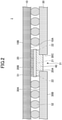
- Fig. 2 is a cross-sectional view illustrating an example of the semiconductor apparatus according to the first embodiment.
- Fig. 2 illustrates a cross-section taken along the line II-II in Fig. 1 .
- a semiconductor apparatus 1 of the first embodiment primarily includes an interconnect substrate 30, a first semiconductor device 10, a second semiconductor device 20, and a heatsink member 40.
- the interconnect substrate 30 has one major surface 30A and the other major surface 30B.
- the surface 30A may be referred to as an upper surface, and the surface 30B may be referred to as a lower surface.
- the side where the surface 30A is situated may be referred to as an upper side, and the side where the surface 30B is situated may be referred to as a lower side.
- the interconnect substrate 30 includes one or more interconnect layers (not shown) and one or more insulating layers (not shown) that are in contact with the respective interconnect layers in the thickness direction.
- a plurality of first electrode pads (not shown) are disposed on the major surface 30A of the interconnect substrate 30.
- the major surface 30A is an example of a first major surface.
- the major surface 30B of the interconnect substrate 30 may have electrode pads formed thereon, which may be connected to a motherboard or the like via solder balls or the like disposed on the electrode pads.
- the "plan view” refers to a view normal to the major surface 30A. It may be noted that the semiconductor apparatus 1 may be used in an upside-down position, or may be placed at any angle.
- the first semiconductor device 10 has one major surface 10A and the other major surface 10B.
- the major surface 10A faces downward, and the major surface 10B faces upward.
- the major surface 10A may be referred to as a lower surface, and the major surface 10B may be referred to as an upper surface.
- the major surface 10A opposes the major surface 30A of the interconnect substrate 30.
- a plurality of second electrode pads are disposed on the major surface 10A of the first semiconductor device 10 such as to oppose the first electrode pads on the interconnect substrate 30.
- the first electrode pads of the interconnect substrate 30 and the second electrode pads of the first semiconductor device 10 are connected to each other via respective conductive bumps 52.
- the conductive bumps 52 are solder bumps, gold bumps, copper bumps, or the like, for example.
- a plurality of third electrode pads (not shown), which are smaller than the second electrode pads, are also disposed on the major surface 10A of the first semiconductor device 10 in addition to the second electrode pads.
- the major surface 10A is an example of a second major surface.
- the second semiconductor device 20 has one major surface 20A and the other major surface 20B.
- the major surface 20A faces downward, and the major surface 20B faces upward.
- the major surface 20A may be referred to as a lower surface, and the major surface 20B may be referred to as an upper surface.
- the major surface 20A faces toward the major surface 30A of the interconnect substrate 30. and the major surface 20B opposes the major surface 10A of the first semiconductor device 10.
- a plurality of fourth electrode pads are disposed on the major surface 20B of the second semiconductor device 20 such as to oppose the third electrode pads on the first semiconductor device 10.
- the third electrode pads of the first semiconductor device 10 and the fourth electrode pads of the second semiconductor device 20 are connected to each other via respective conductive bumps 51.
- the conductive bumps 51 are solder bumps, gold bumps, copper bumps, or the like, for example.
- the major surface 20A is an example of a third major surface
- the major surface 20B is an example of a fourth major surface.
- a through hole 31 is formed through the interconnect substrate 30 at the position overlapping the second semiconductor device 20 in the plan view.
- the through hole 31 is situated inside the perimeter of the major surface 20A in the plan view.
- the heatsink member 40 is in contact with at least a part of the major surface 30A of the interconnect substrate 30, part of the major surface 20A of the second semiconductor device 20, and at least a part of a sidewall surface 30C of the through hole 31.
- the heatsink member 40 is situated inside the perimeter of the major surface 20A in the plan view.
- the major surface 20A of the second semiconductor device 20 includes a first area 21 and a second area 22 adjoining the first area 21.
- the heatsink member 40 is in contact with the first area 21, but is not in contact with the second area 22.
- the heatsink member 40 is partially in contact with the major surface 20A.
- the heatsink member 40 is inserted into the through hole 31, for example, and is made by curing a thermal interface material (TIM) paste.
- the heatsink member 40 may be made of an insulator such as a resin or alumina, a conductor such as a metal, graphene, or carbon nanotubes, or both an insulator and a conductor.
- heat generated by the first semiconductor device 10 is transferred to the interconnect substrate 30 mainly through the conductive bumps 52.
- the heat transferred to the interconnect substrate 30 spreads to the exterior surface of the interconnect substrate 30 such as the major surface 30B through the interconnect layers and the like of the interconnect substrate 30, followed by being dissipated to outside the semiconductor apparatus 1.
- the heat generated by the second semiconductor device 20 is mainly transferred to the heatsink member 40.
- the heat transferred to the heatsink member 40 is dissipated to outside, or is transmitted to the interconnect substrate 30.
- the heat transferred to the interconnect substrate 30 spreads to the exterior surface of the interconnect substrate 30 such as the major surface 30B through the interconnect layers and the like of the interconnect substrate 30, followed by being dissipated to outside the semiconductor apparatus 1.
- heat generated by the second semiconductor device 20 is not only dissipated to outside from the heatsink member 40, but also dissipated to outside through the interconnect substrate 30. Accordingly, heat is dissipated with higher efficiency than in the case in which a heatsink plate is only attached to the major surface 20A of the second semiconductor device 20 Further, this arrangement reduces the proportion of heat transferred to the first semiconductor device 10 in the total amount of heat generated by the second semiconductor device 20, thereby reducing a temperature increase in the first semiconductor device 10.
- An underfill may be disposed between the major surface 30A and the major surface 10A. In such a case, it is preferable for the heat conductivity of the heatsink member 40 to be higher than the heat conductivity of the underfill.
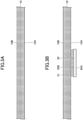
- FIGs. 3A and 3B through Fig. 5 are cross-sectional views illustrating the method of making the semiconductor apparatus according to the first embodiment.
- the first semiconductor device 10 having the major surface 10A and the major surface 10B is provided.
- a plurality of second electrode pads (not shown) to be connected to the interconnect substrate 30 and a plurality of third electrode pads (not shown) to be connected to the second semiconductor device are disposed on the major surface 10A.
- the second semiconductor device 20 is provided, and the second semiconductor device 20 is mounted to the first semiconductor device 10.
- the second semiconductor device 20 has the major surface 20A and the major surface 20B.
- a plurality of fourth electrode pads (not shown) to be connected to the third electrode pads on the first semiconductor device 10 are disposed on the major surface 20B.
- the second semiconductor device 20 is mounted such that the major surface 20B of the second semiconductor device 20 opposes the major surface 10A of the first semiconductor device 10 and such that the conductive bumps 51 are used to connect the fourth electrode pads of the second semiconductor device 20 to the third electrode pads of the first semiconductor device 10.
- the interconnect substrate 30 having the through hole 31 formed therethrough is provided, and the first semiconductor device 10 is mounted to the interconnect substrate 30.
- the interconnect substrate 30 has the major surface 30A and the major surface 30B.
- a plurality of first electrode pads (not shown) to be connected to the second electrode pads on the first semiconductor device 10 are disposed on the major surface 30A.
- the first semiconductor device 10 is mounted such that the major surface 10A of the first semiconductor device 10 opposes the major surface 30A of the interconnect substrate 30 and such that the conductive bumps 52 are used to connect the second electrode pads of the first semiconductor device 10 to the first electrode pads of the interconnect substrate 30.
- the through hole 31 is positioned inside the perimeter of the major surface 20A in the plan view.
- the heatsink member 40 is formed such as to be in contact with part of the major surface 30A of the interconnect substrate 30, part of the major surface 20A of the second semiconductor device 20, and at least a part of the sidewall surface 30C of the through hole 31.
- a TIM paste or the like is injected into the through hole 31, and is cured by application of heat.
- the TIM paste or the like contains either an insulator, a conductor, or both, for example.
- an underfill may be disposed between the major surface 30A and the major surface 10A.
- FIG. 6 is a cross-sectional view illustrating an example of a semiconductor apparatus according to the second embodiment.
- the major surface 20A of the second semiconductor device 20 includes the first area 21 in contact with the heatsink member 40 and the second area 22 adjoining the first area 21, and a wall 71 containing a resin is provided on the second area 22.
- the wall 71 is made of an epoxy resin, an acrylic resin, a silicone resin, or the like, for example.
- the second area 22 encloses the first area 21, so that the wall 71 formed on the major surface 20A has a loop shape extending along the outer perimeter of the second semiconductor device 20.
- the height of the wall 71 is preferably greater than or equal to 1/2 of the distance between the major surface 30A and the major surface 20A, more preferably greater than or equal to 2/3 thereof, and yet more preferably greater than or equal to 3/4 thereof.
- the wall 71 prevents the heatsink member 40 from coming in contact with the major surface 20A so that the heatsink member 40 is not in contact with the second area 22.
- the wall 71 is an example of a blocking mechanism.
- the remaining configurations are substantially the same as the configurations of the first embodiment.
- the flow of paste is limited by the wall 71 when a TIM paste or the like is injected into the through hole 31 when forming the heatsink member 40.
- wetting and spreading over the major surface 20A can be reduced.
- Reduction of wetting and spreading over the major surface 20A also serves to reduce wetting and spreading over the major surface 30A.
- Excessive spreading of paste creates the risk that the paste comes in contact with the conductive bumps 52.
- the paste coming in contact with the conductive bumps 52 may result in reducing the resistance of the conductive bumps 52 to thermal expansion.
- the paste has some electrical conductivity, there may be a risk of short-circuiting.
- excessive spreading of paste creates the risk that the reliability of the conductive bumps 52 is lowered.
- excessive spreading of paste is reduced, thereby reducing such lowering of reliability of the conductive bumps 52.
- the second embodiment also improves heat dissipation efficiency as in the case of the first embodiment.
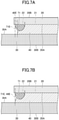
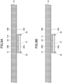
- FIGS. 7A and 7B are cross-sectional views illustrating examples of the shape of the heatsink member 40 according to the second embodiment.
- the outer edge 40E of the heatsink member 40 is situated inside the outer edge 71E of the wall 71 in the plan view.
- the outer edge 40E of the heatsink member 40 is aligned with the outer edge 71E of the wall 71 in the plan view.
- the outer edge 40E of the heatsink member 40 is preferably either aligned with the outer edge 71E of the wall 71 or situated inside the outer edge 71E of the wall 71 in the plan view.
- a TIM paste or the like used to form the heatsink member 40 flows along the surface of the wall 71 and the major surface 30A, so that the border between the surface of the heatsink member 40 and the surface of the wall 71 is likely to be situated inside the border between the surface of the heatsink member 40 and the major surface 30A.
- the lateral surface of the heatsink member 40 may be at an angle to the major surface 30A such as to flare outward toward the bottom at the major surface 30A.
- the lateral surface of the structure constituted by the heatsink member 40 and the wall 71 may be such that a recess is formed in the surface perpendicular to the major surface 30A.
- the outer edge of the interface between the heatsink member 40 and the second semiconductor device 20 may be situated inside the outer edge of the interface between the heatsink member 40 and the interconnect substrate 30.
- the outer edge 40E of the heatsink member 40 may be situated inside the outer edge of the second semiconductor device 20, for example.
- the plane shape of the wall 71 does not have to be a loop shape.
- the wall 71 may be formed only along three sides, or may be formed only along two sides parallel to each other.
- FIGS. 8A and 8B are cross-sectional views illustrating the method of making the semiconductor apparatus according to the second embodiment.
- the processes up to the mounting of the second semiconductor device 20 to the first semiconductor device 10 are performed (see Figs. 3A and 3B ).
- a dispenser or the like is used to deposit an uncured resin paste 71A on the second area 22 of the major surface 20A.
- the resin paste 71A is then heated and cured to form the wall 71 as illustrated in Fig. 8B .
- the processes at and after the mounting of the first semiconductor device 10 to the interconnect substrate 30 are performed (see Fig. 4 and Fig. 5 ).
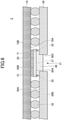
- FIG. 9 is a cross-sectional view illustrating an example of a semiconductor apparatus according to the third embodiment.
- a wall 72 containing metal is disposed in the second area 22, in place of the wall 71 of the second embodiment.
- the wall 72 is made of silver, copper, gold, or the like, for example.
- the height of the wall 72 is preferably greater than or equal to 1/2 of the distance between the major surface 30A and the major surface 20A, more preferably greater than or equal to 2/3 thereof, and yet more preferably greater than or equal to 3/4 thereof.
- the wall 72 prevents the heatsink member 40 from coming in contact with the major surface 20A so that the heatsink member 40 is not in contact with the second area 22.
- the wall 72 is an example of a blocking mechanism.
- the flow of paste is limited by the wall 72 when a TIM paste or the like is injected into the through hole 31 when forming the heatsink member 40.
- excessive spreading of paste is reduced, thereby reducing the lowering of reliability of the conductive bumps 52.
- the third embodiment also improves heat dissipation efficiency as in the case of the first embodiment.
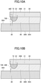
- FIGS. 10A and 10B are cross-sectional views illustrating examples of the shape of the heatsink member 40 according to the third embodiment.
- the outer edge 40E of the heatsink member 40 is situated inside the outer edge 72E of the wall 72 in the plan view.
- the outer edge 40E of the heatsink member 40 is aligned with the outer edge 72E of the wall 72 in the plan view. In this manner, the outer edge 40E of the heatsink member 40 is preferably either aligned with the outer edge 72E of the wall 72 or situated inside the outer edge 72E of the wall 72 in the plan view.
- a TIM paste or the like used to form the heatsink member 40 flows along the surface of the wall 72 and the major surface 30A, so that the border between the surface of the heatsink member 40 and the surface of the wall 72 is likely to be situated inside the border between the surface of the heatsink member 40 and the major surface 30A.
- the lateral surface of the heatsink member 40 may be at an angle to the major surface 30A such as to flare outward toward the bottom at the major surface 30A.
- the lateral surface of the structure constituted by the heatsink member 40 and the wall 72 may be such that a recess is formed in the surface perpendicular to the major surface 30A.
- the outer edge of the interface between the heatsink member 40 and the second semiconductor device 20 may be situated inside the outer edge of the interface between the heatsink member 40 and the interconnect substrate 30.
- the outer edge 40E of the heatsink member 40 may be situated inside the outer edge of the second semiconductor device 20, for example.
- a past containing metal may be used as the material of the wall 72, in place of a resin paste used as the material of the wall 71, for example.
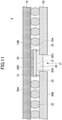
- FIG. 11 is a cross-sectional view illustrating an example of a semiconductor apparatus according to the fourth embodiment.
- neither the wall 71 of the second embodiment nor the wall 72 is provided in the second area 22, and the second area 22 is formed as a liquidphobic surface.
- the second area 22 may have been subjected to plasma processing or exposed to deep ultraviolet light.
- the liquidphobic surface prevents the heatsink member 40 from coming in contact with the major surface 20A so that the heatsink member 40 is not in contact with the second area 22.
- the liquidphobic surface is an example of a blocking mechanism.
- the lateral surface of the heatsink member 40 may be at an angle to the major surface 30A such as to flare outward toward the bottom at the major surface 30A.
- the flow of paste is limited by the liquidphobic surface of the second area 22 when a TIM paste or the like is injected into the through hole 31 when forming the heatsink member 40.
- excessive spreading of paste is reduced, thereby reducing the lowering of reliability of the conductive bumps 52.
- the fourth embodiment also improves heat dissipation efficiency as in the case of the first embodiment.
- Fig. 12 is a cross-sectional view illustrating an example of the shape of the heatsink member 40 according to the fourth embodiment.
- the lateral surface of the heatsink member 40 between the major surface 20A and the major surface 30A is at an angle to the major surface 30A such as to flare outward toward the bottom at the major surface 30A.
- the outer edge of the interface between the heatsink member 40 and the second semiconductor device 20 may be situated inside the outer edge of the interface between the heatsink member 40 and the interconnect substrate 30.
- the outer edge 40E of the heatsink member 40 may be situated inside the outer edge of the second semiconductor device 20, for example.
- neither the wall 71 nor the wall 72 is formed, and the second area 22 is subjected to plasma processing or exposed to deep ultraviolet light to be made into a liquidphobic surface, for example.
- FIG. 13 is a cross-sectional view illustrating an example of a semiconductor apparatus according to the fifth embodiment.
- a recess 23 is formed in the first area 21, and a bulge 24 adjoining the recess 23 is formed in the second area 22.
- the heatsink member 40 is in contact with the second semiconductor device 20 at the interior surface of the recess 23.
- the recess 23 is an example of a first recess, and the bulge 24 is part of the blocking mechanism.
- the remaining configurations are substantially the same as the configurations of the first embodiment.
- the flow of paste is limited by the bulge 24 when a TIM paste or the like is injected into the through hole 31 when forming the heatsink member 40.
- excessive spreading of paste is reduced, thereby reducing the lowering of reliability of the conductive bumps 52.
- the fifth embodiment also improves heat dissipation efficiency as in the case of the first embodiment.
- the shapes of the recess 23 and the bulge 24 are not limited to a particular shape.
- the bulge 24 may be formed in a loop shape.
- the bulge 24 may be formed only along two sides parallel to each other.
- the second semiconductor device 20 may be processed to have the recess 23 before being mounted to the first semiconductor device 10, for example.
- the recess 23 may be formed by dry etching or wet etching using an etching mask.
- a dicing saw may be used to form the recess 23 in conjunction with a dicing process before or after dicing the wafer.
- FIG. 14 is a cross-sectional view illustrating an example of a semiconductor apparatus according to the sixth embodiment.
- the interconnect substrate 30 has an external interconnect layer 33 that is exposed at the sidewall surface 30C of the through hole 31.
- the external interconnect layer 33 is electrically connected to one or more internal interconnect layers (not shown) such as a ground layer formed inside the interconnect substrate 30.
- the external interconnect layer 33 is disposed all over the sidewall surface 30C.
- the heatsink member 40 is in contact with at least a portion of the external interconnect layer 33.
- the external interconnect layer 33 contains copper or a copper alloy, for example.
- the remaining configurations are substantially the same as the configurations of the first embodiment.
- heat is transmitted from the heatsink member 40 to the interconnect substrate 30 through the external interconnect layer 33.
- the external interconnect layer 33 has higher thermal conductivity than the insulating layers. In the semiconductor apparatus 6, thus, heat is transmitted from the heatsink member 40 to the interconnect substrate 30 with increased efficiency.
- the interconnect substrate 30 may include an internal interconnect layer, such as a ground layer, having a relatively large area, and the external interconnect layer 33 may be connected to this internal interconnect layer. In such a case, heat is readily dissipated inside the interconnect substrate 30 at high speed, which achieves a further increased heat dissipation efficiency.
- the external interconnect layer 33 may be formed after forming the through hole 31 during the fabrication of the interconnect substrate 30, for example.
- FIG. 15 is a cross-sectional view illustrating an example of a semiconductor apparatus according to the seventh embodiment.
- the major surface 30A of the interconnect substrate 30 has a cavity 35 formed therein that continues from the through hole 31 and that is wider than the second semiconductor device 20 in the plan view.
- the major surface 20A of the second semiconductor device 20 is situated closer to the major surface 30B of the interconnect substrate 30 than is the upper end of the cavity 35.
- the bottom surface of the cavity 35 is part of the major surface 30A as defined in the present disclosures.
- the heatsink member 40 is in contact with at least a part of the bottom surface of the cavity 35, part of the major surface 20A of the second semiconductor device 20, and at least a part of the sidewall surface 30C of the through hole 31.
- the distance between the major surface 30A and the major surface 10A is less than that of the first embodiment. Accordingly, the height of the conductive bumps 52 is less than that of the first embodiment.
- the remaining configurations are substantially the same as the configurations of the first embodiment.
- the seventh embodiment also improves heat dissipation efficiency as in the case of the first embodiment. Further, the dimension of the semiconductor apparatus 7 of the seventh embodiment in the thickness direction is readily made smaller than that of the semiconductor apparatus 1 of the first embodiment.
- the cavity 35 may be formed during the fabrication of the interconnect substrate 30, for example.
- any one of the second through fourth embodiments maybe combined with the seventh embodiment.
- the fifth and/or sixth embodiments maybe combined with the seventh embodiment.
- heat dissipation efficiency is improved.
Landscapes
- Cooling Or The Like Of Semiconductors Or Solid State Devices (AREA)
- Wire Bonding (AREA)
- Chemical & Material Sciences (AREA)
- Engineering & Computer Science (AREA)
- Materials Engineering (AREA)
Applications Claiming Priority (1)
| Application Number | Priority Date | Filing Date | Title |
|---|---|---|---|
| JP2020141650A JP7510817B2 (ja) | 2020-08-25 | 2020-08-25 | 半導体装置及びその製造方法 |
Publications (1)
| Publication Number | Publication Date |
|---|---|
| EP3961702A1 true EP3961702A1 (de) | 2022-03-02 |
Family
ID=77465809
Family Applications (1)
| Application Number | Title | Priority Date | Filing Date |
|---|---|---|---|
| EP21192082.2A Pending EP3961702A1 (de) | 2020-08-25 | 2021-08-19 | Halbleitervorrichtung und dafür vorgesehenes herstellungsverfahren |
Country Status (3)
| Country | Link |
|---|---|
| US (1) | US11776903B2 (de) |
| EP (1) | EP3961702A1 (de) |
| JP (1) | JP7510817B2 (de) |
Citations (7)
| Publication number | Priority date | Publication date | Assignee | Title |
|---|---|---|---|---|
| US6265771B1 (en) * | 1999-01-27 | 2001-07-24 | International Business Machines Corporation | Dual chip with heat sink |
| JP2002359345A (ja) | 2001-03-30 | 2002-12-13 | Toshiba Corp | 半導体装置及びその製造方法 |
| US6759737B2 (en) * | 2000-03-25 | 2004-07-06 | Amkor Technology, Inc. | Semiconductor package including stacked chips with aligned input/output pads |
| US20080315398A1 (en) * | 2007-06-22 | 2008-12-25 | Hsing-Lun Lo | Packaging substrate with embedded chip and buried heatsink |
| US20120075807A1 (en) * | 2010-09-24 | 2012-03-29 | Gamal Refai-Ahmed | Stacked semiconductor chip device with thermal management |
| US20150255366A1 (en) * | 2014-03-06 | 2015-09-10 | Apple Inc. | Embedded system in package |
| US10515867B2 (en) * | 2017-11-14 | 2019-12-24 | Taiwan Semiconductor Manufacturing Company Ltd. | Semiconductor structure and manufacturing method thereof |
Family Cites Families (14)
| Publication number | Priority date | Publication date | Assignee | Title |
|---|---|---|---|---|
| JP3018554B2 (ja) * | 1991-04-25 | 2000-03-13 | 株式会社日立製作所 | 半導体モジュ−ル及びその製造方法 |
| US6815829B2 (en) | 2000-03-29 | 2004-11-09 | Rohm Co., Ltd. | Semiconductor device with compact package |
| US6791839B2 (en) | 2002-06-25 | 2004-09-14 | Dow Corning Corporation | Thermal interface materials and methods for their preparation and use |
| US7646093B2 (en) * | 2006-12-20 | 2010-01-12 | Intel Corporation | Thermal management of dies on a secondary side of a package |
| US20110163348A1 (en) * | 2008-03-25 | 2011-07-07 | Bridge Semiconductor Corporation | Semiconductor chip assembly with bump/base heat spreader and inverted cavity in bump |
| TWI357135B (en) * | 2008-05-29 | 2012-01-21 | Ind Tech Res Inst | Chip package structure and manufacturing method th |
| JP2011091266A (ja) | 2009-10-23 | 2011-05-06 | Panasonic Corp | 半導体装置およびその製造方法 |
| JP2012191002A (ja) | 2011-03-10 | 2012-10-04 | Panasonic Corp | 半導体装置 |
| US10008475B2 (en) | 2012-09-27 | 2018-06-26 | Intel Corporation | Stacked-die including a die in a package substrate |
| US9196575B1 (en) * | 2013-02-04 | 2015-11-24 | Altera Corporation | Integrated circuit package with cavity in substrate |
| JP6284193B2 (ja) | 2014-09-22 | 2018-02-28 | リボンディスプレイジャパン株式会社 | 電子部品の回路基板構造 |
| JP2017005029A (ja) | 2015-06-05 | 2017-01-05 | 日立金属株式会社 | 多層基板及びそれを用いた通信モジュール |
| US9768145B2 (en) | 2015-08-31 | 2017-09-19 | Taiwan Semiconductor Manufacturing Company, Ltd. | Methods of forming multi-die package structures including redistribution layers |
| US11574851B2 (en) * | 2019-02-27 | 2023-02-07 | Intel Corporation | Coupled cooling fins in ultra-small systems |
-
2020
- 2020-08-25 JP JP2020141650A patent/JP7510817B2/ja active Active
-
2021
- 2021-08-17 US US17/445,227 patent/US11776903B2/en active Active
- 2021-08-19 EP EP21192082.2A patent/EP3961702A1/de active Pending
Patent Citations (7)
| Publication number | Priority date | Publication date | Assignee | Title |
|---|---|---|---|---|
| US6265771B1 (en) * | 1999-01-27 | 2001-07-24 | International Business Machines Corporation | Dual chip with heat sink |
| US6759737B2 (en) * | 2000-03-25 | 2004-07-06 | Amkor Technology, Inc. | Semiconductor package including stacked chips with aligned input/output pads |
| JP2002359345A (ja) | 2001-03-30 | 2002-12-13 | Toshiba Corp | 半導体装置及びその製造方法 |
| US20080315398A1 (en) * | 2007-06-22 | 2008-12-25 | Hsing-Lun Lo | Packaging substrate with embedded chip and buried heatsink |
| US20120075807A1 (en) * | 2010-09-24 | 2012-03-29 | Gamal Refai-Ahmed | Stacked semiconductor chip device with thermal management |
| US20150255366A1 (en) * | 2014-03-06 | 2015-09-10 | Apple Inc. | Embedded system in package |
| US10515867B2 (en) * | 2017-11-14 | 2019-12-24 | Taiwan Semiconductor Manufacturing Company Ltd. | Semiconductor structure and manufacturing method thereof |
Also Published As
| Publication number | Publication date |
|---|---|
| JP7510817B2 (ja) | 2024-07-04 |
| US11776903B2 (en) | 2023-10-03 |
| JP2022037487A (ja) | 2022-03-09 |
| US20220068806A1 (en) | 2022-03-03 |
Similar Documents
| Publication | Publication Date | Title |
|---|---|---|
| CN213752684U (zh) | 具有竖直热管理的堆叠式硅封装组件 | |
| US10840219B2 (en) | Semiconductor package structure and method for manufacturing the same | |
| CN109256371B (zh) | 半导体封装结构及其形成方法 | |
| EP3567628B1 (de) | Halbleitergehäusesystem | |
| US9922902B2 (en) | Semiconductor device and semiconductor package | |
| US7196411B2 (en) | Heat dissipation for chip-on-chip IC packages | |
| US9460983B2 (en) | Joining structure using thermal interface material | |
| EP2664228B1 (de) | Vorrichtungen mit kühlkörpern mit anisotroper leitfähigkeit und herstellungsverfahren dafür | |
| US7772692B2 (en) | Semiconductor device with cooling member | |
| US6111313A (en) | Integrated circuit package having a stiffener dimensioned to receive heat transferred laterally from the integrated circuit | |
| US11387159B2 (en) | Chip package | |
| TWI543314B (zh) | 半導體封裝物 | |
| KR101069499B1 (ko) | 반도체 디바이스 및 그 제조 방법 | |
| US5889324A (en) | Package for a semiconductor device | |
| US10475733B2 (en) | Method and structures for heat dissipating interposers | |
| US20090267221A1 (en) | Semiconductor device | |
| US11127650B2 (en) | Semiconductor device package including thermal dissipation element and method of manufacturing the same | |
| US20240063087A1 (en) | Thermal and mechanical enhanced thermal module structure on heterogeneous packages and methods for forming the same | |
| US9666506B2 (en) | Heat spreader with wiring substrate for reduced thickness | |
| US9659844B2 (en) | Semiconductor die substrate with integral heat sink | |
| KR20050077866A (ko) | 열방출형 반도체 패키지 및 그 제조방법 | |
| US8183686B2 (en) | Semiconductor device | |
| CN119447039A (zh) | 电子封装件及其制法 | |
| US20250285934A1 (en) | Thermally-conductive crystalline pedestal for semiconductor device packages | |
| US11776903B2 (en) | Semiconductor apparatus and method of making the same |
Legal Events
| Date | Code | Title | Description |
|---|---|---|---|
| PUAI | Public reference made under article 153(3) epc to a published international application that has entered the european phase |
Free format text: ORIGINAL CODE: 0009012 |
|
| STAA | Information on the status of an ep patent application or granted ep patent |
Free format text: STATUS: THE APPLICATION HAS BEEN PUBLISHED |
|
| AK | Designated contracting states |
Kind code of ref document: A1 Designated state(s): AL AT BE BG CH CY CZ DE DK EE ES FI FR GB GR HR HU IE IS IT LI LT LU LV MC MK MT NL NO PL PT RO RS SE SI SK SM TR |
|
| STAA | Information on the status of an ep patent application or granted ep patent |
Free format text: STATUS: REQUEST FOR EXAMINATION WAS MADE |
|
| 17P | Request for examination filed |
Effective date: 20220513 |
|
| RBV | Designated contracting states (corrected) |
Designated state(s): AL AT BE BG CH CY CZ DE DK EE ES FI FR GB GR HR HU IE IS IT LI LT LU LV MC MK MT NL NO PL PT RO RS SE SI SK SM TR |