EP3958304A2 - Gehäusestruktur und verfahren zur formung davon - Google Patents
Gehäusestruktur und verfahren zur formung davon Download PDFInfo
- Publication number
- EP3958304A2 EP3958304A2 EP21188007.5A EP21188007A EP3958304A2 EP 3958304 A2 EP3958304 A2 EP 3958304A2 EP 21188007 A EP21188007 A EP 21188007A EP 3958304 A2 EP3958304 A2 EP 3958304A2
- Authority
- EP
- European Patent Office
- Prior art keywords
- die
- tim
- package structure
- adhesive pattern
- dies
- Prior art date
- Legal status (The legal status is an assumption and is not a legal conclusion. Google has not performed a legal analysis and makes no representation as to the accuracy of the status listed.)
- Withdrawn
Links
Images






Classifications
-
- H—ELECTRICITY
- H10—SEMICONDUCTOR DEVICES; ELECTRIC SOLID-STATE DEVICES NOT OTHERWISE PROVIDED FOR
- H10W—GENERIC PACKAGES, INTERCONNECTIONS, CONNECTORS OR OTHER CONSTRUCTIONAL DETAILS OF DEVICES COVERED BY CLASS H10
- H10W74/00—Encapsulations, e.g. protective coatings
- H10W74/10—Encapsulations, e.g. protective coatings characterised by their shape or disposition
- H10W74/111—Encapsulations, e.g. protective coatings characterised by their shape or disposition the semiconductor body being completely enclosed
- H10W74/114—Encapsulations, e.g. protective coatings characterised by their shape or disposition the semiconductor body being completely enclosed by a substrate and the encapsulations
- H10W74/117—Encapsulations, e.g. protective coatings characterised by their shape or disposition the semiconductor body being completely enclosed by a substrate and the encapsulations the substrate having spherical bumps for external connection
-
- H—ELECTRICITY
- H10—SEMICONDUCTOR DEVICES; ELECTRIC SOLID-STATE DEVICES NOT OTHERWISE PROVIDED FOR
- H10D—INORGANIC ELECTRIC SEMICONDUCTOR DEVICES
- H10D88/00—Three-dimensional [3D] integrated devices
-
- H—ELECTRICITY
- H10—SEMICONDUCTOR DEVICES; ELECTRIC SOLID-STATE DEVICES NOT OTHERWISE PROVIDED FOR
- H10W—GENERIC PACKAGES, INTERCONNECTIONS, CONNECTORS OR OTHER CONSTRUCTIONAL DETAILS OF DEVICES COVERED BY CLASS H10
- H10W40/00—Arrangements for thermal protection or thermal control
- H10W40/20—Arrangements for cooling
- H10W40/22—Arrangements for cooling characterised by their shape, e.g. having conical or cylindrical projections
-
- H—ELECTRICITY
- H10—SEMICONDUCTOR DEVICES; ELECTRIC SOLID-STATE DEVICES NOT OTHERWISE PROVIDED FOR
- H10W—GENERIC PACKAGES, INTERCONNECTIONS, CONNECTORS OR OTHER CONSTRUCTIONAL DETAILS OF DEVICES COVERED BY CLASS H10
- H10W40/00—Arrangements for thermal protection or thermal control
- H10W40/20—Arrangements for cooling
- H10W40/25—Arrangements for cooling characterised by their materials
- H10W40/251—Organics
-
- H—ELECTRICITY
- H10—SEMICONDUCTOR DEVICES; ELECTRIC SOLID-STATE DEVICES NOT OTHERWISE PROVIDED FOR
- H10W—GENERIC PACKAGES, INTERCONNECTIONS, CONNECTORS OR OTHER CONSTRUCTIONAL DETAILS OF DEVICES COVERED BY CLASS H10
- H10W40/00—Arrangements for thermal protection or thermal control
- H10W40/70—Fillings or auxiliary members in containers or in encapsulations for thermal protection or control
-
- H—ELECTRICITY
- H10—SEMICONDUCTOR DEVICES; ELECTRIC SOLID-STATE DEVICES NOT OTHERWISE PROVIDED FOR
- H10W—GENERIC PACKAGES, INTERCONNECTIONS, CONNECTORS OR OTHER CONSTRUCTIONAL DETAILS OF DEVICES COVERED BY CLASS H10
- H10W70/00—Package substrates; Interposers; Redistribution layers [RDL]
- H10W70/60—Insulating or insulated package substrates; Interposers; Redistribution layers
- H10W70/62—Insulating or insulated package substrates; Interposers; Redistribution layers characterised by their interconnections
- H10W70/65—Shapes or dispositions of interconnections
-
- H—ELECTRICITY
- H10—SEMICONDUCTOR DEVICES; ELECTRIC SOLID-STATE DEVICES NOT OTHERWISE PROVIDED FOR
- H10W—GENERIC PACKAGES, INTERCONNECTIONS, CONNECTORS OR OTHER CONSTRUCTIONAL DETAILS OF DEVICES COVERED BY CLASS H10
- H10W72/00—Interconnections or connectors in packages
- H10W72/01—Manufacture or treatment
- H10W72/013—Manufacture or treatment of die-attach connectors
-
- H—ELECTRICITY
- H10—SEMICONDUCTOR DEVICES; ELECTRIC SOLID-STATE DEVICES NOT OTHERWISE PROVIDED FOR
- H10W—GENERIC PACKAGES, INTERCONNECTIONS, CONNECTORS OR OTHER CONSTRUCTIONAL DETAILS OF DEVICES COVERED BY CLASS H10
- H10W72/00—Interconnections or connectors in packages
- H10W72/20—Bump connectors, e.g. solder bumps or copper pillars; Dummy bumps; Thermal bumps
-
- H—ELECTRICITY
- H10—SEMICONDUCTOR DEVICES; ELECTRIC SOLID-STATE DEVICES NOT OTHERWISE PROVIDED FOR
- H10W—GENERIC PACKAGES, INTERCONNECTIONS, CONNECTORS OR OTHER CONSTRUCTIONAL DETAILS OF DEVICES COVERED BY CLASS H10
- H10W74/00—Encapsulations, e.g. protective coatings
- H10W74/01—Manufacture or treatment
-
- H—ELECTRICITY
- H10—SEMICONDUCTOR DEVICES; ELECTRIC SOLID-STATE DEVICES NOT OTHERWISE PROVIDED FOR
- H10W—GENERIC PACKAGES, INTERCONNECTIONS, CONNECTORS OR OTHER CONSTRUCTIONAL DETAILS OF DEVICES COVERED BY CLASS H10
- H10W74/00—Encapsulations, e.g. protective coatings
- H10W74/01—Manufacture or treatment
- H10W74/012—Manufacture or treatment of encapsulations on active surfaces of flip-chip devices, e.g. forming underfills
-
- H—ELECTRICITY
- H10—SEMICONDUCTOR DEVICES; ELECTRIC SOLID-STATE DEVICES NOT OTHERWISE PROVIDED FOR
- H10W—GENERIC PACKAGES, INTERCONNECTIONS, CONNECTORS OR OTHER CONSTRUCTIONAL DETAILS OF DEVICES COVERED BY CLASS H10
- H10W74/00—Encapsulations, e.g. protective coatings
- H10W74/01—Manufacture or treatment
- H10W74/016—Manufacture or treatment using moulds
-
- H—ELECTRICITY
- H10—SEMICONDUCTOR DEVICES; ELECTRIC SOLID-STATE DEVICES NOT OTHERWISE PROVIDED FOR
- H10W—GENERIC PACKAGES, INTERCONNECTIONS, CONNECTORS OR OTHER CONSTRUCTIONAL DETAILS OF DEVICES COVERED BY CLASS H10
- H10W74/00—Encapsulations, e.g. protective coatings
- H10W74/10—Encapsulations, e.g. protective coatings characterised by their shape or disposition
- H10W74/111—Encapsulations, e.g. protective coatings characterised by their shape or disposition the semiconductor body being completely enclosed
- H10W74/121—Encapsulations, e.g. protective coatings characterised by their shape or disposition the semiconductor body being completely enclosed by multiple encapsulations, e.g. by a thin protective coating and a thick encapsulation
-
- H—ELECTRICITY
- H10—SEMICONDUCTOR DEVICES; ELECTRIC SOLID-STATE DEVICES NOT OTHERWISE PROVIDED FOR
- H10W—GENERIC PACKAGES, INTERCONNECTIONS, CONNECTORS OR OTHER CONSTRUCTIONAL DETAILS OF DEVICES COVERED BY CLASS H10
- H10W74/00—Encapsulations, e.g. protective coatings
- H10W74/10—Encapsulations, e.g. protective coatings characterised by their shape or disposition
- H10W74/111—Encapsulations, e.g. protective coatings characterised by their shape or disposition the semiconductor body being completely enclosed
- H10W74/127—Encapsulations, e.g. protective coatings characterised by their shape or disposition the semiconductor body being completely enclosed characterised by arrangements for sealing or adhesion
-
- H—ELECTRICITY
- H10—SEMICONDUCTOR DEVICES; ELECTRIC SOLID-STATE DEVICES NOT OTHERWISE PROVIDED FOR
- H10W—GENERIC PACKAGES, INTERCONNECTIONS, CONNECTORS OR OTHER CONSTRUCTIONAL DETAILS OF DEVICES COVERED BY CLASS H10
- H10W74/00—Encapsulations, e.g. protective coatings
- H10W74/10—Encapsulations, e.g. protective coatings characterised by their shape or disposition
- H10W74/111—Encapsulations, e.g. protective coatings characterised by their shape or disposition the semiconductor body being completely enclosed
- H10W74/129—Encapsulations, e.g. protective coatings characterised by their shape or disposition the semiconductor body being completely enclosed forming a chip-scale package [CSP]
-
- H—ELECTRICITY
- H10—SEMICONDUCTOR DEVICES; ELECTRIC SOLID-STATE DEVICES NOT OTHERWISE PROVIDED FOR
- H10W—GENERIC PACKAGES, INTERCONNECTIONS, CONNECTORS OR OTHER CONSTRUCTIONAL DETAILS OF DEVICES COVERED BY CLASS H10
- H10W74/00—Encapsulations, e.g. protective coatings
- H10W74/10—Encapsulations, e.g. protective coatings characterised by their shape or disposition
- H10W74/131—Encapsulations, e.g. protective coatings characterised by their shape or disposition the semiconductor body being only partially enclosed
-
- H—ELECTRICITY
- H10—SEMICONDUCTOR DEVICES; ELECTRIC SOLID-STATE DEVICES NOT OTHERWISE PROVIDED FOR
- H10W—GENERIC PACKAGES, INTERCONNECTIONS, CONNECTORS OR OTHER CONSTRUCTIONAL DETAILS OF DEVICES COVERED BY CLASS H10
- H10W74/00—Encapsulations, e.g. protective coatings
- H10W74/10—Encapsulations, e.g. protective coatings characterised by their shape or disposition
- H10W74/131—Encapsulations, e.g. protective coatings characterised by their shape or disposition the semiconductor body being only partially enclosed
- H10W74/141—Encapsulations, e.g. protective coatings characterised by their shape or disposition the semiconductor body being only partially enclosed the encapsulations being on at least the sidewalls of the semiconductor body
-
- H—ELECTRICITY
- H10—SEMICONDUCTOR DEVICES; ELECTRIC SOLID-STATE DEVICES NOT OTHERWISE PROVIDED FOR
- H10W—GENERIC PACKAGES, INTERCONNECTIONS, CONNECTORS OR OTHER CONSTRUCTIONAL DETAILS OF DEVICES COVERED BY CLASS H10
- H10W74/00—Encapsulations, e.g. protective coatings
- H10W74/10—Encapsulations, e.g. protective coatings characterised by their shape or disposition
- H10W74/15—Encapsulations, e.g. protective coatings characterised by their shape or disposition on active surfaces of flip-chip devices, e.g. underfills
-
- H—ELECTRICITY
- H10—SEMICONDUCTOR DEVICES; ELECTRIC SOLID-STATE DEVICES NOT OTHERWISE PROVIDED FOR
- H10W—GENERIC PACKAGES, INTERCONNECTIONS, CONNECTORS OR OTHER CONSTRUCTIONAL DETAILS OF DEVICES COVERED BY CLASS H10
- H10W76/00—Containers; Fillings or auxiliary members therefor; Seals
- H10W76/10—Containers or parts thereof
- H10W76/12—Containers or parts thereof characterised by their shape
-
- H—ELECTRICITY
- H10—SEMICONDUCTOR DEVICES; ELECTRIC SOLID-STATE DEVICES NOT OTHERWISE PROVIDED FOR
- H10W—GENERIC PACKAGES, INTERCONNECTIONS, CONNECTORS OR OTHER CONSTRUCTIONAL DETAILS OF DEVICES COVERED BY CLASS H10
- H10W90/00—Package configurations
-
- H—ELECTRICITY
- H10—SEMICONDUCTOR DEVICES; ELECTRIC SOLID-STATE DEVICES NOT OTHERWISE PROVIDED FOR
- H10W—GENERIC PACKAGES, INTERCONNECTIONS, CONNECTORS OR OTHER CONSTRUCTIONAL DETAILS OF DEVICES COVERED BY CLASS H10
- H10W95/00—Packaging processes not covered by the other groups of this subclass
-
- H—ELECTRICITY
- H10—SEMICONDUCTOR DEVICES; ELECTRIC SOLID-STATE DEVICES NOT OTHERWISE PROVIDED FOR
- H10W—GENERIC PACKAGES, INTERCONNECTIONS, CONNECTORS OR OTHER CONSTRUCTIONAL DETAILS OF DEVICES COVERED BY CLASS H10
- H10W70/00—Package substrates; Interposers; Redistribution layers [RDL]
- H10W70/60—Insulating or insulated package substrates; Interposers; Redistribution layers
- H10W70/611—Insulating or insulated package substrates; Interposers; Redistribution layers for connecting multiple chips together
-
- H—ELECTRICITY
- H10—SEMICONDUCTOR DEVICES; ELECTRIC SOLID-STATE DEVICES NOT OTHERWISE PROVIDED FOR
- H10W—GENERIC PACKAGES, INTERCONNECTIONS, CONNECTORS OR OTHER CONSTRUCTIONAL DETAILS OF DEVICES COVERED BY CLASS H10
- H10W70/00—Package substrates; Interposers; Redistribution layers [RDL]
- H10W70/60—Insulating or insulated package substrates; Interposers; Redistribution layers
- H10W70/62—Insulating or insulated package substrates; Interposers; Redistribution layers characterised by their interconnections
- H10W70/63—Vias, e.g. via plugs
- H10W70/635—Through-vias
-
- H—ELECTRICITY
- H10—SEMICONDUCTOR DEVICES; ELECTRIC SOLID-STATE DEVICES NOT OTHERWISE PROVIDED FOR
- H10W—GENERIC PACKAGES, INTERCONNECTIONS, CONNECTORS OR OTHER CONSTRUCTIONAL DETAILS OF DEVICES COVERED BY CLASS H10
- H10W72/00—Interconnections or connectors in packages
-
- H—ELECTRICITY
- H10—SEMICONDUCTOR DEVICES; ELECTRIC SOLID-STATE DEVICES NOT OTHERWISE PROVIDED FOR
- H10W—GENERIC PACKAGES, INTERCONNECTIONS, CONNECTORS OR OTHER CONSTRUCTIONAL DETAILS OF DEVICES COVERED BY CLASS H10
- H10W72/00—Interconnections or connectors in packages
- H10W72/01—Manufacture or treatment
- H10W72/0198—Manufacture or treatment batch processes
-
- H—ELECTRICITY
- H10—SEMICONDUCTOR DEVICES; ELECTRIC SOLID-STATE DEVICES NOT OTHERWISE PROVIDED FOR
- H10W—GENERIC PACKAGES, INTERCONNECTIONS, CONNECTORS OR OTHER CONSTRUCTIONAL DETAILS OF DEVICES COVERED BY CLASS H10
- H10W72/00—Interconnections or connectors in packages
- H10W72/071—Connecting or disconnecting
- H10W72/072—Connecting or disconnecting of bump connectors
-
- H—ELECTRICITY
- H10—SEMICONDUCTOR DEVICES; ELECTRIC SOLID-STATE DEVICES NOT OTHERWISE PROVIDED FOR
- H10W—GENERIC PACKAGES, INTERCONNECTIONS, CONNECTORS OR OTHER CONSTRUCTIONAL DETAILS OF DEVICES COVERED BY CLASS H10
- H10W72/00—Interconnections or connectors in packages
- H10W72/071—Connecting or disconnecting
- H10W72/073—Connecting or disconnecting of die-attach connectors
-
- H—ELECTRICITY
- H10—SEMICONDUCTOR DEVICES; ELECTRIC SOLID-STATE DEVICES NOT OTHERWISE PROVIDED FOR
- H10W—GENERIC PACKAGES, INTERCONNECTIONS, CONNECTORS OR OTHER CONSTRUCTIONAL DETAILS OF DEVICES COVERED BY CLASS H10
- H10W72/00—Interconnections or connectors in packages
- H10W72/071—Connecting or disconnecting
- H10W72/073—Connecting or disconnecting of die-attach connectors
- H10W72/07351—Connecting or disconnecting of die-attach connectors characterised by changes in properties of the die-attach connectors during connecting
- H10W72/07354—Connecting or disconnecting of die-attach connectors characterised by changes in properties of the die-attach connectors during connecting changes in dispositions
-
- H—ELECTRICITY
- H10—SEMICONDUCTOR DEVICES; ELECTRIC SOLID-STATE DEVICES NOT OTHERWISE PROVIDED FOR
- H10W—GENERIC PACKAGES, INTERCONNECTIONS, CONNECTORS OR OTHER CONSTRUCTIONAL DETAILS OF DEVICES COVERED BY CLASS H10
- H10W72/00—Interconnections or connectors in packages
- H10W72/20—Bump connectors, e.g. solder bumps or copper pillars; Dummy bumps; Thermal bumps
- H10W72/251—Materials
- H10W72/252—Materials comprising solid metals or solid metalloids, e.g. PbSn, Ag or Cu
-
- H—ELECTRICITY
- H10—SEMICONDUCTOR DEVICES; ELECTRIC SOLID-STATE DEVICES NOT OTHERWISE PROVIDED FOR
- H10W—GENERIC PACKAGES, INTERCONNECTIONS, CONNECTORS OR OTHER CONSTRUCTIONAL DETAILS OF DEVICES COVERED BY CLASS H10
- H10W72/00—Interconnections or connectors in packages
- H10W72/20—Bump connectors, e.g. solder bumps or copper pillars; Dummy bumps; Thermal bumps
- H10W72/29—Bond pads specially adapted therefor
-
- H—ELECTRICITY
- H10—SEMICONDUCTOR DEVICES; ELECTRIC SOLID-STATE DEVICES NOT OTHERWISE PROVIDED FOR
- H10W—GENERIC PACKAGES, INTERCONNECTIONS, CONNECTORS OR OTHER CONSTRUCTIONAL DETAILS OF DEVICES COVERED BY CLASS H10
- H10W72/00—Interconnections or connectors in packages
- H10W72/30—Die-attach connectors
- H10W72/321—Structures or relative sizes of die-attach connectors
-
- H—ELECTRICITY
- H10—SEMICONDUCTOR DEVICES; ELECTRIC SOLID-STATE DEVICES NOT OTHERWISE PROVIDED FOR
- H10W—GENERIC PACKAGES, INTERCONNECTIONS, CONNECTORS OR OTHER CONSTRUCTIONAL DETAILS OF DEVICES COVERED BY CLASS H10
- H10W72/00—Interconnections or connectors in packages
- H10W72/30—Die-attach connectors
- H10W72/321—Structures or relative sizes of die-attach connectors
- H10W72/322—Multilayered die-attach connectors, e.g. a coating on a top surface of a core
- H10W72/323—Multilayered die-attach connectors, e.g. a coating on a top surface of a core characterised by the structures of the outermost layers, e.g. multilayered coatings
-
- H—ELECTRICITY
- H10—SEMICONDUCTOR DEVICES; ELECTRIC SOLID-STATE DEVICES NOT OTHERWISE PROVIDED FOR
- H10W—GENERIC PACKAGES, INTERCONNECTIONS, CONNECTORS OR OTHER CONSTRUCTIONAL DETAILS OF DEVICES COVERED BY CLASS H10
- H10W72/00—Interconnections or connectors in packages
- H10W72/30—Die-attach connectors
- H10W72/321—Structures or relative sizes of die-attach connectors
- H10W72/325—Die-attach connectors having a filler embedded in a matrix
-
- H—ELECTRICITY
- H10—SEMICONDUCTOR DEVICES; ELECTRIC SOLID-STATE DEVICES NOT OTHERWISE PROVIDED FOR
- H10W—GENERIC PACKAGES, INTERCONNECTIONS, CONNECTORS OR OTHER CONSTRUCTIONAL DETAILS OF DEVICES COVERED BY CLASS H10
- H10W72/00—Interconnections or connectors in packages
- H10W72/30—Die-attach connectors
- H10W72/331—Shapes of die-attach connectors
- H10W72/334—Cross-sectional shape, i.e. in side view
-
- H—ELECTRICITY
- H10—SEMICONDUCTOR DEVICES; ELECTRIC SOLID-STATE DEVICES NOT OTHERWISE PROVIDED FOR
- H10W—GENERIC PACKAGES, INTERCONNECTIONS, CONNECTORS OR OTHER CONSTRUCTIONAL DETAILS OF DEVICES COVERED BY CLASS H10
- H10W72/00—Interconnections or connectors in packages
- H10W72/30—Die-attach connectors
- H10W72/341—Dispositions of die-attach connectors, e.g. layouts
-
- H—ELECTRICITY
- H10—SEMICONDUCTOR DEVICES; ELECTRIC SOLID-STATE DEVICES NOT OTHERWISE PROVIDED FOR
- H10W—GENERIC PACKAGES, INTERCONNECTIONS, CONNECTORS OR OTHER CONSTRUCTIONAL DETAILS OF DEVICES COVERED BY CLASS H10
- H10W72/00—Interconnections or connectors in packages
- H10W72/30—Die-attach connectors
- H10W72/341—Dispositions of die-attach connectors, e.g. layouts
- H10W72/347—Dispositions of multiple die-attach connectors
-
- H—ELECTRICITY
- H10—SEMICONDUCTOR DEVICES; ELECTRIC SOLID-STATE DEVICES NOT OTHERWISE PROVIDED FOR
- H10W—GENERIC PACKAGES, INTERCONNECTIONS, CONNECTORS OR OTHER CONSTRUCTIONAL DETAILS OF DEVICES COVERED BY CLASS H10
- H10W72/00—Interconnections or connectors in packages
- H10W72/30—Die-attach connectors
- H10W72/351—Materials of die-attach connectors
-
- H—ELECTRICITY
- H10—SEMICONDUCTOR DEVICES; ELECTRIC SOLID-STATE DEVICES NOT OTHERWISE PROVIDED FOR
- H10W—GENERIC PACKAGES, INTERCONNECTIONS, CONNECTORS OR OTHER CONSTRUCTIONAL DETAILS OF DEVICES COVERED BY CLASS H10
- H10W72/00—Interconnections or connectors in packages
- H10W72/30—Die-attach connectors
- H10W72/351—Materials of die-attach connectors
- H10W72/352—Materials of die-attach connectors comprising metals or metalloids, e.g. solders
-
- H—ELECTRICITY
- H10—SEMICONDUCTOR DEVICES; ELECTRIC SOLID-STATE DEVICES NOT OTHERWISE PROVIDED FOR
- H10W—GENERIC PACKAGES, INTERCONNECTIONS, CONNECTORS OR OTHER CONSTRUCTIONAL DETAILS OF DEVICES COVERED BY CLASS H10
- H10W72/00—Interconnections or connectors in packages
- H10W72/30—Die-attach connectors
- H10W72/351—Materials of die-attach connectors
- H10W72/353—Materials of die-attach connectors not comprising solid metals or solid metalloids, e.g. ceramics
-
- H—ELECTRICITY
- H10—SEMICONDUCTOR DEVICES; ELECTRIC SOLID-STATE DEVICES NOT OTHERWISE PROVIDED FOR
- H10W—GENERIC PACKAGES, INTERCONNECTIONS, CONNECTORS OR OTHER CONSTRUCTIONAL DETAILS OF DEVICES COVERED BY CLASS H10
- H10W72/00—Interconnections or connectors in packages
- H10W72/30—Die-attach connectors
- H10W72/351—Materials of die-attach connectors
- H10W72/353—Materials of die-attach connectors not comprising solid metals or solid metalloids, e.g. ceramics
- H10W72/354—Materials of die-attach connectors not comprising solid metals or solid metalloids, e.g. ceramics comprising polymers
-
- H—ELECTRICITY
- H10—SEMICONDUCTOR DEVICES; ELECTRIC SOLID-STATE DEVICES NOT OTHERWISE PROVIDED FOR
- H10W—GENERIC PACKAGES, INTERCONNECTIONS, CONNECTORS OR OTHER CONSTRUCTIONAL DETAILS OF DEVICES COVERED BY CLASS H10
- H10W72/00—Interconnections or connectors in packages
- H10W72/50—Bond wires
- H10W72/59—Bond pads specially adapted therefor
-
- H—ELECTRICITY
- H10—SEMICONDUCTOR DEVICES; ELECTRIC SOLID-STATE DEVICES NOT OTHERWISE PROVIDED FOR
- H10W—GENERIC PACKAGES, INTERCONNECTIONS, CONNECTORS OR OTHER CONSTRUCTIONAL DETAILS OF DEVICES COVERED BY CLASS H10
- H10W72/00—Interconnections or connectors in packages
- H10W72/851—Dispositions of multiple connectors or interconnections
- H10W72/874—On different surfaces
- H10W72/877—Bump connectors and die-attach connectors
-
- H—ELECTRICITY
- H10—SEMICONDUCTOR DEVICES; ELECTRIC SOLID-STATE DEVICES NOT OTHERWISE PROVIDED FOR
- H10W—GENERIC PACKAGES, INTERCONNECTIONS, CONNECTORS OR OTHER CONSTRUCTIONAL DETAILS OF DEVICES COVERED BY CLASS H10
- H10W72/00—Interconnections or connectors in packages
- H10W72/90—Bond pads, in general
- H10W72/931—Shapes of bond pads
-
- H—ELECTRICITY
- H10—SEMICONDUCTOR DEVICES; ELECTRIC SOLID-STATE DEVICES NOT OTHERWISE PROVIDED FOR
- H10W—GENERIC PACKAGES, INTERCONNECTIONS, CONNECTORS OR OTHER CONSTRUCTIONAL DETAILS OF DEVICES COVERED BY CLASS H10
- H10W72/00—Interconnections or connectors in packages
- H10W72/90—Bond pads, in general
- H10W72/941—Dispositions of bond pads
- H10W72/9413—Dispositions of bond pads on encapsulations
-
- H—ELECTRICITY
- H10—SEMICONDUCTOR DEVICES; ELECTRIC SOLID-STATE DEVICES NOT OTHERWISE PROVIDED FOR
- H10W—GENERIC PACKAGES, INTERCONNECTIONS, CONNECTORS OR OTHER CONSTRUCTIONAL DETAILS OF DEVICES COVERED BY CLASS H10
- H10W72/00—Interconnections or connectors in packages
- H10W72/90—Bond pads, in general
- H10W72/951—Materials of bond pads
- H10W72/952—Materials of bond pads comprising metals or metalloids, e.g. PbSn, Ag or Cu
-
- H—ELECTRICITY
- H10—SEMICONDUCTOR DEVICES; ELECTRIC SOLID-STATE DEVICES NOT OTHERWISE PROVIDED FOR
- H10W—GENERIC PACKAGES, INTERCONNECTIONS, CONNECTORS OR OTHER CONSTRUCTIONAL DETAILS OF DEVICES COVERED BY CLASS H10
- H10W72/00—Interconnections or connectors in packages
- H10W72/90—Bond pads, in general
- H10W72/951—Materials of bond pads
- H10W72/953—Materials of bond pads not comprising solid metals or solid metalloids, e.g. polymers, ceramics or liquids
-
- H—ELECTRICITY
- H10—SEMICONDUCTOR DEVICES; ELECTRIC SOLID-STATE DEVICES NOT OTHERWISE PROVIDED FOR
- H10W—GENERIC PACKAGES, INTERCONNECTIONS, CONNECTORS OR OTHER CONSTRUCTIONAL DETAILS OF DEVICES COVERED BY CLASS H10
- H10W74/00—Encapsulations, e.g. protective coatings
-
- H—ELECTRICITY
- H10—SEMICONDUCTOR DEVICES; ELECTRIC SOLID-STATE DEVICES NOT OTHERWISE PROVIDED FOR
- H10W—GENERIC PACKAGES, INTERCONNECTIONS, CONNECTORS OR OTHER CONSTRUCTIONAL DETAILS OF DEVICES COVERED BY CLASS H10
- H10W74/00—Encapsulations, e.g. protective coatings
- H10W74/10—Encapsulations, e.g. protective coatings characterised by their shape or disposition
- H10W74/131—Encapsulations, e.g. protective coatings characterised by their shape or disposition the semiconductor body being only partially enclosed
- H10W74/142—Encapsulations, e.g. protective coatings characterised by their shape or disposition the semiconductor body being only partially enclosed the encapsulations exposing the passive side of the semiconductor body
-
- H—ELECTRICITY
- H10—SEMICONDUCTOR DEVICES; ELECTRIC SOLID-STATE DEVICES NOT OTHERWISE PROVIDED FOR
- H10W—GENERIC PACKAGES, INTERCONNECTIONS, CONNECTORS OR OTHER CONSTRUCTIONAL DETAILS OF DEVICES COVERED BY CLASS H10
- H10W90/00—Package configurations
- H10W90/401—Package configurations characterised by multiple insulating or insulated package substrates, interposers or RDLs
-
- H—ELECTRICITY
- H10—SEMICONDUCTOR DEVICES; ELECTRIC SOLID-STATE DEVICES NOT OTHERWISE PROVIDED FOR
- H10W—GENERIC PACKAGES, INTERCONNECTIONS, CONNECTORS OR OTHER CONSTRUCTIONAL DETAILS OF DEVICES COVERED BY CLASS H10
- H10W90/00—Package configurations
- H10W90/701—Package configurations characterised by the relative positions of pads or connectors relative to package parts
-
- H—ELECTRICITY
- H10—SEMICONDUCTOR DEVICES; ELECTRIC SOLID-STATE DEVICES NOT OTHERWISE PROVIDED FOR
- H10W—GENERIC PACKAGES, INTERCONNECTIONS, CONNECTORS OR OTHER CONSTRUCTIONAL DETAILS OF DEVICES COVERED BY CLASS H10
- H10W90/00—Package configurations
- H10W90/701—Package configurations characterised by the relative positions of pads or connectors relative to package parts
- H10W90/721—Package configurations characterised by the relative positions of pads or connectors relative to package parts of bump connectors
- H10W90/724—Package configurations characterised by the relative positions of pads or connectors relative to package parts of bump connectors between a chip and a stacked insulating package substrate, interposer or RDL
-
- H—ELECTRICITY
- H10—SEMICONDUCTOR DEVICES; ELECTRIC SOLID-STATE DEVICES NOT OTHERWISE PROVIDED FOR
- H10W—GENERIC PACKAGES, INTERCONNECTIONS, CONNECTORS OR OTHER CONSTRUCTIONAL DETAILS OF DEVICES COVERED BY CLASS H10
- H10W90/00—Package configurations
- H10W90/701—Package configurations characterised by the relative positions of pads or connectors relative to package parts
- H10W90/731—Package configurations characterised by the relative positions of pads or connectors relative to package parts of die-attach connectors
- H10W90/734—Package configurations characterised by the relative positions of pads or connectors relative to package parts of die-attach connectors between a chip and a stacked insulating package substrate, interposer or RDL
-
- H—ELECTRICITY
- H10—SEMICONDUCTOR DEVICES; ELECTRIC SOLID-STATE DEVICES NOT OTHERWISE PROVIDED FOR
- H10W—GENERIC PACKAGES, INTERCONNECTIONS, CONNECTORS OR OTHER CONSTRUCTIONAL DETAILS OF DEVICES COVERED BY CLASS H10
- H10W90/00—Package configurations
- H10W90/701—Package configurations characterised by the relative positions of pads or connectors relative to package parts
- H10W90/731—Package configurations characterised by the relative positions of pads or connectors relative to package parts of die-attach connectors
- H10W90/736—Package configurations characterised by the relative positions of pads or connectors relative to package parts of die-attach connectors between a chip and a stacked lead frame, conducting package substrate or heat sink
Definitions
- semiconductor dies may be stacked through bonding, and may be bonded to other package components such as interposers and package substrates.
- the resulting packages are known as Three-Dimensional Integrated Circuits (3DICs). Heat dissipation is a challenge in the 3DICs.
- a heat spreader is adhered to the semiconductor dies to dissipate the heat generated from the semiconductor dies.
- encapsulating materials such as underfill, molding compound, and the like, which have a poor adhesion with the heat spreader, thereby resulting in a delamination issue between the heat spreader and the encapsulating materials.
- first and second features are formed in direct contact
- additional features may be formed between the first and second features, such that the first and second features may not be in direct contact
- present disclosure may repeat reference numerals and/or letters in the various examples. This repetition is for the purpose of simplicity and clarity and does not in itself dictate a relationship between the various embodiments and/or configurations discussed.
- spatially relative terms such as “beneath,” “below,” “lower,” “above,” “upper” and the like, may be used herein for ease of description to describe one element or feature's relationship to another element(s) or feature(s) as illustrated in the figures.
- the spatially relative terms are intended to encompass different orientations of the device in use or operation in addition to the orientation depicted in the figures.
- the apparatus may be otherwise oriented (rotated 90 degrees or at other orientations) and the spatially relative descriptors used herein may likewise be interpreted accordingly.
- testing structures may be included to aid in the verification testing of the 3D packaging or 3DIC devices.
- the testing structures may include, for example, test pads formed in a redistribution layer or on a substrate that allows the testing of the 3D packaging or 3DIC, the use of probes and/or probe cards, and the like.
- the verification testing may be performed on intermediate structures as well as the final structure.
- the structures and methods disclosed herein may be used in conjunction with testing methodologies that incorporate intermediate verification of known good dies to increase the yield and decrease costs.
- a plurality of adhesive layers are dispensed selectively on an underfill layer between a first die and a plurality of second dies and on an encapsulant aside the first die and the second dies.
- a thermal interface material TIM
- the adhesive layers separate the TIM from the underfill layer and the encapsulant, so as to improve an adhesion between the TIM and the underfill layer and the encapsulant, thereby decreasing the delamination issue and increasing the reliability.
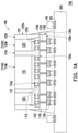
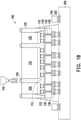
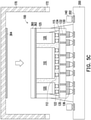
- FIG. 1A to FIG. 1C are cross-sectional views of a method of forming a package structure in accordance with a first embodiment.
- FIG. 2 is a top view of the package structure illustrated in FIG. 1C .
- a method of forming a package structure 10 includes following steps. First, an initial structure 10a illustrated in FIG. 1A is provided.
- the initial structure 10a includes a package 100 bonded on a circuit substrate 200 to form a chip-on-wafer-on-substrate (CoWoS) package, although it should be appreciated that embodiments may be applied to other 3DIC packages.
- CoWoS chip-on-wafer-on-substrate
- the package 100 may include a first die 110, a second die group having a plurality of second dies 120, an underfill layer 115, a first encapsulant 125, and an interposer 130.
- the first die 110 has a front-side 110a (i.e., an active surface) and a back-side 110b (i.e., a non-active surface) opposite to each other.
- Each second die 120 also has a front-side 120a (i.e., an active surface) and a back-side 120b (i.e., a non-active surface) opposite to each other.
- the first die 110 and the second dies 120 are flipped, so that the front-side 110a of the first die 110 and the front-sides 120a of the second dies 120 all face toward an upper surface 130a of the interposer 130.
- the first die 110 and the second dies 120 are bonded onto the upper surface 130a of the interposer 130 by a plurality of die connectors 112, 122, so as to form a chip-on-wafer (CoW) package, although it should be appreciated that embodiments may be applied to other 3DIC packages.
- CoW chip-on-wafer
- the first die 110 and the second dies 120 each has a single function (e.g., a logic device, memory die, etc.), or may have multiple functions (e.g., a SoC).
- the first die 110 is a processor and the second dies 120 are memory modules.
- the first die 110 is referred to as a die stack, which includes two bonded integrated circuit dies. The two integrated circuit dies are bonded such that the active surfaces are facing each other ("face-to-face") by hybrid bonding, fusion bonding, direct bonding, dielectric bonding, metal bonding, or the like.
- the first die 110 is a processor, such as a central processing unit (CPU), graphics processing unit (GPU), application-specific integrated circuit (ASIC), or the like.
- the first die 110 is a system-on-chip (SoC).
- the second dies 120 are memory devices, such as dynamic random access memory (DRAM) dies, static random access memory (SRAM) dies, hybrid memory cube (HMC) modules, high bandwidth memory (HBM) modules, or the like.
- DRAM dynamic random access memory
- SRAM static random access memory
- HMC hybrid memory cube
- HBM high bandwidth memory
- the second dies 120 is HBM modules.
- the die connectors 112, 122 is formed from a conductive material, such as solder, copper, aluminum, gold, nickel, silver, palladium, tin, the like, or a combination thereof.
- the die connectors 112, 122 are micro bumps including a solder sandwiched between two metal layers.
- a redistribution layer (RDL) structure 134 is optionally disposed between the die connectors 112, 122 and the upper surface 130a of the interposer 130 to electrically connect the die connectors 112, 122 and trough substrate vias (TSVs) 132 in the interposers 130.
- TSVs trough substrate vias
- the RDL structure 134 includes a plurality of polymer layers and a plurality of redistribution layers stacked alternately.
- the redistribution layers may be formed in the polymer layers to electrically connect the die connectors 112, 122 and the TSVs 132.
- the redistribution layers respectively include a plurality of vias and a plurality of traces connected to each other.
- the first die 110 and the second dies 120 may be electrically connected to the TSVs 132 in the interposer 130 by the die connectors 112, 122 and RDL structure 134.
- the underfill layer 115 is disposed between the first die 110 and the second dies 120 and laterally encapsulates the die connectors 112, 122.
- the underfill layer 115 is formed from any acceptable material, such as a polymer, epoxy, molding underfill, or the like.
- the underfill layer 115 may be formed by a capillary flow process after the first die 110 and the second dies 120 are attached or may be formed by a suitable deposition method before the first die 110 and the second dies 120 are attached.
- the first encapsulant 125 is disposed to laterally encapsulate the underfill layer 115 and the second dies 120.
- the first encapsulant 125 is formed from any acceptable material, such as a molding compound, epoxy, or the like.
- the first encapsulant 125 may be formed by compression molding, transfer molding, or the like.
- the first encapsulant 125 have fillers with average particle size greater than or equal to fillers of the underfill layer 115.
- the first encapsulant 125 may be formed over the interposer 130, such that the first die 110 and the second dies 120 are buried or covered.
- the first encapsulant 125 is then cured and planarized to expose the back-side 110b (top surface 110t) of the first die 110 and the back-sides 120b (top surfaces 120t) of the second dies 120 by a chemical mechanical polishing (CMP) process, a grinding process, or the like.
- CMP chemical mechanical polishing
- a top surface 125t of the first encapsulant 125, the top surface 110t of the first and second die 110, the top surfaces 120t of the second dies 120, and a top surface 115t of the underfill layer 115 are substantial level or coplanar.
- the package 100 is formed by performing a singulation process on a wafer including a plurality of first and second dies 110 and 120, the underfill layer 115, and the first encapsulant 125 thereon.
- the wafer is singulated into a plurality of interposers 130, with each of the packages 100 having one interposer 130.
- the singulation process includes a sawing process, a laser process, or a combination thereof.
- edges of the first encapsulant 125 and interposer 130 are coterminous, namely, a sidewall 125s of the first encapsulant 125 is substantially aligned with a sidewall 130s of the interposer 130.
- the CoW package 100 is bonded onto the circuit substrate 200 by a plurality of conductive connectors 136.
- the conductive connectors 136 are electrically and/or physically connected to the circuit substrate 200.
- the conductive connectors 136 may be BGA connectors, solder balls, metal pillars, controlled collapse chip connection (C4) bumps, micro bumps, electroless nickel-electroless palladium-immersion gold technique (ENEPIG) formed bumps, or the like.
- the conductive connectors 136 are formed by initially forming a layer of solder through such commonly used methods such as evaporation, electroplating, printing, solder transfer, ball placement, or the like. Once a layer of solder has been formed on the structure, a reflow may be performed in order to shape the material into the desired bump shapes.
- the circuit substrate 200 is made of a semiconductor material, such as silicon, germanium, diamond, or the like.
- compound materials such as silicon germanium, silicon carbide, gallium arsenic, indium arsenide, indium phosphide, silicon germanium carbide, gallium arsenic phosphide, gallium indium phosphide, combinations of these, and the like, may also be used.
- the circuit substrate 200 may be a SOI substrate.
- an SOI substrate includes a layer of a semiconductor material such as epitaxial silicon, germanium, silicon germanium, SOI, SGOI, or combinations thereof.
- the circuit substrate 200 is, in one alternative embodiment, based on an insulating core such as a fiberglass reinforced resin core.
- One example core material is fiberglass resin such as FR4.
- Alternatives for the core material include bismaleimide-triazine BT resin, or alternatively, other PCB materials or films. Build up films such as ABF or other laminates may be used for circuit substrate 200.
- the circuit substrate 200 may include active and passive devices (not shown), such as transistors, capacitors, resistors, combinations of these, and the like may be used to generate the structural and functional requirements of the design.
- the circuit substrate 200 may also include metallization layers and vias (not shown) and bond pads 202 over the metallization layers and vias.
- the metallization layers may be formed over the active and passive devices and are designed to connect the various devices to form functional circuitry.
- the metallization layers may be formed of alternating layers of dielectric (e.g., low-k dielectric material) and conductive material (e.g., copper) with vias interconnecting the layers of conductive material and may be formed through any suitable process (such as deposition, damascene, dual damascene, or the like).
- the circuit substrate 200 is substantially free of active and passive devices.
- the conductive connectors 136 are attached onto the bond pads 202, thereby bonding the interposer 130 to the circuit substrate 200.
- the conductive connectors 136 are electrically and/or physically connected the circuit substrate 200 to the package 100.
- a plurality of passive devices 140 e.g., surface mount devices (SMDs)
- SMDs surface mount devices
- the passive devices 140 are bonded to a same surface of the circuit substrate 200 as the conductive connectors 136.
- the conductive connectors 136 may have an epoxy flux (not shown) formed thereon before they are reflowed with at least some of the epoxy portion of the epoxy flux remaining after the package 100 is attached to the circuit substrate 200. This remaining epoxy portion may act as an underfill to reduce stress and protect the joints resulting from the reflowing the conductive connectors 136.
- a second encapsulant 135 is formed to laterally encapsulate the conductive connectors 136, the interposer 130, a lower sidewall of the first encapsulant 125.
- the second encapsulant 135 is formed from any suitable underfill material, such as a polymer, epoxy, molding underfill, or the like.
- the second encapsulant 135 may be formed by a capillary flow process after the package 100 is attached or may be formed by a suitable deposition method before the package 100 is attached.
- an adhesive pattern 150 is selectively dispensed on the underfill layer 115 between the first die 110 and the second dies 120 and on the first encapsulant 125 by a dispenser 152.
- the adhesive pattern 150 includes a polymer material, such as a liquid die attaching film (DAF), a polyimide (PI) based polymer, an epoxy based polymer, or the like.
- the adhesive pattern 150 is free of fillers.
- a thermal interface material (TIM) 160 is dispensed on the first die 110, the second dies 120, and the adhesive pattern 150.
- a lid 170 is then attached to the package 100 and circuit substrate 200 to form the package structure 10.
- the lid 170 covers and surrounds the package 100 and the passive devices 140.
- the lid 170 is formed from a material with high thermal conductivity (k), such as steel, stainless steel, copper, the like, or combinations thereof.
- the lid 170 is coated with another metal, such as gold, nickel, or the like.
- the lid 170 is a single contiguous material.
- the lid 170 includes multiple pieces that may be the same or different materials.
- the lid 170 is adhered to the package 100 by the TIM 160.
- the TIM 160 is sandwiched between the lid 170 and the first and second dies 110, 120, so as to thermally couple the lid 170 and the first and second dies 110, 120.
- the TIM 160 is formed to a thickness sufficiently large to bury the adhesive pattern 150. That is, as shown in FIG. 1C , the adhesive pattern 150 may be surrounded or wrapped by the TIM 160.
- the adhesive pattern 150 is formed to a height of about 0.5 ⁇ m to 100 ⁇ m, such as about 10 ⁇ m.
- the TIM 160 may be formed to a thickness of from about 5 ⁇ m to about 300 ⁇ m, such as about 60 ⁇ m.
- the thickness of the TIM is greater than the height or thickness of the adhesive pattern 150.
- the lid 170 is adhered to the circuit substrate 200 by an adhesive 172.
- the adhesive 172 is epoxy, glue, or the like.
- the adhesive 172 may be a thermally conductive material.
- the first die 110 and the second dies 120 may trap heat to become hot spots in the package structure 10. Therefore, the TIM 160 thermally couples the package 100 and lid 170 to dissipate the heat from the first and second dies 110, 120 to the lid 170.
- the adhesive pattern 150 may be disposed between the TIM 160 and the underfill layer 115 and/or the first encapsulant 125 to improve the adhesion between the TIM 160 and the underfill layer 115 and/or the first encapsulant 125, thereby decreasing the delamination issue and increasing the reliability. From the cross-sectional view of FIG. 1C , the adhesive pattern 150 may include a plurality of adhesive layers laterally spaced from each other.
- the adhesive layers are discretely distributed on the underfill layer 115 between the first and second dies 110 and 120 and on the first encapsulant 125.
- the adhesive pattern 150 separates the TIM 160 and the underfill layer 115 and/or the first encapsulant 125, so that the TIM 160 is not in (physical) contact with the underfill layer 115 and/or the first encapsulant 125.
- the TIM 160 and the adhesive pattern 150 have different materials.
- the TIM 160 may have a thermal conductivity (k) greater than a thermal conductivity of the adhesive pattern 150.
- k thermal conductivity
- an area of the TIM 160 contacting the top surfaces 110t, 120t of the first and second dies 110, 120 may be referred to as a thermal path for dissipating the heat from the first and second dies 110, 120.
- the TIM 160 is formed from a material with higher thermal conductivity (k), such as Ag, Cu, Sn, In, carbon nanotube (CNT), graphite, or the like.
- the adhesive pattern 150 may be formed from a material with lower thermal conductivity (k), such as a liquid die attaching film (DAF), a polyimide (PI) based polymer, an epoxy based polymer, or the like.
- k the thermal conductivity of the TIM 160 is from about 0.5 Wm -1 K -1 to about 200 Wm -1 K -1 , or from about 10 Wm -1 K -1 to about 50 Wm -1 K -1 , such as about 10 Wm -1 K 1 .
- the thermal conductivity (k) of the adhesive pattern 150 may be from about 0.5 Wm -1 K -1 to about 100 Wm -1 K -1 , or from about 0.5 Wm -1 K -1 to about 10 Wm -1 K -1 , such as about 2 Wm -1 K -1 .
- the TIM 160 is formed from another material, such as a polymer material, solder paste, indium solder paste, or the like.
- the thermal conductivity (k) of the TIM 160 is from about 0.5 Wm -1 K -1 to about 200 Wm -1 K -1 , or from about 10 Wm -1 K -1 to about 50 Wm -1 K -1 , such as about 10 Wm -1 K -1 .
- a first interface S1 is included between the adhesive pattern 150 and the TIM 160.
- the TIM 160 has a plurality of fillers, while the adhesive pattern 150 is free of fillers. Accordingly, the fillers in the TIM 160 may surround an upper surface of the adhesive pattern 150 to form the first interface S1.
- the adhesive pattern 150 and the underfill layer 115 may have different materials, thus a second interface S2 is included between the adhesive pattern 150 and the underfill layer 115.
- the underfill layer 115 has a plurality of fillers, while the adhesive pattern 150 is free of fillers. Accordingly, the fillers in the underfill layer 115 may surround a lower surface of the adhesive pattern 150 to form the second interface S2.
- the adhesive pattern 150 and the first encapsulant 125 have different materials, thus a third interface S3 is included between the adhesive pattern 150 and the first encapsulant 125.
- the first encapsulant 125 has a plurality of fillers, while the adhesive pattern 150 is free of fillers. Accordingly, the fillers in the first encapsulant 125 may surround a lower surface of the adhesive pattern 150 to form the third interface S3.
- the package structure 10 includes the first die 110 and the second dies 120 disposed side by side.
- the first die 110 is the SoC and the second dies 120 are HBM modules.
- an area of the first die 110 may be greater than an area of one of the second dies 120.
- the number of the second dies 120 may be greater than the number of the first die 110.
- the second dies 120 are disposed at both sides of the first die 110.
- the first die 110 and the second dies 120 may be electrically connected to each other by the RDL structure 134, the interposer 130, and the circuit substrate 200, as shown in FIG. 1C . As show in the top view of FIG.
- the adhesive pattern 150 has a plurality of openings 154 to expose the first and second dies 110 and 120.
- the adhesive pattern 150 is disposed on the underfill layer 115 and the first encapsulant 125, so as to surround a perimeter 110p of the first die 110 and perimeters 120p of the second dies 120 in the top view.
- the adhesive pattern 150 includes two adhesive layers respectively disposed on the underfill layer 115 between the first and second dies 110 and 120.
- the two adhesive layers may be disposed along both sides (e.g., right and left sides) of the first die 110.
- the adhesive pattern 150 includes a plurality of dot structures discretely distributed and surrounding the perimeter 110p of the first die 110 and perimeters 120p of the second dies 120 in the top view.
- a layout area of the adhesive pattern 150 is less than that of the whole package 100.
- a ratio of the layout area of the adhesive pattern 150 to the layout area of the package 100 is about 5% to about 99%.
- FIG. 3A and FIG. 3B are enlarged views of a portion 150p of the package structure 10 illustrated in FIG. 1C .
- an adhesive pattern 150a is formed and restricted on the underfill layer 115 without extending onto the top surfaces 110t, 120t of the first and second dies 110, 120.
- the adhesive pattern 150a may have a width W1 substantially equal to or less than a distance D1 between the first die 100 and the adjacent second die 120.
- the width W1 is about 10 ⁇ m to about 300 ⁇ m, such as 100 ⁇ m.
- the distance D1 may be about 10 ⁇ m to about 300 ⁇ m, such as 100 ⁇ m.
- the adhesive pattern 150a may have a flat bottom surface 150bt and a curved top surface 150t.
- the bottom surface 150bt of the adhesive pattern 150a is substantially aligned with the top surfaces 110t, 120t of the first and second dies 110, 120.
- the curved top surface 150t of the adhesive pattern 150a may be a convex surface that protrudes along a direction from the bottom surface 150bt to the top surface 150t.
- An included angle ⁇ 1 is between the top surface 150t and the bottom surface 150bt of the adhesive pattern 150a, wherein the included angle ⁇ may be an acute angle. In some embodiments, the included angle ⁇ 1 is about 5 degree to about 85 degree, such as 45 degree.
- a thickness T1 of the adhesive pattern 150a gradually decreases along a direction from center to edge. For example, the highest thickness T1 of the adhesive pattern 150a is about 0.5 ⁇ m to 100 ⁇ m, such as about 10 ⁇ m.
- an adhesive pattern 150b not only covers on the underfill layer 115, but also extends to cover a portion of the top surfaces 110t, 120t of the first and second dies 110, 120. In the case, the adhesive pattern 150b further covers and protects interfaces between the underfill layer 115 and the first and second dies 110, 120, thereby avoiding the defects.
- the adhesive pattern 150b may have a width W2 greater than the distance D1 between the first die 100 and the adjacent second die 120. In some embodiments, the width W2 is about 10 ⁇ m to about 300 ⁇ m, such as 140 ⁇ m. In the case, the adhesive pattern 150b may in contact with the portions of the top surfaces 110t, 120t of the first and second dies 110, 120.
- the adhesive pattern 150b may have an extending length L1 which is measured from an interface between the first die 110 and the underfill layer 115 to a right edge of the adhesive pattern 150b.
- the adhesive pattern 150b may have another extending length L2 which is measured from an interface between the second die 120 and the underfill layer 115 to a left edge of the adhesive pattern 150b.
- the extending length L1 is the same with the extending length L2.
- the extending length L1 is different from the extending length L2.
- the extending length L1 is about 3 ⁇ m to 60 ⁇ m, such as about 20 ⁇ m.
- the extending length L2 may be about 3 ⁇ m to 60 ⁇ m, such as about 20 ⁇ m.
- An included angle ⁇ 2 is between the top surface 150t' and the bottom surface 150bt' of the adhesive pattern 150b, wherein the included angle ⁇ 2 may be an acute angle. In some embodiments, the included angle ⁇ 2 is about 5 degree to about 85 degree, such as 45 degree. In one embodiment, the included angle ⁇ 2 is less than the included angle ⁇ 1. In other embodiments, the included angle ⁇ 2 is greater than or substantial equal to the included angle ⁇ 1.
- a thickness T2 of the adhesive pattern 150b also gradually decreases along the direction from center to edge. For example, the highest thickness T2 of the adhesive pattern 150b is about 0.5 ⁇ m to 100 ⁇ m, such as about 10 ⁇ m.
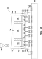
- FIG. 4A to FIG. 4C are cross-sectional views of a method of forming a package structure in accordance with a second embodiment.
- the CoWoS package 10a is provided.
- the structures, materials, and functions may be similar to what are shown in, and discussed referring to, FIG. 1A . The details are thus no repeated herein.
- a TIM 260 is dispensed on the first die 110, the second dies 120, the underfill layer 115, and the first encapsulant 125 by a dispenser 262.
- the TIM 260 includes a material with higher thermal conductivity (k), such as Ag, Cu, Sn, In, carbon nanotube (CNT), graphite, or the like.
- k thermal conductivity
- the TIM 260 has an edge thickness T3 greater than or substantially equal to a center thickness T4 of the TIM 260. The thicker edge thickness T3 may provide a better adhesion between the TIM 260 and the edge encapsulant 125, thereby decreasing the delamination issue and increasing the reliability for high-warpage area.
- the thinner center thickness T4 may achieve better thermal dissipation, especially from the first die 110 (e.g., SoC or GPU).
- the edge thickness T3 is about 5 ⁇ m to about 400 ⁇ m, such as about 200 ⁇ m; the center thickness T4 is about 3 ⁇ m to about 300 ⁇ m, such as about 100 ⁇ m; a ratio (T3/T4) of the edge thickness T3 to the center thickness T4 is about 1.1 to about 5, such as about 2.
- the specific range of the edge thickness T3 and/or the center thickness T4 of the TIM 260 may provide a better coverage than the thinner TIM and a better thermal dissipation than the thicker TIM.
- the TIM 260 may have a bad coverage without completely covering the underlying structure.
- the edge thickness T3 is greater than 400 ⁇ m and the center thickness T4 is greater than 300 ⁇ m, the TIM 260 may have a bad thermal dissipation.
- a lid 270 is then attached to the package 100 and circuit substrate 200 to form a package structure 20.
- the lid 270 covers and surrounds the package 100 and the passive devices 140.
- the lid 270 is adhered to the package 100 by the TIM 260 and adhered to the circuit substrate 200 by an adhesive 172. Since the TIM 260 has the thicker edge thickness T3 and the thinner center thickness T4, the TIM 260 has a concave top surface 260t.
- the concave top surface 260t may be recessed along a direction from the first die 110 to the interposer 130.
- the lid 270 may conformally covers the concave top surface 260t of the TIM 260 and has a concave top surface 270ct corresponding to the concave top surface 260t of the TIM 260. As shown in FIG. 4C , the lid 270 has a top surface 270t including a flat top surface 270ft and the concave top surface 270ct. The concave top surface 270ct is surrounded by the flat top surface 270ft. The flat top surface 270ft is higher than the concave top surface 270ct.
- the arrangement and material of the TIM 260 and the lid 270 are similar to the arrangement and material of the TIM 160 and the lid 170 and has been described in detail in the above embodiments. Thus, details thereof are omitted here.
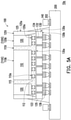
- FIG. 5A to FIG. 5D are cross-sectional views of a method of forming a package structure in accordance with a third embodiment.
- the CoWoS package 10a is provided.
- the structures, materials, and functions may be similar to what are shown in, and discussed referring to, FIG. 1A . The details are thus no repeated herein.
- a first metal layer 362 is formed on the package 100.
- the first metal layer 362 may be formed on the package 100 before or after the package 100 is singulated.
- the first metal layer 362 may be formed from a conductive material or metal, such as Ag, Au, Ti, NiV, Al, TiN, Cu, Sn, the like, or a combination thereof.
- the first metal layer 362 may be formed by depositing a seed layer over the interposer 130 (e.g., on the first encapsulant 125, the first and second dies 110, 120, and the underfill layer 115), and then electroplating the conductive material onto the seed layer.
- the first metal layer 362 may also be formed by sputtering the conductive material onto the package 100.
- the first metal layer 362 is a continuous structure that blanketly covers the first encapsulant 125, the first and second dies 110, 120, and the underfill layer 115. In some embodiments, the first metal layer 362 is electrically floating. That is, the first metal layer 362 may be electrically insulated from the active and/or passive devices of the first and second dies 110, 120 and other surrounding devices.
- a TIM 360 is then dispensed on the first metal layer 362.
- the material of the TIM 360 is similar to the material of the TIM 160 and has been described in detail in the above embodiments. Thus, details thereof are omitted here.
- the lid 170 coated with a second metal layer 364 is then attached to the package 100 and the circuit substrate 200 to form a package structure 30.
- the first metal layer 362, the second metal layer 364, and the TIM 360 sandwiched between the first and second metal layers 362, 364 constitutes a composite structure 365 to thermally couple the lid 170 and the first and second dies 110, 120.
- the second metal layer 364 may be formed from a conductive material or metal, such as Ag, Au, Ti, NiV, Al, TiN, Cu, Sn, the like, or a combination thereof.
- the second metal layer 364 may be formed by depositing a seed layer and then electroplating the conductive material onto the seed layer.
- the second metal layer 364 may also be formed by sputtering the conductive material onto an inner surface of the lid 170.
- the second metal layer 364 is a continuous structure that covers the TIM 360.
- the second metal layer 364 is electrically floating. That is, the second metal layer 364 may be electrically isolated from the active and/or passive devices of the first and second dies 110, 120 and other surrounding devices. Alternatively, the second metal layer 364 may be omitted and the TIM 360 is in contact with the lid 170.
- the first metal layer 362 and the second metal layer 364 have the same material or different materials.
- the first metal layer 362 has a thickness 362t substantially equal to a thickness 364t of the second metal layer 364.
- the thickness 362t of the first metal layer 362 may be about 0.1 ⁇ m to about 10 ⁇ m, such as about 1 ⁇ m.
- the thickness 364t of the second metal layer 364 may be about 0.1 ⁇ m to about 10 ⁇ m, such as about 1 ⁇ m.
- the specific range of the thickness 362t and/or the thickness 364t may provide a better coverage than the thinner metal layer and a better thermal dissipation than the thicker metal layer.
- the first metal layer 362 and/or the second metal layer 364 may have a bad coverage without completely covering the underlying structure.
- the thickness 362t and/or the thickness 364t is greater than 10 ⁇ m, the first metal layer 362 and/or the second metal layer 364 may have a bad thermal dissipation.
- the thickness 362t of the first metal layer 362 is less than or greater than the thickness 364t of the second metal layer 364.
- the TIM 360 has a thickness 360t greater than or substantially equal to the thickness 362t of the first metal layer 362 and/or the thickness 364t of the second metal layer 364.
- the thickness 360t of the TIM 360 may be about 3 ⁇ m to about 300 ⁇ m, such as about 60 ⁇ m.
- the first metal layer 362 may improve an adhesion between the TIM 360 and the package 100 (especially the underfill layer 115 and the first encapsulant 125), thereby decreasing the delamination issue and increasing the reliability.
- the first metal layer 362 may be referred to as an adhesive film, layer, or pattern.
- the second metal layer 364 may improve an adhesion between the TIM 360 and the lid 170, thereby decreasing the delamination issue and increasing the reliability.
- the second metal layer 364 may also be referred to as an adhesive film, layer, or pattern.
- the composite structure 365 including the TIM 360 sandwiched between the first metal layer 362 and the second metal layer 364 may have a high thermal conductivity and may conform to the shape of the package 100, including conforming to any warpage that may have been introduced in the package 100. As such, the overall thermal resistance of the package structure 30 may be reduced.
- FIG. 6 illustrates a package structure 40 having an adhesive pattern 450 and the TIM 260.
- the adhesive pattern 450 is dispensed on the underfill layer 115.
- the TIM 260 with different thickness is then dispensed on the adhesive pattern 450, the first encapsulant 125, and the first and second dies 110 and 120, so that the adhesive pattern 450 is surrounded by the TIM 260.
- the material of the adhesive pattern 450 is similar to the material of the adhesive pattern 150 and has been described in detail in the above embodiments. Thus, details thereof are omitted here.
- the package structure 40 may have advantages combined from the package structures 10 and 20. That is, the adhesive pattern 450 may improve the adhesion between the TIM 260 and the underfill layer 115.
- the thicker edge thickness T3 may improve the adhesion between the TIM 260 and the edge encapsulant 125, thereby decreasing the delamination issue and increasing the reliability for high-warpage area.
- the thinner center thickness T4 may achieve better thermal dissipation, especially from the first die 110 (e.g., SoC or GPU).
- the adhesive pattern 450 is formed and restricted on the underfill layer 115. In some other embodiments, the adhesive pattern 450 extends to cover portions of the first and second dies 110, 120. In some embodiments, a layout area of the adhesive pattern 450 is less than that of the adhesive pattern 150 illustrated in FIG. 2 .
- a ratio of the layout area of the adhesive pattern 450 to the layout area of the package 100 is about 5% to about 99%.
- the adhesive pattern 450 may be optionally formed on the first encapsulant 125 to separate the first encapsulant 125 from the TIM 260.
- a package structure includes a first die, a second die group, an interposer, an underfill layer, a thermal interface material (TIM), and an adhesive pattern.
- the first die and the second die group are disposed side by side on the interposer.
- the underfill layer is disposed between the first die and the second die group.
- the TIM is disposed on the first die, the second die group, and the underfill layer.
- the adhesive pattern is disposed between the underfill layer and the TIM to separate the underfill layer from the TIM.
- a package structure includes a first die, a second die, an interposer, an underfill layer, a thermal interface material (TIM), and a first metal layer.
- the first die and the second die are disposed side by side on the interposer.
- the TIM is disposed on the first die, the second die, and the underfill layer.
- the TIM has an edge thickness greater than a center thickness of the TIM.
- a method of forming a package structure includes: bonding a first die and a second die onto an interposer; dispensing an underfill layer between the first die and the second die; forming a first encapsulant to laterally encapsulate the first die, the second die, and the underfill layer; forming an adhesive pattern on the underfill layer between the first die and the second die and on the first encapsulant; and dispensing a thermal interface material (TIM) on the adhesive pattern.
- TIM thermal interface material
Landscapes
- Structures Or Materials For Encapsulating Or Coating Semiconductor Devices Or Solid State Devices (AREA)
- Engineering & Computer Science (AREA)
- Manufacturing & Machinery (AREA)
- Physics & Mathematics (AREA)
- Geometry (AREA)
- Die Bonding (AREA)
- Cooling Or The Like Of Semiconductors Or Solid State Devices (AREA)
Applications Claiming Priority (1)
| Application Number | Priority Date | Filing Date | Title |
|---|---|---|---|
| US16/941,509 US11239136B1 (en) | 2020-07-28 | 2020-07-28 | Adhesive and thermal interface material on a plurality of dies covered by a lid |
Publications (2)
| Publication Number | Publication Date |
|---|---|
| EP3958304A2 true EP3958304A2 (de) | 2022-02-23 |
| EP3958304A3 EP3958304A3 (de) | 2022-09-14 |
Family
ID=77367231
Family Applications (1)
| Application Number | Title | Priority Date | Filing Date |
|---|---|---|---|
| EP21188007.5A Withdrawn EP3958304A3 (de) | 2020-07-28 | 2021-07-27 | Gehäusestruktur und verfahren zur formung davon |
Country Status (5)
| Country | Link |
|---|---|
| US (4) | US11239136B1 (de) |
| EP (1) | EP3958304A3 (de) |
| JP (1) | JP2022025048A (de) |
| CN (1) | CN113451285B (de) |
| TW (1) | TWI753587B (de) |
Families Citing this family (13)
| Publication number | Priority date | Publication date | Assignee | Title |
|---|---|---|---|---|
| US11239136B1 (en) * | 2020-07-28 | 2022-02-01 | Taiwan Semiconductor Manufacturing Company, Ltd. | Adhesive and thermal interface material on a plurality of dies covered by a lid |
| US11682602B2 (en) | 2021-02-04 | 2023-06-20 | Taiwan Semiconductor Manufacturing Co., Ltd. | Semiconductor device and method of manufacture |
| US12525497B2 (en) * | 2021-12-21 | 2026-01-13 | Intel Corporation | Microelectronic assemblies with adaptive multi-layer encapsulation materials |
| US20230317535A1 (en) * | 2022-03-31 | 2023-10-05 | Taiwan Semiconductor Manufacturing Company, Ltd. | Package structure and method for fabricating the same |
| US20230378017A1 (en) * | 2022-05-17 | 2023-11-23 | Taiwan Semiconductor Manufacturing Co., Ltd. | Integrated circuit packages and methods of forming the same |
| US12593711B2 (en) * | 2022-06-30 | 2026-03-31 | Taiwan Semiconductor Manufacturing Company, Ltd. | Bonding structure with stress buffer zone and method of forming same |
| US20240038623A1 (en) * | 2022-07-28 | 2024-02-01 | Taiwan Semiconductor Manufacturing Co., Ltd. | Integrated Circuit Packages and Methods of Forming the Same |
| US12424558B2 (en) * | 2022-08-12 | 2025-09-23 | Taiwan Semiconductor Manufacturing Company, Ltd. | Bridge die having different surface orientation than IC dies interconnected by the bridge die |
| US12482735B2 (en) * | 2022-08-30 | 2025-11-25 | Taiwan Semiconductor Manufacturing Company Limited | Semiconductor package including a surface with a plurality of roughness values and methods of forming the same |
| US20240071857A1 (en) * | 2022-08-31 | 2024-02-29 | Taiwan Semiconductor Manufacturing Company, Ltd. | Semiconductor device |
| WO2024132174A1 (en) | 2022-12-22 | 2024-06-27 | Bitzer Kühlmaschinenbau Gmbh | Machine for expanding or compressing compressible media |
| CN115985863A (zh) * | 2023-03-06 | 2023-04-18 | 日月新半导体(昆山)有限公司 | 集成电路封装产品 |
| US20250112110A1 (en) * | 2023-10-02 | 2025-04-03 | Stmicroelectronics International N.V. | Thermally enhanced flip chip ball grid array package with improved heat dissipation |
Family Cites Families (41)
| Publication number | Priority date | Publication date | Assignee | Title |
|---|---|---|---|---|
| US7168484B2 (en) * | 2003-06-30 | 2007-01-30 | Intel Corporation | Thermal interface apparatus, systems, and methods |
| US7023089B1 (en) * | 2004-03-31 | 2006-04-04 | Intel Corporation | Low temperature packaging apparatus and method |
| US7183641B2 (en) * | 2005-03-30 | 2007-02-27 | Intel Corporation | Integrated heat spreader with intermetallic layer and method for making |
| US7651938B2 (en) * | 2006-06-07 | 2010-01-26 | Advanced Micro Devices, Inc. | Void reduction in indium thermal interface material |
| US7678615B2 (en) * | 2007-08-29 | 2010-03-16 | Advanced Micro Devices, Inc. | Semiconductor device with gel-type thermal interface material |
| US20090057884A1 (en) * | 2007-08-29 | 2009-03-05 | Seah Sun Too | Multi-Chip Package |
| US7956456B2 (en) * | 2008-02-27 | 2011-06-07 | Texas Instruments Incorporated | Thermal interface material design for enhanced thermal performance and improved package structural integrity |
| US7961469B2 (en) * | 2009-03-31 | 2011-06-14 | Apple Inc. | Method and apparatus for distributing a thermal interface material |
| US8304291B2 (en) * | 2009-06-29 | 2012-11-06 | Advanced Micro Devices, Inc. | Semiconductor chip thermal interface structures |
| US8039304B2 (en) * | 2009-08-12 | 2011-10-18 | Stats Chippac, Ltd. | Semiconductor device and method of dual-molding die formed on opposite sides of build-up interconnect structures |
| US8299633B2 (en) * | 2009-12-21 | 2012-10-30 | Advanced Micro Devices, Inc. | Semiconductor chip device with solder diffusion protection |
| US8797057B2 (en) | 2011-02-11 | 2014-08-05 | Taiwan Semiconductor Manufacturing Company, Ltd. | Testing of semiconductor chips with microbumps |
| JP5799565B2 (ja) * | 2011-04-22 | 2015-10-28 | 株式会社ソシオネクスト | 半導体装置及びその製造方法 |
| US9385006B2 (en) * | 2012-06-21 | 2016-07-05 | STATS ChipPAC Pte. Ltd. | Semiconductor device and method of forming an embedded SOP fan-out package |
| US9443783B2 (en) | 2012-06-27 | 2016-09-13 | Taiwan Semiconductor Manufacturing Company, Ltd. | 3DIC stacking device and method of manufacture |
| US9299649B2 (en) | 2013-02-08 | 2016-03-29 | Taiwan Semiconductor Manufacturing Company, Ltd. | 3D packages and methods for forming the same |
| US9287194B2 (en) * | 2013-03-06 | 2016-03-15 | Taiwan Semiconductor Manufacturing Company, Ltd. | Packaging devices and methods for semiconductor devices |
| US8993380B2 (en) | 2013-03-08 | 2015-03-31 | Taiwan Semiconductor Manufacturing Company, Ltd. | Structure and method for 3D IC package |
| US9281254B2 (en) | 2014-02-13 | 2016-03-08 | Taiwan Semiconductor Manufacturing Company, Ltd. | Methods of forming integrated circuit package |
| US9425126B2 (en) | 2014-05-29 | 2016-08-23 | Taiwan Semiconductor Manufacturing Company, Ltd. | Dummy structure for chip-on-wafer-on-substrate |
| US9496189B2 (en) | 2014-06-13 | 2016-11-15 | Taiwan Semiconductor Manufacturing Company, Ltd. | Stacked semiconductor devices and methods of forming same |
| US9461018B1 (en) | 2015-04-17 | 2016-10-04 | Taiwan Semiconductor Manufacturing Company, Ltd. | Fan-out PoP structure with inconsecutive polymer layer |
| US9666502B2 (en) | 2015-04-17 | 2017-05-30 | Taiwan Semiconductor Manufacturing Company, Ltd. | Discrete polymer in fan-out packages |
| US9735131B2 (en) | 2015-11-10 | 2017-08-15 | Taiwan Semiconductor Manufacturing Company, Ltd. | Multi-stack package-on-package structures |
| WO2017123188A1 (en) * | 2016-01-11 | 2017-07-20 | Intel Corporation | Multiple-chip package with multiple thermal interface materials |
| US9831148B2 (en) | 2016-03-11 | 2017-11-28 | Taiwan Semiconductor Manufacturing Company, Ltd. | Integrated fan-out package including voltage regulators and methods forming same |
| US10770405B2 (en) * | 2017-05-31 | 2020-09-08 | Taiwan Semiconductor Manufacturing Company, Ltd. | Thermal interface material having different thicknesses in packages |
| US10529645B2 (en) * | 2017-06-08 | 2020-01-07 | Xilinx, Inc. | Methods and apparatus for thermal interface material (TIM) bond line thickness (BLT) reduction and TIM adhesion enhancement for efficient thermal management |
| US10461014B2 (en) | 2017-08-31 | 2019-10-29 | Taiwan Semiconductor Manufacturing Company, Ltd. | Heat spreading device and method |
| US10607857B2 (en) * | 2017-12-06 | 2020-03-31 | Indium Corporation | Semiconductor device assembly including a thermal interface bond between a semiconductor die and a passive heat exchanger |
| CN108717939B (zh) * | 2018-06-01 | 2020-06-12 | 京东方科技集团股份有限公司 | 静电释放保护电路、阵列基板和显示装置 |
| US10756058B2 (en) * | 2018-08-29 | 2020-08-25 | Taiwan Semiconductor Manufacturing Co., Ltd. | Semiconductor package and manufacturing method thereof |
| US11062971B2 (en) * | 2019-01-08 | 2021-07-13 | Taiwan Semiconductor Manufacturing Company, Ltd. | Package structure and method and equipment for forming the same |
| US11289401B2 (en) * | 2019-05-15 | 2022-03-29 | Powertech Technology Inc. | Semiconductor package |
| US11682605B2 (en) * | 2019-05-28 | 2023-06-20 | Intel Corporation | Integrated circuit packages with asymmetric adhesion material regions |
| US11935799B2 (en) * | 2019-06-25 | 2024-03-19 | Intel Corporation | Integrated circuit package lids with polymer features |
| US11705417B2 (en) * | 2019-10-08 | 2023-07-18 | Intel Corporation | Backside metallization (BSM) on stacked die packages and external silicon at wafer level, singulated die level, or stacked dies level |
| CN113035788B (zh) * | 2019-12-25 | 2025-03-14 | 台湾积体电路制造股份有限公司 | 封装结构及其制作方法 |
| US11239134B2 (en) * | 2020-01-17 | 2022-02-01 | Taiwan Semiconductor Manufacturing Company, Ltd. | Package structure and method of fabricating the same |
| US11239136B1 (en) * | 2020-07-28 | 2022-02-01 | Taiwan Semiconductor Manufacturing Company, Ltd. | Adhesive and thermal interface material on a plurality of dies covered by a lid |
| US11469197B2 (en) * | 2020-08-26 | 2022-10-11 | Taiwan Semiconductor Manufacturing Co., Ltd. | Integrated circuit package and method |
-
2020
- 2020-07-28 US US16/941,509 patent/US11239136B1/en active Active
- 2020-09-25 TW TW109133245A patent/TWI753587B/zh active
- 2020-09-29 CN CN202011048755.0A patent/CN113451285B/zh active Active
-
2021
- 2021-07-27 EP EP21188007.5A patent/EP3958304A3/de not_active Withdrawn
- 2021-07-27 JP JP2021122516A patent/JP2022025048A/ja active Pending
-
2022
- 2022-01-21 US US17/580,662 patent/US11626344B2/en active Active
-
2023
- 2023-03-10 US US18/181,552 patent/US11894287B2/en active Active
-
2024
- 2024-02-05 US US18/432,061 patent/US12300574B2/en active Active
Also Published As
| Publication number | Publication date |
|---|---|
| TWI753587B (zh) | 2022-01-21 |
| US20220139802A1 (en) | 2022-05-05 |
| CN113451285A (zh) | 2021-09-28 |
| US11239136B1 (en) | 2022-02-01 |
| EP3958304A3 (de) | 2022-09-14 |
| JP2022025048A (ja) | 2022-02-09 |
| US20240234244A1 (en) | 2024-07-11 |
| TW202205571A (zh) | 2022-02-01 |
| US11626344B2 (en) | 2023-04-11 |
| US20230230898A1 (en) | 2023-07-20 |
| CN113451285B (zh) | 2025-04-29 |
| US12300574B2 (en) | 2025-05-13 |
| US20220037229A1 (en) | 2022-02-03 |
| US11894287B2 (en) | 2024-02-06 |
Similar Documents
| Publication | Publication Date | Title |
|---|---|---|
| US11894287B2 (en) | Adhesive and thermal interface material on a plurality of dies covered by a lid | |
| US12080615B2 (en) | Method of manufacturing an integrated fan-out package having fan-out redistribution layer (RDL) to accommodate electrical connectors | |
| US11984372B2 (en) | Integrated circuit package and method | |
| US20230114652A1 (en) | Integrated Fan-Out Package and the Methods of Manufacturing | |
| US12021008B2 (en) | Thermal interface materials, 3D semiconductor packages and methods of manufacture | |
| US11817410B2 (en) | Integrated circuit package and method | |
| US11637084B2 (en) | Semiconductor package having a through intervia through the molding compound and fan-out redistribution layers disposed over the respective die of the stacked fan-out system-in-package | |
| TWI765601B (zh) | 半導體裝置及製造方法 | |
| US20250309029A1 (en) | Integrated circuit packages and methods of forming the same | |
| US20250174576A1 (en) | Semiconductor package and fabrication method thereof | |
| US20240379535A1 (en) | Semiconductor packages and methods of forming same | |
| US20250329666A1 (en) | Stress buffer in integrated circuit package and method | |
| US20250105086A1 (en) | Integrated Circuit Packages and Methods of Forming the Same | |
| TW202310085A (zh) | 封裝結構及其形成方法 | |
| US20240071857A1 (en) | Semiconductor device | |
| US20250118608A1 (en) | Integrated circuit packages and methods of forming the same | |
| KR20210133125A (ko) | 반도체 디바이스 및 방법 |
Legal Events
| Date | Code | Title | Description |
|---|---|---|---|
| PUAI | Public reference made under article 153(3) epc to a published international application that has entered the european phase |
Free format text: ORIGINAL CODE: 0009012 |
|
| STAA | Information on the status of an ep patent application or granted ep patent |
Free format text: STATUS: THE APPLICATION HAS BEEN PUBLISHED |
|
| AK | Designated contracting states |
Kind code of ref document: A2 Designated state(s): AL AT BE BG CH CY CZ DE DK EE ES FI FR GB GR HR HU IE IS IT LI LT LU LV MC MK MT NL NO PL PT RO RS SE SI SK SM TR |
|
| RIC1 | Information provided on ipc code assigned before grant |
Ipc: H01L 23/42 20060101ALN20220509BHEP Ipc: H01L 23/498 20060101ALN20220509BHEP Ipc: H01L 23/50 20060101ALN20220509BHEP Ipc: H01L 23/538 20060101ALN20220509BHEP Ipc: H01L 25/18 20060101ALI20220509BHEP Ipc: H01L 23/04 20060101ALI20220509BHEP Ipc: H01L 21/56 20060101ALI20220509BHEP Ipc: H01L 25/065 20060101ALI20220509BHEP Ipc: H01L 23/373 20060101ALI20220509BHEP Ipc: H01L 23/367 20060101ALI20220509BHEP Ipc: H01L 23/31 20060101AFI20220509BHEP |
|
| PUAL | Search report despatched |
Free format text: ORIGINAL CODE: 0009013 |
|
| AK | Designated contracting states |
Kind code of ref document: A3 Designated state(s): AL AT BE BG CH CY CZ DE DK EE ES FI FR GB GR HR HU IE IS IT LI LT LU LV MC MK MT NL NO PL PT RO RS SE SI SK SM TR |
|
| RIC1 | Information provided on ipc code assigned before grant |
Ipc: H01L 23/42 20060101ALN20220811BHEP Ipc: H01L 23/498 20060101ALN20220811BHEP Ipc: H01L 23/50 20060101ALN20220811BHEP Ipc: H01L 23/538 20060101ALN20220811BHEP Ipc: H01L 25/18 20060101ALI20220811BHEP Ipc: H01L 23/04 20060101ALI20220811BHEP Ipc: H01L 21/56 20060101ALI20220811BHEP Ipc: H01L 25/065 20060101ALI20220811BHEP Ipc: H01L 23/373 20060101ALI20220811BHEP Ipc: H01L 23/367 20060101ALI20220811BHEP Ipc: H01L 23/31 20060101AFI20220811BHEP |
|
| STAA | Information on the status of an ep patent application or granted ep patent |
Free format text: STATUS: THE APPLICATION IS DEEMED TO BE WITHDRAWN |
|
| 18D | Application deemed to be withdrawn |
Effective date: 20230315 |