EP3955507A1 - Phase synchronization device - Google Patents
Phase synchronization device Download PDFInfo
- Publication number
- EP3955507A1 EP3955507A1 EP19928647.7A EP19928647A EP3955507A1 EP 3955507 A1 EP3955507 A1 EP 3955507A1 EP 19928647 A EP19928647 A EP 19928647A EP 3955507 A1 EP3955507 A1 EP 3955507A1
- Authority
- EP
- European Patent Office
- Prior art keywords
- phase
- signal
- output
- interpolator
- shifter
- Prior art date
- Legal status (The legal status is an assumption and is not a legal conclusion. Google has not performed a legal analysis and makes no representation as to the accuracy of the status listed.)
- Granted
Links
Images





Classifications
-
- H—ELECTRICITY
- H03—ELECTRONIC CIRCUITRY
- H03L—AUTOMATIC CONTROL, STARTING, SYNCHRONISATION OR STABILISATION OF GENERATORS OF ELECTRONIC OSCILLATIONS OR PULSES
- H03L7/00—Automatic control of frequency or phase; Synchronisation
- H03L7/06—Automatic control of frequency or phase; Synchronisation using a reference signal applied to a frequency- or phase-locked loop
- H03L7/08—Details of the phase-locked loop
- H03L7/081—Details of the phase-locked loop provided with an additional controlled phase shifter
- H03L7/0812—Details of the phase-locked loop provided with an additional controlled phase shifter and where no voltage or current controlled oscillator is used
- H03L7/0814—Details of the phase-locked loop provided with an additional controlled phase shifter and where no voltage or current controlled oscillator is used the phase shifting device being digitally controlled
-
- H—ELECTRICITY
- H03—ELECTRONIC CIRCUITRY
- H03L—AUTOMATIC CONTROL, STARTING, SYNCHRONISATION OR STABILISATION OF GENERATORS OF ELECTRONIC OSCILLATIONS OR PULSES
- H03L7/00—Automatic control of frequency or phase; Synchronisation
- H03L7/06—Automatic control of frequency or phase; Synchronisation using a reference signal applied to a frequency- or phase-locked loop
- H03L7/07—Automatic control of frequency or phase; Synchronisation using a reference signal applied to a frequency- or phase-locked loop using several loops, e.g. for redundant clock signal generation
-
- G—PHYSICS
- G06—COMPUTING OR CALCULATING; COUNTING
- G06F—ELECTRIC DIGITAL DATA PROCESSING
- G06F7/00—Methods or arrangements for processing data by operating upon the order or content of the data handled
- G06F7/38—Methods or arrangements for performing computations using exclusively denominational number representation, e.g. using binary, ternary, decimal representation
- G06F7/48—Methods or arrangements for performing computations using exclusively denominational number representation, e.g. using binary, ternary, decimal representation using non-contact-making devices, e.g. tube, solid state device; using unspecified devices
- G06F7/50—Adding; Subtracting
- G06F7/501—Half or full adders, i.e. basic adder cells for one denomination
-
- H—ELECTRICITY
- H03—ELECTRONIC CIRCUITRY
- H03L—AUTOMATIC CONTROL, STARTING, SYNCHRONISATION OR STABILISATION OF GENERATORS OF ELECTRONIC OSCILLATIONS OR PULSES
- H03L7/00—Automatic control of frequency or phase; Synchronisation
- H03L7/06—Automatic control of frequency or phase; Synchronisation using a reference signal applied to a frequency- or phase-locked loop
- H03L7/08—Details of the phase-locked loop
- H03L7/085—Details of the phase-locked loop concerning mainly the frequency- or phase-detection arrangement including the filtering or amplification of its output signal
- H03L7/093—Details of the phase-locked loop concerning mainly the frequency- or phase-detection arrangement including the filtering or amplification of its output signal using special filtering or amplification characteristics in the loop
-
- H—ELECTRICITY
- H03—ELECTRONIC CIRCUITRY
- H03L—AUTOMATIC CONTROL, STARTING, SYNCHRONISATION OR STABILISATION OF GENERATORS OF ELECTRONIC OSCILLATIONS OR PULSES
- H03L7/00—Automatic control of frequency or phase; Synchronisation
- H03L7/06—Automatic control of frequency or phase; Synchronisation using a reference signal applied to a frequency- or phase-locked loop
- H03L7/08—Details of the phase-locked loop
- H03L7/085—Details of the phase-locked loop concerning mainly the frequency- or phase-detection arrangement including the filtering or amplification of its output signal
- H03L7/097—Details of the phase-locked loop concerning mainly the frequency- or phase-detection arrangement including the filtering or amplification of its output signal using a comparator for comparing the voltages obtained from two frequency to voltage converters
-
- H—ELECTRICITY
- H03—ELECTRONIC CIRCUITRY
- H03L—AUTOMATIC CONTROL, STARTING, SYNCHRONISATION OR STABILISATION OF GENERATORS OF ELECTRONIC OSCILLATIONS OR PULSES
- H03L7/00—Automatic control of frequency or phase; Synchronisation
- H03L7/06—Automatic control of frequency or phase; Synchronisation using a reference signal applied to a frequency- or phase-locked loop
- H03L7/08—Details of the phase-locked loop
- H03L7/099—Details of the phase-locked loop concerning mainly the controlled oscillator of the loop
- H03L7/0995—Details of the phase-locked loop concerning mainly the controlled oscillator of the loop the oscillator comprising a ring oscillator
- H03L7/0998—Details of the phase-locked loop concerning mainly the controlled oscillator of the loop the oscillator comprising a ring oscillator using phase interpolation
-
- H—ELECTRICITY
- H03—ELECTRONIC CIRCUITRY
- H03L—AUTOMATIC CONTROL, STARTING, SYNCHRONISATION OR STABILISATION OF GENERATORS OF ELECTRONIC OSCILLATIONS OR PULSES
- H03L7/00—Automatic control of frequency or phase; Synchronisation
- H03L7/06—Automatic control of frequency or phase; Synchronisation using a reference signal applied to a frequency- or phase-locked loop
- H03L7/16—Indirect frequency synthesis, i.e. generating a desired one of a number of predetermined frequencies using a frequency- or phase-locked loop
- H03L7/22—Indirect frequency synthesis, i.e. generating a desired one of a number of predetermined frequencies using a frequency- or phase-locked loop using more than one loop
-
- H—ELECTRICITY
- H01—ELECTRIC ELEMENTS
- H01Q—ANTENNAS, i.e. RADIO AERIALS
- H01Q3/00—Arrangements for changing or varying the orientation or the shape of the directional pattern of the waves radiated from an antenna or antenna system
- H01Q3/26—Arrangements for changing or varying the orientation or the shape of the directional pattern of the waves radiated from an antenna or antenna system varying the relative phase or relative amplitude of energisation between two or more active radiating elements; varying the distribution of energy across a radiating aperture
- H01Q3/30—Arrangements for changing or varying the orientation or the shape of the directional pattern of the waves radiated from an antenna or antenna system varying the relative phase or relative amplitude of energisation between two or more active radiating elements; varying the distribution of energy across a radiating aperture varying the relative phase between the radiating elements of an array
- H01Q3/34—Arrangements for changing or varying the orientation or the shape of the directional pattern of the waves radiated from an antenna or antenna system varying the relative phase or relative amplitude of energisation between two or more active radiating elements; varying the distribution of energy across a radiating aperture varying the relative phase between the radiating elements of an array by electrical means
Definitions
- the present invention relates to a phase synchronization device including a plurality of cascaded elements.
- a phase synchronization device including a plurality of elements with output phases equal to each other may be used for an active phased array antenna (APAA) or a very large scale integration (VLSI).
- APAA active phased array antenna
- VLSI very large scale integration
- Each of the elements detects a phase difference between the phase of a reference signal and the phase of a signal that is referred to, returns the phases so that the detected phase difference is 0, and can thus output a signal with a stable frequency.
- phase rotation amount A a phase rotation amount due to the difference between the path lengths
- phase rotation amounts B the phase rotation amounts caused in the elements vary depending on the gains depending on the elements. As a result, the output phases of the elements may be deviated from each other.
- a phase synchronization device described in Non-patent Literature 1 detects and returns a phase difference between elements caused by the phase rotation amounts A and B to correct the phase difference between the output phases of the elements.
- Non-patent Literature 1 Toshihiro Shimura, Takenori Ohshima, Hiroshi Ashida, Shohei Ishikawa, Shunsuke Fujio, Atsushi Hyundai, Zhengyi Li, Kenichi Nishikawa, Chikara Kojima, Kazuyuki Ozaki, Masahiko Shimizu and Yoji Ohashi, "Millimeter-Wave TX Phased Array with Phase Adjusting Function between Transmitters for Hybrid Beamforming with Interleaved Subarrays", Proceedings of the 46th European Microwave Conference, October 2016, pp. 1572-1575 .
- phase rotation amounts C phase rotation amounts due to wire delays through the lines connecting the elements are caused in addition to the phase rotation amounts A and B, and these amounts cannot be distinguished from each other.
- phase rotation amounts C phase rotation amounts due to wire delays through the lines connecting the elements are caused in addition to the phase rotation amounts A and B, and these amounts cannot be distinguished from each other.
- phase rotation amounts C have changed in addition to the phase rotation amounts A and the phase rotation amounts B by changes in environmental conditions, for example, there is a problem in that the phase differences between the output phases of the elements cannot be accurately corrected, and the output phases of the elements are not equal to each other.
- the present invention has been made to solve the aforementioned problem, and an object thereof is to provide a phase synchronization device capable of making output phases of a plurality of elements equal to each other.
- a phase synchronization device is a phase synchronization device including a plurality of cascaded elements, the elements each including a phase interpolator, a phase shifter, a phase comparator, and a control circuit, wherein the phase interpolator receives input of a first signal based on a reference signal input via a line and a second signal output from the phase shifter included in an element of a previous stage, and generates and outputs a third signal having a phase intermediate between the first signal and the second signal, the phase shifter outputs, as the second signal, the third signal with a phase shifted by a first phase shift amount to the phase interpolator included in an element of a subsequent stage, the phase comparator detects a phase difference between the third signal and a fourth signal obtained by shifting a phase of the first signal output from the element of the subsequent stage by the first phase shift amount, and the control circuit controls the first phase shift amount for the phase shifter on a basis of the phase difference detected by the phase comparator.
- a third signal having a phase intermediate between a first signal based on a reference signal and a second signal phase shifted by an element of a previous stage is generated, a signal obtained by shifting the phase of the third signal by a first phase shift amount is output as a second signal to an element of a subsequent stage, a phase difference between the third signal and a fourth signal obtained by shifting the phase of a first signal output from the element of the subsequent stage by the first phase shift amount is detected, and the first phase shift amount is controlled on the basis of the detected phase difference.
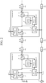
- FIG. 1 is a block diagram illustrating a configuration of a phase synchronization device according to a first embodiment.
- the phase synchronization device illustrated in FIG. 1 is a device including a plurality of elements, which are cascaded by a line 1a for transmitting and receiving signals to/from each other and a line 1b through which a reference signal from a reference signal source 1 propagates.
- the PLL circuit 2 generates and outputs a first signal based on the reference signal input via the line 1b. For example, the PLL circuit 2 performs frequency multiplication of the reference signal to output a signal with a known frequency (a signal with a radio frequency (RF)) higher than the frequency of the reference signal.
- RF radio frequency
- a phase rotation amount ⁇ 1 + ⁇ 2 + ⁇ 3 +...+ ⁇ n-1 due to a wire delay is added to the phase of the reference signal input through the line 1b.
- the phase ⁇ n of the first signal includes the phase rotation amount generated in the element #n and the phase rotation amount of the reference signal due to the wire delay.
- the first signal with the phase ⁇ n generated by the PLL circuit 2 is output to the directional coupler 3 and the phase interpolator 4.
- the directional coupler 3 included in the element #n outputs the first signal to a previous ((n-1)-th) element #n-1 via the line 1a. While the first signal propagates through the line 1a from the element #n to the element #n-1, a phase rotation amount ⁇ n-1 due to a wire delay is added to the phase ⁇ n of the first signal.
- the directional coupler 3 receives input of a second signal with a phase shifted by a variable phase shifter 5 included in the previous element #n-1 via the same line 1a, and outputs the second signal to the phase interpolator 4. While the second signal propagates through the line 1a from the element #n-1 to the element #n, a phase rotation amount ⁇ n-1 due to a wire delay is added to the phase of the second signal.
- the phase interpolator 4 included in the element #n receives input of the first signal with the phase ⁇ n output from the PLL circuit 2 and the second signal with the phase shifted in the element #n-1, and generates a third signal having a phase ⁇ out_n that is intermediate between these signals.
- the third signal is output as an output signal from the element #n.
- the third signal generated by the phase interpolator 4 is also output to the variable phase shifter 5 and the phase comparator 8.
- the variable phase shifter 5 is a first phase shifter that shifts the phase of an input signal by a phase shift amount ⁇ n , which is a first phase shift amount, controlled by the control circuit 9.
- the variable phase shifter 5 shifts the phase of the third signal output from the phase interpolator 4 by the phase shift amount ⁇ n , and outputs the third signal having a phase ⁇ out_n + ⁇ n to the directional coupler 6.
- the directional coupler 6 included in the element #n outputs, as a second signal, the third signal input from the variable phase shifter 5 to an element #n+1 via the line 1a. While the second signal propagates through the line 1a from the element #n to the element #n+1, a phase rotation amount ⁇ n due to a wire delay is added to the phase ⁇ out_n + ⁇ n of the second signal.
- the directional coupler 6 receives input of a first signal, which is a signal with a phase ⁇ n+1 output from a PLL circuit 2 included in the element #n+1, from the element #n+1 via the line 1a, and outputs the first signal to the variable phase shifter 7. While the first signal propagates through the line 1a from the element #n+1 to the element #n, a phase rotation amount ⁇ n due to a wire delay is added to the phase of the first signal.
- the variable phase shifter 7 is a second phase shifter that shifts the phase of an input signal by the same phase shift amount ⁇ n as that of the variable phase shifter 5, and the phase shift amount ⁇ n is controlled by the control circuit 9.
- the variable phase shifter 7 receives input of the first signal with the phase ⁇ n+1 + ⁇ n from the element #n+1 via the line 1a and the directional coupler 6, and shifts the phase of the first signal by the phase shift amount ⁇ n to generate a fourth signal having a phase ⁇ n+1 + ⁇ n + ⁇ n .
- the fourth signal generated by the variable phase shifter 7 is output to the phase comparator 8.
- the phase comparator 8 receives input of the third signal output from the phase interpolator 4 and the fourth signal output from the variable phase shifter 7, and detects a phase difference between these signals. For example, the phase comparator 8 receives input of the third signal having the phase ⁇ out_n from the phase interpolator 4 and the fourth signal having the phase ⁇ n+1 + ⁇ n + ⁇ n from the variable phase shifter 7, detects a phase difference between the input signals and outputs the detected phase difference to the control circuit 9.
- the control circuit 9 controls the phase shift amount ⁇ n for the variable phase shifter 5 and the variable phase shifter 7 on the basis of the phase difference detected by the phase comparator 8. For example, the control circuit 9 determines a phase shift amount ⁇ n to reduce the phase difference detected by the phase comparator 8 to zero, and sets the determined phase shift amount ⁇ n in each of the variable phase shifter 5 and the variable phase shifter 7.
- phase synchronization device Next, operation of the phase synchronization device according to the first embodiment will be described.
- phase interpolator 4 included in the element #n receives input of the first signal with the phase ⁇ n output from the PLL circuit 2 and the second signal having a phase ⁇ out_n-1 + ⁇ n-1 + ⁇ n-1 from the element #n-1 input by the directional coupler 3.
- the phase interpolator 4 generates and outputs the third signal having a phase ⁇ out_n that is intermediate between the phase ⁇ out_n-1 + ⁇ n-1 + ⁇ n-1 and the phase ⁇ n .
- a connection terminal for connection with a previous stage is terminated at the phase interpolator 4 included in a first element #1 because no previous element is present as illustrated in FIG. 1 .
- no second signal from the directional coupler 3 is input to the phase interpolator 4 included in the first element #1.
- the output phase is dependent only on the phase of the other of the two inputs.
- the output phase ⁇ out_1 of the phase interpolator 4 included in the element #1 is determined only by the phase ⁇ 1 of a signal input from the PLL circuit 2.
- output phases ⁇ out_1 , ⁇ out_2 , ⁇ out_3 ,..., ⁇ out_n ,... are all equal to ⁇ out_1 .
- the PLL circuit 2 included in the element #1 locks, and the output phase ⁇ 1 thereof is determined.
- the output phase ⁇ out_1 of the element #1 is dependent only on the phase ⁇ 1 of the first signal generated by the PLL circuit 2, the output phase ⁇ out_1 is settled at this point. Subsequently, after the output phase of the PLL circuit 2 included in the element #2 is settled at ⁇ 2 , the operations of the variable phase shifter 5, the variable phase shifter 7, the phase comparator 8, and the control circuit 9 included in the element #1 are settled, and the phase shift amount ⁇ 1 is determined. In this manner, the output phase ⁇ out_2 of the element #2 is settled. Thereafter, the output phases ⁇ out_3 , ⁇ out_4 ,..., ⁇ out_n ,... settle through similar procedures.
- the phase synchronization device includes the elements #1, #2,..., #n,...
- the third signal having a phase that is intermediate between the first signal based on the reference signal input via the line 1b and the second signal output from the element #n-1 is generated, a signal obtained by shifting the phase of the third signal by the phase shift amount ⁇ n is output as a second signal to the element #n+1, the phase difference between the third signal and the fourth signal, which is obtained by shifting a first signal output from the element #n+1 by the phase shift amount ⁇ n , is detected, and the phase shift amount ⁇ n is controlled on the basis of the detected phase difference.
- the phase synchronization device can make the output phases of a plurality of elements equal to each other independently of all of the phase rotation amount ⁇ n due to a wire delay caused by a path difference of the line 1b depending on each element, the phase ⁇ n including the phase rotation amount generated in the element #n, and the phase rotation amount ⁇ n due to a wire delay of the line 1a.
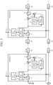
- FIG. 2 is a block diagram illustrating a configuration of a phase synchronization device according to a second embodiment.
- the phase synchronization device illustrated in FIG. 2 is a device including a plurality of elements, which are cascaded by a line 1a for transmitting and receiving signals to/from each other and a line 1b through which a reference signal from a reference signal source 1 propagates.
- An n-th element #n includes a PLL circuit 2, a directional coupler 3, a phase interpolator 4, a variable phase shifter 5, a directional coupler 6, a phase comparator 8, and a control circuit 9, receives input of a reference signal via the line 1b, and generates and outputs a signal with a phase ⁇ ⁇ ut_n .
- the phase synchronization device illustrated in FIG. 2 differs from the phase synchronization device according to the first embodiment in that the variable phase shifter 7 illustrated in FIG. 1 is not included and that the variable phase shifter 5 is disposed subsequent to the directional coupler 6, that is, between the directional coupler 6 and the subsequent element.
- the variable phase shifter 5 is a bidirectional phase shifter allowing bidirectional input and output.
- the PLL circuit 2 In the element #n, the PLL circuit 2 generates and outputs a first signal with a known frequency and a phase ⁇ n from the reference signal input via the line 1b.
- the phase interpolator 4 receives input of the first signal output from the PLL circuit 2 and a second signal with a phase shifted by the variable phase shifter 5, which is a bidirectional phase shifter included in the element #n-1, and generates and outputs a third signal having a phase ⁇ out_n that is intermediate between these signals.
- the directional coupler 6 outputs the third signal output from the phase interpolator 4 to the variable phase shifter 5.
- the variable phase shifter 5 outputs, as a second signal, a signal obtained by shifting the phase of the third signal input from the phase interpolator 4 via the directional coupler 6 by the phase shift amount ⁇ n to the element #n+1 via the line 1a.
- the phase comparator 8 receives input of the third signal having the phase ⁇ out_n output from the phase interpolator 4 and a fourth signal obtained by shifting the phase of a first signal output from the element #n+1 by the phase shift amount ⁇ n by the variable phase shifter 5, and detects a phase difference between these signals.
- the control circuit 9 controls the phase shift amount ⁇ n for the variable phase shifter 5 on the basis of the phase difference detected by the phase comparator 8. For example, the control circuit 9 determines a phase shift amount ⁇ n to reduce the phase difference detected by the phase comparator 8 to zero, and sets the determined phase shift amount ⁇ n in the variable phase shifter 5.
- the phase synchronization device includes the elements #1, #2,..., #n,... Because the element #n includes, as a phase shifter, the variable phase shifter 5 that is a bidirectional phase shifter, effects similar to those in the first embodiment can be produced. Furthermore, the bidirectional phase shifter enables the functions of the variable phase shifter 5 and the variable phase shifter 7 illustrated in FIG. 1 to be achieved by one phase shifter.
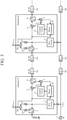
- FIG. 3 is a block diagram illustrating a configuration of a phase synchronization device according to a third embodiment.
- the phase synchronization device illustrated in FIG. 3 is a device including a plurality of elements, which are cascaded by the line 1a for transmitting and receiving signals to/from each other and a line 1b through which a reference signal from a reference signal source 1 propagates.
- An element #n includes a directional coupler 3, a phase interpolator 4, a variable phase shifter 5, a directional coupler 6, a variable phase shifter 7, a phase comparator 8, a control circuit 9, and a PLL circuit 11, receives input of a reference signal as a first signal via the line 1b, and generates and outputs a signal with an output phase ⁇ ⁇ ut_n .
- the first signal based on the reference signal input via the line 1b may be the reference signal itself.
- the phase synchronization device illustrated in FIG. 3 differs from the phase synchronization device according to the first embodiment in that the PLL circuit 2 illustrated in FIG. 1 is not included and that a PLL circuit 11 is included at the output of the phase interpolator 4.
- the directional coupler 3 included in element #n outputs the first signal, which is the reference signal input via the line 1b, to an element #n-1 via the line 1a.
- a phase rotation amount ⁇ 1 + ⁇ 2 + ⁇ 3 + ⁇ + ⁇ n-1 due to a wire delay is superimposed on the phase of the reference signal output from the element #n to the element #n-1.
- the phase interpolator 4 receives input of the first signal, which is the reference signal with the phase ⁇ n input from a reference signal source 1 via the line 1b, and a second signal with a phase shifted by a variable phase shifter 5 included in the element #n-1.
- the phase interpolator 4 generates a third signal having a phase that is intermediate between the first signal and the second signal, and outputs the third signal to the variable phase shifter 5, the phase comparator 8, and the PLL circuit 11.
- the PLL circuit 11 included in the element #n performs frequency multiplication on the third signal output from the phase interpolator 4 to generate a signal with a frequency higher than that of the reference signal and a phase ⁇ out_n , and outputs this signal as an output signal.
- the variable phase shifter 5 shifts the phase of the third signal output from the phase interpolator 4 by the phase shift amount ⁇ n , and outputs the third signal having a phase ⁇ out_n + ⁇ n to the directional coupler 6.
- the directional coupler 6 included in the element #n outputs, as a second signal, the third signal input from the variable phase shifter 5 to an element #n+1 via the line 1a. While the second signal propagates through the line 1a from the element #n to the element #n+1, a phase rotation amount ⁇ n due to a wire delay is added to the phase ⁇ out_n + ⁇ n of the second signal.
- the directional coupler 6 receives input of a first signal, which is a reference signal with a phase ⁇ n+1 output from a directional coupler 3 included in the subsequent element #n+1 from the element #n+1 via the line 1a, and outputs the first signal to the variable phase shifter 7. While the first signal propagates through the line 1a from the element #n+1 to the element #n, a phase rotation amount ⁇ n due to a wire delay is added to the phase of the first signal.
- a first signal which is a reference signal with a phase ⁇ n+1 output from a directional coupler 3 included in the subsequent element #n+1 from the element #n+1 via the line 1a
- variable phase shifter 7 shifts the phase of the first signal with a phase ⁇ n+1 + ⁇ n input from the element #n+1 via the line 1a and the directional coupler 6 by the phase shift amount ⁇ n to generate a fourth signal having a phase ⁇ n+1 + ⁇ n + ⁇ n .
- the fourth signal generated by the variable phase shifter 7 is output to the phase comparator 8.
- the phase comparator 8 receives input of the third signal output from the phase interpolator 4 and the fourth signal output from the variable phase shifter 7, and detects a phase difference between these signals. For example, the phase comparator 8 receives input of the third signal having the phase ⁇ out_n from the phase interpolator and the fourth signal having the phase ⁇ n+1 + ⁇ n + ⁇ n from the variable phase shifter 7, detects a phase difference between these signals and outputs the detected phase difference to the control circuit 9.
- the control circuit 9 determines a phase shift amount ⁇ n to reduce the phase difference detected by the phase comparator 8 to zero, and sets the phase shift amount ⁇ n in each of the variable phase shifter 5 and the variable phase shifter 7.
- the phase synchronization device includes the elements #1, #2,..., #n,...
- the phase interpolator 4 generates the third signal by using the reference signal with the phase ⁇ n input via the line 1b, and the PLL circuit 11 performs frequency multiplication on the third signal output from the phase interpolator 4 to generate the output signal.
- the frequency with which phase synchronization is performed is the frequency of the reference signal, and because the frequency of the reference signal is lower than the frequency of the signal on which frequency multiplication is performed by the PLL circuit, attenuation of a signal output from a previous element is reduced.
- the third embodiment can also be applied to the configuration of the elements presented in the second embodiment.
- the elements included in the phase synchronization device according to the third embodiment may each have a configuration in which the variable phase shifter 7 is not included and the PLL circuit 2 in the elements illustrated in FIG. 2 is replaced by the PLL circuit 11.
- Such a configuration can also produce effects similar to those of the first and third embodiments.
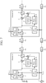
- FIG. 4 is a block diagram illustrating a configuration of a phase synchronization device according to a fourth embodiment.
- the phase synchronization device illustrated in FIG. 4 is a device including a plurality of elements, which are cascaded by a line 1b through which a reference signal from a reference signal source 1, and transmits and receives signals to/from each other by radio transmission using antennas 12 and antennas 13.
- An element #n includes a directional coupler 3, a phase interpolator 4, a variable phase shifter 5, a directional coupler 6, a variable phase shifter 7, a phase comparator 8, a control circuit 9, and a PLL circuit 2, receives a reference signal via a line 1b, and generates and outputs a signal with a phase ⁇ ⁇ ut_n .
- the directional coupler 3 included in the element #n transmits a first signal with a phase ⁇ n input from the PLL circuit 2 to an element #n-1 via an antenna 12.
- a directional coupler 6 included in the element #n-1 receives the first signal from the element #n via an antenna 13. Radio waves radiated from the antennas 12 and the antennas 13 experience phase rotation when propagating through space. Thus, phase rotation amounts ⁇ 1 , ⁇ 2 ,..., ⁇ n ,... are superimposed on signals transmitted and received to/from the elements via the antennas 12 and the antennas 13.
- phase synchronization device operates in a manner similar to the first embodiment except that signals are transmitted and received to/from the elements via the antennas 12 and the antennas 13.
- each of the elements has the configuration illustrated in FIG. 1 , includes an antenna 12 and an antenna 13, and transmits and receives signals to/from each other by radio communication via the antenna 12 and the antenna 13.
- FIG. 1 each of the elements has the configuration illustrated in FIG. 1 , includes an antenna 12 and an antenna 13, and transmits and receives signals to/from each other by radio communication via the antenna 12 and the antenna 13.
- the fourth embodiment can be applied to the configuration of the elements presented in the second embodiment and to the configuration of the elements presented in the third embodiment.
- the elements included in the phase synchronization device according to the fourth embodiment may each have a configuration in which an antenna 12 and an antenna 13 are included in each of the elements illustrated in FIG. 2 .
- This configuration can also produce effects similar to those of the first, second, and fourth embodiments.
- the elements included in the phase synchronization device according to the fourth embodiment may each have a configuration in which an antenna 12 and an antenna 13 are included in each of the elements illustrated in FIG. 3 . This configuration can also produce effects similar to those of the first, third, and fourth embodiments.
- FIG. 5 is a block diagram illustrating a configuration of a phase synchronization device according to a fifth embodiment, and illustrates a specific configuration of a phase interpolator included in each element.
- FIG. 6 is a block diagram illustrating a configuration of the phase interpolator in the fifth embodiment, in which only the configuration of the phase interpolator in each of the elements of the phase synchronization device of FIG. 5 is illustrated.
- the phase interpolator according to the fifth embodiment include an amplifier 14, an amplifier 15, and an adder 16 as illustrated in FIGS. 5 and 6 .
- the amplifier 14 is a first amplifier that amplifies one (input (1) in FIG. 6 ; first signal) of two signals input to the phase interpolator to have the same amplitude as the amplifier 15, and outputs the amplified signal "a".
- the amplifier 15 is a second amplifier that amplifies the other (input (2) in FIG. 6 ; second signal) of the two signals input to the phase interpolator to have the same amplitude as the amplifier 14, and outputs the amplified signal "b".
- the signal "a” amplified by the amplifier 14 and the signal "b” amplified by the amplifier 15 are output to the adder 16.
- the amplifier 14 and the amplifier 15 can be implemented by limiter amplifiers or variable gain amplifiers (VGAs).
- the adder 16 is a first adder that adds the signal "a" output from the amplifier 14 and the signal “b” output from the amplifier 15, and outputs a signal (output in FIG. 6 ) resulting from the addition.
- the phase of the signal "a” is ⁇ 1
- the signal “a” can be expressed by sin( ⁇ t+ ⁇ 1 ) by using an angular velocity co and time t.
- the phase of the signal "b” is ⁇ 2
- the signal “b” can be expressed by sin( ⁇ t+ ⁇ 2 ) by using an angular velocity co and time t.
- the signal obtained by adding the signal "a” and the signal “b” by the adder 16 can be expressed by the following formula (1).
- 2cos ⁇ ( ⁇ 1 - ⁇ 2 )/2 ⁇ expresses the gain of the output signal of the adder 16.
- sin[ ⁇ t + ⁇ ( ⁇ 1 + ⁇ 2 )/2 ⁇ ] expresses the phase of the output signal of the adder 16, and the output phase is an average of the phases of the signal "a" input to the amplifier 14 and the signal "b" input to the amplifier 15.
- each of the elements includes the phase interpolator constituted by the amplifier 14, the amplifier 15, and the adder 16. This configuration enables phase synchronization even when signals transmitted and received to/from the elements have different amplitudes from each other.
- phase synchronization device in which each of the phase interpolators 4 illustrated in FIG. 1 is replaced by the phase interpolator illustrated in FIG. 6 is presented in the description above.
- the phase synchronization device according to the fifth embodiment may be a device in which each of the phase interpolators 4 presented in any of the second to fourth embodiments is replaced by the phase interpolator illustrated in FIG. 6 , which can produce effects similar to those described above.
- FIG. 7 is a block diagram illustrating a configuration of a phase synchronization device according to a sixth embodiment, in which each element includes a phase interpolator 17.
- FIG. 8 is a block diagram illustrating a configuration of the phase interpolator 17, and illustrates an internal configuration of the phase interpolator 17. As illustrated in FIG. 8 , the phase interpolator 17 includes a phase comparator 17a, a phase comparator 17b, an adder 17c, a loop filter 17d, and a frequency variable oscillation circuit 17e.
- the phase comparator 17a is a first phase comparator that detects a phase difference between one (first signal) of two signals input to the phase interpolator 17 and an output signal generated by the frequency variable oscillation circuit 17e, and outputs a signal proportional to the detected phase difference.
- the one signal is a reference signal with a phase ⁇ ref1 .
- the reference signal with the phase ⁇ ref1 is input to the phase comparator 17a, and the output signal generated by the frequency variable oscillation circuit 17e is further returned to the input of the phase comparator 17a.
- the phase comparator 17b is a second phase comparator that detects a phase difference between the other (second signal) of the two signals input to the phase interpolator 17 and an output signal generated by the frequency variable oscillation circuit 17e, and outputs a signal proportional to the detected phase difference.
- the other signal is a reference signal with a phase ⁇ ref2 different from ⁇ ref1 .
- the reference signal with the phase ⁇ ref2 is input to the phase comparator 17b, and the output signal generated by the frequency variable oscillation circuit 17e is further returned to the input of the phase comparator 17b.
- the adder 17c is a second adder that adds a signal output from the phase comparator 17a and a signal output from the phase comparator 17b. A signal resulting from the addition by the adder 17c is output to the loop filter 17d.
- the loop filter 17d smooths the signal resulting from the addition by the adder 17c, and outputs the smoothed signal to the frequency variable oscillation circuit 17e.
- the frequency variable oscillation circuit 17e is a first frequency variable oscillation circuit that generates an output signal of the phase interpolator 17.
- the frequency variable oscillation circuit 17e changes the frequency of the output signal of the phase interpolator 17 on the basis of the signal smoothed by the loop filter 17d.
- the signal output from the phase interpolator 17 is a signal having a phase that is intermediate between the reference signals.
- the phase interpolator 17 includes the phase comparator 17a, the phase comparator 17b, the adder 17c, the loop filter 17d, and the frequency variable oscillation circuit 17e.
- the phase interpolation accuracy is determined by the comparison accuracies of the phase comparator 17a and the phase comparator 17b, and the phase synchronization device according to the sixth embodiment thus produces an effect of increasing the accuracy of phase interpolation more easily than the phase synchronization device presented in the fifth embodiment.
- phase synchronization device in which each of the phase interpolators 4 illustrated in FIG. 1 is replaced by the phase interpolator 17 illustrated in FIG. 8 is presented in the description above.
- the phase synchronization device according to the sixth embodiment may be a device in which each of the phase interpolators 4 included in the phase synchronization device illustrated in the second to fourth embodiments is replaced by the phase interpolator 17, which can produce effects similar to those described above.
- FIG. 9 is a block diagram illustrating a configuration of a phase synchronization device according to a seventh embodiment.
- the phase synchronization device illustrated in FIG. 9 has a configuration similar to that of the phase synchronization device illustrated in FIG. 3 , but each of the elements does not include the PLL circuit 11 illustrated in FIG. 3 , and the phase interpolator 4 is replaced by a phase interpolator 18.
- an output of a frequency divider 18f included in the phase interpolator 18 is given to the variable phase shifter 5 and the phase comparator 8.
- An output signal of each of the elements is an output signal of the phase interpolator 18.
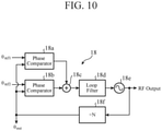
- FIG. 10 is a block diagram illustrating a configuration of the phase interpolator 18, and illustrates an internal configuration of the phase interpolator 18.
- the phase interpolator 18 includes a phase comparator 18a, a phase comparator 18b, an adder 18c, a loop filter 18d, a frequency variable oscillation circuit 18e, and the frequency divider 18f. Note that, the frequency divider 18f is described as " ⁇ N" in FIG. 10 .
- the phase comparator 18a is a third phase comparator that detects a phase difference between one of two signals input to the phase interpolator 18 and an output signal generated by the frequency variable oscillation circuit 18e, and outputs a signal proportional to the detected phase difference.
- the one signal is a reference signal with a phase ⁇ ref1 .
- the reference signal with the phase ⁇ ref1 is input to the phase comparator 18a, and the output signal generated by the frequency variable oscillation circuit 18e is further returned to the input of the phase comparator 18a.
- the phase comparator 18b is a fourth phase comparator that detects a phase difference between the other of two signals input to the phase interpolator 18 and an output signal generated by the frequency variable oscillation circuit 18e, and outputs a signal proportional to the detected phase difference.
- the other signal is a reference signal with a phase ⁇ ref2 different from ⁇ ref1 .
- the reference signal with the phase ⁇ ref2 is input to the phase comparator 18b, and the output signal generated by the frequency variable oscillation circuit 18e is further returned to the input of the phase comparator 18b.
- the adder 18c is a third adder that adds a signal output from the phase comparator 18a and a signal output from the phase comparator 18b. A signal resulting from the addition by the adder 18c is output to the loop filter 18d.
- the loop filter 18d smooths the signal output from the adder 18c, and outputs the smoothed signal to the frequency variable oscillation circuit 18e.
- the frequency variable oscillation circuit 18e is a second frequency variable oscillation circuit that generates an output signal of the phase interpolator 18. In addition, the frequency variable oscillation circuit 18e changes the frequency of the output signal of the phase interpolator 18 on the basis of the signal smoothed by the loop filter 18d.
- the frequency divider 18f is a frequency divider that divides the frequency of the output signal generated by the frequency variable oscillation circuit 18e.
- the output signal of the frequency variable oscillation circuit 18e is divided in frequency by the frequency divider 18f, and then returned to the inputs of the phase comparator 18a and the phase comparator 18b.
- the phase interpolator 18 includes the phase comparator 18a, the phase comparator 18b, the adder 18c, the loop filter 18d, the frequency variable oscillation circuit 18e, and the frequency divider 18f. Because the phase interpolator 18 can perform phase interpolation and frequency multiplication on the two input reference signals (phases ⁇ ref1 and ⁇ ref2 ) at the same time, the phase synchronization device according to the seventh embodiment produces an effect of enabling reduction in power consumption as compared with the phase synchronization device presented in the sixth embodiment.
- phase synchronization device in which each of the phase interpolators 4 illustrated in FIG. 3 is replaced by the phase interpolator 18 illustrated in FIG. 10 is presented in the description above.
- the phase synchronization device according to the seventh embodiment may be a device in which each of the phase interpolators 4 included in the phase synchronization devices presented in the first, second, and fourth embodiments is replaced with the phase interpolator 18, the PLL circuits 2 are further deleted, and the output of each of the frequency dividers is given to the variable phase shifter 5 and the phase comparator 8, which can produce effects similar to those described above.
- a phase synchronization device can make the phases of signals output from a plurality of elements equal to each other, and can thus be used for an APAA.
Landscapes
- Physics & Mathematics (AREA)
- General Physics & Mathematics (AREA)
- Engineering & Computer Science (AREA)
- Computational Mathematics (AREA)
- Mathematical Analysis (AREA)
- Pure & Applied Mathematics (AREA)
- Theoretical Computer Science (AREA)
- Computing Systems (AREA)
- Mathematical Optimization (AREA)
- General Engineering & Computer Science (AREA)
- Stabilization Of Oscillater, Synchronisation, Frequency Synthesizers (AREA)
- Synchronisation In Digital Transmission Systems (AREA)
Abstract
Description
- The present invention relates to a phase synchronization device including a plurality of cascaded elements.
- For example, a phase synchronization device including a plurality of elements with output phases equal to each other may be used for an active phased array antenna (APAA) or a very large scale integration (VLSI). Each of the elements detects a phase difference between the phase of a reference signal and the phase of a signal that is referred to, returns the phases so that the detected phase difference is 0, and can thus output a signal with a stable frequency.
- Note that, when the number of elements increases, it is difficult to distribute the reference signal to the individual elements with an equal path length, and a phase rotation amount (referred to as a phase rotation amount A) due to the difference between the path lengths is added to the output phase of each of the elements. Furthermore, the phase rotation amounts (referred to as phase rotation amounts B) caused in the elements vary depending on the gains depending on the elements. As a result, the output phases of the elements may be deviated from each other.
- For example, a phase synchronization device described in
Non-patent Literature 1 detects and returns a phase difference between elements caused by the phase rotation amounts A and B to correct the phase difference between the output phases of the elements. - Non-patent Literature 1: Toshihiro Shimura, Takenori Ohshima, Hiroshi Ashida, Shohei Ishikawa, Shunsuke Fujio, Atsushi Honda, Zhengyi Li, Kenichi Nishikawa, Chikara Kojima, Kazuyuki Ozaki, Masahiko Shimizu and Yoji Ohashi, "Millimeter-Wave TX Phased Array with Phase Adjusting Function between Transmitters for Hybrid Beamforming with Interleaved Subarrays", Proceedings of the 46th European Microwave Conference, October 2016, pp. 1572-1575.
- In the phase synchronization device described in
Non-patent Literature 1, the elements are connected by lines for transmitting and receiving signals for synchronization of the output phases between the elements. Thus, in the phase synchronization device described inNon-patent Literature 1, phase rotation amounts (referred to as phase rotation amounts C) due to wire delays through the lines connecting the elements are caused in addition to the phase rotation amounts A and B, and these amounts cannot be distinguished from each other. Thus, in a case where the phase rotation amounts C have changed in addition to the phase rotation amounts A and the phase rotation amounts B by changes in environmental conditions, for example, there is a problem in that the phase differences between the output phases of the elements cannot be accurately corrected, and the output phases of the elements are not equal to each other. - The present invention has been made to solve the aforementioned problem, and an object thereof is to provide a phase synchronization device capable of making output phases of a plurality of elements equal to each other.
- A phase synchronization device according to the present invention is a phase synchronization device including a plurality of cascaded elements, the elements each including a phase interpolator, a phase shifter, a phase comparator, and a control circuit, wherein the phase interpolator receives input of a first signal based on a reference signal input via a line and a second signal output from the phase shifter included in an element of a previous stage, and generates and outputs a third signal having a phase intermediate between the first signal and the second signal, the phase shifter outputs, as the second signal, the third signal with a phase shifted by a first phase shift amount to the phase interpolator included in an element of a subsequent stage, the phase comparator detects a phase difference between the third signal and a fourth signal obtained by shifting a phase of the first signal output from the element of the subsequent stage by the first phase shift amount, and the control circuit controls the first phase shift amount for the phase shifter on a basis of the phase difference detected by the phase comparator.
- According to the present invention, a third signal having a phase intermediate between a first signal based on a reference signal and a second signal phase shifted by an element of a previous stage is generated, a signal obtained by shifting the phase of the third signal by a first phase shift amount is output as a second signal to an element of a subsequent stage, a phase difference between the third signal and a fourth signal obtained by shifting the phase of a first signal output from the element of the subsequent stage by the first phase shift amount is detected, and the first phase shift amount is controlled on the basis of the detected phase difference. As a result, output phases of a plurality elements can be made equal to each other.
-
-
FIG. 1 is a block diagram illustrating a configuration of a phase synchronization device according to a first embodiment. -
FIG. 2 is a block diagram illustrating a configuration of a phase synchronization device according to a second embodiment. -
FIG. 3 is a block diagram illustrating a configuration of a phase synchronization device according to a third embodiment. -
FIG. 4 is a block diagram illustrating a configuration of a phase synchronization device according to a fourth embodiment. -
FIG. 5 is a block diagram illustrating a configuration of a phase synchronization device according to a fifth embodiment. -
FIG. 6 is a block diagram illustrating a configuration of a phase interpolator according to the fifth embodiment. -
FIG. 7 is a block diagram illustrating a configuration of a phase synchronization device according to a sixth embodiment. -
FIG. 8 is a block diagram illustrating a configuration of a phase interpolator according to the sixth embodiment. -
FIG. 9 is a block diagram illustrating a configuration of a phase synchronization device according to a seventh embodiment. -
FIG. 10 is a block diagram illustrating a configuration of a phase interpolator according to the seventh embodiment. -
FIG. 1 is a block diagram illustrating a configuration of a phase synchronization device according to a first embodiment. The phase synchronization device illustrated inFIG. 1 is a device including a plurality of elements, which are cascaded by a line 1a for transmitting and receiving signals to/from each other and aline 1b through which a reference signal from areference signal source 1 propagates. An n-th element #n (n = 1, 2,...) includes a PLL circuit 2 (phase synchronization circuit), adirectional coupler 3, a phase interpolator 4, avariable phase shifter 5, adirectional coupler 6, a variable phase shifter 7, aphase comparator 8, and acontrol circuit 9, receives input of a reference signal via theline 1b, and generates and outputs a signal with a phase θοut_n. - The
PLL circuit 2 generates and outputs a first signal based on the reference signal input via theline 1b. For example, thePLL circuit 2 performs frequency multiplication of the reference signal to output a signal with a known frequency (a signal with a radio frequency (RF)) higher than the frequency of the reference signal. Note that a phase rotation amount β1+β2+β3+...+βn-1 due to a wire delay is added to the phase of the reference signal input through theline 1b. Thus, the phase θn of the first signal includes the phase rotation amount generated in the element #n and the phase rotation amount of the reference signal due to the wire delay. - The first signal with the phase θn generated by the
PLL circuit 2 is output to thedirectional coupler 3 and the phase interpolator 4. Thedirectional coupler 3 included in the element #n outputs the first signal to a previous ((n-1)-th) element #n-1 via the line 1a. While the first signal propagates through the line 1a from the element #n to the element #n-1, a phase rotation amount αn-1 due to a wire delay is added to the phase θn of the first signal. In addition, thedirectional coupler 3 receives input of a second signal with a phase shifted by avariable phase shifter 5 included in the previous element #n-1 via the same line 1a, and outputs the second signal to the phase interpolator 4. While the second signal propagates through the line 1a from the element #n-1 to the element #n, a phase rotation amount αn-1 due to a wire delay is added to the phase of the second signal. - The phase interpolator 4 included in the element #n receives input of the first signal with the phase θn output from the
PLL circuit 2 and the second signal with the phase shifted in the element #n-1, and generates a third signal having a phase θout_n that is intermediate between these signals. The third signal is output as an output signal from the element #n. Furthermore, the third signal generated by the phase interpolator 4 is also output to thevariable phase shifter 5 and thephase comparator 8. - The
variable phase shifter 5 is a first phase shifter that shifts the phase of an input signal by a phase shift amount γn, which is a first phase shift amount, controlled by thecontrol circuit 9. The variable phase shifter 5 shifts the phase of the third signal output from the phase interpolator 4 by the phase shift amount γn, and outputs the third signal having a phase θout_n+γn to thedirectional coupler 6. Thedirectional coupler 6 included in the element #n outputs, as a second signal, the third signal input from thevariable phase shifter 5 to an element #n+1 via the line 1a. While the second signal propagates through the line 1a from the element #n to the element #n+1, a phase rotation amount αn due to a wire delay is added to the phase θout_n+γn of the second signal. - The
directional coupler 6 receives input of a first signal, which is a signal with a phase θn+1 output from aPLL circuit 2 included in the element #n+1, from the element #n+1 via the line 1a, and outputs the first signal to the variable phase shifter 7. While the first signal propagates through the line 1a from the element #n+1 to the element #n, a phase rotation amount αn due to a wire delay is added to the phase of the first signal. - The variable phase shifter 7 is a second phase shifter that shifts the phase of an input signal by the same phase shift amount γn as that of the
variable phase shifter 5, and the phase shift amount γn is controlled by thecontrol circuit 9. The variable phase shifter 7 receives input of the first signal with the phase θn+1+αn from the element #n+1 via the line 1a and thedirectional coupler 6, and shifts the phase of the first signal by the phase shift amount γn to generate a fourth signal having a phase θn+1+αn+γn. The fourth signal generated by the variable phase shifter 7 is output to thephase comparator 8. - The
phase comparator 8 receives input of the third signal output from the phase interpolator 4 and the fourth signal output from the variable phase shifter 7, and detects a phase difference between these signals. For example, thephase comparator 8 receives input of the third signal having the phase θout_n from the phase interpolator 4 and the fourth signal having the phase θn+1+αn+γn from the variable phase shifter 7, detects a phase difference between the input signals and outputs the detected phase difference to thecontrol circuit 9. - The
control circuit 9 controls the phase shift amount γn for thevariable phase shifter 5 and the variable phase shifter 7 on the basis of the phase difference detected by thephase comparator 8. For example, thecontrol circuit 9 determines a phase shift amount γn to reduce the phase difference detected by thephase comparator 8 to zero, and sets the determined phase shift amount γn in each of thevariable phase shifter 5 and the variable phase shifter 7. - Next, operation of the phase synchronization device according to the first embodiment will be described.
- The phase θout_n of the output signal (third signal) output from the element #n is made to be θout_n = θn+1+αn+γn by the
phase comparator 8 and thecontrol circuit 9 included in the element #n. In addition, as a result of similar operation in the previous element #n-1, the phase θout_n-1 of the output signal (third signal) output from the element #n-1 is θout_n-1 = θn+αn-1+γn-1. Furthermore, the phase interpolator 4 included in the element #n receives input of the first signal with the phase θn output from thePLL circuit 2 and the second signal having a phase θout_n-1+αn-1+γn-1 from the element #n-1 input by thedirectional coupler 3. - The phase interpolator 4 generates and outputs the third signal having a phase θout_n that is intermediate between the phase θout_n-1+αn-1+γn-1 and the phase θn. The phase θout_n of the third signal is θout_n = (θout_n-1+αn-1+γn-1 + θn)/2.
- On the basis of θout_n-1 = θn+αn-1+γn-1, the output phase θout_n is θout_n = θout_n-1, and thus the output phase of the element #n-1 is the same as that of the element #n.
- In contrast, a connection terminal for connection with a previous stage is terminated at the phase interpolator 4 included in a
first element # 1 because no previous element is present as illustrated inFIG. 1 . Thus, no second signal from thedirectional coupler 3 is input to the phase interpolator 4 included in thefirst element # 1. When no signal is input to one of the two inputs of the phase interpolator 4, the output phase is dependent only on the phase of the other of the two inputs. Thus, the output phase θout_1 of the phase interpolator 4 included in theelement # 1 is determined only by the phase θ1 of a signal input from thePLL circuit 2. As a result, output phases θout_1, θout_2, θout_3,..., θout_n,... are all equal to θout_1. - In addition, the order in which the operations of individual components settle is as follows.
- First, the
PLL circuit 2 included in theelement # 1 locks, and the output phase θ1 thereof is determined. - Because the output phase θout_1 of the
element # 1 is dependent only on the phase θ1 of the first signal generated by thePLL circuit 2, the output phase θout_1 is settled at this point. Subsequently, after the output phase of thePLL circuit 2 included in theelement # 2 is settled at θ2, the operations of thevariable phase shifter 5, the variable phase shifter 7, thephase comparator 8, and thecontrol circuit 9 included in theelement # 1 are settled, and the phase shift amount γ1 is determined. In this manner, the output phase θout_2 of theelement # 2 is settled. Thereafter, the output phases θout_3, θout_4,..., θout_n,... settle through similar procedures. - As described above, the phase synchronization device according to the first embodiment includes the
elements # 1, #2,..., #n,... In the element #n, the third signal having a phase that is intermediate between the first signal based on the reference signal input via theline 1b and the second signal output from the element #n-1 is generated, a signal obtained by shifting the phase of the third signal by the phase shift amount γn is output as a second signal to the element #n+1, the phase difference between the third signal and the fourth signal, which is obtained by shifting a first signal output from the element #n+1 by the phase shift amount γn, is detected, and the phase shift amount γn is controlled on the basis of the detected phase difference. - As a result, the phase synchronization device according to the first embodiment can make the output phases of a plurality of elements equal to each other independently of all of the phase rotation amount βn due to a wire delay caused by a path difference of the
line 1b depending on each element, the phase θn including the phase rotation amount generated in the element #n, and the phase rotation amount αn due to a wire delay of the line 1a. -
FIG. 2 is a block diagram illustrating a configuration of a phase synchronization device according to a second embodiment. The phase synchronization device illustrated inFIG. 2 is a device including a plurality of elements, which are cascaded by a line 1a for transmitting and receiving signals to/from each other and aline 1b through which a reference signal from areference signal source 1 propagates. - An n-th element #n includes a
PLL circuit 2, adirectional coupler 3, a phase interpolator 4, avariable phase shifter 5, adirectional coupler 6, aphase comparator 8, and acontrol circuit 9, receives input of a reference signal via theline 1b, and generates and outputs a signal with a phase θοut_n. - The phase synchronization device illustrated in
FIG. 2 differs from the phase synchronization device according to the first embodiment in that the variable phase shifter 7 illustrated inFIG. 1 is not included and that thevariable phase shifter 5 is disposed subsequent to thedirectional coupler 6, that is, between thedirectional coupler 6 and the subsequent element. In addition, thevariable phase shifter 5 is a bidirectional phase shifter allowing bidirectional input and output. - In the element #n, the
PLL circuit 2 generates and outputs a first signal with a known frequency and a phase θn from the reference signal input via theline 1b. The phase interpolator 4 receives input of the first signal output from thePLL circuit 2 and a second signal with a phase shifted by thevariable phase shifter 5, which is a bidirectional phase shifter included in the element #n-1, and generates and outputs a third signal having a phase θout_n that is intermediate between these signals. Thedirectional coupler 6 outputs the third signal output from the phase interpolator 4 to thevariable phase shifter 5. Thevariable phase shifter 5 outputs, as a second signal, a signal obtained by shifting the phase of the third signal input from the phase interpolator 4 via thedirectional coupler 6 by the phase shift amount γn to the element #n+1 via the line 1a. - The
phase comparator 8 receives input of the third signal having the phase θout_n output from the phase interpolator 4 and a fourth signal obtained by shifting the phase of a first signal output from the element #n+1 by the phase shift amount γn by thevariable phase shifter 5, and detects a phase difference between these signals. Thecontrol circuit 9 controls the phase shift amount γn for thevariable phase shifter 5 on the basis of the phase difference detected by thephase comparator 8. For example, thecontrol circuit 9 determines a phase shift amount γn to reduce the phase difference detected by thephase comparator 8 to zero, and sets the determined phase shift amount γn in thevariable phase shifter 5. - As described above, the phase synchronization device according to the second embodiment includes the
elements # 1, #2,..., #n,... Because the element #n includes, as a phase shifter, thevariable phase shifter 5 that is a bidirectional phase shifter, effects similar to those in the first embodiment can be produced. Furthermore, the bidirectional phase shifter enables the functions of thevariable phase shifter 5 and the variable phase shifter 7 illustrated inFIG. 1 to be achieved by one phase shifter. -
FIG. 3 is a block diagram illustrating a configuration of a phase synchronization device according to a third embodiment. The phase synchronization device illustrated inFIG. 3 is a device including a plurality of elements, which are cascaded by the line 1a for transmitting and receiving signals to/from each other and aline 1b through which a reference signal from areference signal source 1 propagates. An element #n includes adirectional coupler 3, a phase interpolator 4, avariable phase shifter 5, adirectional coupler 6, a variable phase shifter 7, aphase comparator 8, acontrol circuit 9, and aPLL circuit 11, receives input of a reference signal as a first signal via theline 1b, and generates and outputs a signal with an output phase θοut_n. Thus, the first signal based on the reference signal input via theline 1b may be the reference signal itself. - The phase synchronization device illustrated in
FIG. 3 differs from the phase synchronization device according to the first embodiment in that thePLL circuit 2 illustrated inFIG. 1 is not included and that aPLL circuit 11 is included at the output of the phase interpolator 4. In addition, thedirectional coupler 3 included in element #n outputs the first signal, which is the reference signal input via theline 1b, to an element #n-1 via the line 1a. Thus, a phase rotation amount β1+β2+β3+···+βn-1 due to a wire delay is superimposed on the phase of the reference signal output from the element #n to the element #n-1. - The phase interpolator 4 receives input of the first signal, which is the reference signal with the phase θn input from a
reference signal source 1 via theline 1b, and a second signal with a phase shifted by avariable phase shifter 5 included in the element #n-1. The phase interpolator 4 generates a third signal having a phase that is intermediate between the first signal and the second signal, and outputs the third signal to thevariable phase shifter 5, thephase comparator 8, and thePLL circuit 11. ThePLL circuit 11 included in the element #n performs frequency multiplication on the third signal output from the phase interpolator 4 to generate a signal with a frequency higher than that of the reference signal and a phase θout_n, and outputs this signal as an output signal. - The
variable phase shifter 5 shifts the phase of the third signal output from the phase interpolator 4 by the phase shift amount γn, and outputs the third signal having a phase θout_n+γn to thedirectional coupler 6. Thedirectional coupler 6 included in the element #n outputs, as a second signal, the third signal input from thevariable phase shifter 5 to an element #n+1 via the line 1a. While the second signal propagates through the line 1a from the element #n to the element #n+1, a phase rotation amount αn due to a wire delay is added to the phase θout_n+γn of the second signal. - In addition, the
directional coupler 6 receives input of a first signal, which is a reference signal with a phase θn+1 output from adirectional coupler 3 included in the subsequent element #n+1 from the element #n+1 via the line 1a, and outputs the first signal to the variable phase shifter 7. While the first signal propagates through the line 1a from the element #n+1 to the element #n, a phase rotation amount αn due to a wire delay is added to the phase of the first signal. - The variable phase shifter 7 shifts the phase of the first signal with a phase θn+1+αn input from the element #n+1 via the line 1a and the
directional coupler 6 by the phase shift amount γn to generate a fourth signal having a phase θn+1+αn+γn. The fourth signal generated by the variable phase shifter 7 is output to thephase comparator 8. - The
phase comparator 8 receives input of the third signal output from the phase interpolator 4 and the fourth signal output from the variable phase shifter 7, and detects a phase difference between these signals. For example, thephase comparator 8 receives input of the third signal having the phase θout_n from the phase interpolator and the fourth signal having the phase θn+1+αn+γn from the variable phase shifter 7, detects a phase difference between these signals and outputs the detected phase difference to thecontrol circuit 9. Thecontrol circuit 9 determines a phase shift amount γn to reduce the phase difference detected by thephase comparator 8 to zero, and sets the phase shift amount γn in each of thevariable phase shifter 5 and the variable phase shifter 7. - As described above, the phase synchronization device according to the third embodiment includes the
elements # 1, #2,..., #n,... In the element #n, the phase interpolator 4 generates the third signal by using the reference signal with the phase θn input via theline 1b, and thePLL circuit 11 performs frequency multiplication on the third signal output from the phase interpolator 4 to generate the output signal. As a result, effects similar to those of the first embodiment can be produced. In addition, in theelements # 1, #2,..., #n,..., the frequency with which phase synchronization is performed is the frequency of the reference signal, and because the frequency of the reference signal is lower than the frequency of the signal on which frequency multiplication is performed by the PLL circuit, attenuation of a signal output from a previous element is reduced. - While the configuration in which the
PLL circuit 2 in each of the elements illustrated inFIG. 1 is replaced by thePLL circuit 11 is presented in the description above, the third embodiment can also be applied to the configuration of the elements presented in the second embodiment. For example, the elements included in the phase synchronization device according to the third embodiment may each have a configuration in which the variable phase shifter 7 is not included and thePLL circuit 2 in the elements illustrated inFIG. 2 is replaced by thePLL circuit 11. Such a configuration can also produce effects similar to those of the first and third embodiments. -
FIG. 4 is a block diagram illustrating a configuration of a phase synchronization device according to a fourth embodiment. The phase synchronization device illustrated inFIG. 4 is a device including a plurality of elements, which are cascaded by aline 1b through which a reference signal from areference signal source 1, and transmits and receives signals to/from each other by radiotransmission using antennas 12 andantennas 13. An element #n includes adirectional coupler 3, a phase interpolator 4, avariable phase shifter 5, adirectional coupler 6, a variable phase shifter 7, aphase comparator 8, acontrol circuit 9, and aPLL circuit 2, receives a reference signal via aline 1b, and generates and outputs a signal with a phase θοut_n. - The
directional coupler 3 included in the element #n transmits a first signal with a phase θn input from thePLL circuit 2 to an element #n-1 via anantenna 12. Adirectional coupler 6 included in the element #n-1 receives the first signal from the element #n via anantenna 13. Radio waves radiated from theantennas 12 and theantennas 13 experience phase rotation when propagating through space. Thus, phase rotation amounts α1, α2,..., αn,... are superimposed on signals transmitted and received to/from the elements via theantennas 12 and theantennas 13. - Note that the phase synchronization device according to the fourth embodiment operates in a manner similar to the first embodiment except that signals are transmitted and received to/from the elements via the
antennas 12 and theantennas 13. - As described above, in the phase synchronization device according to the fourth embodiment, each of the elements has the configuration illustrated in
FIG. 1 , includes anantenna 12 and anantenna 13, and transmits and receives signals to/from each other by radio communication via theantenna 12 and theantenna 13. As a result, effects similar to those of the first embodiment can be produced. Furthermore, in the fourth embodiment, because signals are transmitted and received to/from each other by radio communication, phase synchronization can be performed even when elements are spatially away from each other. - While the configuration in which the
antennas 12 and theantennas 13 are introduced in the elements illustrated inFIG. 1 is presented in the description above, the fourth embodiment can be applied to the configuration of the elements presented in the second embodiment and to the configuration of the elements presented in the third embodiment. - For example, the elements included in the phase synchronization device according to the fourth embodiment may each have a configuration in which an
antenna 12 and anantenna 13 are included in each of the elements illustrated inFIG. 2 . This configuration can also produce effects similar to those of the first, second, and fourth embodiments. Furthermore, the elements included in the phase synchronization device according to the fourth embodiment may each have a configuration in which anantenna 12 and anantenna 13 are included in each of the elements illustrated inFIG. 3 . This configuration can also produce effects similar to those of the first, third, and fourth embodiments. -
FIG. 5 is a block diagram illustrating a configuration of a phase synchronization device according to a fifth embodiment, and illustrates a specific configuration of a phase interpolator included in each element.FIG. 6 is a block diagram illustrating a configuration of the phase interpolator in the fifth embodiment, in which only the configuration of the phase interpolator in each of the elements of the phase synchronization device ofFIG. 5 is illustrated. The phase interpolator according to the fifth embodiment include anamplifier 14, anamplifier 15, and anadder 16 as illustrated inFIGS. 5 and6 . - The
amplifier 14 is a first amplifier that amplifies one (input (1) inFIG. 6 ; first signal) of two signals input to the phase interpolator to have the same amplitude as theamplifier 15, and outputs the amplified signal "a". Theamplifier 15 is a second amplifier that amplifies the other (input (2) inFIG. 6 ; second signal) of the two signals input to the phase interpolator to have the same amplitude as theamplifier 14, and outputs the amplified signal "b". The signal "a" amplified by theamplifier 14 and the signal "b" amplified by theamplifier 15 are output to theadder 16. Theamplifier 14 and theamplifier 15 can be implemented by limiter amplifiers or variable gain amplifiers (VGAs). - The
adder 16 is a first adder that adds the signal "a" output from theamplifier 14 and the signal "b" output from theamplifier 15, and outputs a signal (output inFIG. 6 ) resulting from the addition. When the phase of the signal "a" is θ1, the signal "a" can be expressed by sin(ωt+θ1) by using an angular velocity co and time t. Similarly, when the phase of the signal "b" is θ2, the signal "b" can be expressed by sin(ωt+θ2) by using an angular velocity co and time t. The signal obtained by adding the signal "a" and the signal "b" by theadder 16 can be expressed by the following formula (1).
- In the formula (1), 2cos{(θ1-θ2)/2} expresses the gain of the output signal of the
adder 16. In addition, sin[ωt + {(θ1+θ2)/2}] expresses the phase of the output signal of theadder 16, and the output phase is an average of the phases of the signal "a" input to theamplifier 14 and the signal "b" input to theamplifier 15. - As described above, in the phase synchronization device according to the fifth embodiment, each of the elements includes the phase interpolator constituted by the
amplifier 14, theamplifier 15, and theadder 16. This configuration enables phase synchronization even when signals transmitted and received to/from the elements have different amplitudes from each other. - Note that the phase synchronization device in which each of the phase interpolators 4 illustrated in
FIG. 1 is replaced by the phase interpolator illustrated inFIG. 6 is presented in the description above. Note that, the phase synchronization device according to the fifth embodiment may be a device in which each of the phase interpolators 4 presented in any of the second to fourth embodiments is replaced by the phase interpolator illustrated inFIG. 6 , which can produce effects similar to those described above. -
FIG. 7 is a block diagram illustrating a configuration of a phase synchronization device according to a sixth embodiment, in which each element includes aphase interpolator 17.FIG. 8 is a block diagram illustrating a configuration of thephase interpolator 17, and illustrates an internal configuration of thephase interpolator 17. As illustrated inFIG. 8 , thephase interpolator 17 includes aphase comparator 17a, aphase comparator 17b, anadder 17c, aloop filter 17d, and a frequencyvariable oscillation circuit 17e. - The
phase comparator 17a is a first phase comparator that detects a phase difference between one (first signal) of two signals input to thephase interpolator 17 and an output signal generated by the frequencyvariable oscillation circuit 17e, and outputs a signal proportional to the detected phase difference. Note that the one signal is a reference signal with a phase θref1. The reference signal with the phase θref1 is input to thephase comparator 17a, and the output signal generated by the frequencyvariable oscillation circuit 17e is further returned to the input of thephase comparator 17a. - The
phase comparator 17b is a second phase comparator that detects a phase difference between the other (second signal) of the two signals input to thephase interpolator 17 and an output signal generated by the frequencyvariable oscillation circuit 17e, and outputs a signal proportional to the detected phase difference. Note that the other signal is a reference signal with a phase θref2 different from θref1. The reference signal with the phase θref2 is input to thephase comparator 17b, and the output signal generated by the frequencyvariable oscillation circuit 17e is further returned to the input of thephase comparator 17b. - The
adder 17c is a second adder that adds a signal output from thephase comparator 17a and a signal output from thephase comparator 17b. A signal resulting from the addition by theadder 17c is output to theloop filter 17d. Theloop filter 17d smooths the signal resulting from the addition by theadder 17c, and outputs the smoothed signal to the frequencyvariable oscillation circuit 17e. The frequencyvariable oscillation circuit 17e is a first frequency variable oscillation circuit that generates an output signal of thephase interpolator 17. - In addition, the frequency
variable oscillation circuit 17e changes the frequency of the output signal of thephase interpolator 17 on the basis of the signal smoothed by theloop filter 17d. When the phases of the reference signals input to thephase comparator 17a and thephase comparator 17b are θref1 and θref2, respectively, the phase θout of the output signal generated by the frequencyvariable oscillation circuit 17e is an average (θout = (θref1 + θref2)/2) of the phases θref1 and θref2. Specifically, when the reference signal with the phase θref1 and the reference signal with the phase θref2 are input, the signal output from thephase interpolator 17 is a signal having a phase that is intermediate between the reference signals. - As described above, in the phase synchronization device according to the sixth embodiment, the
phase interpolator 17 includes thephase comparator 17a, thephase comparator 17b, theadder 17c, theloop filter 17d, and the frequencyvariable oscillation circuit 17e. In thephase interpolator 17, the phase interpolation accuracy is determined by the comparison accuracies of thephase comparator 17a and thephase comparator 17b, and the phase synchronization device according to the sixth embodiment thus produces an effect of increasing the accuracy of phase interpolation more easily than the phase synchronization device presented in the fifth embodiment. - Note that the phase synchronization device in which each of the phase interpolators 4 illustrated in
FIG. 1 is replaced by thephase interpolator 17 illustrated inFIG. 8 is presented in the description above. Note that, the phase synchronization device according to the sixth embodiment may be a device in which each of the phase interpolators 4 included in the phase synchronization device illustrated in the second to fourth embodiments is replaced by thephase interpolator 17, which can produce effects similar to those described above. -
FIG. 9 is a block diagram illustrating a configuration of a phase synchronization device according to a seventh embodiment. The phase synchronization device illustrated inFIG. 9 has a configuration similar to that of the phase synchronization device illustrated inFIG. 3 , but each of the elements does not include thePLL circuit 11 illustrated inFIG. 3 , and the phase interpolator 4 is replaced by aphase interpolator 18. In addition, an output of afrequency divider 18f included in thephase interpolator 18 is given to thevariable phase shifter 5 and thephase comparator 8. An output signal of each of the elements is an output signal of thephase interpolator 18. -
FIG. 10 is a block diagram illustrating a configuration of thephase interpolator 18, and illustrates an internal configuration of thephase interpolator 18. As illustrated inFIG. 10 , thephase interpolator 18 includes aphase comparator 18a, aphase comparator 18b, anadder 18c, aloop filter 18d, a frequencyvariable oscillation circuit 18e, and thefrequency divider 18f. Note that, thefrequency divider 18f is described as "÷N" inFIG. 10 . - The
phase comparator 18a is a third phase comparator that detects a phase difference between one of two signals input to thephase interpolator 18 and an output signal generated by the frequencyvariable oscillation circuit 18e, and outputs a signal proportional to the detected phase difference. Note that the one signal is a reference signal with a phase θref1. The reference signal with the phase θref1 is input to thephase comparator 18a, and the output signal generated by the frequencyvariable oscillation circuit 18e is further returned to the input of thephase comparator 18a. - The
phase comparator 18b is a fourth phase comparator that detects a phase difference between the other of two signals input to thephase interpolator 18 and an output signal generated by the frequencyvariable oscillation circuit 18e, and outputs a signal proportional to the detected phase difference. The other signal is a reference signal with a phase θref2 different from θref1. The reference signal with the phase θref2 is input to thephase comparator 18b, and the output signal generated by the frequencyvariable oscillation circuit 18e is further returned to the input of thephase comparator 18b. - The
adder 18c is a third adder that adds a signal output from thephase comparator 18a and a signal output from thephase comparator 18b. A signal resulting from the addition by theadder 18c is output to theloop filter 18d. Theloop filter 18d smooths the signal output from theadder 18c, and outputs the smoothed signal to the frequencyvariable oscillation circuit 18e. The frequencyvariable oscillation circuit 18e is a second frequency variable oscillation circuit that generates an output signal of thephase interpolator 18. In addition, the frequencyvariable oscillation circuit 18e changes the frequency of the output signal of thephase interpolator 18 on the basis of the signal smoothed by theloop filter 18d. - The
frequency divider 18f is a frequency divider that divides the frequency of the output signal generated by the frequencyvariable oscillation circuit 18e. Thus, the output signal of the frequencyvariable oscillation circuit 18e is divided in frequency by thefrequency divider 18f, and then returned to the inputs of thephase comparator 18a and thephase comparator 18b. - A phase rotation amount due to the delay of the dividing process of the
frequency divider 18f is superimposed on the phase of the output signal (RF output) of thephase interpolator 18, and the phase θout of a signal output from thefrequency divider 18f is θout = (θref1 + θref2)/2. - As described above, in the phase synchronization device according to the seventh embodiment, the
phase interpolator 18 includes thephase comparator 18a, thephase comparator 18b, theadder 18c, theloop filter 18d, the frequencyvariable oscillation circuit 18e, and thefrequency divider 18f. Because thephase interpolator 18 can perform phase interpolation and frequency multiplication on the two input reference signals (phases θref1 and θref2) at the same time, the phase synchronization device according to the seventh embodiment produces an effect of enabling reduction in power consumption as compared with the phase synchronization device presented in the sixth embodiment. - Note that the phase synchronization device in which each of the phase interpolators 4 illustrated in
FIG. 3 is replaced by thephase interpolator 18 illustrated inFIG. 10 is presented in the description above. Note that, the phase synchronization device according to the seventh embodiment may be a device in which each of the phase interpolators 4 included in the phase synchronization devices presented in the first, second, and fourth embodiments is replaced with thephase interpolator 18, thePLL circuits 2 are further deleted, and the output of each of the frequency dividers is given to thevariable phase shifter 5 and thephase comparator 8, which can produce effects similar to those described above. - Note that the present invention is not limited to the embodiments described above, and the embodiments can be freely combined, any components in the embodiments can be modified, or any components in the embodiments can be omitted within the scope of the invention.
- A phase synchronization device according to the present invention can make the phases of signals output from a plurality of elements equal to each other, and can thus be used for an APAA.
-
- 1: reference signal source,
- 1a and 1b: line,
- 2 and 11: PLL circuit,
- 3 and 6: directional coupler,
- 4, 17, and 18: phase interpolator,
- 5 and 7: variable phase shifter,
- 8, 17a, 17b, 18a, and 18b: phase comparator,
- 9: control circuit,
- 12 and 13: antenna,
- 14 and 15: amplifier,
- 16, 17c, and 18c: adder,
- 17d and 18d: loop filter,
- 17e and 18e: frequency variable oscillation circuit,
- 18f: frequency divider
Claims (8)
- A phase synchronization device comprising a plurality of cascaded elements, the elements each including a phase interpolator, a phase shifter, a phase comparator, and a control circuit, whereinthe phase interpolator receives input of a first signal based on a reference signal input via a line and a second signal output from the phase shifter included in an element of a previous stage, and generates and outputs a third signal having a phase intermediate between the first signal and the second signal,the phase shifter outputs, as the second signal, the third signal with a phase shifted by a first phase shift amount to the phase interpolator included in an element of a subsequent stage,the phase comparator detects a phase difference between the third signal and a fourth signal obtained by shifting a phase of the first signal output from the element of the subsequent stage by the first phase shift amount, andthe control circuit controls the first phase shift amount for the phase shifter on a basis of the phase difference detected by the phase comparator.
- The phase synchronization device according to claim 1, whereinthe phase shifter corresponds to a first phase shifter and a second phase shifter,the phase interpolator receives input of the first signal and the second signal with a phase shifted by the first phase shifter included in the element of the previous stage, and generates and outputs the third signal having a phase intermediate between the first signal and the second signal,the first phase shifter outputs, as the second signal, a signal obtained by shifting a phase of the third signal by the first phase shift amount to the phase interpolator included in the element of the subsequent stage,the second phase shifter shifts the first signal output from the element of the subsequent stage by the first phase shift amount to generate the fourth signal,the phase comparator detects a phase difference between the third signal and the fourth signal, andthe control circuit controls the first phase shift amount for each of the first phase shifter and the second phase shifter on a basis of the phase difference detected by the phase comparator.
- The phase synchronization device according to claim 1, whereinthe phase shifter is a bidirectional phase shifter,the phase interpolator receives input of the first signal and the second signal with a phase shifted by the bidirectional phase shifter included in the element of the previous stage, and generates and outputs the third signal having a phase intermediate between the first signal and the second signal,the bidirectional phase shifter outputs, as the second signal, a signal obtained by shifting a phase of the third signal by the first phase shift amount to the phase interpolator included in the element of the subsequent stage,the phase comparator detects a phase difference between the third signal and the fourth signal obtained by shifting a phase of the first signal output from the element of the subsequent stage by the first phase shift amount by the bidirectional phase shifter, andthe control circuit controls the first phase shift amount for the bidirectional phase shifter on a basis of the phase difference detected by the phase comparator.
- The phase synchronization device according to claim 1, further comprising:
a phase synchronization circuit disposed on an output side of the phase interpolator, the phase synchronization circuit generating and outputting a signal obtained by performing frequency multiplication on the third signal. - The phase synchronization device according to any one of claims 1 to 4, wherein
the elements each includes an antenna, and transmit and receive signals to from each other by radio communication via the antenna. - The phase synchronization device according to any one of claims 1 to 4, whereinthe phase interpolator includes a first amplifier, a second amplifier, and a first adder,the first amplifier amplifies a first one of two signals input to the phase interpolator to have an amplitude equal to an amplitude of the second amplifier, and output the amplified signal,the second amplifier amplifies a second one of the two signals input to the phase interpolator to have an amplitude equal to an amplitude of the first amplifier, and output the amplified signal, andthe first adder adds the signal output from the first amplifier and the signal output from the second amplifier, and outputs a signal resulting from the addition.
- The phase synchronization device according to any one of claims 1 to 4, wherein
the phase interpolator includes:a first frequency variable oscillation circuit for generating an output signal of the phase interpolator;a first phase comparator for detecting a phase difference between a first one of two signals input to the phase interpolator and the output signal generated by the first frequency variable oscillation circuit, and outputting a signal proportional to the detected phase difference;a second phase comparator for detecting a phase difference between a second one of the two signals input to the phase interpolator and the output signal generated by the first frequency variable oscillation circuit, and outputting a signal proportional to the detected phase difference;a second adder for adding the signal output from the first phase comparator and the signal output from the second phase comparator; anda loop filter for smoothing a signal resulting from the addition by the second adder, and outputting the smoothed signal to the first frequency variable oscillation circuit, andthe first frequency variable oscillation circuit changes a frequency of the output signal on a basis of the signal smoothed by the loop filter. - The phase synchronization device according to any one of claims 1 to 4, wherein
the phase interpolator includes:a second frequency variable oscillation circuit for generating an output signal of the phase interpolator;a frequency divider for dividing a frequency of the output signal generated by the second frequency variable oscillation circuit;a third phase comparator for detecting a phase difference between a first one of two signals input to the phase interpolator and a signal obtained by frequency division by the frequency divider, and outputting a signal proportional to the detected phase difference;a fourth phase comparator for detecting a phase difference between a second one of the two signals input to the phase interpolator and a signal obtained by frequency division by the frequency divider, and outputting a signal proportional to the detected phase difference;a third adder for adding the signal output from the third phase comparator and the signal output from the fourth phase comparator; anda loop filter for smoothing a signal resulting from the addition by the third adder, and outputting the smoothed signal to the second frequency variable oscillation circuit, andthe second frequency variable oscillation circuit changes a frequency of the output signal on a basis of the signal smoothed by the loop filter.
Applications Claiming Priority (1)
| Application Number | Priority Date | Filing Date | Title |
|---|---|---|---|
| PCT/JP2019/019312 WO2020230292A1 (en) | 2019-05-15 | 2019-05-15 | Phase synchronization device |
Publications (3)
| Publication Number | Publication Date |
|---|---|
| EP3955507A1 true EP3955507A1 (en) | 2022-02-16 |
| EP3955507A4 EP3955507A4 (en) | 2022-04-27 |
| EP3955507B1 EP3955507B1 (en) | 2024-06-19 |
Family
ID=73289145
Family Applications (1)
| Application Number | Title | Priority Date | Filing Date |
|---|---|---|---|
| EP19928647.7A Active EP3955507B1 (en) | 2019-05-15 | 2019-05-15 | Phase synchronization device |
Country Status (4)
| Country | Link |
|---|---|
| US (1) | US11870447B2 (en) |
| EP (1) | EP3955507B1 (en) |
| JP (1) | JP6937971B2 (en) |
| WO (1) | WO2020230292A1 (en) |
Family Cites Families (6)
| Publication number | Priority date | Publication date | Assignee | Title |
|---|---|---|---|---|
| JP3602516B2 (en) * | 2002-06-03 | 2004-12-15 | 株式会社アイ・エイチ・アイ・エアロスペース | Microwave transmission system |
| US7317360B2 (en) * | 2006-04-20 | 2008-01-08 | Analog Devices, Inc. | Fractional-N synthesizer system and method |
| JP6263906B2 (en) * | 2013-08-28 | 2018-01-24 | 富士通株式会社 | Electronic circuit and control method |
| US9048847B2 (en) * | 2013-09-24 | 2015-06-02 | Analog Devices Global | Apparatus and methods for synchronizing phase-locked loops |
| JP6221857B2 (en) * | 2014-03-13 | 2017-11-01 | 富士通株式会社 | Phase adjustment circuit, data transmission device, data transmission system, and phase adjustment method |
| US11189918B2 (en) * | 2019-04-18 | 2021-11-30 | Tubis Technology Inc. | Multi-beam phased-array antenna with redundancy |
-
2019
- 2019-05-15 EP EP19928647.7A patent/EP3955507B1/en active Active
- 2019-05-15 WO PCT/JP2019/019312 patent/WO2020230292A1/en not_active Ceased
- 2019-05-15 JP JP2021519203A patent/JP6937971B2/en active Active
-
2021
- 2021-10-18 US US17/503,966 patent/US11870447B2/en active Active
Also Published As
| Publication number | Publication date |
|---|---|
| JP6937971B2 (en) | 2021-09-22 |
| US20220052699A1 (en) | 2022-02-17 |
| WO2020230292A1 (en) | 2020-11-19 |
| EP3955507A4 (en) | 2022-04-27 |
| EP3955507B1 (en) | 2024-06-19 |
| JPWO2020230292A1 (en) | 2021-09-27 |
| US11870447B2 (en) | 2024-01-09 |
Similar Documents
| Publication | Publication Date | Title |
|---|---|---|
| US9453906B2 (en) | Phase calibration circuit and method for multi-channel radar receiver | |
| US9859881B2 (en) | Phase difference detecting device | |
| US10333606B2 (en) | Method for estimating channel state and controlling transmission/reception signal by multiple antenna device, and multiple antenna device using same | |
| JP6701124B2 (en) | Radar equipment | |
| US9899736B2 (en) | Low cost active antenna system | |
| CN111987995B (en) | Comb signal source based on frequency mixing modulation feedback loop | |
| US20200388917A1 (en) | Phase adjusting circuit and phase adjusting method | |
| CN108736928B (en) | Method and device for beamforming control | |
| US8340619B1 (en) | Phase synchronization of phased array or multiple receiver/transmitter systems | |
| US6539202B1 (en) | Interference canceling device | |
| US11616278B2 (en) | RF phase shifter comprising a plurality of sections that include first and second transmission lines coupled to mixers configured to output signals with changeable phase gradients responsive to signals of different frequencies | |
| US11870447B2 (en) | Phase synchronization device | |
| CN115236638A (en) | Method for realizing frequency control array transmitting front end | |
| JP3589605B2 (en) | Adaptive array antenna transceiver | |
| JP5431374B2 (en) | Wireless communication system and base station apparatus | |
| KR101601068B1 (en) | Method, system and computer-readable recording medium for transmitting and receiving wideband signal by using phase array antenna | |
| CN104965198A (en) | Radar echo simulator frequency calibration device and method | |
| JP2015200562A (en) | Radar power supply circuit | |
| JP7652020B2 (en) | COMMUNICATION DEVICE, COMMUNICATION METHOD, AND PROGRAM | |
| JP2018028435A (en) | Frequency converter | |
| JP2857184B2 (en) | Array antenna device | |
| JP2619556B2 (en) | Phase monopulse circuit of an automatic tracking antenna for satellite broadcasting reception | |
| JP2021032658A (en) | Self-diagnosis device | |
| CN109995395B (en) | Radio frequency transceiver | |
| CN121039522A (en) | Radar device and method for operating radar device |
Legal Events
| Date | Code | Title | Description |
|---|---|---|---|
| STAA | Information on the status of an ep patent application or granted ep patent |
Free format text: STATUS: THE INTERNATIONAL PUBLICATION HAS BEEN MADE |
|
| PUAI | Public reference made under article 153(3) epc to a published international application that has entered the european phase |
Free format text: ORIGINAL CODE: 0009012 |
|
| STAA | Information on the status of an ep patent application or granted ep patent |
Free format text: STATUS: REQUEST FOR EXAMINATION WAS MADE |
|
| 17P | Request for examination filed |
Effective date: 20211109 |
|
| AK | Designated contracting states |
Kind code of ref document: A1 Designated state(s): AL AT BE BG CH CY CZ DE DK EE ES FI FR GB GR HR HU IE IS IT LI LT LU LV MC MK MT NL NO PL PT RO RS SE SI SK SM TR |
|
| A4 | Supplementary search report drawn up and despatched |
Effective date: 20220328 |
|
| RIC1 | Information provided on ipc code assigned before grant |
Ipc: H04L 7/033 20060101ALI20220322BHEP Ipc: H04L 7/00 20060101ALI20220322BHEP Ipc: H03L 7/07 20060101AFI20220322BHEP |
|
| DAV | Request for validation of the european patent (deleted) | ||
| DAX | Request for extension of the european patent (deleted) | ||
| STAA | Information on the status of an ep patent application or granted ep patent |
Free format text: STATUS: EXAMINATION IS IN PROGRESS |
|
| 17Q | First examination report despatched |
Effective date: 20221221 |
|
| REG | Reference to a national code |
Ref country code: DE Ref legal event code: R079 Free format text: PREVIOUS MAIN CLASS: H04L0007000000 Ipc: H03L0007070000 Ref document number: 602019054060 Country of ref document: DE |
|
| RIC1 | Information provided on ipc code assigned before grant |
Ipc: H01Q 3/34 20060101ALI20231206BHEP Ipc: H03L 7/22 20060101ALI20231206BHEP Ipc: H03L 7/07 20060101AFI20231206BHEP |
|
| GRAP | Despatch of communication of intention to grant a patent |
Free format text: ORIGINAL CODE: EPIDOSNIGR1 |
|
| STAA | Information on the status of an ep patent application or granted ep patent |
Free format text: STATUS: GRANT OF PATENT IS INTENDED |
|
| INTG | Intention to grant announced |
Effective date: 20240130 |
|
| GRAS | Grant fee paid |
Free format text: ORIGINAL CODE: EPIDOSNIGR3 |
|
| GRAA | (expected) grant |
Free format text: ORIGINAL CODE: 0009210 |
|
| STAA | Information on the status of an ep patent application or granted ep patent |
Free format text: STATUS: THE PATENT HAS BEEN GRANTED |
|
| AK | Designated contracting states |
Kind code of ref document: B1 Designated state(s): AL AT BE BG CH CY CZ DE DK EE ES FI FR GB GR HR HU IE IS IT LI LT LU LV MC MK MT NL NO PL PT RO RS SE SI SK SM TR |
|
| REG | Reference to a national code |
Ref country code: GB Ref legal event code: FG4D |
|
| REG | Reference to a national code |
Ref country code: CH Ref legal event code: EP |
|
| REG | Reference to a national code |
Ref country code: DE Ref legal event code: R096 Ref document number: 602019054060 Country of ref document: DE |
|
| PG25 | Lapsed in a contracting state [announced via postgrant information from national office to epo] |
Ref country code: BG Free format text: LAPSE BECAUSE OF FAILURE TO SUBMIT A TRANSLATION OF THE DESCRIPTION OR TO PAY THE FEE WITHIN THE PRESCRIBED TIME-LIMIT Effective date: 20240619 |
|
| PG25 | Lapsed in a contracting state [announced via postgrant information from national office to epo] |
Ref country code: FI Free format text: LAPSE BECAUSE OF FAILURE TO SUBMIT A TRANSLATION OF THE DESCRIPTION OR TO PAY THE FEE WITHIN THE PRESCRIBED TIME-LIMIT Effective date: 20240619 Ref country code: HR Free format text: LAPSE BECAUSE OF FAILURE TO SUBMIT A TRANSLATION OF THE DESCRIPTION OR TO PAY THE FEE WITHIN THE PRESCRIBED TIME-LIMIT Effective date: 20240619 |
|
| REG | Reference to a national code |
Ref country code: LT Ref legal event code: MG9D |
|
| PG25 | Lapsed in a contracting state [announced via postgrant information from national office to epo] |
Ref country code: GR Free format text: LAPSE BECAUSE OF FAILURE TO SUBMIT A TRANSLATION OF THE DESCRIPTION OR TO PAY THE FEE WITHIN THE PRESCRIBED TIME-LIMIT Effective date: 20240920 |
|
| REG | Reference to a national code |
Ref country code: NL Ref legal event code: MP Effective date: 20240619 |
|
| PG25 | Lapsed in a contracting state [announced via postgrant information from national office to epo] |
Ref country code: LV Free format text: LAPSE BECAUSE OF FAILURE TO SUBMIT A TRANSLATION OF THE DESCRIPTION OR TO PAY THE FEE WITHIN THE PRESCRIBED TIME-LIMIT Effective date: 20240619 |
|
| PG25 | Lapsed in a contracting state [announced via postgrant information from national office to epo] |
Ref country code: NO Free format text: LAPSE BECAUSE OF FAILURE TO SUBMIT A TRANSLATION OF THE DESCRIPTION OR TO PAY THE FEE WITHIN THE PRESCRIBED TIME-LIMIT Effective date: 20240919 Ref country code: LV Free format text: LAPSE BECAUSE OF FAILURE TO SUBMIT A TRANSLATION OF THE DESCRIPTION OR TO PAY THE FEE WITHIN THE PRESCRIBED TIME-LIMIT Effective date: 20240619 Ref country code: HR Free format text: LAPSE BECAUSE OF FAILURE TO SUBMIT A TRANSLATION OF THE DESCRIPTION OR TO PAY THE FEE WITHIN THE PRESCRIBED TIME-LIMIT Effective date: 20240619 Ref country code: GR Free format text: LAPSE BECAUSE OF FAILURE TO SUBMIT A TRANSLATION OF THE DESCRIPTION OR TO PAY THE FEE WITHIN THE PRESCRIBED TIME-LIMIT Effective date: 20240920 Ref country code: FI Free format text: LAPSE BECAUSE OF FAILURE TO SUBMIT A TRANSLATION OF THE DESCRIPTION OR TO PAY THE FEE WITHIN THE PRESCRIBED TIME-LIMIT Effective date: 20240619 Ref country code: BG Free format text: LAPSE BECAUSE OF FAILURE TO SUBMIT A TRANSLATION OF THE DESCRIPTION OR TO PAY THE FEE WITHIN THE PRESCRIBED TIME-LIMIT Effective date: 20240619 Ref country code: RS Free format text: LAPSE BECAUSE OF FAILURE TO SUBMIT A TRANSLATION OF THE DESCRIPTION OR TO PAY THE FEE WITHIN THE PRESCRIBED TIME-LIMIT Effective date: 20240919 |
|
| PG25 | Lapsed in a contracting state [announced via postgrant information from national office to epo] |
Ref country code: NL Free format text: LAPSE BECAUSE OF FAILURE TO SUBMIT A TRANSLATION OF THE DESCRIPTION OR TO PAY THE FEE WITHIN THE PRESCRIBED TIME-LIMIT Effective date: 20240619 |
|
| REG | Reference to a national code |
Ref country code: AT Ref legal event code: MK05 Ref document number: 1696627 Country of ref document: AT Kind code of ref document: T Effective date: 20240619 |
|
| PG25 | Lapsed in a contracting state [announced via postgrant information from national office to epo] |
Ref country code: NL Free format text: LAPSE BECAUSE OF FAILURE TO SUBMIT A TRANSLATION OF THE DESCRIPTION OR TO PAY THE FEE WITHIN THE PRESCRIBED TIME-LIMIT Effective date: 20240619 |
|
| PG25 | Lapsed in a contracting state [announced via postgrant information from national office to epo] |
Ref country code: PT Free format text: LAPSE BECAUSE OF FAILURE TO SUBMIT A TRANSLATION OF THE DESCRIPTION OR TO PAY THE FEE WITHIN THE PRESCRIBED TIME-LIMIT Effective date: 20241021 |
|
| PG25 | Lapsed in a contracting state [announced via postgrant information from national office to epo] |
Ref country code: PT Free format text: LAPSE BECAUSE OF FAILURE TO SUBMIT A TRANSLATION OF THE DESCRIPTION OR TO PAY THE FEE WITHIN THE PRESCRIBED TIME-LIMIT Effective date: 20241021 |
|
| PG25 | Lapsed in a contracting state [announced via postgrant information from national office to epo] |
Ref country code: PL Free format text: LAPSE BECAUSE OF FAILURE TO SUBMIT A TRANSLATION OF THE DESCRIPTION OR TO PAY THE FEE WITHIN THE PRESCRIBED TIME-LIMIT Effective date: 20240619 |
|
| PG25 | Lapsed in a contracting state [announced via postgrant information from national office to epo] |
Ref country code: EE Free format text: LAPSE BECAUSE OF FAILURE TO SUBMIT A TRANSLATION OF THE DESCRIPTION OR TO PAY THE FEE WITHIN THE PRESCRIBED TIME-LIMIT Effective date: 20240619 |
|
| PG25 | Lapsed in a contracting state [announced via postgrant information from national office to epo] |
Ref country code: AT Free format text: LAPSE BECAUSE OF FAILURE TO SUBMIT A TRANSLATION OF THE DESCRIPTION OR TO PAY THE FEE WITHIN THE PRESCRIBED TIME-LIMIT Effective date: 20240619 Ref country code: IS Free format text: LAPSE BECAUSE OF FAILURE TO SUBMIT A TRANSLATION OF THE DESCRIPTION OR TO PAY THE FEE WITHIN THE PRESCRIBED TIME-LIMIT Effective date: 20241019 |
|
| PG25 | Lapsed in a contracting state [announced via postgrant information from national office to epo] |
Ref country code: CZ Free format text: LAPSE BECAUSE OF FAILURE TO SUBMIT A TRANSLATION OF THE DESCRIPTION OR TO PAY THE FEE WITHIN THE PRESCRIBED TIME-LIMIT Effective date: 20240619 |
|
| PG25 | Lapsed in a contracting state [announced via postgrant information from national office to epo] |
Ref country code: RO Free format text: LAPSE BECAUSE OF FAILURE TO SUBMIT A TRANSLATION OF THE DESCRIPTION OR TO PAY THE FEE WITHIN THE PRESCRIBED TIME-LIMIT Effective date: 20240619 Ref country code: SK Free format text: LAPSE BECAUSE OF FAILURE TO SUBMIT A TRANSLATION OF THE DESCRIPTION OR TO PAY THE FEE WITHIN THE PRESCRIBED TIME-LIMIT Effective date: 20240619 |
|
| PG25 | Lapsed in a contracting state [announced via postgrant information from national office to epo] |
Ref country code: SM Free format text: LAPSE BECAUSE OF FAILURE TO SUBMIT A TRANSLATION OF THE DESCRIPTION OR TO PAY THE FEE WITHIN THE PRESCRIBED TIME-LIMIT Effective date: 20240619 Ref country code: ES Free format text: LAPSE BECAUSE OF FAILURE TO SUBMIT A TRANSLATION OF THE DESCRIPTION OR TO PAY THE FEE WITHIN THE PRESCRIBED TIME-LIMIT Effective date: 20240619 |
|
| PG25 | Lapsed in a contracting state [announced via postgrant information from national office to epo] |
Ref country code: SM Free format text: LAPSE BECAUSE OF FAILURE TO SUBMIT A TRANSLATION OF THE DESCRIPTION OR TO PAY THE FEE WITHIN THE PRESCRIBED TIME-LIMIT Effective date: 20240619 Ref country code: SK Free format text: LAPSE BECAUSE OF FAILURE TO SUBMIT A TRANSLATION OF THE DESCRIPTION OR TO PAY THE FEE WITHIN THE PRESCRIBED TIME-LIMIT Effective date: 20240619 Ref country code: RO Free format text: LAPSE BECAUSE OF FAILURE TO SUBMIT A TRANSLATION OF THE DESCRIPTION OR TO PAY THE FEE WITHIN THE PRESCRIBED TIME-LIMIT Effective date: 20240619 Ref country code: PL Free format text: LAPSE BECAUSE OF FAILURE TO SUBMIT A TRANSLATION OF THE DESCRIPTION OR TO PAY THE FEE WITHIN THE PRESCRIBED TIME-LIMIT Effective date: 20240619 Ref country code: IS Free format text: LAPSE BECAUSE OF FAILURE TO SUBMIT A TRANSLATION OF THE DESCRIPTION OR TO PAY THE FEE WITHIN THE PRESCRIBED TIME-LIMIT Effective date: 20241019 Ref country code: ES Free format text: LAPSE BECAUSE OF FAILURE TO SUBMIT A TRANSLATION OF THE DESCRIPTION OR TO PAY THE FEE WITHIN THE PRESCRIBED TIME-LIMIT Effective date: 20240619 Ref country code: EE Free format text: LAPSE BECAUSE OF FAILURE TO SUBMIT A TRANSLATION OF THE DESCRIPTION OR TO PAY THE FEE WITHIN THE PRESCRIBED TIME-LIMIT Effective date: 20240619 Ref country code: CZ Free format text: LAPSE BECAUSE OF FAILURE TO SUBMIT A TRANSLATION OF THE DESCRIPTION OR TO PAY THE FEE WITHIN THE PRESCRIBED TIME-LIMIT Effective date: 20240619 Ref country code: AT Free format text: LAPSE BECAUSE OF FAILURE TO SUBMIT A TRANSLATION OF THE DESCRIPTION OR TO PAY THE FEE WITHIN THE PRESCRIBED TIME-LIMIT Effective date: 20240619 |
|
| PG25 | Lapsed in a contracting state [announced via postgrant information from national office to epo] |
Ref country code: IT Free format text: LAPSE BECAUSE OF FAILURE TO SUBMIT A TRANSLATION OF THE DESCRIPTION OR TO PAY THE FEE WITHIN THE PRESCRIBED TIME-LIMIT Effective date: 20240619 |
|
| REG | Reference to a national code |
Ref country code: DE Ref legal event code: R097 Ref document number: 602019054060 Country of ref document: DE |
|
| PG25 | Lapsed in a contracting state [announced via postgrant information from national office to epo] |
Ref country code: DK Free format text: LAPSE BECAUSE OF FAILURE TO SUBMIT A TRANSLATION OF THE DESCRIPTION OR TO PAY THE FEE WITHIN THE PRESCRIBED TIME-LIMIT Effective date: 20240619 |
|
| PLBE | No opposition filed within time limit |
Free format text: ORIGINAL CODE: 0009261 |
|
| STAA | Information on the status of an ep patent application or granted ep patent |
Free format text: STATUS: NO OPPOSITION FILED WITHIN TIME LIMIT |
|
| 26N | No opposition filed |
Effective date: 20250320 |
|
| PGFP | Annual fee paid to national office [announced via postgrant information from national office to epo] |
Ref country code: DE Payment date: 20250402 Year of fee payment: 7 |
|
| PG25 | Lapsed in a contracting state [announced via postgrant information from national office to epo] |
Ref country code: SE Free format text: LAPSE BECAUSE OF FAILURE TO SUBMIT A TRANSLATION OF THE DESCRIPTION OR TO PAY THE FEE WITHIN THE PRESCRIBED TIME-LIMIT Effective date: 20240619 |
|
| P01 | Opt-out of the competence of the unified patent court (upc) registered |
Free format text: CASE NUMBER: UPC_APP_4938_3955507/2025 Effective date: 20250827 |
|
| REG | Reference to a national code |
Ref country code: CH Ref legal event code: H13 Free format text: ST27 STATUS EVENT CODE: U-0-0-H10-H13 (AS PROVIDED BY THE NATIONAL OFFICE) Effective date: 20251223 |
|
| PG25 | Lapsed in a contracting state [announced via postgrant information from national office to epo] |
Ref country code: LU Free format text: LAPSE BECAUSE OF NON-PAYMENT OF DUE FEES Effective date: 20250515 |
|
| PG25 | Lapsed in a contracting state [announced via postgrant information from national office to epo] |
Ref country code: CH Free format text: LAPSE BECAUSE OF NON-PAYMENT OF DUE FEES Effective date: 20250531 |
|
| REG | Reference to a national code |
Ref country code: BE Ref legal event code: MM Effective date: 20250531 |
|
| PG25 | Lapsed in a contracting state [announced via postgrant information from national office to epo] |
Ref country code: MC Free format text: LAPSE BECAUSE OF FAILURE TO SUBMIT A TRANSLATION OF THE DESCRIPTION OR TO PAY THE FEE WITHIN THE PRESCRIBED TIME-LIMIT Effective date: 20240619 |
|
| PGFP | Annual fee paid to national office [announced via postgrant information from national office to epo] |
Ref country code: GB Payment date: 20260323 Year of fee payment: 8 |
|
| PG25 | Lapsed in a contracting state [announced via postgrant information from national office to epo] |
Ref country code: IE Free format text: LAPSE BECAUSE OF NON-PAYMENT OF DUE FEES Effective date: 20250515 |
|
| PG25 | Lapsed in a contracting state [announced via postgrant information from national office to epo] |
Ref country code: BE Free format text: LAPSE BECAUSE OF NON-PAYMENT OF DUE FEES Effective date: 20250531 |
|
| PG25 | Lapsed in a contracting state [announced via postgrant information from national office to epo] |
Ref country code: FR Free format text: LAPSE BECAUSE OF NON-PAYMENT OF DUE FEES Effective date: 20250531 |