EP3955311A1 - Split-gate trench power mosfet with self-aligned poly-to-poly isolation - Google Patents
Split-gate trench power mosfet with self-aligned poly-to-poly isolation Download PDFInfo
- Publication number
- EP3955311A1 EP3955311A1 EP21189249.2A EP21189249A EP3955311A1 EP 3955311 A1 EP3955311 A1 EP 3955311A1 EP 21189249 A EP21189249 A EP 21189249A EP 3955311 A1 EP3955311 A1 EP 3955311A1
- Authority
- EP
- European Patent Office
- Prior art keywords
- trench
- conductive material
- insulating layer
- semiconductor substrate
- region
- Prior art date
- Legal status (The legal status is an assumption and is not a legal conclusion. Google has not performed a legal analysis and makes no representation as to the accuracy of the status listed.)
- Pending
Links
Images



Classifications
-
- H—ELECTRICITY
- H10—SEMICONDUCTOR DEVICES; ELECTRIC SOLID-STATE DEVICES NOT OTHERWISE PROVIDED FOR
- H10D—INORGANIC ELECTRIC SEMICONDUCTOR DEVICES
- H10D30/00—Field-effect transistors [FET]
- H10D30/01—Manufacture or treatment
- H10D30/021—Manufacture or treatment of FETs having insulated gates [IGFET]
- H10D30/028—Manufacture or treatment of FETs having insulated gates [IGFET] of double-diffused metal oxide semiconductor [DMOS] FETs
- H10D30/0291—Manufacture or treatment of FETs having insulated gates [IGFET] of double-diffused metal oxide semiconductor [DMOS] FETs of vertical DMOS [VDMOS] FETs
- H10D30/0297—Manufacture or treatment of FETs having insulated gates [IGFET] of double-diffused metal oxide semiconductor [DMOS] FETs of vertical DMOS [VDMOS] FETs using recessing of the gate electrodes, e.g. to form trench gate electrodes
-
- H—ELECTRICITY
- H10—SEMICONDUCTOR DEVICES; ELECTRIC SOLID-STATE DEVICES NOT OTHERWISE PROVIDED FOR
- H10D—INORGANIC ELECTRIC SEMICONDUCTOR DEVICES
- H10D30/00—Field-effect transistors [FET]
- H10D30/60—Insulated-gate field-effect transistors [IGFET]
- H10D30/64—Double-diffused metal-oxide semiconductor [DMOS] FETs
- H10D30/66—Vertical DMOS [VDMOS] FETs
- H10D30/668—Vertical DMOS [VDMOS] FETs having trench gate electrodes, e.g. UMOS transistors
-
- H—ELECTRICITY
- H10—SEMICONDUCTOR DEVICES; ELECTRIC SOLID-STATE DEVICES NOT OTHERWISE PROVIDED FOR
- H10D—INORGANIC ELECTRIC SEMICONDUCTOR DEVICES
- H10D64/00—Electrodes of devices having potential barriers
- H10D64/01—Manufacture or treatment
-
- H—ELECTRICITY
- H10—SEMICONDUCTOR DEVICES; ELECTRIC SOLID-STATE DEVICES NOT OTHERWISE PROVIDED FOR
- H10D—INORGANIC ELECTRIC SEMICONDUCTOR DEVICES
- H10D64/00—Electrodes of devices having potential barriers
- H10D64/111—Field plates
- H10D64/112—Field plates comprising multiple field plate segments
-
- H—ELECTRICITY
- H10—SEMICONDUCTOR DEVICES; ELECTRIC SOLID-STATE DEVICES NOT OTHERWISE PROVIDED FOR
- H10D—INORGANIC ELECTRIC SEMICONDUCTOR DEVICES
- H10D64/00—Electrodes of devices having potential barriers
- H10D64/111—Field plates
- H10D64/117—Recessed field plates, e.g. trench field plates or buried field plates
-
- H—ELECTRICITY
- H10—SEMICONDUCTOR DEVICES; ELECTRIC SOLID-STATE DEVICES NOT OTHERWISE PROVIDED FOR
- H10D—INORGANIC ELECTRIC SEMICONDUCTOR DEVICES
- H10D64/00—Electrodes of devices having potential barriers
- H10D64/20—Electrodes characterised by their shapes, relative sizes or dispositions
- H10D64/27—Electrodes not carrying the current to be rectified, amplified, oscillated or switched, e.g. gates
- H10D64/311—Gate electrodes for field-effect devices
- H10D64/411—Gate electrodes for field-effect devices for FETs
- H10D64/511—Gate electrodes for field-effect devices for FETs for IGFETs
- H10D64/512—Disposition of the gate electrodes, e.g. buried gates
- H10D64/513—Disposition of the gate electrodes, e.g. buried gates within recesses in the substrate, e.g. trench gates, groove gates or buried gates
-
- H—ELECTRICITY
- H10—SEMICONDUCTOR DEVICES; ELECTRIC SOLID-STATE DEVICES NOT OTHERWISE PROVIDED FOR
- H10D—INORGANIC ELECTRIC SEMICONDUCTOR DEVICES
- H10D64/00—Electrodes of devices having potential barriers
- H10D64/20—Electrodes characterised by their shapes, relative sizes or dispositions
- H10D64/27—Electrodes not carrying the current to be rectified, amplified, oscillated or switched, e.g. gates
- H10D64/311—Gate electrodes for field-effect devices
- H10D64/411—Gate electrodes for field-effect devices for FETs
- H10D64/511—Gate electrodes for field-effect devices for FETs for IGFETs
- H10D64/517—Gate electrodes for field-effect devices for FETs for IGFETs characterised by the conducting layers
- H10D64/518—Gate electrodes for field-effect devices for FETs for IGFETs characterised by the conducting layers characterised by their lengths or sectional shapes
-
- H—ELECTRICITY
- H10—SEMICONDUCTOR DEVICES; ELECTRIC SOLID-STATE DEVICES NOT OTHERWISE PROVIDED FOR
- H10W—GENERIC PACKAGES, INTERCONNECTIONS, CONNECTORS OR OTHER CONSTRUCTIONAL DETAILS OF DEVICES COVERED BY CLASS H10
- H10W10/00—Isolation regions in semiconductor bodies between components of integrated devices
- H10W10/01—Manufacture or treatment
- H10W10/051—Manufacture or treatment of isolation region based on field-effect
-
- H—ELECTRICITY
- H10—SEMICONDUCTOR DEVICES; ELECTRIC SOLID-STATE DEVICES NOT OTHERWISE PROVIDED FOR
- H10W—GENERIC PACKAGES, INTERCONNECTIONS, CONNECTORS OR OTHER CONSTRUCTIONAL DETAILS OF DEVICES COVERED BY CLASS H10
- H10W10/00—Isolation regions in semiconductor bodies between components of integrated devices
- H10W10/50—Isolation regions based on field-effect
-
- H—ELECTRICITY
- H10—SEMICONDUCTOR DEVICES; ELECTRIC SOLID-STATE DEVICES NOT OTHERWISE PROVIDED FOR
- H10D—INORGANIC ELECTRIC SEMICONDUCTOR DEVICES
- H10D64/00—Electrodes of devices having potential barriers
- H10D64/20—Electrodes characterised by their shapes, relative sizes or dispositions
- H10D64/23—Electrodes carrying the current to be rectified, amplified, oscillated or switched, e.g. sources, drains, anodes or cathodes
- H10D64/251—Source or drain electrodes for field-effect devices
- H10D64/252—Source or drain electrodes for field-effect devices for vertical or pseudo-vertical devices
- H10D64/2527—Source or drain electrodes for field-effect devices for vertical or pseudo-vertical devices for vertical devices wherein the source or drain electrodes are recessed in semiconductor bodies
Definitions
- the present invention generally relates to metal oxide semiconductor field effect transistor (MOSFET) devices and, in particular, to a split-gate trench power MOSFET device.
- MOSFET metal oxide semiconductor field effect transistor
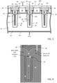
- FIG. 1 shows an embodiment of a cross-section of a split-gate trench power metal oxide semiconductor field effect transistor (MOSFET) device 10.
- MOSFET device 10 is an n-channel (nMOS) type device formed in and on a semiconductor substrate 12 (for example, silicon) doped with n-type dopant providing the drain region of the transistor 10.
- substrate 12 for example, silicon
- the substrate 12 has a front side 14 and a back side 16.
- a plurality of trenches 18 extend depthwise into the substrate 12 from the front side 14.
- the trenches 18 extend lengthwise parallel to each other in a direction perpendicular to the cross-section (i.e., into and out the page of the illustration), with adjacent trenches delimiting side edges of a mesa region 13 of the transistor forming a strip (this type of transistor device commonly referred to in the art as a strip-FET type transistor).
- a region 24 doped with a p-type dopant is buried in the mesa region 13 of the substrate 12 at a depth offset from (i.e., below) the front side 14 and positioned extending parallel to the front side 14 on opposite sides of each trench 18.
- the doped region 24 forms the body (channel) region of the transistor, with the trench 18 passing completely through the doped body region 24 and into the substrate 12 below the doped body region 24.
- a surface region 26 heavily doped with an n-type dopant is provided in the mesa region 13 at the front side 14 of the substrate 12 and positioned extending parallel to the front side 14 on opposite sides of each trench 18 and in contact with the top of the doped body region 24.
- the doped region 26 forms the source region of the transistor, with the trench 18 passing completely through the doped source region 26 and further extending, as noted above, completely through the doped body region 24 into the substrate 12 below the doped body region 24.
- each trench 18 is lined with a first insulating layer 20.
- the first insulating layer 20 may comprise an oxide layer (which, in an embodiment, is made up of both an oxide thermally grown from the exposed surfaces of the substrate 12 in each trench 18 and a deposited oxide).
- Each trench 18 is filled by a first polysilicon material 22, with the first insulating layer 20 insulating the first polysilicon material 22 from the substrate 12.
- an upper portion of the first insulating layer 20 (which would be adjacent to both the doped body region 24 and doped region 26, for example) is removed from an upper part of the trench 18 to expose a corresponding upper portion 22a of the first polysilicon material 22 and form an annular trench surrounding the upper portion 22a.
- the side walls (inner and outer) of the annular trench are lined with a second insulating layer 30a and third insulating layer 30b.
- the second and third insulating layers 30a, 30b may each comprise an oxide layer (which, in an embodiment, is thermally grown from the exposed surfaces of the substrate 12 in each annular trench and the exposed surfaces of the upper portion 22a of the first polysilicon material 22).
- the remaining open portion of each annular trench is then filled by a second polysilicon material 32, with the second insulating layer 30a insulating the polysilicon material 32 from the substrate 12 and the third insulating layer 30b insulating the polysilicon material 32 from the upper portion 22a.
- the first polysilicon material 22 in a lower part of the trench 18 forms a field plate electrode of the transistor 10.
- the second polysilicon material 32 in the upper part of the trench 18 forms the gate of the transistor 10 and extends on opposite sides of the upper portion 22a.
- the second insulating layer 30a forms the gate oxide layer.
- a stack 40 of layers is formed over each trench 18 and laterally extends on opposite sides of each trench 18 over at least a portion of the doped regions 26 for the source.
- Each stack 40 comprises a dielectric region formed by an undoped oxide (for example, tetraethyl orthosilicate (TEOS)) layer 44 and a glass (for example, borophosphosilicate glass (BPSG)) layer 46.
- TEOS tetraethyl orthosilicate
- BPSG borophosphosilicate glass
- a source metal contact 50 extends between adjacent stacks 40 to make electrical contact with each doped source region 26.
- Each source metal contact 50 extends depthwise into the substrate from the front side 14 to pass through the doped source region 26 and into the doped body region 24 (thus providing a body contact for the transistor 10 that is tied to the source).
- a source metal layer 52 extends over both the stacks 40 and the source metal contacts 50 to provide a metal connection to all the source metal contacts 50.
- the stack 40 insulates the source metal layer 52 and the source metal contacts 50 from the gate (polysilicon region 32).
- An electrical connection (not explicitly shown but schematically illustrated by dotted line 55) is provided to electrically connect the source metal layer 52 to the field plate (polysilicon region 22a).
- a drain metal layer 54 extends over the back side 16 of the substrate 12 to provide a metal connection to the drain.
- a gate metal layer (not explicitly shown as it is offset in a direction perpendicular to the cross-section) makes an electrical connection to the gate (polysilicon region 32) in each trench 18, this gate metal layer and electrical connection being schematically shown by dotted line 56.
- the transistor 10 could instead be a pMOS type transistor where the substrate 12 and doped source region 26 are both p-type doped and the body region 24 is n-type doped.
- a scanning electron micrograph (SEM) cross-sectional image of a single cell of the transistor 10 is shown in Figure 2 .
- SEM scanning electron micrograph
- the thickness of the gate oxide formed by the second insulating layer 30a between the gate (polysilicon region 32) and the substrate 12 in the upper part of the trench 18 (specifically in the annular trench region) must be thin.
- the thickness of the gate oxide is thinned from about 750-800 ⁇ to about 450-500 ⁇ , there is a corresponding reduction in the threshold voltage from about 3.5V to about 1.75V.
- the thermal oxidation process used to form the second insulating layer 30a affects not only the thickness of the gate oxide but also the isolation between the gate (polysilicon region 32) and the field plate electrode (polysilicon region 22) provided by third insulating layer 30b.
- the transistor 10 then experiences an unacceptable level of gate-to-source leakage current (IGSS) in response to the application of a gate voltage.
- IGSS gate-to-source leakage current
- a method comprises: forming a trench in a semiconductor substrate; lining the trench with a first insulation layer; filling the trench with a first conductive material insulated from the semiconductor substrate by said first insulating layer; recessing the first insulation layer to expose an upper portion of the first conductive material within an annual trench portion of said trench; filling the annular trench portion with a resist material; developing the resist material in the annular trench portion to expose an uppermost part of the upper portion of the first conductive material leaving residual resist on sidewalls of the trench which are spaced apart from said uppermost part and define a mask; etching using said mask to remove the upper portion of the first conductive material to a level of the recessed first insulation layer; removing the resist material to open an upper part of said trench; lining sidewalls of the upper part of said trench with a second insulating layer; lining a top surface of the first conductive material at a bottom of said upper part of said trench with a third insulating layer; and depositing a second conductive material in
- the first conductive material is made of polysilicon. In an embodiment, the second conductive material is made of polysilicon.
- the first insulating layer is a thermal oxide.
- the second insulating layer is a thermal oxide.
- the third insulating layer is a thermal oxide.
- the semiconductor substrate provides a drain region of a transistor, and the method further comprises:
- the first conductive material provides a field plate electrode of the transistor and the second conductive material provides a gate electrode of the transistor.
- the method further comprises:
- the third conductive material provides a source contact for the transistor.
- developing the resist material in the annular trench portion comprises exposing the resist material to light through a reticle having an opening larger than a dimension of the uppermost part of the upper portion of the first conductive material and smaller than a dimension of the trench.
- a method comprises: forming a trench in a semiconductor substrate; lining a lower part of the trench with a first insulation layer; filling the lower part of the trench with a first conductive material insulated from the semiconductor substrate by said first insulating layer; lining sidewalls of an upper part of said trench with a second insulating layer; lining a top surface of the first conductive material at a bottom of said upper part of said trench with a third insulating layer; and depositing a second conductive material in said upper part of said trench, said second conductive material insulated from the semiconductor substrate by said second insulating layer and insulated from the first conductive material by said third insulating layer.
- the first and second conductive materials are each made of polysilicon.
- the first, second and third insulating layers are each made of a thermal oxide.
- the semiconductor substrate provides a drain region of a transistor, and the method further comprises:
- the first conductive material provides a field plate electrode of the transistor and the second conductive material provides a gate electrode of the transistor.
- the method further comprises:
- the third conductive material provides a source contact for the transistor.
- the method further comprises using a resist material within the upper part of said trench as a mask for an etching operation to remove the first conductive material from the upper part of said trench.
- the method further comprises:
- the method further comprises removing the resist material within the upper part of said trench following the etching operation to remove the first conductive material from the upper part of said trench.
- developing the resist material comprises exposing the resist material to light through a reticle having an opening larger than a dimension of the uppermost part of the upper portion of the first conductive material and smaller than a dimension of the trench.
- exposing comprises using a light intensity which results in an underexposure of a portion of the resist material defined by the opening in the reticle.
- an integrated circuit comprises: a semiconductor substrate having a front surface and a back surface; a trench extending into the semiconductor substrate from the front surface, said trench including a lower part and an upper part; a first insulation layer lining the lower part of the trench; a first conductive material in the lower part of the trench and insulated from the semiconductor substrate by said first insulating layer; a second insulating layer lining sidewalls of the upper part of said trench; a third insulating layer lining a top surface of the first conductive material at a bottom of said upper part of said trench; and a second conductive material in said upper part of said trench, said second conductive material insulated from the semiconductor substrate by said second insulating layer and insulated from the first conductive material by said third insulating layer.
- the first and second conductive materials are each made of polysilicon.
- the first, second and third insulating layers are each made of a thermal oxide.
- the semiconductor substrate provides a drain region of a transistor
- the integrated circuit further comprises:
- the first conductive material provides a field plate electrode of the transistor and the second conductive material provides a gate electrode of the transistor.
- the integrated circuit further comprises:
- the third conductive material provides a source contact for the transistor.
- FIG. 3 shows a cross-section of an embodiment of a split-gate trench power metal oxide semiconductor field effect transistor (MOSFET) device 100.
- the MOSFET device 100 is an n-channel (nMOS) type device formed in and on a semiconductor substrate 12 (for example, silicon) doped with n-type dopant providing the drain region of the transistor 100.
- the substrate 12 has a front side 14 and a back side 16.
- a plurality of trenches 18 extend depthwise into the substrate 12 from the front side 14.
- the trenches 18 extend lengthwise parallel to each other in a direction perpendicular to the cross-section (i.e., into and out the page of the illustration), with adjacent trenches delimiting side edges of a mesa region 13 of the transistor forming a strip (this type of transistor device commonly referred to in the art as a strip-FET type transistor).
- Each trench 18 includes a lower part of the trench and an upper part of the trench.
- a region 24 doped with a p-type dopant is buried in the mesa region 13 of the substrate 12 at a depth offset from (i.e., below) the front side 14 and positioned extending parallel to the front side 14 on opposite sides of each trench 18.
- the doped region 24 forms the body (channel) region of the transistor, with the trench 18 passing completely through the doped body region 24 and into the substrate 12 below the doped body region 24.
- a surface region 26 heavily doped with an n-type dopant is provided in the mesa region 13 at the front side 14 of the substrate 12 and positioned extending parallel to the front side 14 on opposite sides of each trench 18 and in contact with the top of the doped body region 24.
- the doped region 26 forms the source region of the transistor, with the trench 18 passing completely through the doped source region 26 and further extending, as noted above, completely through the doped body region 24 into the substrate 12 below the doped body region 24.
- first insulating layer 20 may comprise an oxide layer (which, in an embodiment, is made up of an oxide thermally grown from the exposed surfaces of the substrate 12 in each trench 18 and a deposited oxide).
- the lower part of each trench 18 is filled by a first polysilicon material 22, with the first insulating layer 20 insulating the polysilicon material 22 from the substrate 12.
- an upper portion of the first insulating layer 20 and upper portion of the first polysilicon material 22 are removed (i.e., recessed) from the upper part of the trench 18.
- the second and third insulating layers 130, 132 may each comprise an oxide layer (which, in an embodiment, is thermally grown from the exposed surfaces of the substrate 12 in the upper part of the trench and the exposed upper end of the first polysilicon material 22).
- the remaining open space of the upper part of each trench 18 is then filled by a second polysilicon material 32, with the second insulating layer 130 insulating the polysilicon material 32 from the substrate 12 and the third insulating layer 132 insulating the polysilicon material 32 from the first polysilicon material 22.
- the first polysilicon material 22 forms a field plate electrode of the transistor 100.
- the second polysilicon material 32 forms the gate of the transistor 100.
- the second insulating layer 130 forms the gate oxide layer.
- a stack 40 of layers is formed over each trench 18 and laterally extends on opposite sides of each trench 18 over at least a portion of the doped regions 26 for the source.
- Each stack 40 comprises a dielectric region formed by an undoped oxide (for example, tetraethyl orthosilicate (TEOS)) layer 44 and a glass (for example, borophosphosilicate glass (BPSG)) layer 46.
- TEOS tetraethyl orthosilicate
- BPSG borophosphosilicate glass
- a source metal contact 50 extends between adjacent stacks 40 to make electrical contact with each doped source region 26.
- Each source metal contact 50 extends depthwise into the substrate from the front side 14 to pass through the doped source region 26 and into the doped body region 24 (thus providing a body contact for the transistor 100 that is tied to the source).
- a source metal layer 52 extends over both the stacks 40 and the source metal contacts 50 to provide a metal connection to all the source metal contacts 50.
- the stacks 40 insulate both the source metal layer 52 and the source metal contacts 50 from the gate (polysilicon region 32).
- An electrical connection (not explicitly shown) is provided to electrically connect the source metal layer 52 to the recessed polysilicon material 22 forming a field plate.
- a drain metal layer 54 extends over the back side 16 of the substrate 12 to provide a metal connection to the drain.
- a gate metal layer (not explicitly shown as it is offset in a direction perpendicular to the cross-section) makes an electrical connection to the gate (polysilicon region 32) in each trench 18, this gate metal layer and electrical connection being schematically shown by dotted line 56.
- the transistor 100 could instead be a pMOS type transistor where the substrate 12 and doped source region 26 are both p-type doped and the body region 24 is n-type doped.
- a scanning electron micrograph (SEM) cross-sectional image of a single cell of the transistor 100 is shown in Figure 4 .
- the power MOSFET 100 supports a lower threshold voltage because the thickness of the gate oxide formed by the second insulating layer 130 between the gate (polysilicon region 32) and the substrate 12 in the trench 18 can be controlled to be thin.
- the thickness of the gate oxide may be in the range of about 450-500 ⁇ .
- the position and thickness of the third insulating layer 132 can also be controlled to provide sufficient insulation between the gate (polysilicon region 32) and the field plate electrode (polysilicon region 22) to produce a strong poly-to-poly isolation in the region 70' necessary for achieving a desired level of gate-to-source leakage current (IGSS).
- IGSS gate-to-source leakage current
- a trench 18 is formed in a substrate 12.
- the sidewalls and bottom of the lower part and upper part of the trench 18 are lined with an insulating layer 20 that further extends on the front side 14 of the substrate 12.
- the lower and upper parts of the trench 18 are then filled with first polysilicon (conductive) material 22.
- a polishing operation for example, a chemical-mechanical polishing (CMP) is performed to remove the first polysilicon material 22 which is not located within the trench 18. The result is shown in Figure 5A .
- CMP chemical-mechanical polishing
- an etching operation E1 is performed to recess the first polysilicon material 22 below a level of the top surface 15 of the insulating layer 20.
- the result is shown in Figure 5B . More specifically, the etching performed at this step is a reactive ion etch (RIE).
- RIE reactive ion etch
- An etching operation E2 is then performed to recess the insulating layer 20 within the upper part of the trench 18 and expose an upper portion 22a of the first polysilicon material 22 within an annular trench portion of the upper part of the trench 18.
- the result is shown in Figure 5C . More specifically, the etching performed at this step is by a buffered oxide etch (BOE).
- BOE buffered oxide etch
- a resist layer 17 is then deposited to fill the area of trench 18 where the insulating layer 20 was recessed (i.e., the annular trench portion at the upper part of trench 18) and cover the front side 14 of the substrate 12. The result is shown in Figure 5D .
- a photolithography operation E3 is then performed to recess the resist layer 17 within the upper part of the trench 18 and expose an uppermost part 22b of the upper portion 22a of the first polysilicon material 22.
- the result is shown in Figure 5E .
- Figure 6 is a scanning electron micrograph image of a cross-section of the trench 18 at the step in the fabrication process shown by Figure 5E . More specifically, the photolithographic operation performed at this step includes a resist under-exposure technique followed by a subsequent resist development.
- the reticle 19 used for performing the photolithography operation E3 includes an opening 21 that is substantially aligned with the center of the first polysilicon material 22 (with some degree of misalignment tolerated due to the use of a under-exposure photolithography technique that is to be performed) and has width dimension d1 that is greater than the width d2 of the first polysilicon material 22 and less than the width d3 of the trench 18.
- width dimension d1 that is greater than the width d2 of the first polysilicon material 22 and less than the width d3 of the trench 18.
- the under-exposure photolithography (i.e., with reduced light intensity) process creates a self-aligned protection structure that ensures the annular trench portion and upper part of the substrate 12 is protected during subsequent fabrication process operations (such as, for example, the etching process E4 performed in the next step to create the recessed polysilicon 22). If this reduced under-exposure photolithography (with reduced light intensity) is not performed, and instead a standard exposure is made, the reticle opening 21 has to be designed exactly aligned to and with same dimensions as the polysilicon 22. This is very a difficult, if not impossible, process to industrialize with zero misalignment process margin.
- an etching operation E4 is then performed to further recess the first polysilicon material 22 (in particular, to remove the upper portion 22a of the first polysilicon material 22 within the upper part of the trench 18) to a level substantially equal to the level of an upper surface 20a of the previously recessed insulating layer 20 within the lower part of the trench 18.
- the result is shown in Figure 5F .
- the etching performed at this step is a reactive ion etch (RIE).
- a resist removal operation E5 is then performed to remove the mask formed by the developed resist 17 and open the upper part 18a of the trench 18.
- the result is shown in Figure 5G . More specifically, the resist removal performed at this step is made using a mixture of a sulfuric acid and hydrogen peroxide solution.
- a thermal oxidation is then performed to form the second insulating layer 130 on the sidewalls of the upper part 18a of the trench 18 and the third insulating layer 132 at the bottom of the upper part 18a on the top surface 22c of the remaining portion of the first polysilicon material 22 in the lower part of the trench 18.
- the result is shown in Figure 5H .
- the remaining open space of the upper part 18a of the trench 18 is filled with the second polysilicon (conductive) material 32.
- a plasma etching operation is performed to remove the second polysilicon material 32 which is not located within the upper part 18a of the trench 18. The result is shown in Figure 5I .
- the process then continues with standard fabrication techniques for completing construction of the transistor 100 (this including steps for implanting the source region 26 and body region 24).
- the stack 40 is deposited on the planarized surface of the substrate. Openings for the source-body contacts are then formed to extend through the stack 40 and into the substrate 12. The openings are then filled with the material for the source contact 50.
- the source layer 52 is then deposited over the stack 40 and source contact 50. At any suitable time in the process, the drain contact 54 may be deposited on the back side 16 of the substrate 12.
- Figure 3 The result of these standard fabrication techniques is shown in Figure 3 .
Landscapes
- Insulated Gate Type Field-Effect Transistor (AREA)
- Element Separation (AREA)
- Engineering & Computer Science (AREA)
- Manufacturing & Machinery (AREA)
- Electrodes Of Semiconductors (AREA)
Abstract
A semiconductor substrate (12) has a trench (18) extending from a front surface (14) and including a lower part and an upper part. A first insulation layer (20) lines the lower part of the trench, and a first conductive material (22) in the lower part is insulated from the semiconductor substrate by the first insulating layer to form a field plate electrode of a transistor. A second insulating layer (130) lines sidewalls of the upper part of said trench. A third insulating layer (132) lines a top surface of the first conductive material at a bottom of the upper part of the trench. A second conductive material (32) fills the upper part of the trench. The second conductive material forms a gate electrode of the transistor (100) that is insulated from the semiconductor substrate by the second insulating layer and further insulated from the first conductive material by the third insulating layer.
Description
- This application claims priority from
United States Provisional Application for Patent No. 63/065,198, filed August 13, 2020 - The present invention generally relates to metal oxide semiconductor field effect transistor (MOSFET) devices and, in particular, to a split-gate trench power MOSFET device.
- Reference is made to
Figure 1 which shows an embodiment of a cross-section of a split-gate trench power metal oxide semiconductor field effect transistor (MOSFET)device 10. In this example, theMOSFET device 10 is an n-channel (nMOS) type device formed in and on a semiconductor substrate 12 (for example, silicon) doped with n-type dopant providing the drain region of thetransistor 10. Thesubstrate 12 has afront side 14 and aback side 16. A plurality oftrenches 18 extend depthwise into thesubstrate 12 from thefront side 14. Thetrenches 18 extend lengthwise parallel to each other in a direction perpendicular to the cross-section (i.e., into and out the page of the illustration), with adjacent trenches delimiting side edges of amesa region 13 of the transistor forming a strip (this type of transistor device commonly referred to in the art as a strip-FET type transistor). - A
region 24 doped with a p-type dopant is buried in themesa region 13 of thesubstrate 12 at a depth offset from (i.e., below) thefront side 14 and positioned extending parallel to thefront side 14 on opposite sides of eachtrench 18. Thedoped region 24 forms the body (channel) region of the transistor, with thetrench 18 passing completely through thedoped body region 24 and into thesubstrate 12 below thedoped body region 24. Asurface region 26 heavily doped with an n-type dopant is provided in themesa region 13 at thefront side 14 of thesubstrate 12 and positioned extending parallel to thefront side 14 on opposite sides of eachtrench 18 and in contact with the top of thedoped body region 24. Thedoped region 26 forms the source region of the transistor, with thetrench 18 passing completely through thedoped source region 26 and further extending, as noted above, completely through thedoped body region 24 into thesubstrate 12 below thedoped body region 24. - The side walls and bottom of each
trench 18 are lined with a first insulatinglayer 20. For example, the firstinsulating layer 20 may comprise an oxide layer (which, in an embodiment, is made up of both an oxide thermally grown from the exposed surfaces of thesubstrate 12 in eachtrench 18 and a deposited oxide). Eachtrench 18 is filled by afirst polysilicon material 22, with the firstinsulating layer 20 insulating thefirst polysilicon material 22 from thesubstrate 12. During the process for fabricating thetransistor 10, an upper portion of the first insulating layer 20 (which would be adjacent to both thedoped body region 24 and dopedregion 26, for example) is removed from an upper part of thetrench 18 to expose a correspondingupper portion 22a of thefirst polysilicon material 22 and form an annular trench surrounding theupper portion 22a. The side walls (inner and outer) of the annular trench are lined with a secondinsulating layer 30a and third insulatinglayer 30b. For example, the second and thirdinsulating layers substrate 12 in each annular trench and the exposed surfaces of theupper portion 22a of the first polysilicon material 22). The remaining open portion of each annular trench is then filled by asecond polysilicon material 32, with the secondinsulating layer 30a insulating thepolysilicon material 32 from thesubstrate 12 and the thirdinsulating layer 30b insulating thepolysilicon material 32 from theupper portion 22a. Thefirst polysilicon material 22 in a lower part of thetrench 18 forms a field plate electrode of thetransistor 10. Thesecond polysilicon material 32 in the upper part of thetrench 18 forms the gate of thetransistor 10 and extends on opposite sides of theupper portion 22a. The secondinsulating layer 30a forms the gate oxide layer. - A
stack 40 of layers is formed over eachtrench 18 and laterally extends on opposite sides of eachtrench 18 over at least a portion of thedoped regions 26 for the source. Eachstack 40 comprises a dielectric region formed by an undoped oxide (for example, tetraethyl orthosilicate (TEOS))layer 44 and a glass (for example, borophosphosilicate glass (BPSG))layer 46. - A
source metal contact 50 extends betweenadjacent stacks 40 to make electrical contact with eachdoped source region 26. Eachsource metal contact 50 extends depthwise into the substrate from thefront side 14 to pass through thedoped source region 26 and into the doped body region 24 (thus providing a body contact for thetransistor 10 that is tied to the source). Asource metal layer 52 extends over both thestacks 40 and thesource metal contacts 50 to provide a metal connection to all thesource metal contacts 50. Thestack 40 insulates thesource metal layer 52 and thesource metal contacts 50 from the gate (polysilicon region 32). An electrical connection (not explicitly shown but schematically illustrated by dotted line 55) is provided to electrically connect thesource metal layer 52 to the field plate (polysilicon region 22a). Adrain metal layer 54 extends over theback side 16 of thesubstrate 12 to provide a metal connection to the drain. A gate metal layer (not explicitly shown as it is offset in a direction perpendicular to the cross-section) makes an electrical connection to the gate (polysilicon region 32) in eachtrench 18, this gate metal layer and electrical connection being schematically shown bydotted line 56. - The
transistor 10 could instead be a pMOS type transistor where thesubstrate 12 and dopedsource region 26 are both p-type doped and thebody region 24 is n-type doped. - A scanning electron micrograph (SEM) cross-sectional image of a single cell of the
transistor 10 is shown inFigure 2 . There is a desire to lower the threshold voltage of thepower MOSFET 10. To achieve this, the thickness of the gate oxide formed by the secondinsulating layer 30a between the gate (polysilicon region 32) and thesubstrate 12 in the upper part of the trench 18 (specifically in the annular trench region) must be thin. As an example, if the thickness of the gate oxide is thinned from about 750-800Å to about 450-500Å, there is a corresponding reduction in the threshold voltage from about 3.5V to about 1.75V. The thermal oxidation process used to form the secondinsulating layer 30a affects not only the thickness of the gate oxide but also the isolation between the gate (polysilicon region 32) and the field plate electrode (polysilicon region 22) provided by thirdinsulating layer 30b. In particular, there is a concern that in providing a thinner secondinsulating layer 30a in order to reduce the threshold voltage there would be a corresponding thinning of the third insulatinglayer 30b in theregion 70, with this thinned insulation layer resulting in a weak poly-to-poly isolation. Thetransistor 10 then experiences an unacceptable level of gate-to-source leakage current (IGSS) in response to the application of a gate voltage. - There is accordingly a need in the art for an improved split-gate trench MOSFET structure that supports a lower threshold voltage while continuing to satisfy gate-to-source leakage current requirements.
- In an embodiment, a method comprises: forming a trench in a semiconductor substrate; lining the trench with a first insulation layer; filling the trench with a first conductive material insulated from the semiconductor substrate by said first insulating layer; recessing the first insulation layer to expose an upper portion of the first conductive material within an annual trench portion of said trench; filling the annular trench portion with a resist material; developing the resist material in the annular trench portion to expose an uppermost part of the upper portion of the first conductive material leaving residual resist on sidewalls of the trench which are spaced apart from said uppermost part and define a mask; etching using said mask to remove the upper portion of the first conductive material to a level of the recessed first insulation layer; removing the resist material to open an upper part of said trench; lining sidewalls of the upper part of said trench with a second insulating layer; lining a top surface of the first conductive material at a bottom of said upper part of said trench with a third insulating layer; and depositing a second conductive material in said upper part of said trench, said second conductive material insulated from the semiconductor substrate by said second insulating layer and insulated from the first conductive material by said third insulating layer.
- In an embodiment, the first conductive material is made of polysilicon. In an embodiment, the second conductive material is made of polysilicon.
- In an embodiment, the first insulating layer is a thermal oxide. In an embodiment, the second insulating layer is a thermal oxide. In an embodiment, the third insulating layer is a thermal oxide.
- In an embodiment, the semiconductor substrate provides a drain region of a transistor, and the method further comprises:
- forming a doped buried region in the semiconductor substrate which provides a body region of the transistor; and
- forming a doped surface region in the semiconductor substrate over the doped buried region which provides a source region of the transistor.
- In an embodiment, the first conductive material provides a field plate electrode of the transistor and the second conductive material provides a gate electrode of the transistor.
- In an embodiment, the method further comprises:
- forming an opening extending through the doped surface region and into the doped buried region; and
- filling said opening with a third conductive material.
- In an embodiment, the third conductive material provides a source contact for the transistor.
- In an embodiment, developing the resist material in the annular trench portion comprises exposing the resist material to light through a reticle having an opening larger than a dimension of the uppermost part of the upper portion of the first conductive material and smaller than a dimension of the trench.
- In an embodiment, a method comprises: forming a trench in a semiconductor substrate; lining a lower part of the trench with a first insulation layer; filling the lower part of the trench with a first conductive material insulated from the semiconductor substrate by said first insulating layer; lining sidewalls of an upper part of said trench with a second insulating layer; lining a top surface of the first conductive material at a bottom of said upper part of said trench with a third insulating layer; and depositing a second conductive material in said upper part of said trench, said second conductive material insulated from the semiconductor substrate by said second insulating layer and insulated from the first conductive material by said third insulating layer.
- In an embodiment, the first and second conductive materials are each made of polysilicon.
- In an embodiment, the first, second and third insulating layers are each made of a thermal oxide.
- In an embodiment, the semiconductor substrate provides a drain region of a transistor, and the method further comprises:
- forming a doped buried region in the semiconductor substrate which provides a body region of the transistor; and
- forming a doped surface region in the semiconductor substrate over the doped buried region which provides a source region of the transistor.
- In an embodiment, the first conductive material provides a field plate electrode of the transistor and the second conductive material provides a gate electrode of the transistor.
- In an embodiment, the method further comprises:
- forming an opening extending through the doped surface region and into the doped buried region; and
- filling said opening with a third conductive material.
- In an embodiment, the third conductive material provides a source contact for the transistor.
- In an embodiment, the method further comprises using a resist material within the upper part of said trench as a mask for an etching operation to remove the first conductive material from the upper part of said trench.
- In an embodiment, the method further comprises:
- depositing the resist material in the upper part of said trench to surround an upper portion of said first conductive material; and
- developing the resist material to expose an uppermost part of the upper portion of the first conductive material leaving residual resist material on sidewalls of the upper part of said trench spaced apart from said uppermost part and define said mask.
- In an embodiment, the method further comprises removing the resist material within the upper part of said trench following the etching operation to remove the first conductive material from the upper part of said trench.
- In an embodiment, developing the resist material comprises exposing the resist material to light through a reticle having an opening larger than a dimension of the uppermost part of the upper portion of the first conductive material and smaller than a dimension of the trench.
- In an embodiment, exposing comprises using a light intensity which results in an underexposure of a portion of the resist material defined by the opening in the reticle.
- In an embodiment, an integrated circuit comprises: a semiconductor substrate having a front surface and a back surface; a trench extending into the semiconductor substrate from the front surface, said trench including a lower part and an upper part; a first insulation layer lining the lower part of the trench; a first conductive material in the lower part of the trench and insulated from the semiconductor substrate by said first insulating layer; a second insulating layer lining sidewalls of the upper part of said trench; a third insulating layer lining a top surface of the first conductive material at a bottom of said upper part of said trench; and a second conductive material in said upper part of said trench, said second conductive material insulated from the semiconductor substrate by said second insulating layer and insulated from the first conductive material by said third insulating layer.
- In an embodiment, the first and second conductive materials are each made of polysilicon.
- In an embodiment, the first, second and third insulating layers are each made of a thermal oxide.
- In an embodiment, the semiconductor substrate provides a drain region of a transistor, the integrated circuit further comprises:
- a doped buried region in the semiconductor substrate which provides a body region of the transistor; and
- a doped surface region in the semiconductor substrate over the doped buried region which provides a source region of the transistor.
- In an embodiment, the first conductive material provides a field plate electrode of the transistor and the second conductive material provides a gate electrode of the transistor.
- In an embodiment, the integrated circuit further comprises:
- opening extending through the doped surface region and into the doped buried region; and
- a third conductive material filling said opening.
- In an embodiment, the third conductive material provides a source contact for the transistor.
- For a better understanding of the embodiments, reference will now be made by way of example only to the accompanying figures in which:
-
Figure 1 is a cross-section of a power metal oxide semiconductor field effect transistor (MOSFET) device; -
Figure 2 is a scanning electron micrograph image of a cross-section of the power MOSFET device ofFigure 2 ; -
Figure 3 is a cross-section of a power MOSFET device; -
Figure 4 is a scanning electron micrograph image of a cross-section of the power MOSFET device ofFigure 3 ; -
Figures 5A-5I show process steps in the fabrication of the MOSFET device ofFigures 3-4 ; and -
Figure 6 is a scanning electron micrograph image of a cross-section of the trench at an intermediate step in the fabrication process shown inFigure 5E . - Reference is now made to
Figure 3 which shows a cross-section of an embodiment of a split-gate trench power metal oxide semiconductor field effect transistor (MOSFET)device 100. In this example, theMOSFET device 100 is an n-channel (nMOS) type device formed in and on a semiconductor substrate 12 (for example, silicon) doped with n-type dopant providing the drain region of thetransistor 100. Thesubstrate 12 has afront side 14 and aback side 16. A plurality oftrenches 18 extend depthwise into thesubstrate 12 from thefront side 14. Thetrenches 18 extend lengthwise parallel to each other in a direction perpendicular to the cross-section (i.e., into and out the page of the illustration), with adjacent trenches delimiting side edges of amesa region 13 of the transistor forming a strip (this type of transistor device commonly referred to in the art as a strip-FET type transistor). Eachtrench 18 includes a lower part of the trench and an upper part of the trench. - A
region 24 doped with a p-type dopant is buried in themesa region 13 of thesubstrate 12 at a depth offset from (i.e., below) thefront side 14 and positioned extending parallel to thefront side 14 on opposite sides of eachtrench 18. The dopedregion 24 forms the body (channel) region of the transistor, with thetrench 18 passing completely through the dopedbody region 24 and into thesubstrate 12 below the dopedbody region 24. Asurface region 26 heavily doped with an n-type dopant is provided in themesa region 13 at thefront side 14 of thesubstrate 12 and positioned extending parallel to thefront side 14 on opposite sides of eachtrench 18 and in contact with the top of the dopedbody region 24. The dopedregion 26 forms the source region of the transistor, with thetrench 18 passing completely through the dopedsource region 26 and further extending, as noted above, completely through the dopedbody region 24 into thesubstrate 12 below the dopedbody region 24. - The side walls and bottom of the lower part of each
trench 18 are lined with a first insulatinglayer 20. For example, the first insulatinglayer 20 may comprise an oxide layer (which, in an embodiment, is made up of an oxide thermally grown from the exposed surfaces of thesubstrate 12 in eachtrench 18 and a deposited oxide). The lower part of eachtrench 18 is filled by afirst polysilicon material 22, with the first insulatinglayer 20 insulating thepolysilicon material 22 from thesubstrate 12. During the process for fabricating thetransistor 100, an upper portion of the first insulatinglayer 20 and upper portion of the first polysilicon material 22 (which would be adjacent to both the dopedbody region 24 and dopedregion 26, for example) are removed (i.e., recessed) from the upper part of thetrench 18. This exposes a top surface of the recessedpolysilicon material 22 at the bottom of the upper part of thetrench 18. The side walls of the upper part of thetrench 18 are lined with a second insulatinglayer 130 and the top surface of the recessedpolysilicon material 22 is lined with a thirdinsulating layer 132. For example, the second and third insulatinglayers substrate 12 in the upper part of the trench and the exposed upper end of the first polysilicon material 22). The remaining open space of the upper part of eachtrench 18 is then filled by asecond polysilicon material 32, with the second insulatinglayer 130 insulating thepolysilicon material 32 from thesubstrate 12 and the third insulatinglayer 132 insulating thepolysilicon material 32 from thefirst polysilicon material 22. Thefirst polysilicon material 22 forms a field plate electrode of thetransistor 100. Thesecond polysilicon material 32 forms the gate of thetransistor 100. The secondinsulating layer 130 forms the gate oxide layer. - A
stack 40 of layers is formed over eachtrench 18 and laterally extends on opposite sides of eachtrench 18 over at least a portion of the dopedregions 26 for the source. Eachstack 40 comprises a dielectric region formed by an undoped oxide (for example, tetraethyl orthosilicate (TEOS))layer 44 and a glass (for example, borophosphosilicate glass (BPSG))layer 46. - A
source metal contact 50 extends betweenadjacent stacks 40 to make electrical contact with eachdoped source region 26. Eachsource metal contact 50 extends depthwise into the substrate from thefront side 14 to pass through the dopedsource region 26 and into the doped body region 24 (thus providing a body contact for thetransistor 100 that is tied to the source). Asource metal layer 52 extends over both thestacks 40 and thesource metal contacts 50 to provide a metal connection to all thesource metal contacts 50. Thestacks 40 insulate both thesource metal layer 52 and thesource metal contacts 50 from the gate (polysilicon region 32). An electrical connection (not explicitly shown) is provided to electrically connect thesource metal layer 52 to the recessedpolysilicon material 22 forming a field plate. Adrain metal layer 54 extends over theback side 16 of thesubstrate 12 to provide a metal connection to the drain. A gate metal layer (not explicitly shown as it is offset in a direction perpendicular to the cross-section) makes an electrical connection to the gate (polysilicon region 32) in eachtrench 18, this gate metal layer and electrical connection being schematically shown by dottedline 56. - The
transistor 100 could instead be a pMOS type transistor where thesubstrate 12 and dopedsource region 26 are both p-type doped and thebody region 24 is n-type doped. - A scanning electron micrograph (SEM) cross-sectional image of a single cell of the
transistor 100 is shown inFigure 4 . Thepower MOSFET 100 supports a lower threshold voltage because the thickness of the gate oxide formed by the second insulatinglayer 130 between the gate (polysilicon region 32) and thesubstrate 12 in thetrench 18 can be controlled to be thin. As an example, the thickness of the gate oxide may be in the range of about 450-500Å. The position and thickness of the third insulatinglayer 132 can also be controlled to provide sufficient insulation between the gate (polysilicon region 32) and the field plate electrode (polysilicon region 22) to produce a strong poly-to-poly isolation in the region 70' necessary for achieving a desired level of gate-to-source leakage current (IGSS). - Reference is now made to
Figures 5A-5I which show process steps in the fabrication of the MOSFET device ofFigure 3 . - A
trench 18 is formed in asubstrate 12. The sidewalls and bottom of the lower part and upper part of thetrench 18 are lined with an insulatinglayer 20 that further extends on thefront side 14 of thesubstrate 12. The lower and upper parts of thetrench 18 are then filled with first polysilicon (conductive)material 22. A polishing operation (for example, a chemical-mechanical polishing (CMP)) is performed to remove thefirst polysilicon material 22 which is not located within thetrench 18. The result is shown inFigure 5A . - Next, an etching operation E1 is performed to recess the
first polysilicon material 22 below a level of thetop surface 15 of the insulatinglayer 20. The result is shown inFigure 5B . More specifically, the etching performed at this step is a reactive ion etch (RIE). - An etching operation E2 is then performed to recess the insulating
layer 20 within the upper part of thetrench 18 and expose anupper portion 22a of thefirst polysilicon material 22 within an annular trench portion of the upper part of thetrench 18. The result is shown inFigure 5C . More specifically, the etching performed at this step is by a buffered oxide etch (BOE). - A resist
layer 17 is then deposited to fill the area oftrench 18 where the insulatinglayer 20 was recessed (i.e., the annular trench portion at the upper part of trench 18) and cover thefront side 14 of thesubstrate 12. The result is shown inFigure 5D . - A photolithography operation E3 is then performed to recess the resist
layer 17 within the upper part of thetrench 18 and expose anuppermost part 22b of theupper portion 22a of thefirst polysilicon material 22. The result is shown inFigure 5E .Figure 6 is a scanning electron micrograph image of a cross-section of thetrench 18 at the step in the fabrication process shown byFigure 5E . More specifically, the photolithographic operation performed at this step includes a resist under-exposure technique followed by a subsequent resist development. Thereticle 19 used for performing the photolithography operation E3 includes anopening 21 that is substantially aligned with the center of the first polysilicon material 22 (with some degree of misalignment tolerated due to the use of a under-exposure photolithography technique that is to be performed) and has width dimension d1 that is greater than the width d2 of thefirst polysilicon material 22 and less than the width d3 of thetrench 18. As a result,residual portions 17a of the resist 17 after the development in the photolithography operation E3 remain on sidewalls of the upper part of thetrench 18 spaced apart from theuppermost part 22b of theupper portion 22a of thefirst polysilicon material 22. - During the photolithography process to develop the resist 17 using
reticle 19 and itsopening 21, the under-exposure photolithography (i.e., with reduced light intensity) process creates a self-aligned protection structure that ensures the annular trench portion and upper part of thesubstrate 12 is protected during subsequent fabrication process operations (such as, for example, the etching process E4 performed in the next step to create the recessed polysilicon 22). If this reduced under-exposure photolithography (with reduced light intensity) is not performed, and instead a standard exposure is made, thereticle opening 21 has to be designed exactly aligned to and with same dimensions as thepolysilicon 22. This is very a difficult, if not impossible, process to industrialize with zero misalignment process margin. - Using the mask formed by the developed resist 17, an etching operation E4 is then performed to further recess the first polysilicon material 22 (in particular, to remove the
upper portion 22a of thefirst polysilicon material 22 within the upper part of the trench 18) to a level substantially equal to the level of anupper surface 20a of the previously recessed insulatinglayer 20 within the lower part of thetrench 18. The result is shown inFigure 5F . More specifically, the etching performed at this step is a reactive ion etch (RIE). - A resist removal operation E5 is then performed to remove the mask formed by the developed resist 17 and open the
upper part 18a of thetrench 18. The result is shown inFigure 5G . More specifically, the resist removal performed at this step is made using a mixture of a sulfuric acid and hydrogen peroxide solution. - A thermal oxidation is then performed to form the second insulating
layer 130 on the sidewalls of theupper part 18a of thetrench 18 and the third insulatinglayer 132 at the bottom of theupper part 18a on thetop surface 22c of the remaining portion of thefirst polysilicon material 22 in the lower part of thetrench 18. The result is shown inFigure 5H . - Next, the remaining open space of the
upper part 18a of thetrench 18 is filled with the second polysilicon (conductive)material 32. A plasma etching operation is performed to remove thesecond polysilicon material 32 which is not located within theupper part 18a of thetrench 18. The result is shown inFigure 5I . - The process then continues with standard fabrication techniques for completing construction of the transistor 100 (this including steps for implanting the
source region 26 and body region 24). Thestack 40 is deposited on the planarized surface of the substrate. Openings for the source-body contacts are then formed to extend through thestack 40 and into thesubstrate 12. The openings are then filled with the material for thesource contact 50. Thesource layer 52 is then deposited over thestack 40 andsource contact 50. At any suitable time in the process, thedrain contact 54 may be deposited on theback side 16 of thesubstrate 12. The result of these standard fabrication techniques is shown inFigure 3 . - While the invention has been illustrated and described in detail in the drawings and foregoing description, such illustration and description are considered illustrative or exemplary and not restrictive; the invention is not limited to the disclosed embodiments. Other variations to the disclosed embodiments can be understood and effected by those skilled in the art in practicing the claimed invention, from a study of the drawings, the disclosure, and the appended claims.
Claims (15)
- A method, comprising:forming a trench (18) in a semiconductor substrate (12);lining the trench with a first insulation layer (20);filling the trench with a first conductive material (22) insulated from the semiconductor substrate (12) by said first insulating layer;recessing the first insulation layer (20) to expose an upper portion (22a) of the first conductive material (22) within an annual trench portion of said trench;filling the annular trench portion with a resist material (17);developing the resist material (17) in the annular trench portion to expose an uppermost part (22b) of the upper portion (22a) of the first conductive material (22) leaving residual resist material (17a) on sidewalls of the trench which are spaced apart from said uppermost part and define a mask;etching using said mask to remove the upper portion (22a) of the first conductive material (22) to a level (23) of the recessed first insulation layer (20);removing the residual resist material (17a) to open an upper part (18a) of said trench;lining sidewalls of the upper part of said trench with a second insulating layer (130);lining a top surface (22c) of the first conductive material (22) at a bottom of said upper part of said trench with a third insulating layer (132); anddepositing a second conductive material (32) in said upper part of said trench, said second conductive material insulated from the semiconductor substrate (12) by said second insulating layer and insulated from the first conductive material (22) by said third insulating layer.
- A method, comprising:forming a trench (18) in a semiconductor substrate (12);lining a lower part of the trench with a first insulation layer (20);filling the lower part of the trench with a first conductive material (22) insulated from the semiconductor substrate (12) by said first insulating layer;lining sidewalls of an upper part (18a) of said trench (18) with a second insulating layer (130);lining a top surface (22c) of the first conductive material (22) at a bottom of said upper part of said trench with a third insulating layer (132); anddepositing a second conductive material (32) in said upper part of said trench, said second conductive material insulated from the semiconductor substrate (12) by said second insulating layer and insulated from the first conductive material (22) by said third insulating layer.
- The method of claim 2, further comprising using a resist material (17) within the upper part (18a) of said trench as a mask for an etching operation to remove the first conductive material (22) from the upper part of said trench.
- The method of claim 3, further comprising:depositing the resist material (17) in the upper part (18a) of said trench to surround an upper portion (22a) of said first conductive material; anddeveloping the resist material (17) to expose an uppermost part (22b) of the upper portion (22a) of the first conductive material (22) leaving residual resist material (17a) on sidewalls of the upper part (18a) of said trench spaced apart from said uppermost part and define said mask.
- The method of claim 4, further comprising removing the resist material (17) within the upper part (18a) of said trench following the etching operation to remove the first conductive material (22) from the upper part of said trench.
- The method of claim 1, 4 or 5, wherein developing the resist material (17) comprises exposing the resist material to light through a reticle (19) having an opening (21) larger than a dimension (d2) of the uppermost part (22b) of the upper portion (22a) of the first conductive material (22) and smaller than a dimension (d3) of the trench (18).
- The method of claim 6, wherein exposing comprises using a light intensity which results in an underexposure of a portion of the resist material (17) defined by the opening (21) in the reticle (19).
- The method of any of claims 1 to 7, wherein the semiconductor substrate (12) provides a drain region of a transistor (100), further comprising:forming a doped buried region (24) in the semiconductor substrate which provides a body region of the transistor; andforming a doped surface region (26) in the semiconductor substrate over the doped buried region which provides a source region of the transistor.
- The method of claim 8, further comprising:forming an opening extending through the doped surface region (24) and into the doped buried region (26); andfilling said opening with a third conductive material, the third conductive material providing for example a source contact (50) for the transistor.
- An integrated circuit, comprising:a semiconductor substrate (12) having a front surface (14) and a back surface (16);a trench (18) extending into the semiconductor substrate from the front surface, said trench including a lower part and an upper part;a first insulation layer (20) lining the lower part of the trench;a first conductive material (22) in the lower part of the trench and insulated from the semiconductor substrate by said first insulating layer;a second insulating layer (130) lining sidewalls of the upper part of said trench;a third insulating layer (132) lining a top surface of the first conductive material at a bottom of said upper part of said trench; anda second conductive material (32) in said upper part of said trench, said second conductive material insulated from the semiconductor substrate by said second insulating layer and insulated from the first conductive material by said third insulating layer.
- The integrated circuit of claim 10 or the method of any of claims 1 to 9, wherein the first conductive material (22) and/or second conductive material (32) is made of polysilicon.
- The integrated circuit of claim 10 or 11 or the method of any of claims 1 to 9 and 11, wherein the first insulating layer (20), and/or the second insulating layer (130), and/or the third insulating layer (132) is made of a thermal oxide.
- The integrated circuit of any of claims 9 to 12, wherein the semiconductor substrate (12) provides a drain region of a transistor (100), further comprising:a doped buried region (24) in the semiconductor substrate which provides a body region of the transistor; anda doped surface region (26) in the semiconductor substrate over the doped buried region which provides a source region of the transistor.
- The integrated circuit of claim 13 or the method of claim 8, wherein the first conductive material (22) provides a field plate electrode of the transistor (100) and the second conductive material (32) provides a gate electrode of the transistor (100).
- The integrated circuit of claim 13 or 14, further comprising:an opening extending through the doped surface region (24) and into the doped buried region (26); anda third conductive material filling said opening, the third conductive material providing for example a source contact (50) for the transistor.
Applications Claiming Priority (2)
| Application Number | Priority Date | Filing Date | Title |
|---|---|---|---|
| US202063065198P | 2020-08-13 | 2020-08-13 | |
| US17/373,198 US11848378B2 (en) | 2020-08-13 | 2021-07-12 | Split-gate trench power MOSFET with self-aligned poly-to-poly isolation |
Publications (1)
| Publication Number | Publication Date |
|---|---|
| EP3955311A1 true EP3955311A1 (en) | 2022-02-16 |
Family
ID=77179947
Family Applications (1)
| Application Number | Title | Priority Date | Filing Date |
|---|---|---|---|
| EP21189249.2A Pending EP3955311A1 (en) | 2020-08-13 | 2021-08-03 | Split-gate trench power mosfet with self-aligned poly-to-poly isolation |
Country Status (3)
| Country | Link |
|---|---|
| US (1) | US11848378B2 (en) |
| EP (1) | EP3955311A1 (en) |
| CN (2) | CN114078710B (en) |
Families Citing this family (2)
| Publication number | Priority date | Publication date | Assignee | Title |
|---|---|---|---|---|
| US11848378B2 (en) * | 2020-08-13 | 2023-12-19 | Stmicroelectronics Pte Ltd | Split-gate trench power MOSFET with self-aligned poly-to-poly isolation |
| US12495577B2 (en) | 2022-08-17 | 2025-12-09 | Analog Devices, Inc. | Self-aligned silicide gate for discrete shielded-gate trench power MOSFET |
Citations (5)
| Publication number | Priority date | Publication date | Assignee | Title |
|---|---|---|---|---|
| US20070155104A1 (en) * | 2006-01-05 | 2007-07-05 | Marchant Bruce D | Power device utilizing chemical mechanical planarization |
| WO2008036603A1 (en) * | 2006-09-20 | 2008-03-27 | Fairchild Semiconductor Corporation | Trench gate fet with self-aligned features |
| US20100044785A1 (en) * | 2008-01-15 | 2010-02-25 | Murphy James J | High aspect ratio trench structures with void-free fill material |
| US20110133258A1 (en) * | 2009-08-14 | 2011-06-09 | Alpha And Omega Semiconductor Incorporated | Shielded gate trench mosfet with increased source-metal contact |
| US20160300917A1 (en) * | 2015-04-08 | 2016-10-13 | Alpha And Omega Semiconductor Incorporated | Self-aligned contact for trench power mosfet |
Family Cites Families (26)
| Publication number | Priority date | Publication date | Assignee | Title |
|---|---|---|---|---|
| US6259131B1 (en) | 1998-05-27 | 2001-07-10 | Taiwan Semiconductor Manufacturing Company | Poly tip and self aligned source for split-gate flash cell |
| US6309928B1 (en) | 1998-12-10 | 2001-10-30 | Taiwan Semiconductor Manufacturing Company | Split-gate flash cell |
| US6313500B1 (en) | 1999-01-12 | 2001-11-06 | Agere Systems Guardian Corp. | Split gate memory cell |
| US6358796B1 (en) | 1999-04-15 | 2002-03-19 | Taiwan Semiconductor Manufacturing Company | Method to fabricate a non-smiling effect structure in split-gate flash with self-aligned isolation |
| US6204126B1 (en) | 2000-02-18 | 2001-03-20 | Taiwan Semiconductor Manufacturing Company | Method to fabricate a new structure with multi-self-aligned for split-gate flash |
| US6420232B1 (en) | 2000-11-14 | 2002-07-16 | Silicon-Based Technology Corp. | Methods of fabricating a scalable split-gate flash memory device having embedded triple-sides erase cathodes |
| US6573142B1 (en) | 2002-02-26 | 2003-06-03 | Taiwan Semiconductor Manufacturing Company | Method to fabricate self-aligned source and drain in split gate flash |
| US7091573B2 (en) * | 2002-03-19 | 2006-08-15 | Infineon Technologies Ag | Power transistor |
| US6525369B1 (en) | 2002-05-13 | 2003-02-25 | Ching-Yuan Wu | Self-aligned split-gate flash memory cell and its contactless flash memory arrays |
| WO2006127914A2 (en) * | 2005-05-26 | 2006-11-30 | Fairchild Semiconductor Corporation | Trench-gate field effect transistors and methods of forming the same |
| US7385248B2 (en) * | 2005-08-09 | 2008-06-10 | Fairchild Semiconductor Corporation | Shielded gate field effect transistor with improved inter-poly dielectric |
| US20080150013A1 (en) * | 2006-12-22 | 2008-06-26 | Alpha & Omega Semiconductor, Ltd | Split gate formation with high density plasma (HDP) oxide layer as inter-polysilicon insulation layer |
| US8497549B2 (en) * | 2007-08-21 | 2013-07-30 | Fairchild Semiconductor Corporation | Method and structure for shielded gate trench FET |
| CN102007584B (en) | 2008-02-14 | 2013-01-16 | 马克斯半导体股份有限公司 | Semiconductor device structures and related processes |
| US8680614B2 (en) | 2012-06-12 | 2014-03-25 | Monolithic Power Systems, Inc. | Split trench-gate MOSFET with integrated Schottky diode |
| CN105355548B (en) * | 2015-10-27 | 2018-08-21 | 上海华虹宏力半导体制造有限公司 | The manufacturing method of trench gate mosfet with shield grid |
| CN205789991U (en) * | 2016-06-23 | 2016-12-07 | 无锡新洁能股份有限公司 | Groove type power MOS FET device |
| JP6866792B2 (en) * | 2017-07-21 | 2021-04-28 | 株式会社デンソー | Semiconductor devices and their manufacturing methods |
| JP2020004883A (en) * | 2018-06-29 | 2020-01-09 | 京セラ株式会社 | Semiconductor device, electric device, and method of manufacturing semiconductor device |
| US11127852B2 (en) * | 2018-12-27 | 2021-09-21 | Texas Instruments Incorporated | Vertical trench gate MOSFET with deep well region for junction termination |
| JP2020150185A (en) * | 2019-03-14 | 2020-09-17 | 株式会社東芝 | Semiconductor device |
| CN112864018B (en) * | 2019-11-28 | 2022-07-19 | 华润微电子(重庆)有限公司 | Groove type field effect transistor structure and preparation method thereof |
| EP3859788A1 (en) * | 2020-01-29 | 2021-08-04 | Infineon Technologies Austria AG | Transistor device and method of forming a field plate in an elongate active trench of a transistor device |
| CN115053352A (en) * | 2020-02-07 | 2022-09-13 | 罗姆股份有限公司 | Semiconductor device with a plurality of semiconductor chips |
| US11848378B2 (en) * | 2020-08-13 | 2023-12-19 | Stmicroelectronics Pte Ltd | Split-gate trench power MOSFET with self-aligned poly-to-poly isolation |
| CN115832019A (en) * | 2021-09-17 | 2023-03-21 | 德州仪器公司 | Field plate arrangement for trench gate field effect transistor |
-
2021
- 2021-07-12 US US17/373,198 patent/US11848378B2/en active Active
- 2021-08-03 EP EP21189249.2A patent/EP3955311A1/en active Pending
- 2021-08-12 CN CN202110924322.5A patent/CN114078710B/en active Active
- 2021-08-12 CN CN202121890323.4U patent/CN216671642U/en active Active
Patent Citations (5)
| Publication number | Priority date | Publication date | Assignee | Title |
|---|---|---|---|---|
| US20070155104A1 (en) * | 2006-01-05 | 2007-07-05 | Marchant Bruce D | Power device utilizing chemical mechanical planarization |
| WO2008036603A1 (en) * | 2006-09-20 | 2008-03-27 | Fairchild Semiconductor Corporation | Trench gate fet with self-aligned features |
| US20100044785A1 (en) * | 2008-01-15 | 2010-02-25 | Murphy James J | High aspect ratio trench structures with void-free fill material |
| US20110133258A1 (en) * | 2009-08-14 | 2011-06-09 | Alpha And Omega Semiconductor Incorporated | Shielded gate trench mosfet with increased source-metal contact |
| US20160300917A1 (en) * | 2015-04-08 | 2016-10-13 | Alpha And Omega Semiconductor Incorporated | Self-aligned contact for trench power mosfet |
Also Published As
| Publication number | Publication date |
|---|---|
| CN114078710A (en) | 2022-02-22 |
| CN114078710B (en) | 2025-11-11 |
| US11848378B2 (en) | 2023-12-19 |
| US20220052194A1 (en) | 2022-02-17 |
| CN216671642U (en) | 2022-06-03 |
Similar Documents
| Publication | Publication Date | Title |
|---|---|---|
| US6737308B2 (en) | Semiconductor device having LDD-type source/drain regions and fabrication method thereof | |
| JP4829473B2 (en) | Insulated gate semiconductor device and manufacturing method thereof | |
| US6548859B2 (en) | MOS semiconductor device and method of manufacturing the same | |
| US7494883B2 (en) | Semiconductor device having a trench isolation and method of fabricating the same | |
| US20090263948A1 (en) | Metal oxide semiconductor field-effect transistor (mosfet) and method of fabricating the same | |
| CN107464784B (en) | Manufacturing method of semiconductor device | |
| US7166514B2 (en) | Semiconductor device and method of manufacturing the same | |
| US20070023832A1 (en) | Semiconductor device and method of fabricating the same | |
| JP5234886B2 (en) | Manufacturing method of semiconductor device | |
| US11848378B2 (en) | Split-gate trench power MOSFET with self-aligned poly-to-poly isolation | |
| KR20090017842A (en) | Method for forming nonvolatile memory device having floating gate and related device | |
| CN107301971A (en) | Semiconductor devices and its manufacture method | |
| US7494895B2 (en) | Method of fabricating a three-dimensional MOSFET employing a hard mask spacer | |
| CN118431290A (en) | Trench type power device, preparation method, power module, conversion circuit and vehicle | |
| US20080135973A1 (en) | Semiconductor device comprising high-withstand voltage mosfet and its manufacturing method | |
| JP2018046234A (en) | Manufacturing method of semiconductor device | |
| US7772634B2 (en) | Semiconductor device and manufacturing method thereof | |
| KR100680429B1 (en) | Manufacturing Method of Semiconductor Device | |
| KR100281272B1 (en) | Method for forming element isolation insulating film of semiconductor element | |
| KR100636919B1 (en) | Manufacturing Method of Semiconductor Device | |
| US20170221711A1 (en) | Method of high voltage device fabrication | |
| EP4425567A1 (en) | Split-gate trench power mosfet with thick poly-to-poly isolation | |
| US20240234566A1 (en) | Method of forming high voltage transistor and structure resulting therefrom | |
| KR100586553B1 (en) | Gate of semiconductor device and forming method thereof | |
| KR100835471B1 (en) | Manufacturing method of semiconductor device |
Legal Events
| Date | Code | Title | Description |
|---|---|---|---|
| PUAI | Public reference made under article 153(3) epc to a published international application that has entered the european phase |
Free format text: ORIGINAL CODE: 0009012 |
|
| STAA | Information on the status of an ep patent application or granted ep patent |
Free format text: STATUS: REQUEST FOR EXAMINATION WAS MADE |
|
| 17P | Request for examination filed |
Effective date: 20210803 |
|
| AK | Designated contracting states |
Kind code of ref document: A1 Designated state(s): AL AT BE BG CH CY CZ DE DK EE ES FI FR GB GR HR HU IE IS IT LI LT LU LV MC MK MT NL NO PL PT RO RS SE SI SK SM TR |
|
| STAA | Information on the status of an ep patent application or granted ep patent |
Free format text: STATUS: EXAMINATION IS IN PROGRESS |
|
| 17Q | First examination report despatched |
Effective date: 20230922 |