CN107464784B - Method for manufacturing semiconductor device - Google Patents
Method for manufacturing semiconductor device Download PDFInfo
- Publication number
- CN107464784B CN107464784B CN201710356005.1A CN201710356005A CN107464784B CN 107464784 B CN107464784 B CN 107464784B CN 201710356005 A CN201710356005 A CN 201710356005A CN 107464784 B CN107464784 B CN 107464784B
- Authority
- CN
- China
- Prior art keywords
- region
- insulating film
- etching
- layer
- semiconductor
- Prior art date
- Legal status (The legal status is an assumption and is not a legal conclusion. Google has not performed a legal analysis and makes no representation as to the accuracy of the status listed.)
- Active
Links
- 239000004065 semiconductor Substances 0.000 title claims abstract description 569
- 238000000034 method Methods 0.000 title claims abstract description 111
- 238000004519 manufacturing process Methods 0.000 title claims abstract description 96
- 238000005530 etching Methods 0.000 claims abstract description 483
- 239000000758 substrate Substances 0.000 claims abstract description 233
- 238000002955 isolation Methods 0.000 claims abstract description 158
- 239000012535 impurity Substances 0.000 claims abstract description 70
- KRHYYFGTRYWZRS-UHFFFAOYSA-N Fluorane Chemical compound F KRHYYFGTRYWZRS-UHFFFAOYSA-N 0.000 claims description 44
- 229910052710 silicon Inorganic materials 0.000 claims description 41
- 239000010703 silicon Substances 0.000 claims description 41
- VYPSYNLAJGMNEJ-UHFFFAOYSA-N Silicium dioxide Chemical compound O=[Si]=O VYPSYNLAJGMNEJ-UHFFFAOYSA-N 0.000 claims description 30
- 229910052814 silicon oxide Inorganic materials 0.000 claims description 30
- 238000001039 wet etching Methods 0.000 claims description 29
- 239000000463 material Substances 0.000 claims description 24
- 229910052581 Si3N4 Inorganic materials 0.000 claims description 10
- HQVNEWCFYHHQES-UHFFFAOYSA-N silicon nitride Chemical compound N12[Si]34N5[Si]62N3[Si]51N64 HQVNEWCFYHHQES-UHFFFAOYSA-N 0.000 claims description 10
- 229910021421 monocrystalline silicon Inorganic materials 0.000 claims description 9
- 230000000149 penetrating effect Effects 0.000 claims description 8
- 210000000746 body region Anatomy 0.000 abstract description 164
- 238000005468 ion implantation Methods 0.000 abstract description 81
- 239000007788 liquid Substances 0.000 abstract description 45
- 239000010410 layer Substances 0.000 description 475
- 239000010408 film Substances 0.000 description 466
- 229920002120 photoresistant polymer Polymers 0.000 description 64
- 230000008569 process Effects 0.000 description 53
- XUIMIQQOPSSXEZ-UHFFFAOYSA-N Silicon Chemical compound [Si] XUIMIQQOPSSXEZ-UHFFFAOYSA-N 0.000 description 39
- 150000002500 ions Chemical class 0.000 description 33
- 125000006850 spacer group Chemical group 0.000 description 25
- 229910052751 metal Inorganic materials 0.000 description 16
- 239000002184 metal Substances 0.000 description 16
- 230000015572 biosynthetic process Effects 0.000 description 14
- 239000004020 conductor Substances 0.000 description 14
- 229910021332 silicide Inorganic materials 0.000 description 12
- FVBUAEGBCNSCDD-UHFFFAOYSA-N silicide(4-) Chemical compound [Si-4] FVBUAEGBCNSCDD-UHFFFAOYSA-N 0.000 description 12
- 230000004888 barrier function Effects 0.000 description 10
- 238000000206 photolithography Methods 0.000 description 9
- 238000005498 polishing Methods 0.000 description 9
- 230000000903 blocking effect Effects 0.000 description 8
- RYGMFSIKBFXOCR-UHFFFAOYSA-N Copper Chemical compound [Cu] RYGMFSIKBFXOCR-UHFFFAOYSA-N 0.000 description 6
- 229910052802 copper Inorganic materials 0.000 description 6
- 239000010949 copper Substances 0.000 description 6
- 239000002344 surface layer Substances 0.000 description 6
- OAICVXFJPJFONN-UHFFFAOYSA-N Phosphorus Chemical compound [P] OAICVXFJPJFONN-UHFFFAOYSA-N 0.000 description 5
- 229910052785 arsenic Inorganic materials 0.000 description 5
- RQNWIZPPADIBDY-UHFFFAOYSA-N arsenic atom Chemical compound [As] RQNWIZPPADIBDY-UHFFFAOYSA-N 0.000 description 5
- 238000002513 implantation Methods 0.000 description 5
- 229910052698 phosphorus Inorganic materials 0.000 description 5
- 239000011574 phosphorus Substances 0.000 description 5
- NBIIXXVUZAFLBC-UHFFFAOYSA-N Phosphoric acid Chemical compound OP(O)(O)=O NBIIXXVUZAFLBC-UHFFFAOYSA-N 0.000 description 4
- 238000005229 chemical vapour deposition Methods 0.000 description 4
- 239000000470 constituent Substances 0.000 description 4
- 230000000694 effects Effects 0.000 description 4
- 230000012447 hatching Effects 0.000 description 4
- 238000007747 plating Methods 0.000 description 4
- 230000004913 activation Effects 0.000 description 3
- QVGXLLKOCUKJST-UHFFFAOYSA-N atomic oxygen Chemical compound [O] QVGXLLKOCUKJST-UHFFFAOYSA-N 0.000 description 3
- 230000007547 defect Effects 0.000 description 3
- 238000001312 dry etching Methods 0.000 description 3
- 238000010438 heat treatment Methods 0.000 description 3
- 239000012212 insulator Substances 0.000 description 3
- 230000003647 oxidation Effects 0.000 description 3
- 238000007254 oxidation reaction Methods 0.000 description 3
- 229910052760 oxygen Inorganic materials 0.000 description 3
- 239000001301 oxygen Substances 0.000 description 3
- 238000000059 patterning Methods 0.000 description 3
- WFKWXMTUELFFGS-UHFFFAOYSA-N tungsten Chemical compound [W] WFKWXMTUELFFGS-UHFFFAOYSA-N 0.000 description 3
- 229910052721 tungsten Inorganic materials 0.000 description 3
- 239000010937 tungsten Substances 0.000 description 3
- QGZKDVFQNNGYKY-UHFFFAOYSA-N Ammonia Chemical compound N QGZKDVFQNNGYKY-UHFFFAOYSA-N 0.000 description 2
- ZOXJGFHDIHLPTG-UHFFFAOYSA-N Boron Chemical compound [B] ZOXJGFHDIHLPTG-UHFFFAOYSA-N 0.000 description 2
- MHAJPDPJQMAIIY-UHFFFAOYSA-N Hydrogen peroxide Chemical compound OO MHAJPDPJQMAIIY-UHFFFAOYSA-N 0.000 description 2
- 229910000147 aluminium phosphate Inorganic materials 0.000 description 2
- 238000000137 annealing Methods 0.000 description 2
- 238000004380 ashing Methods 0.000 description 2
- 229910052796 boron Inorganic materials 0.000 description 2
- 230000000994 depressogenic effect Effects 0.000 description 2
- 238000009792 diffusion process Methods 0.000 description 2
- 239000005001 laminate film Substances 0.000 description 2
- 239000000203 mixture Substances 0.000 description 2
- 238000012986 modification Methods 0.000 description 2
- 230000004048 modification Effects 0.000 description 2
- 238000007517 polishing process Methods 0.000 description 2
- 229910021420 polycrystalline silicon Inorganic materials 0.000 description 2
- 229920005591 polysilicon Polymers 0.000 description 2
- 239000000126 substance Substances 0.000 description 2
- 239000010409 thin film Substances 0.000 description 2
- BGTBFNDXYDYBEY-FNORWQNLSA-N 4-(2,6,6-Trimethylcyclohex-1-enyl)but-2-en-4-one Chemical compound C\C=C\C(=O)C1=C(C)CCCC1(C)C BGTBFNDXYDYBEY-FNORWQNLSA-N 0.000 description 1
- VHUUQVKOLVNVRT-UHFFFAOYSA-N Ammonium hydroxide Chemical compound [NH4+].[OH-] VHUUQVKOLVNVRT-UHFFFAOYSA-N 0.000 description 1
- 229910001260 Pt alloy Inorganic materials 0.000 description 1
- 241001255830 Thema Species 0.000 description 1
- 230000002411 adverse Effects 0.000 description 1
- 229910052782 aluminium Inorganic materials 0.000 description 1
- XAGFODPZIPBFFR-UHFFFAOYSA-N aluminium Chemical compound [Al] XAGFODPZIPBFFR-UHFFFAOYSA-N 0.000 description 1
- 229910021529 ammonia Inorganic materials 0.000 description 1
- 230000015556 catabolic process Effects 0.000 description 1
- 238000000576 coating method Methods 0.000 description 1
- 229910017052 cobalt Inorganic materials 0.000 description 1
- 239000010941 cobalt Substances 0.000 description 1
- GUTLYIVDDKVIGB-UHFFFAOYSA-N cobalt atom Chemical compound [Co] GUTLYIVDDKVIGB-UHFFFAOYSA-N 0.000 description 1
- 238000010586 diagram Methods 0.000 description 1
- 230000009977 dual effect Effects 0.000 description 1
- 238000005516 engineering process Methods 0.000 description 1
- 230000005669 field effect Effects 0.000 description 1
- 238000011049 filling Methods 0.000 description 1
- CUPFNGOKRMWUOO-UHFFFAOYSA-N hydron;difluoride Chemical compound F.F CUPFNGOKRMWUOO-UHFFFAOYSA-N 0.000 description 1
- 239000007943 implant Substances 0.000 description 1
- 230000006872 improvement Effects 0.000 description 1
- 239000011229 interlayer Substances 0.000 description 1
- PCLURTMBFDTLSK-UHFFFAOYSA-N nickel platinum Chemical compound [Ni].[Pt] PCLURTMBFDTLSK-UHFFFAOYSA-N 0.000 description 1
- 230000001590 oxidative effect Effects 0.000 description 1
- 230000036961 partial effect Effects 0.000 description 1
- 230000002265 prevention Effects 0.000 description 1
- 238000000926 separation method Methods 0.000 description 1
- 230000036962 time dependent Effects 0.000 description 1
Images


Classifications
-
- H—ELECTRICITY
- H01—ELECTRIC ELEMENTS
- H01L—SEMICONDUCTOR DEVICES NOT COVERED BY CLASS H10
- H01L27/00—Devices consisting of a plurality of semiconductor or other solid-state components formed in or on a common substrate
- H01L27/02—Devices consisting of a plurality of semiconductor or other solid-state components formed in or on a common substrate including semiconductor components specially adapted for rectifying, oscillating, amplifying or switching and having at least one potential-jump barrier or surface barrier; including integrated passive circuit elements with at least one potential-jump barrier or surface barrier
- H01L27/12—Devices consisting of a plurality of semiconductor or other solid-state components formed in or on a common substrate including semiconductor components specially adapted for rectifying, oscillating, amplifying or switching and having at least one potential-jump barrier or surface barrier; including integrated passive circuit elements with at least one potential-jump barrier or surface barrier the substrate being other than a semiconductor body, e.g. an insulating body
- H01L27/1203—Devices consisting of a plurality of semiconductor or other solid-state components formed in or on a common substrate including semiconductor components specially adapted for rectifying, oscillating, amplifying or switching and having at least one potential-jump barrier or surface barrier; including integrated passive circuit elements with at least one potential-jump barrier or surface barrier the substrate being other than a semiconductor body, e.g. an insulating body the substrate comprising an insulating body on a semiconductor body, e.g. SOI
- H01L27/1207—Devices consisting of a plurality of semiconductor or other solid-state components formed in or on a common substrate including semiconductor components specially adapted for rectifying, oscillating, amplifying or switching and having at least one potential-jump barrier or surface barrier; including integrated passive circuit elements with at least one potential-jump barrier or surface barrier the substrate being other than a semiconductor body, e.g. an insulating body the substrate comprising an insulating body on a semiconductor body, e.g. SOI combined with devices in contact with the semiconductor body, i.e. bulk/SOI hybrid circuits
-
- H—ELECTRICITY
- H01—ELECTRIC ELEMENTS
- H01L—SEMICONDUCTOR DEVICES NOT COVERED BY CLASS H10
- H01L21/00—Processes or apparatus adapted for the manufacture or treatment of semiconductor or solid state devices or of parts thereof
- H01L21/70—Manufacture or treatment of devices consisting of a plurality of solid state components formed in or on a common substrate or of parts thereof; Manufacture of integrated circuit devices or of parts thereof
- H01L21/77—Manufacture or treatment of devices consisting of a plurality of solid state components or integrated circuits formed in, or on, a common substrate
- H01L21/78—Manufacture or treatment of devices consisting of a plurality of solid state components or integrated circuits formed in, or on, a common substrate with subsequent division of the substrate into plural individual devices
- H01L21/82—Manufacture or treatment of devices consisting of a plurality of solid state components or integrated circuits formed in, or on, a common substrate with subsequent division of the substrate into plural individual devices to produce devices, e.g. integrated circuits, each consisting of a plurality of components
- H01L21/84—Manufacture or treatment of devices consisting of a plurality of solid state components or integrated circuits formed in, or on, a common substrate with subsequent division of the substrate into plural individual devices to produce devices, e.g. integrated circuits, each consisting of a plurality of components the substrate being other than a semiconductor body, e.g. being an insulating body
-
- H—ELECTRICITY
- H01—ELECTRIC ELEMENTS
- H01L—SEMICONDUCTOR DEVICES NOT COVERED BY CLASS H10
- H01L21/00—Processes or apparatus adapted for the manufacture or treatment of semiconductor or solid state devices or of parts thereof
- H01L21/70—Manufacture or treatment of devices consisting of a plurality of solid state components formed in or on a common substrate or of parts thereof; Manufacture of integrated circuit devices or of parts thereof
- H01L21/71—Manufacture of specific parts of devices defined in group H01L21/70
- H01L21/76—Making of isolation regions between components
- H01L21/762—Dielectric regions, e.g. EPIC dielectric isolation, LOCOS; Trench refilling techniques, SOI technology, use of channel stoppers
- H01L21/7624—Dielectric regions, e.g. EPIC dielectric isolation, LOCOS; Trench refilling techniques, SOI technology, use of channel stoppers using semiconductor on insulator [SOI] technology
- H01L21/76264—SOI together with lateral isolation, e.g. using local oxidation of silicon, or dielectric or polycristalline material refilled trench or air gap isolation regions, e.g. completely isolated semiconductor islands
- H01L21/76283—Lateral isolation by refilling of trenches with dielectric material
-
- H—ELECTRICITY
- H01—ELECTRIC ELEMENTS
- H01L—SEMICONDUCTOR DEVICES NOT COVERED BY CLASS H10
- H01L27/00—Devices consisting of a plurality of semiconductor or other solid-state components formed in or on a common substrate
- H01L27/02—Devices consisting of a plurality of semiconductor or other solid-state components formed in or on a common substrate including semiconductor components specially adapted for rectifying, oscillating, amplifying or switching and having at least one potential-jump barrier or surface barrier; including integrated passive circuit elements with at least one potential-jump barrier or surface barrier
- H01L27/12—Devices consisting of a plurality of semiconductor or other solid-state components formed in or on a common substrate including semiconductor components specially adapted for rectifying, oscillating, amplifying or switching and having at least one potential-jump barrier or surface barrier; including integrated passive circuit elements with at least one potential-jump barrier or surface barrier the substrate being other than a semiconductor body, e.g. an insulating body
- H01L27/1203—Devices consisting of a plurality of semiconductor or other solid-state components formed in or on a common substrate including semiconductor components specially adapted for rectifying, oscillating, amplifying or switching and having at least one potential-jump barrier or surface barrier; including integrated passive circuit elements with at least one potential-jump barrier or surface barrier the substrate being other than a semiconductor body, e.g. an insulating body the substrate comprising an insulating body on a semiconductor body, e.g. SOI
-
- H—ELECTRICITY
- H01—ELECTRIC ELEMENTS
- H01L—SEMICONDUCTOR DEVICES NOT COVERED BY CLASS H10
- H01L29/00—Semiconductor devices adapted for rectifying, amplifying, oscillating or switching, or capacitors or resistors with at least one potential-jump barrier or surface barrier, e.g. PN junction depletion layer or carrier concentration layer; Details of semiconductor bodies or of electrodes thereof ; Multistep manufacturing processes therefor
- H01L29/02—Semiconductor bodies ; Multistep manufacturing processes therefor
- H01L29/06—Semiconductor bodies ; Multistep manufacturing processes therefor characterised by their shape; characterised by the shapes, relative sizes, or dispositions of the semiconductor regions ; characterised by the concentration or distribution of impurities within semiconductor regions
- H01L29/0603—Semiconductor bodies ; Multistep manufacturing processes therefor characterised by their shape; characterised by the shapes, relative sizes, or dispositions of the semiconductor regions ; characterised by the concentration or distribution of impurities within semiconductor regions characterised by particular constructional design considerations, e.g. for preventing surface leakage, for controlling electric field concentration or for internal isolations regions
- H01L29/0642—Isolation within the component, i.e. internal isolation
- H01L29/0649—Dielectric regions, e.g. SiO2 regions, air gaps
Abstract
The invention discloses a method for manufacturing a semiconductor device, which aims to improve the reliability of the semiconductor device. In the method, a substrate is prepared, an insulating layer (BX), a semiconductor layer (SM), and an insulating film (ZM 1) are stacked on a semiconductor Substrate (SB), and an element isolation region (ST) is embedded in a Trench (TR). After the insulating film in the body region (1B) is removed, the semiconductor layer in the body region is removed using a first etching liquid, and then the insulating film in the SOI region (1A) and the insulating layer in the body region are thinned using a second etching liquid different from the first etching liquid. After ion implantation of impurities into the semiconductor substrate in the SOI region, the insulating film in the SOI region and the insulating film in the body region are removed. The etching rate of the first etching liquid to the insulating film and the insulating layer is lower than the etching rate of the first etching liquid to the semiconductor layer, and the etching rate of the second etching liquid to the insulating film and the insulating layer is higher than the etching rate of the first etching liquid to the insulating film and the insulating layer.
Description
Technical Field
The present invention relates to a method for manufacturing a semiconductor device, and more particularly, to a technique effectively applied to a semiconductor device manufacturing method using an SOI (Silicon On Insulator) substrate.
Background
In order to manufacture a Semiconductor device, an element isolation region is formed on a Semiconductor substrate, a Semiconductor element such as a MISFET (Metal Insulator Semiconductor Field Effect Transistor) is formed in an active region of the Semiconductor substrate defined by the element isolation region, and a multilayer wiring structure is formed on the Semiconductor substrate. In addition, there is a technique of using an SOI substrate as a semiconductor substrate.
JP 2002-9144 a (patent document 1), JP 2004-363121 a (patent document 2), JP 2006-222329 a (patent document 3), and JP 2007-526652 a (patent document 4) describe technologies relating to semiconductor devices having STI (Shallow Trench Isolation).
Documents of the prior art
Patent document
Patent document 1: JP 2002-9144A
Patent document 2: JP 2004-363121A
Patent document 3: JP 2006-222329A
Patent document 4: JP 2007-526652 publication
Disclosure of Invention
In a semiconductor device manufactured using an SOI substrate, improvement in reliability is desired.
Other problems and novel features will be apparent from the description and drawings of the present specification.
According to one embodiment, a method of manufacturing a semiconductor device includes: (a) A step of preparing a substrate having a semiconductor substrate, an insulating layer on the semiconductor substrate, a semiconductor layer on the insulating layer, a first insulating film on the semiconductor layer, a trench penetrating the first insulating film, the semiconductor layer, and the insulating layer and reaching the semiconductor substrate, and an element isolation region buried in the trench. The insulating layer, the first insulating film, and the element isolation region are composed of the same material. The manufacturing method of the semiconductor device further includes: (b) A step of removing the first insulating film in a first region of the substrate by etching to expose the semiconductor layer in the first region and leave the first insulating film in a second region of the substrate after the step (a); (c) And (b) removing the semiconductor layer in the first region by etching after the step (b) to expose the insulating layer in the first region. The manufacturing method of the semiconductor device further includes: (d) A step of thinning the thickness of the insulating layer in the first region and the thickness of the first insulating film in the second region by etching after the step (c); (e) And (d) implanting ions into the semiconductor substrate in the second region to form a first semiconductor region. The manufacturing method of the semiconductor device further includes: (f) And (e) removing the insulating layer in the first region and the first insulating film in the second region by etching after the step (e) to expose the semiconductor substrate in the first region and the semiconductor layer in the second region. The manufacturing method of the semiconductor device further includes: (g) And (f) forming a first transistor on the semiconductor substrate in the first region and a second transistor on the semiconductor layer in the second region. In the step (c), the semiconductor layer in the first region is removed by wet etching using a first etching solution; in the step (d), the insulating layer in the first region and the first insulating film in the second region are wet-etched using a second etching solution different from the first etching solution. An etching rate of the first insulating film and the insulating layer when the first etching solution is used is lower than an etching rate of the semiconductor layer when the first etching solution is used; the etching rates of the first insulating film and the insulating layer when the second etching solution is used are higher than the etching rates of the first insulating film and the insulating layer when the first etching solution is used.
In addition, according to another embodiment, a method of manufacturing a semiconductor device includes: (a) A step of preparing a substrate having a semiconductor substrate, an insulating layer on the semiconductor substrate, a semiconductor layer on the insulating layer, a first insulating film on the semiconductor layer, a trench penetrating the first insulating film, the semiconductor layer, and the insulating layer to reach the semiconductor substrate, and an element isolation region buried in the trench. The insulating layer, the first insulating film, and the element isolation region are composed of silicon oxide. The manufacturing method of the semiconductor device further includes: (b) A step of removing the first insulating film in a first region of the substrate by etching to expose the semiconductor layer in the first region and leave the first insulating film in a second region of the substrate after the step (a); (c) And (b) removing the semiconductor layer in the first region by wet etching using an APM solution to expose the insulating layer in the first region. The manufacturing method of the semiconductor device further includes: (d) A step of wet etching the insulating layer in the first region and the first insulating film in the second region using hydrofluoric acid to reduce the thickness of the insulating layer in the first region and the thickness of the first insulating film in the second region after the step (c); (e) And (d) implanting ions into the semiconductor substrate in the second region to form a first semiconductor region. The manufacturing method of the semiconductor device further includes: (f) And (e) removing the insulating layer in the first region and the first insulating film in the second region by wet etching using hydrofluoric acid to expose the semiconductor substrate in the first region and the semiconductor layer in the second region. The manufacturing method of the semiconductor device further includes: (g) And (f) forming a first transistor on the semiconductor substrate in the first region and a second transistor on the semiconductor layer in the second region.
Effects of the invention
According to this embodiment, the reliability of the semiconductor device can be improved.
Drawings
Fig. 1 is a process flow chart showing a manufacturing process of a semiconductor device according to an embodiment.
Fig. 2 is a process flow diagram showing a subsequent process for manufacturing the semiconductor device of fig. 1.
Fig. 3 is a main part sectional view in a manufacturing process of a semiconductor device according to an embodiment.
Fig. 4 is a main part sectional view in the manufacturing process following the semiconductor device of fig. 3.
Fig. 5 is a main part sectional view in the manufacturing process following the semiconductor device of fig. 4.
Fig. 6 is a main part sectional view in the manufacturing process following the semiconductor device of fig. 5.
Fig. 7 is a main part sectional view in the manufacturing process following the semiconductor device of fig. 6.
Fig. 8 is a main part sectional view in the manufacturing process following the semiconductor device of fig. 7.
Fig. 9 is a main part sectional view in the manufacturing process of the semiconductor device next to fig. 8.
Fig. 10 is a main part sectional view in the manufacturing process following the semiconductor device of fig. 9.
Fig. 11 is a main part sectional view in a manufacturing process following the semiconductor device of fig. 10.
Fig. 12 is a main part sectional view in the manufacturing process following the semiconductor device of fig. 11.
Fig. 13 is a main part sectional view in the manufacturing process following the semiconductor device of fig. 12.
Fig. 14 is a main part sectional view in the manufacturing process following the semiconductor device of fig. 13.
Fig. 15 is a main part sectional view in the manufacturing process following the semiconductor device of fig. 14.
Fig. 16 is a main part sectional view in the manufacturing process of the semiconductor device next to fig. 15.
Fig. 17 is a main part sectional view in a manufacturing process following the semiconductor device of fig. 16.
Fig. 18 is a main part sectional view in a manufacturing process following the semiconductor device of fig. 17.
Fig. 19 is a main part sectional view in a manufacturing process following the semiconductor device of fig. 18.
Fig. 20 is a main part sectional view in a manufacturing process following the semiconductor device of fig. 19.
Fig. 21 is a main part sectional view in the manufacturing process of the semiconductor device next to fig. 20.
Fig. 22 is a main part sectional view in the manufacturing process of the semiconductor device of fig. 21.
Fig. 23 is a main part sectional view in the manufacturing process of the semiconductor device next to fig. 22.
Fig. 24 is a plan view of a main part in a manufacturing process of the semiconductor device, similar to fig. 23.
Fig. 25 is a plan view of a main part in the same manner as fig. 23 in the manufacturing process of the semiconductor device.
Fig. 26 is a main part sectional view in a manufacturing process following the semiconductor device of fig. 23.
Fig. 27 is a main part sectional view in a manufacturing process following the semiconductor device of fig. 26.
Fig. 28 is a main part sectional view in a manufacturing process following the semiconductor device of fig. 27.
Fig. 29 is a main part sectional view in a manufacturing process following the semiconductor device of fig. 28.
Fig. 30 is a main part sectional view in the manufacturing process of the semiconductor device next to fig. 29.
Fig. 31 is a main part sectional view in the manufacturing process of the semiconductor device of fig. 30.
Fig. 32 is a main part sectional view in the manufacturing process of the semiconductor device next to fig. 31.
Fig. 33 is a main part sectional view in the manufacturing process of the semiconductor device next to fig. 32.
Fig. 34 is a main part sectional view in the manufacturing process of the semiconductor device next to fig. 33.
Fig. 35 is a main part sectional view in the manufacturing process of the semiconductor device next to fig. 34.
Fig. 36 is a main part sectional view in the manufacturing process of the semiconductor device next to fig. 35.
Fig. 37 is a main part sectional view in the manufacturing process following the semiconductor device of fig. 36.
Fig. 38 is a main part sectional view in the manufacturing process of the semiconductor device next to fig. 37.
Fig. 39 is a main part sectional view in the manufacturing process of the semiconductor device according to the first study example.
Fig. 40 is a main part sectional view in the manufacturing process of the semiconductor device according to the first example of the present invention shown in fig. 39.
Description of the reference numerals
1 SOI substrate
1A SOI region
1B body region
1C substrate
BX insulating layer
CP1, CP2 cover insulating film
CPZ insulating film
CT contact hole
DT recesses (divot)
EP semiconductor layer
EX1、EX2 n - Type semiconductor region
GE1, GE2 gate electrode
GF1, GF2 gate insulating film
GP semiconductor region
IL1, IL2 insulating film
LM, LM1 laminated film
LT1, LT2 laminate
M1 wiring
P1 ion implantation
PG plug
PS silicon film
PR1, PR2, PR3, PR4, PR5 photoresist pattern
PW p-type well
SB semiconductor substrate
SD1、SD2 n + Type semiconductor region
SL metal silicide layer
SM, SM1 semiconductor layer
ST element isolation region
SW1, SW2, SW3 sidewall spacer
SZ1, SZ2 insulating film
TR groove
ZM1, ZM2, ZM3 insulating film
Detailed Description
In the following embodiments, although the description may be given in terms of a plurality of parts or embodiments as necessary for convenience, these parts or embodiments are not independent of each other except when specifically described, and there are some or all of modifications, detailed descriptions, supplementary descriptions, and the like in which one part is the other part. In the following embodiments, when the number of elements and the like (including the number, numerical value, number, range and the like) are mentioned, the number is not limited to a specific number unless otherwise specified or clearly limited to a specific number in principle, and may be equal to or greater than the specific number or may be equal to or less than the specific number. In the following embodiments, the constituent elements (including element steps and the like) are not necessarily essential, except for the case where the constituent elements are specifically described and the case where the constituent elements are clearly considered to be essential in principle. Similarly, in the following embodiments, when referring to the shape, positional relationship, and the like of the constituent elements and the like, the structure substantially similar to or similar to the shape and the like is included except for the case where it is specifically described and the case where it is considered obvious that such is not the case in principle. The same applies to the above-mentioned values and ranges.
Hereinafter, embodiments will be described in detail with reference to the drawings. In all the drawings for describing the embodiments, the same reference numerals are given to members having the same functions, and redundant description thereof will be omitted. In the following embodiments, the same or similar portions will not be described repeatedly in principle, unless otherwise particularly required.
In the drawings used in the embodiments, hatching may be omitted in order to facilitate the view of the drawings even in the cross-sectional view. In addition, in a plan view, hatching may be used to facilitate the view of the drawings.
(embodiment mode)
< manufacturing Process for semiconductor device >
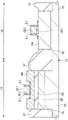
The steps of manufacturing the semiconductor device according to this embodiment will be described with reference to the drawings. Fig. 1 and 2 are process flow charts showing steps of manufacturing a semiconductor device according to an embodiment of the present invention. Fig. 3 to 38 are a main part cross sectional view or a main part plan view in the manufacturing process of the semiconductor device according to the embodiment of the present invention. In fig. 3 to 38, fig. 3 to 23 and fig. 26 to 38 are main part sectional views, and fig. 24 and 25 are main part plan views.
First, as shown in fig. 3, an SOI (Silicon On Insulator) substrate 1 is prepared (step S1 of fig. 1).
The SOI substrate 1 has: a semiconductor substrate (support substrate) SB as a support substrate, an insulating layer (buried insulating film) BX formed on a main surface of the semiconductor substrate SB, and a semiconductor layer SM formed on an upper surface of the insulating layer BX.
The semiconductor substrate SB is a support substrate that supports the insulating layer BX and a structure located above the insulating layer BX, but may also be a semiconductor substrate. Semiconductor substrate SB is preferably a single crystal silicon substrate, and is made of p-type single crystal silicon, for example. For example, the semiconductor substrate SB can be formed from single crystal silicon having a resistivity of about 1 to 10 Ω cm. The thickness of the semiconductor substrate SB can be set to, for example, about 700 to 750 μm. The insulating layer BX is preferably a silicon oxide film, and the thickness of the insulating layer BX can be, for example, about 10 to 20 nm. In the case where the insulating layer BX is a silicon Oxide film, the insulating layer BX can be regarded as a Buried Oxide film, i.e., a BOX (Buried Oxide) layer. The semiconductor layer SM is made of single crystal silicon or the like. For example, the semiconductor layer SM can be formed using single crystal silicon having a resistivity of about 1 to 10 Ω cm. The thickness of the semiconductor layer SM is thinner than that of the semiconductor substrate SB as a support substrate, and the thickness of the semiconductor layer SM can be set to, for example, about 15 to 25 nm. The SOI substrate 1 is formed of the semiconductor substrate SB, the insulating layer BX, and the semiconductor layer SM.
The SOI substrate 1 includes an SOI region 1A and a bulk region 1B (bulk region), the SOI region 1A is a region (planar region) in which the SOI structure is maintained until the semiconductor device is completed, and the bulk region 1B is a region (planar region) in which the semiconductor layer SM and the insulating layer BX are removed and which is not the SOI structure. The SOI region 1A and the body region 1B are regions (planar regions) different from each other. In the case of the SOI structure, a silicon layer (single crystal silicon layer) is preferably used as the semiconductor layer over the insulating layer, but the present invention is not limited thereto, and a semiconductor layer other than single crystal silicon may be used.
In the SOI substrate 1, a main surface of the semiconductor substrate SB on a side contacting the insulating layer BX is referred to as an upper surface of the semiconductor substrate SB, and a main surface of the semiconductor substrate SB on a side opposite to the upper surface is referred to as a rear surface of the semiconductor substrate SB. In the SOI substrate 1, a main surface of the insulating layer BX on a side in contact with the semiconductor substrate SB is referred to as a lower surface of the insulating layer BX, a main surface of the insulating layer SM on a side in contact with the semiconductor layer SM is referred to as an upper surface of the insulating layer BX, and the upper surface and the lower surface of the insulating layer are surfaces on opposite sides to each other. The principal surface of the semiconductor layer SM on the side in contact with the insulating layer BX is referred to as the lower surface of the semiconductor layer SM, and the principal surface of the semiconductor layer SM on the side opposite to the lower surface is referred to as the upper surface of the semiconductor layer SM.
The method for manufacturing the SOI substrate 1 is not limited, but can be manufactured by, for example, the SIMOX (Silicon Implanted Oxide: separation by oxygen implantation). In the SIMOX method, O is ion-implanted at high energy into a main surface of a semiconductor substrate made of silicon (Si) 2 (oxygen), si (silicon) is bonded to oxygen in the subsequent heat treatment, and an insulating layer BX made of silicon oxide is formed at a position slightly deeper than the surface of the semiconductor substrate. At this time, a thin film of silicon (Si) remaining on the insulating layer BX becomes the semiconductor layer SM, and a semiconductor substrate under the insulating layer BX becomes the semiconductor substrate SB. Alternatively, the SOI substrate 1 may be formed by a bonding method. In the bonding method, for example, an insulating layer BX is formed by oxidizing a surface of a first semiconductor substrate made of silicon (Si), and then a second semiconductor substrate made of silicon (Si) is bonded to the first semiconductor substrate by pressure bonding at a high temperature, and then the second semiconductor substrate is thinned. At this time, the thin film of the second semiconductor substrate remaining on the insulating layer BX becomes the semiconductor layer SM, and the first semiconductor substrate under the insulating layer BX becomes the semiconductor substrate SB. The SOI substrate 1 can also be manufactured using other methods, such as a Smart cut process (Smart cut process), for example.
Next, as shown in fig. 4, an insulating film (pad insulating film) ZM1 is formed on the main surface of the SOI substrate 1, that is, on the upper surface of the semiconductor layer SM (step S2 of fig. 1). The insulating film ZM1 is made of the same material as the insulating layer BX. In the case where the insulating layer BX is made of silicon oxide, the insulating film ZM1 is also made of silicon oxide. The insulating film ZM1 can be formed by, for example, a CVD (Chemical Vapor Deposition) method or the like. The thickness of the insulating film ZM1 is preferably set to a total value of the thickness of the insulating layer BX and the etching thickness (etching amount) of the insulating film ZM1 in the SOI region 1A in step S10 described later.
Next, an insulating film ZM2 is formed on the insulating film ZM1 (step S3 in fig. 1). The insulating film ZM2 is made of a material different from that of the insulating film ZM1. When the insulating layer BX and the insulating film ZM1 are made of silicon oxide, the insulating film ZM2 is preferably made of silicon nitride. The insulating film ZM2 is made of a material different from that of the insulating film ZM3 described later. The insulating film ZM2 can be formed by CVD or the like, for example. The thickness of the insulating film ZM2 can be, for example, about 80 to 120 nm.
Through the steps (steps S1 to S3) thus far, a substrate was prepared as follows: the semiconductor device comprises a semiconductor substrate SB, an insulating layer BX on the semiconductor substrate SB, a semiconductor layer SM on the insulating layer BX, an insulating film ZM1 on the semiconductor layer SM, and an insulating film ZM2 on the insulating film ZM1.
Next, as shown in fig. 5, the trench TR is formed (step S4 of fig. 1). The trench TR is a trench for forming an element isolation region ST described later, that is, a trench for element isolation.
The trench TR can be formed as follows. That is, first, a photoresist pattern (not shown) is formed on the insulating film ZM2 by a photolithography technique. The photoresist pattern has such a pattern (planar shape): the insulating film ZM2 in the region where the trench TR is to be formed is exposed and the insulating film ZM2 in the region other than the region is covered. Then, the insulating film ZM2 is etched (preferably dry etched) using the photoresist pattern as an etching mask to be patterned. Thereby, the insulating film ZM2 in the region where the trench TR is to be formed is selectively removed. Then, after the photoresist pattern is removed, the insulating film ZM1, the semiconductor layer SM, the insulating layer BX, and the semiconductor substrate SB are etched (preferably dry-etched) using the insulating film ZM2 as an etching mask (hard mask), whereby the trench TR can be formed.
The trench TR penetrates the insulating film ZM2, the insulating film ZM1, the semiconductor layer SM, and the insulating layer BX, and the bottom (bottom surface) of the trench TR reaches the semiconductor substrate SB. That is, the bottom (bottom) of the trench TR is located halfway through the thickness of the semiconductor substrate SB. Therefore, the bottom surface of the trench TR is located below the lower surface of the insulating layer BX, and the semiconductor substrate SB is exposed at the bottom of the trench TR. The depth of the trench TR may be, for example, about 250 to 300 nm.
Next, as shown in fig. 6, an insulating film ZM3 is formed on the insulating film ZM2 so as to fill the trench TR (step S5 in fig. 1). The insulating film ZM3 is an insulating film for forming the element isolation region ST, and is preferably a silicon oxide film. Therefore, the insulating film ZM3, the insulating film ZM1, and the insulating layer BX are made of the same material, and preferably, are made of silicon oxide. The insulating film ZM3 can be formed by CVD or the like. The thickness of the insulating film ZM3 is preferably set to a thickness sufficient to fill (fill) the trench TR with the insulating film ZM3.
Next, as shown in fig. 7, the insulating film ZM3 is polished (polished) by CMP (Chemical Mechanical Polishing) or the like to remove the insulating film ZM3 outside the trench TR and leave the insulating film ZM3 in the trench TR (step S6 in fig. 1). As a result, as shown in fig. 7, the element isolation region ST formed of the insulating film ZM3 buried in the trench TR can be formed. The element isolation region ST is formed in the trench TR.
When the polishing process of step S6 is performed, the insulating film ZM2 functions as a polishing stopper film. That is, in step S6, the insulating film ZM2 can be made to function as a polishing stopper film by performing the polishing treatment under the condition that the insulating film ZM2 is less likely to be polished than the insulating film ZM3. In other words, in step S6, the insulating film ZM2 can be made to function as a polishing stopper film by performing the polishing treatment under the condition that the polishing rate of the insulating film ZM2 is lower (slower) than the polishing rate of the insulating film ZM3. In order to allow the insulating film ZM2 to function as a polishing barrier film, it is necessary to form the insulating film ZM2 from a material different from that of the insulating film ZM3. When the insulating film ZM3 is made of silicon oxide, the insulating film ZM2 is preferably made of silicon nitride. At the end of the polishing process in step S6, the upper surface of the insulating film ZM2 is exposed, and the element isolation region ST is buried in the trench TR, but as shown in fig. 7, the upper surface of the element isolation region ST is located at substantially the same height as the upper surface of the insulating film ZM2.
Next, as shown in fig. 8, the upper surface of the element isolation region ST is wet-etched, thereby lowering the height position of the upper surface of the element isolation region ST (step S7 of fig. 1). Thus, the height of the upper surface of the element isolation region ST is lower than the upper surface of the insulating film ZM2 by a predetermined distance (distance in the height direction). In the wet etching at this time, hydrofluoric acid (hydrofluoric acid) is preferably used. At the end of the wet etching, the height of the upper surface of the element isolation region ST is lower than the upper surface of the insulating film ZM2, but is substantially the same as the height of the upper surface of the insulating film ZM1 or higher than the upper surface of the insulating film ZM1, and more preferably higher than the upper surface of the insulating film ZM1.
In addition, in the present application, when "hydrofluoric acid" is mentioned, dilute hydrofluoric acid (dilute hydrofluoric acid) is also included.
Next, as shown in fig. 9, the insulating film ZM2 is removed by etching (step S8 of fig. 1). In this case, the insulating film ZM1 can function as an etching stopper film. In step S8, the insulating film ZM2 is preferably removed by etching under the condition that the insulating film ZM1 and the element isolation region ST are less likely to be etched than the insulating film ZM2. In other words, the insulating film ZM2 is preferably removed by etching under the condition that the etching rate of each of the insulating film ZM1 and the element isolation region ST is lower than the etching rate of the insulating film ZM2. This makes it possible to selectively etch and remove the insulating film ZM2 while suppressing or preventing the etching of the insulating film ZM1 and the element isolation region ST.
Further, a small etching rate (etching rate) is synonymous with a slow etching rate, and is also synonymous with a low etching rate. The high etching rate is synonymous with the high etching rate, and is also synonymous with the high etching rate. In the case of easy etching, the etching rate is high, and in the case of difficult etching, the etching rate is low.
In addition, in the etching in step S8, wet etching is preferably used. When the insulating film ZM2 is made of silicon nitride and the insulating film ZM1 and the element isolation region ST are made of silicon oxide, hot phosphoric acid (heated phosphoric acid) is preferably used as an etching solution used in the wet etching in step S8. When the insulating film ZM2 is removed by etching in step S8, the upper surface of the insulating film ZM1 is exposed. That is, in step S8, the insulating film ZM2 is removed to expose the upper surface of the insulating film ZM1 in both the SOI region 1A and the body region 1B.
In this way, the device isolation region ST of the STI structure can be formed by the STI (shallow trench isolation) method. In the stage of preparing the SOI substrate 1, the semiconductor layer SM is formed on the entire upper surface of the semiconductor substrate SB with the insulating layer BX interposed therebetween, but once the element isolation region ST is formed, the semiconductor layer SM is divided into a plurality of regions (active regions) each surrounded by the element isolation region ST.
The trench TR and the element isolation region ST filling the trench TR penetrate the insulating film ZM1, the semiconductor layer SM, and the insulating layer BX, and the bottom thereof reaches the semiconductor substrate SB, and the lower portion of the element isolation region ST is located in the semiconductor substrate SB. Namely, the following states are obtained: the element isolation region ST is buried in a trench TR formed across the insulating film ZM1, the semiconductor layer SM, the insulating layer BX, and the semiconductor substrate SB. Therefore, a part of the element isolation region ST is located below the lower surface of the insulating layer BX. That is, the bottom surface (lower surface) of the isolation region ST is located deeper than the lower surface of the insulating layer BX, and a part (lower part) of the isolation region ST protrudes downward from the lower surface of the insulating layer BX.
At this stage, the SOI region 1A and the body region 1B have the same structure. That is, the SOI region 1A and the body region 1B have a structure in which the insulating layer BX, the semiconductor layer SM, and the insulating film ZM1 are stacked in this order from bottom to top on the semiconductor substrate SB. In a plan view, an element isolation region ST is interposed (arranged) between the SOI region 1A and the body region 1B. In other words, the element isolation region ST is arranged at the boundary between the SOI region 1A and the body region 1B in a plan view.
Next, as shown in fig. 10, a photoresist pattern (resist pattern, mask layer) PR1 which covers the SOI region 1A and exposes the body region 1B is formed as a mask layer on the insulating film ZM1 by photolithography. The insulating film ZM1 of the SOI region 1A is covered with the photoresist pattern PR1, and the insulating film ZM1 of the bulk region 1B is not covered with the photoresist pattern PR1 but is exposed. An end portion (side surface) of the photoresist pattern PR1 is located on an element isolation region ST provided between the SOI region 1A and the body region 1B.
Further, the photolithography technique is a technique as follows: a photoresist film is formed on the entire main surface of a semiconductor substrate by a coating method or the like, and then the photoresist film is exposed to light and developed to be patterned, thereby obtaining a desired photoresist pattern.
Next, as shown in fig. 11, the insulating film ZM1 of the body region 1B is removed by etching using the photoresist pattern PR1 as an etching mask (step S9 of fig. 2). In step S9, the insulating film ZM1 is preferably removed by etching under the condition that the semiconductor layer SM is less likely to be etched than the insulating film ZM1. In other words, in step S9, the insulating film ZM1 is preferably removed by etching under the condition that the etching rate of the semiconductor layer SM is lower (slower) than the etching rate of the insulating film ZM1. Thus, the insulating film ZM1 in the body region 1B can be removed by etching, and the semiconductor layer SM can function as an etching stopper layer. In the etching in step S9, wet etching is preferably used. When the insulating film ZM1 is made of silicon oxide, hydrofluoric acid is preferably used as the etching liquid used for the wet etching in step S9. In the body region 1B, after the insulating film ZM1 is removed by etching, the upper surface of the semiconductor layer SM is exposed. On the other hand, in the SOI region 1A, the insulating film ZM1 is covered with the photoresist pattern PR1 and thus is not etched but left. In addition, the region covered with the photoresist pattern PR1 in the element isolation region ST is not etched, and the region exposed without being covered with the photoresist pattern PR1 in the element isolation region ST can be etched by the same degree as the etching thickness (etching amount) of the insulating film ZM1 in the body region 1B. Thereafter, as shown in fig. 12, the photoresist pattern PR1 is removed by ashing (ashing) or the like.
At this stage, as shown in fig. 12, the insulating film ZM1 is left in the SOI region 1A and the upper surface of the insulating film ZM1 is exposed, while the insulating film ZM1 is removed and the upper surface of the semiconductor layer SM is exposed in the bulk region 1B.
Next, as shown in fig. 13, the semiconductor layer SM of the body region 1B is removed by etching (step S10 of fig. 2). In this step S10, the semiconductor layer SM in the body region 1B is preferably removed by etching under the condition that the insulating layer BX, the insulating film ZM1, and the element isolation region ST are less likely to be etched than the semiconductor layer SM. In other words, in step S10, the semiconductor layer SM in the body region 1B is preferably removed by etching under the condition that the etching rates of the insulating layer BX, the insulating film ZM1, and the element isolation region ST are lower (slower) than the etching rate of the semiconductor layer SM. This makes it possible to remove the semiconductor layer SM in the body region 1B by etching, to make the insulating layer BX of the body region 1B function as an etching stopper, and to suppress or prevent the etching of the element isolation region ST and the insulating film ZM1 in the SOI region 1A. In addition, wet etching can be preferably used in the etching in step S10. When the semiconductor layer SM is made of silicon and the insulating layer BX, the insulating film ZM1, and the element isolation region ST are made of silicon oxide, an APM solution (ammonia Hydrogen-oxide Mixture) is preferably used as an etching solution used in the wet etching in step S10. The APM solution corresponds to a mixture of ammonia and hydrogen peroxide. In the body region 1B, after the semiconductor layer SM is removed by etching, the upper surface of the insulating layer BX is exposed. On the other hand, in the SOI region 1A, the semiconductor layer SM is covered with the insulating film ZM1 and thus is not etched but remains.
The etching in step S10 is performed in a state where the upper surface of the semiconductor layer SM in the body region 1B, the upper surface of the insulating film ZM1 in the SOI region 1A, and the upper surface of the element isolation region ST are exposed. Therefore, when the semiconductor layer SM of the body region 1B is etched in step S10, the surface layer portion of the insulating film ZM1 of the SOI region 1A may be slightly etched, but in such a case, the insulating film ZM1 of the SOI region 1A is also left in a layer form at the end of the etching in step S10, and the semiconductor layer SM of the SOI region 1A is not exposed. That is, even if the insulating film ZM1 of the SOI region 1A is etched in step S10, the etching amount (etching thickness) of the insulating film ZM1 is smaller than the thickness of the insulating film ZM1 of the SOI region 1A before step S10 is performed. In step S10, the element isolation region ST may be etched by the same amount (etching thickness) as the insulating film ZM1 in the SOI region 1A.
At this stage, as shown in fig. 13, in the SOI region 1A, the insulating film ZM1 is left in a layered state and the upper surface of the insulating film ZM1 is exposed, while in the bulk region 1B, the insulating film ZM1 and the semiconductor layer SM are removed and the upper surface of the insulating layer BX is exposed.
Next, as shown in fig. 14, the insulating film ZM1 of the SOI region 1A and the insulating layer BX of the bulk region 1B are etched to reduce the thickness of each of the insulating film ZM1 of the SOI region 1A and the insulating layer BX of the bulk region 1B (step S11 of fig. 2). Wet etching can be preferably used in the etching of step S11.
Fig. 13 shows a stage after the etching in step S10 is completed and before the etching in step S11 is performed; fig. 14 shows a stage after the etching step of step S11 is completed.
Since the etching targets are different in step S10 and step S11, the etching liquid used in step S11 is different from the etching liquid used in step S10. That is, step S10 is a step of actively (intentionally) etching the semiconductor layer SM of the body region 1B, whereas step S11 is a step of actively (intentionally) etching the insulating film ZM1 of the SOI region 1A and the insulating layer BX of the body region 1B.
In step S10, since the semiconductor layer SM is to be etched, an etching solution that can easily etch the semiconductor layer SM, that is, an etching solution in which the etching rate of the semiconductor layer SM is increased to some extent, is used. On the other hand, in step S11, since the insulating film ZM1 and the insulating layer BX are to be etched, an etching solution that easily etches the insulating film ZM1 and the insulating layer BX, that is, an etching solution having a somewhat large etching rate of the insulating film ZM1 and the insulating layer BX is used.
Therefore, the etching rates of the insulating film ZM1 and the insulating layer BX when the etching solution used in step S11 is used are higher (faster) than the etching rates of the insulating film ZM1 and the insulating layer BX when the etching solution used in step S10 is used. That is, the etching rates of the insulating film ZM1 of the SOI region 1A and the insulating layer BX of the body region 1B in the etching step of step S11 are higher (faster) than the etching rates of the insulating film ZM1 of the SOI region 1A and the insulating layer BX of the body region 1B in the etching step of step S10. Since the insulating film ZM1 and the insulating layer BX are made of the same material (preferably, silicon oxide), the etching rate of the insulating film ZM1 in step S11 is substantially the same as the etching rate of the insulating layer BX, and the etching rate of the insulating film ZM1 in step S10 is substantially the same as the etching rate of the insulating layer BX.
In the etching step of step S10, since an etching solution is used in which the semiconductor layer SM is more easily etched than the insulating layer BX and the insulating film ZM1, the etching rate of each of the insulating layer BX and the insulating film ZM1 is lower (slower) than the etching rate of the semiconductor layer SM. On the other hand, in the etching step of step S11, the insulating layer BX and the insulating film ZM1 are etched with the aim of using an etching solution in which the insulating layer BX and the insulating film ZM1 are etched more easily than the semiconductor layer SM, that is, an etching solution in which the etching rates of the insulating layer BX and the insulating film ZM1 are higher (faster) than the etching rate of the semiconductor layer SM.
When the insulating film ZM1 and the insulating layer BX are made of silicon oxide, hydrofluoric acid can be preferably used as the etching solution used in the wet etching in step S11.
The etching in step S11 is performed to reduce the thickness of the insulating film ZM1 in the SOI region 1A and the thickness of the insulating layer BX in the body region 1B. Therefore, the etching in step S11 is completed before the entire thickness of the insulating film ZM1 is removed and the semiconductor layer SM is exposed in the SOI region 1A, and is completed before the entire thickness of the insulating layer BX is removed and the semiconductor substrate SB is exposed in the bulk region 1B. Therefore, immediately before the etching in step S11, immediately after the etching in step S11 is performed, the insulating layer ZM1 is left in a layer shape in the SOI region 1A and the insulating layer BX is left in a layer shape in the body region 1B. Therefore, immediately before the etching in step S11, immediately after the etching in step S11 is performed, neither the semiconductor layer SM nor the semiconductor substrate SB is exposed in the SOI region 1A nor the body region 1B.
The thickness T3 of the insulating film ZM1 in the SOI region 1A immediately after the etching in step S11 is thinner than the thickness T1 of the insulating film ZM1 in the SOI region 1A immediately before the etching in step S11 (i.e., 0 < T3 < T1). The thickness T4 of the insulating layer BX of the body region 1B immediately after the etching in step S11 is smaller than the thickness T2 of the insulating layer BX of the body region 1B immediately before the etching in step S11 (i.e., 0 < T4 < T2).
The structure immediately before the etching in step S11 corresponds to fig. 13; the structure immediately after the etching in step S11 is performed corresponds to fig. 14. Therefore, the thickness T1 of the insulating film ZM1 in the SOI region 1A and the thickness T2 of the insulating layer BX in the bulk region 1B immediately before the etching in step S11 are shown in fig. 13, and the thickness T3 of the insulating film ZM1 in the SOI region 1A and the thickness T4 of the insulating layer BX in the bulk region 1B immediately after the etching in step S11 are shown in fig. 14.
Since the etching in step S11 is performed in a state where the upper surface of the element isolation region ST, the upper surface of the insulating film ZM1 of the SOI region 1A, and the upper surface of the insulating layer BX of the body region 1B are exposed, the surface layer portion of the element isolation region ST, the surface layer portion of the insulating film ZM1 of the SOI region 1A, and the surface layer portion of the insulating layer BX of the body region 1B are removed by the etching in step S11. However, the etching amount (etching thickness) of the insulating film ZM1 in the SOI region 1A in step S11 is smaller than the thickness T1 of the insulating film ZM1 in the SOI region 1A immediately before step S11; the etching amount (etching thickness) of the insulating layer BX of the body region 1B in step S11 is smaller than the thickness T2 of the insulating layer BX of the body region 1B immediately before step S11. Therefore, even if step S11 is performed, the state where the insulating film ZM1 is layered on the semiconductor layer SM in the SOI region 1A and the insulating layer BX is layered on the semiconductor substrate SB in the body region 1B is maintained, the semiconductor layer SM is not exposed in the SOI region 1A, and the semiconductor substrate SB is not exposed in the body region 1B. In step S11, the element isolation region ST can be etched by the same amount (etching thickness) as the insulating film ZM1 in the SOI region 1A.
Next, as shown in fig. 15, a photoresist pattern (resist pattern, mask layer) PR2 that covers the body region 1B and exposes the SOI region 1A is formed as a mask layer on the SOI substrate 1 by photolithography. Although the insulating layer BX of the body region 1B is covered with the photoresist pattern PR2, the insulating film ZM1 of the SOI region 1A is not covered with the photoresist pattern PR2 but is exposed. An end portion (side surface) of the photoresist pattern PR2 is located on the element isolation region ST arranged at the boundary between the SOI region 1A and the body region 1B.
Next, using the photoresist pattern PR2 as a mask (ion implantation blocking mask), ion implantation for threshold adjustment is performed on the semiconductor substrate SB of the SOI region 1A (step S12 of fig. 2). The ion implantation performed in this step S12, hereinafter referred to as ion implantation P1, is schematically shown by arrows in fig. 15. In fig. 15, a region into which an impurity is introduced by ion implantation P1 is denoted by a semiconductor region (impurity diffusion layer) GP with reference numeral GP. By the ion implantation P1 in step S12, impurities are introduced into the semiconductor substrate SB of the SOI region 1A, thereby forming a semiconductor region GP.
The ion implantation P1 is ion implantation for controlling a threshold voltage (threshold value) of a MISFET formed later in the SOI region 1A. In the ion implantation P1, it is desirable that impurity ions be introduced into the semiconductor substrate SB of the SOI substrate 1 in the SOI region 1A, but impurity ions not be introduced into the semiconductor layer SM of the SOI substrate 1. In addition, in the ion implantation P1, since the photoresist pattern PR2 functions as an ion implantation blocking mask, impurities are not introduced into the body region 1B of the SOI substrate 1, and therefore, impurities are not introduced into the semiconductor substrate SB and the semiconductor layer SM in the body region 1B.
In the ion implantation P1, it is preferable not to implant impurity ions into the semiconductor layer SM of the SOI region 1A, because if the impurity ions are implanted into the semiconductor layer SM of the SOI region 1A in the ion implantation P1, the electrical characteristics of the MISFET formed in the SOI region 1A later may be varied.
Therefore, it is preferable to perform the ion implantation P1 at a high implantation energy that enables impurity ions to penetrate the semiconductor layer SM. The implantation energy of the ion implantation P1 is adjusted according to the thickness of the insulating film ZM1, the thickness of the semiconductor layer SM, and the thickness of the insulating layer BX, and is set so that at least the range of impurity ions (range) is located within the semiconductor substrate SB. Thus, in the ion implantation P1, impurity ions can be implanted into the semiconductor substrate SB of the SOI region 1A without implanting impurity ions into the semiconductor layer SM of the SOI region 1A.
In the ion implantation P1, it is preferable that in the SOI region 1A, an impurity is ion-implanted into the semiconductor substrate SB below the insulating layer BX, and an impurity ion is also ion-implanted into a region in the semiconductor substrate SB in the vicinity of the insulating layer BX (a region adjacent to the insulating layer BX). That is, the semiconductor region GP formed in the semiconductor substrate SB is preferably brought into contact with (adjacent to) the insulating layer BX. The impurity concentration of the semiconductor region GP can be adjusted by the implantation amount (dose) of the ion implantation P1, thereby controlling the threshold of the MISFET formed in the SOI region 1A after that. Therefore, in the manufactured semiconductor device, impurities are introduced into a region (corresponding to the semiconductor region GP) adjacent to the insulating layer BX in the semiconductor substrate SB of the SOI region 1A. After the ion implantation P1, the photoresist pattern PR2 is removed.
In the ion implantation P1 of step S12, it is preferable that impurity ions are not implanted into the semiconductor layer SM of the SOI substrate 1 as much as possible, but for this reason, the ion implantation energy becomes considerably high. The dose of the ion implantation P1 is also quite large, for example, about 10 times the dose of the general channel doping ion implantation. For example, the dose of the ion implantation P1 is 1 × 10 12 ~1×10 14 /cm 2 Left and right. Therefore, in the ion implantation P1, a considerable amount of impurity ions are implanted also into the element isolation region ST in the portion not covered with the photoresist pattern PR2. That is, in the ion implantation P1, a considerable amount of impurity ions are implanted into the element isolation region ST in the region adjacent to the semiconductor layer SM of the SOI region 1A in a plan view. If impurity ions are implanted during the ion implantation, the element isolation region ST is easily etched, and the etching rate is easily increased in the etching step of step S14 to be performed later. However, in the present embodiment, since the thickness of each of the insulating film ZM1 of the SOI region 1A and the insulating film BX of the body region 1B is already reduced in the etching step of step S11, the etching amount can be suppressed in step S14 to be described later, and thereby, the element isolation region ST can be prevented from being over-etched. Therefore, in step S14 described later, the formation of a recess (divot) DT described later in the element isolation region ST can be suppressed or prevented.
Since the ion implantation step is not performed on the SOI substrate 1 after the element isolation region ST is formed in step S6 and before the etching step of step S11 is completed, the etching step of step S10 and the etching step of step S11 are performed in a state where no impurity is ion-implanted into the element isolation region ST. On the other hand, since the ion implantation step (steps S12 and S13) is performed on the SOI substrate 1 after the etching step of step S11 and before the etching step of step S14, the etching step of step S14 is performed in a state where the impurity is ion-implanted also in the element isolation region ST.
In addition, in the ion implantation P1, a P-type impurity (for example, boron or the like) or an n-type impurity (for example, phosphorus, arsenic or the like) is ion-implanted. When a P-type impurity is ion-implanted by ion implantation P1, the semiconductor region GP is a P-type semiconductor region into which the P-type impurity is introduced. In addition, when the n-type impurity is ion-implanted by ion implantation P1, the semiconductor region GP is an n-type semiconductor region into which the n-type impurity is introduced. In the case where the MISFET formed in the SOI region 1A is an n-channel type MISFET, it is more preferable that the impurity implanted by ion implantation of P1 be a P-type impurity. Thus, even when impurity ions are implanted into not only the semiconductor substrate SB but also the semiconductor layer SM in the ion implantation P1, the associated problems are less likely to occur.
The semiconductor region GP is formed to control the threshold voltage of the MISFET formed in the SOI region 1A. In the manufactured semiconductor device, by applying a predetermined voltage (potential) to the semiconductor region GP formed on the semiconductor substrate SB of the SOI region 1A, the threshold voltage of the MISFET formed on the SOI region 1A can be controlled.
In addition, it is not desirable to directly form a photoresist pattern on the surface (silicon surface) of the semiconductor layer SM or the surface (silicon surface) of the semiconductor substrate SB. In this embodiment, since the photoresist pattern PR2 is formed in a state where the semiconductor layer SM and the semiconductor substrate SB are not exposed and the photoresist pattern PR2 is formed on the element isolation region ST and on the insulating layer BX of the body region 1B, the photoresist pattern PR2 does not need to be in contact with the surface (silicon surface) of the semiconductor substrate SB and the surface (silicon surface) of the semiconductor layer SM. Since the photoresist pattern PR1 is formed in a state where the semiconductor layer SM and the semiconductor substrate SB are not exposed and the photoresist pattern PR1 is formed on the element isolation region ST and on the insulating film ZM1 in the SOI region 1A, the photoresist pattern PR1 does not need to be in contact with the surface (silicon surface) of the semiconductor substrate SB and the surface (silicon surface) of the semiconductor layer SM. Since the photoresist pattern PR3 described later is formed in a state where the semiconductor layer SM and the semiconductor substrate SB are not exposed and the photoresist pattern PR3 described later is formed on the element isolation region ST and on the insulating film ZM1 in the SOI region 1A, the photoresist pattern PR3 described later may not contact the surface (silicon surface) of the semiconductor substrate SB and the surface (silicon surface) of the semiconductor layer SM.
At the end of step S12, in the SOI region 1A, the insulating film ZM1 is kept in a layered state and the upper surface of the insulating film ZM1 is exposed, and in the bulk region 1B, the insulating layer BX is kept in a layered state and the upper surface of the insulating layer BX is exposed. In the SOI region 1A, the semiconductor layer SM is not exposed, and in the body region 1B, the semiconductor substrate SB is not exposed.
Next, as shown in fig. 16, a photoresist pattern (resist pattern, mask layer) PR3 that covers the SOI region 1A and exposes the body region 1B is formed as a mask layer on the SOI substrate 1 by photolithography. The insulating film ZM1 of the SOI region 1A is covered with the photoresist pattern PR3, but the insulating layer BX of the bulk region 1B is not covered with the photoresist pattern PR3 but is exposed. An end (side) of the photoresist pattern PR3 is located on the element isolation region ST.
Next, a p-type impurity (e.g., boron or the like) is ion-implanted into the semiconductor substrate SB of the body region 1B using the photoresist pattern PR3 as a mask (ion implantation blocking mask), thereby forming a p-type well PW (step S13 of fig. 2).
In the ion implantation for forming the p-type well PW, the photoresist pattern PR3 functions as an ion implantation blocking mask, and therefore, impurities are not introduced into the SOI region 1A of the SOI substrate 1, and therefore, impurities are not introduced into the semiconductor layer SM and the semiconductor substrate SB in the SOI region 1A. A p-type well PW is formed in the semiconductor substrate SB of the body region 1B. After the ion implantation of step S13, as shown in fig. 17, the photoresist pattern PR3 is removed.
Alternatively, the semiconductor substrate SB of the body region 1B may be subjected to channel doping ion implantation using the photoresist pattern PR3 as a mask (ion implantation preventing mask) before or after ion implantation for forming the p-type well PW.
Although the case where step S13 is executed after step S12 is described here, the order of step S12 and step S13 may be reversed, and step S13 may be executed before step S12 is executed, and then step S12 may be executed. In this case, after the etching process of step S11, the photoresist pattern PR3 forming process, the ion implantation (P-type well PW forming process) of step S13, the photoresist pattern PR3 removing process, the photoresist pattern PR2 forming process, the ion implantation P1 (semiconductor region GP forming process) of step S12, and the photoresist pattern PR2 removing process are sequentially performed.
Next, as shown in fig. 18, the insulating film ZM1 of the SOI region 1A and the insulating layer BX of the body region 1B are removed by etching (step S14 of fig. 2).
In step S14, the insulating film ZM1 of the SOI region 1A and the insulating layer BX of the body region 1B are preferably removed by etching under the condition that the semiconductor layer SM and the semiconductor substrate SB are less susceptible to etching than the insulating film ZM1 and the insulating layer BX. In other words, in step S14, the insulating film ZM1 of the SOI region 1A and the insulating layer BX of the body region 1B are preferably removed by etching under the condition that the etching rate of the semiconductor layer SM and the etching rate of the semiconductor substrate SB are lower than the etching rate of the insulating film ZM1 and the etching rate of the insulating layer BX. Thus, the insulating film ZM1 of the SOI region 1A and the insulating layer BX of the body region 1B can be removed by etching, and the semiconductor layer SM of the SOI region 1A and the semiconductor substrate SB of the body region 1B can be made to function as an etching stopper, thereby suppressing or preventing the semiconductor layer SM of the SOI region 1A and the semiconductor substrate SB of the body region 1B from being etched.
In the etching of step S14, wet etching can be preferably used. The etching targets in step S11 and step S14 are common, and the insulating film ZM1 and the insulating layer BX are used as the etching targets in step S14. Therefore, in the etching in step S14, the same kind of etching liquid as that used in step S11 can be used. In the case where the insulating film ZM1 and the insulating layer BX are made of silicon oxide, hydrofluoric acid can be preferably used as the etching solution in step S14, similarly to step S11. In the case where hydrofluoric acid is used as each of the etching liquid in step S11 and the etching liquid in step S14, the concentration of hydrofluoric acid may be the same or different between step S11 and step S14.
That is, the same kind of etching liquid as that used in step S11 is used in the etching in step S14, which means that hydrofluoric acid is also used in step S14 when the etching liquid used in step S11 is hydrofluoric acid; the concentration of the etching solution (herein, the concentration of hydrofluoric acid) may be different between step S11 and step S14. That is, the same kind of etching solution means the same kind of etching solution, and includes not only the case where the concentration of the etching solution is the same but also the case where the concentration of the etching solution is different.
Since the etching in step S14 is performed in a state where the upper surface of the element isolation region ST, the upper surface of the insulating film ZM1 of the SOI region 1A, and the upper surface of the insulating layer BX of the body region 1B are exposed, the surface layer portion of the element isolation region ST, the insulating film ZM1 of the SOI region 1A, and the insulating layer BX of the body region 1B are removed by etching in step S14. The etching in step S14 is terminated at the stage of removing the insulating film ZM1 in the SOI region 1A to expose the upper surface of the semiconductor layer SM and removing the insulating layer BX in the body region 1B to expose the upper surface of the semiconductor substrate SB. In step S14, the element isolation region ST may be etched by the same amount (etching thickness) as the etching amounts of the insulating film ZM1 in the SOI region 1A and the insulating layer BX in the body region 1B.
At the end of step S14, as shown in fig. 18, the insulating layer ZM1 is removed to expose the upper surface of the semiconductor layer SM in the SOI region 1A, and the insulating layer BX is removed to expose the upper surface of the semiconductor substrate SB (p-type well PW) in the body region 1B.
Thus, the element isolation region ST is formed on the SOI substrate 1, the semiconductor layer SM and the insulating layer BX are removed in the body region 1B to expose the upper surface of the semiconductor substrate SB (no longer having an SOI structure), and the SOI structure (a stacked structure of the semiconductor substrate SB, the insulating layer BX, and the semiconductor layer SM) is maintained in the SOI region 1A with the semiconductor layer SM and the insulating layer BX left. In addition, a semiconductor region GP for threshold adjustment is formed in the semiconductor substrate SB of the SOI region 1A.
The SOI substrate 1 at this stage is referred to as a substrate 1C. Here, the body region 1B of the substrate 1C is formed of the semiconductor substrate SB with the semiconductor layer SM and the insulating layer BX removed; the SOI region 1A of the substrate 1C is maintained as an SOI structure (a laminated structure of the semiconductor substrate SB, the insulating layer BX, and the semiconductor layer SM). Hereinafter, the main surface of the substrate 1C is synonymous with the main surface of the semiconductor layer SM of the SOI region 1A and the main surface of the semiconductor substrate SB of the bulk region 1B. The substrate 1C has the SOI region 1A and the body region 1B, but the SOI region 1A can be regarded as a region having an SOI structure in which the insulating layer BX is buried, and the body region 1B can be regarded as a region having no SOI structure in which the insulating layer BX is not buried. Specifically, the SOI region 1A of the substrate 1C is a region having a laminated structure (SOI structure) in which the semiconductor substrate SB, the insulating layer BX on the semiconductor substrate SB, and the semiconductor layer SM on the insulating layer BX are laminated, and the bulk region 1B of the substrate 1C is a region composed of the semiconductor substrate SB throughout the entire thickness thereof. However, the SOI region 1A and the bulk region 1B may include a region where the element isolation region ST exists. In the body region 1B, after the semiconductor layer SM and the insulating layer BX are removed, a part of the element isolation region ST (a part located below the lower surface of the insulating layer BX) remains in a state of being buried in the semiconductor substrate SB, which becomes the element isolation region ST of the body region 1B.
Next, semiconductor elements such as MISFETs (transistors) are formed in the SOI region 1A and the body region 1B, respectively (step S15 in fig. 2).
In the SOI region 1A of the substrate 1C, the semiconductor layer SM is divided into a plurality of regions (active regions) surrounded by the element isolation regions ST in a plan view, and MISFETs are formed in the semiconductor layer SM in each active region. In the SOI region 1A of the substrate 1C, the semiconductor layer SM of each active region is surrounded by the element isolation region ST in a plan view, and the lower surface is adjacent to the insulating layer BX. Therefore, the semiconductor layer SM of each active region is surrounded by the element isolation region ST and the insulating layer BX. In the body region 1B of the substrate 1C, the semiconductor substrate SB is divided into a plurality of regions (active regions) surrounded by the element isolation regions ST in a plan view, and MISFETs are formed in the semiconductor substrate SB in each active region. In the body region 1B of the substrate 1C, each active region is surrounded by the element isolation region ST in a plan view.
An example of step S15 will be specifically described below.
First, as shown in fig. 19, a gate insulating film GF1 is formed on the upper surface of the semiconductor layer SM in the SOI region 1A and on the upper surface of the semiconductor substrate SB in the body region 1B. The gate insulating film GF1 is made of a silicon oxide film or the like, and can be formed by a thermal oxidation method or the like.
Next, a photoresist pattern (not shown) is formed on the SOI substrate 1 by photolithography so as to cover the gate insulating film GF1 of the body region 1B and expose the gate insulating film GF1 of the SOI region 1A. Then, the gate insulating film GF1 in the SOI region 1A is removed by etching using the photoresist pattern as an etching mask. At this time, the gate insulating film GF1 of the body region 1B is covered with the photoresist pattern, and thus is not etched but remains. Thereafter, the photoresist pattern is removed. Fig. 20 shows this stage.
Next, as shown in fig. 21, a gate insulating film GF2 is formed on the upper surface of the semiconductor layer SM in the SOI region 1A. The gate insulating film GF2 is made of a silicon oxide film or the like, and can be formed by a thermal oxidation method or the like. The thickness of the gate insulating film GF1 in the body region 1B can be increased even in the thermal oxidation process for forming the gate insulating film GF2.
In this manner, a state can be obtained in which the gate insulating film GF2 is formed on the upper surface of the semiconductor layer SM in the SOI region 1A and the gate insulating film GF1 is formed on the upper surface of the semiconductor substrate SB in the body region 1B. At this stage, the gate insulating film GF1 is thicker than the gate insulating film GF2.
Next, as shown in fig. 22, a silicon film PS such as a doped polysilicon (polysilicon) film is formed as a conductive film for forming a gate electrode on the main surface of the substrate 1C, that is, on the gate insulating films GF1 and GF2 and the element isolation region ST, and then an insulating film CPZ such as a silicon nitride film is formed on the silicon film PS. Then, as shown in fig. 23, the insulating film CPZ is patterned by photolithography and dry etching, and then the silicon film PS is dry etched using the patterned insulating film CPZ as an etching mask to perform patterning.
As shown in fig. 23, the gate electrodes GE1 and GE2 are formed from the patterned silicon film PS. In the SOI region 1A, the gate electrode GE1 is formed on the semiconductor layer SM with the gate insulating film GF2 interposed therebetween. In the body region 1B, a gate electrode GE2 is formed on the semiconductor substrate SB (p-type well PW) with a gate insulating film GF1 interposed therebetween. Forming a cap insulating film CP1 composed of the patterned insulating film CPZ on the gate electrode GE 1; on the gate electrode GE2, a cover insulating film CP2 made of the patterned insulating film CPZ is formed. The cap insulating film CP1 has substantially the same planar shape as the gate electrode GE1, and the cap insulating film CP2 has substantially the same planar shape as the gate electrode GE2. The gate insulating films GF1 and GF2 at the portions not covered with the gate electrodes GE1 and GE2 are removed by dry etching at the time of patterning the silicon film PS, wet etching thereafter, or the like.
Here, the stacked structure of the gate insulating film GF2, the gate electrode GE1, and the cap insulating film CP1 formed in the SOI region 1A will be referred to as a stacked body LT1 hereinafter. The stacked structure of the gate insulating film GF1, the gate electrode GE2, and the cap insulating film CP2 formed in the body region 1B is hereinafter referred to as a stacked body LT2.
Fig. 24 and 25 are plan views of main parts at the same stage of the process as in fig. 23, and fig. 24 shows the SOI region 1A and fig. 25 shows the body region 1B. As can be seen from fig. 24 and 25, the respective end portions of the stacked bodies LT1 and LT2 in the gate width direction are located on the element isolation region ST. In the step of fig. 19 and the step of fig. 21, the gate insulating films GF1 and GF2 are not formed on the element isolation region ST. Therefore, the laminate LT1 located in a portion above the element isolation region ST has a laminate structure of the gate electrode GE1 and the cap insulating film CP1 without the gate insulating film GF 2; the laminate LT2 located in a portion above the element isolation region ST has a laminate structure of the gate electrode GE2 and the cap insulating film CP2, without having the gate insulating film GF1.
Next, on the side surface of the stacked body LT1, a sidewall spacer SW1 is formed as a sidewall insulating film. The sidewall spacer SW1 forming step can be performed as follows.
First, as shown in fig. 26, a laminate film LM composed of an insulating film IL1 and an insulating film IL2 on the insulating film IL1 is formed on the entire main surface of the substrate 1C so as to cover the laminates LT1, LT2. The insulating film IL1 and the insulating film IL2 are made of different materials, and preferably, the insulating film IL1 is made of a silicon oxide film and the insulating film IL2 is made of a silicon nitride film. Then, a photoresist pattern PR4 that covers the laminated film LM of the body region 1B and exposes the laminated film LM of the SOI region 1A is formed on the laminated film LM by a photolithography technique. Then, the laminated film LM is etched back (etch back) by an anisotropic etching technique, thereby forming sidewall spacers SW1 on both side surfaces of the laminated body LT1. This stage is shown in fig. 27. The laminate film LM of the bulk region 1B is covered with the photoresist pattern PR4 and thus is not etched but remains. Here, the laminated film LM remaining in the body region 1B is hereinafter referred to as a laminated film LM1. After that, the photoresist pattern PR4 is removed. The sidewall spacer SW1 is composed of an insulating film IL1 and an insulating film IL2, the insulating film IL1 continuously extends from the semiconductor layer SM to the side surface of the stacked body LT1 with substantially the same thickness, and the insulating film IL2 is separated from the semiconductor layer SM and the stacked body LT1 with the insulating film IL1 interposed therebetween.
Next, as shown in fig. 28, a semiconductor layer EP is formed on the semiconductor layer SM of the SOI region 1A by epitaxial growth. The semiconductor layer EP is an epitaxial layer formed by epitaxial growth, and is made of, for example, single crystal silicon.
Since the semiconductor layer EP is formed by epitaxial growth, the epitaxial layer (semiconductor layer EP) is selectively grown on the exposed surface (Si surface) of the semiconductor layer SM, and the epitaxial layer is not grown on the insulating film. Therefore, the semiconductor layer EP is selectively grown on the region (exposed surface) of the surface of the semiconductor layer SM in the SOI region 1A which is not covered with the multilayer body LT1 and the sidewall spacer SW1. Therefore, in the SOI region 1A, the semiconductor layers EP are formed on both sides of the structure body composed of the stack LT1 and the sidewall spacers SW1. In the body region 1B, since the semiconductor substrate SB is covered with the multilayer film LM1, an epitaxial layer (semiconductor layer EP) is not formed in the body region 1B.
Hereinafter, the semiconductor layer SM of the SOI region 1A and the semiconductor layer EP formed on the semiconductor layer SM will be collectively referred to as a semiconductor layer SM1.
Next, as shown in fig. 29, a photoresist pattern PR5 covering the SOI region 1A and exposing the body region 1B is formed by a photolithography technique. Then, the laminated film LM1 of the body region 1B is etched back by an anisotropic etching technique, thereby forming the sidewall spacers SW2 on both side surfaces of the laminated body LT2. The stack LT1 and the sidewall spacer SW1 of the SOI region 1A are covered with the photoresist pattern PR5 and thus are not etched but remain. Thereafter, the photoresist pattern PR5 is removed. This stage is shown in fig. 30. The structure of the sidewall spacer SW2 is basically the same as that of the sidewall spacer SW1, and is composed of a laminated film LM of an insulating film IL1 and an insulating film IL2.
Next, as shown in fig. 31, the insulating film IL2 constituting the sidewall spacers SW1 and SW2 is removed by etching. At this time, since the insulating film IL2 is removed by etching under a condition that the insulating film IL1 is less susceptible to etching than the insulating film IL2, the insulating film IL1 constituting the sidewall spacers SW1 and SW2 is left without being substantially etched. Since the insulating film IL2 is made of the same material as the cover insulating films CP1 and CP2, the cover insulating films CP1 and CP2 can be removed by etching at this time. When the cover insulating films CP1 and CP2 are removed, a metal silicide layer SL described later can be formed on the gate electrodes GE1 and GE2.
Next, as shown in fig. 32, n-type impurities such As phosphorus (P) and arsenic (As) are ion-implanted into regions on both sides of the gate electrode GE1 in the semiconductor layer SM1 of the SOI region 1A, thereby forming n - Type semiconductor region (extension region) EX1. As shown in fig. 32, n-type impurities such As phosphorus (P) and arsenic (As) are ion-implanted into regions on both sides of gate electrode GE2 in semiconductor substrate SB (P-type well PW) of body region 1B, thereby forming n - Type semiconductor region (extension region) EX2. In fig. 32, the regions where the impurities are implanted by the ion implantation at this time are indicated by dotted hatching.
In the formation of n - In ion implantation of type semiconductor region EX1, gate electrode GE1 extends on side surface of gate electrode GE1The partial insulating film IL1 of (2) can function as an ion implantation blocking mask. In addition, in the formation of n - In ion implantation of type semiconductor region EX2, gate electrode GE2 and insulating film IL1 in a portion extending on a side surface of gate electrode GE2 can function as an ion implantation blocking mask. n is - Type semiconductor regions EX1 and n - The type semiconductor region EX2 may be formed by the same ion implantation process or may be formed by a different ion implantation process.
Next, as shown in fig. 33, sidewall spacers SW3 are formed as sidewall insulating films on the side surfaces of the gate electrodes GE1 and GE2. The sidewall spacer SW3 forming step can be performed as follows.
That is, an insulating film (e.g., a silicon nitride film) for forming the sidewall spacers SW3 is formed on the main surface of the substrate 1C so as to cover the gate electrodes GE1 and GE2 and the insulating film IL1, and then the insulating film is etched back by an anisotropic etching technique, whereby the sidewall spacers SW3 can be formed on the side surfaces of the gate electrodes GE1 and GE2. In SOI region 1A, sidewall spacer SW3 is formed on the side surface of gate electrode GE1 with insulating film IL1 interposed therebetween, and in body region 1B, sidewall spacer SW3 is formed on the side surface of gate electrode GE2 with insulating film IL1 interposed therebetween.
Next, as shown in fig. 34, n-type impurities such As phosphorus (P) and arsenic (As) are ion-implanted into regions on both sides of gate electrode GE1 and sidewall spacer SW3 in semiconductor layer SM1 of SOI region 1A, thereby forming n + And a type semiconductor region (source/drain region) SD1. As shown in fig. 34, n-type impurities such As phosphorus (P) and arsenic (As) are ion-implanted into regions on both sides of gate electrode GE2 and sidewall spacer SW3 in semiconductor substrate SB (P-type well PW) of body region 1B to form n + And a type semiconductor region (source/drain region) SD2. In fig. 34, a region where an impurity is implanted by the ion implantation at this time is indicated by a dotted hatching.
In the formation of n + In ion implantation of type semiconductor region SD1, gate electrode GE1 and sidewall spacers SW3 on both sides thereof can function as an ion implantation blocking mask. In addition, in the formation of n + In ion implantation of type semiconductor region SD2, gate electrode GE2 and sidewall spacers SW3 on both sides thereof can function as an ion implantation blocking mask. n is + Impurity concentration ratio n of type semiconductor region SD1 - The impurity concentration of type semiconductor region EX1 is high, and n is + Impurity concentration ratio n of type semiconductor region SD2 - The impurity concentration of the type semiconductor region EX2 is high. n is + Type semiconductor regions SD1 and n + The type semiconductor regions SD2 may be formed by the same ion implantation process, or may be formed by different ion implantation processes.
The following states are achieved: in the semiconductor layer SM1, n - Type semiconductor region EX1 is formed adjacent to the channel formation region; in the semiconductor layer SM1, n + The type semiconductor region SD1 is spaced from the channel formation region by n - A type semiconductor region EX1 formed at a distance from n - Type semiconductor region EX1 is adjacent to each other. In addition, the following states are achieved: in a semiconductor substrate SB (p-type well PW), n - The type semiconductor region EX2 is formed adjacent to the channel formation region; in a semiconductor substrate SB (p-type well PW), n + The type semiconductor region SD2 is spaced from the channel formation region by n - A distance of type semiconductor region EX2 and formed with n - The type semiconductor region EX2 is adjacent to each other.
Next, activation annealing for introducing n is performed + Type semiconductor regions SD1, SD2 and n - And heat treatment for impurity activation in type semiconductor regions EX1 and EX2. When the ion-implanted region is amorphized, the ion-implanted region can be crystallized by performing the activation annealing.
Next, as shown in FIG. 35, a Self-Aligned Silicide (Salicide) technique is performed at n + Upper portions (surface layer portions) of type semiconductor regions SD1 and SD2 and gate electrodes GE1 and GE2 form a low-resistance metal silicide layer SL.
Specifically, the metal silicide layer SL can be formed as follows. That is, gate electrodes GE1 and GE2 and sidewall spacer SW3 are formed on the main surface of substrate 1C so as to cover themA metal film of the metal silicide layer SL is formed. The metal film is made of, for example, a cobalt film, a nickel-platinum alloy film, or the like. Then, the substrate 1C is subjected to heat treatment, thereby making n + Upper portions of each of type semiconductor regions SD1 and SD2 and gate electrodes GE1 and GE2 react with the metal film. Thus, at n + Metal silicide layer SL is formed on top of each of type semiconductor regions SD1 and SD2 and gate electrodes GE1 and GE2. After that, the unreacted metal film is removed, and a cross-sectional view at this stage is shown in fig. 35. By forming the metal silicide layer SL, the gate electrodes GE1, GE2, n can be aligned + The diffusion resistance, contact resistance, and the like of the semiconductor regions SD1 and SD2 are reduced.
By executing step S15 in this manner, semiconductor elements such as MISFETs (transistors) can be formed in the SOI region 1A and the body region 1B, respectively.
Next, as shown in fig. 36, an insulating film SZ1 is formed as an interlayer insulating film on the main surface of the substrate 1C so as to cover the gate electrodes GE1 and GE2 and the sidewall spacer SW3. As the insulating film SZ1, a single film of a silicon oxide film, a stacked film of a silicon nitride film and a thick silicon oxide film on the silicon nitride film, or the like can be used. After the insulating film SZ1 is formed, the upper surface of the insulating film SZ1 can be polished by a CMP method as needed.
Next, as shown in fig. 37, the insulating film SZ1 is dry-etched using a photoresist pattern (not shown) formed on the insulating film SZ1 as an etching mask, thereby forming a contact hole (through hole) CT in the insulating film SZ 1.
Next, conductive plugs PG made of tungsten (W) or the like are formed in the contact holes CT.
In the process of forming the plug PG, first, a barrier conductor film is formed on the insulating film SZ1 including the bottom surface and the sidewall of the contact hole CT, and then, a main conductor film made of a tungsten film or the like is formed so as to fill the contact hole CT in the barrier conductor film. Thereafter, unnecessary main conductor films and barrier conductor films outside the contact holes CT are removed by CMP, etch back, or the like. Thus, the barrier conductor film and the main conductor film which are left by being buried in the contact hole CT of the insulating film SZ1The plug PG is constituted. In addition, in order to simplify the drawing, in fig. 37, the barrier conductor film and the main conductor film constituting the plug PG are integrally shown. Plugs PG and n + Metal silicide layers SL and n on type semiconductor region SD1 + Metal silicide layer SL on type semiconductor region SD2, metal silicide layer SL on gate electrode GE1, or metal silicide layer SL on gate electrode GE2 are electrically connected.
Next, a first layer wiring, i.e., a wiring M1, is formed on the insulating film SZ1 in which the plug PG is embedded. A case where the wiring M1 is formed by the Damascene (damascone) technique is explained.
First, as shown in fig. 38, an insulating film SZ2 is formed on the insulating film SZ1 in which the plug PG is embedded. Then, a wiring trench is formed in a predetermined region of the insulating film SZ2 by dry etching using a photoresist pattern (not shown) as an etching mask, and then a barrier conductor film is formed on the insulating film SZ2 including the bottom surface and the side wall of the wiring trench. Then, a seed layer of copper is formed on the barrier conductor film, and a copper plating film is formed on the seed layer to fill the inside of the wiring groove with the copper plating film. After that, the copper plating film, the seed layer, and the barrier conductor film in the region other than the wiring groove are removed by the CMP method, thereby forming the first layer wiring M1 having copper embedded in the wiring groove as a main conductive material. In fig. 38, in order to simplify the drawing, a barrier conductor film, a seed layer, and a copper plating film are integrally shown for the wiring M1.
After that, the wirings in the second and subsequent layers are formed by a dual damascene method or the like, but illustration and description thereof are omitted here. The wiring M1 and the wiring on the upper layer thereof are not limited to the damascene wiring, and may be formed by patterning a conductive film for wiring, and may be, for example, a tungsten wiring, an aluminum wiring, or the like.
As described above, the semiconductor device of this embodiment mode is manufactured.
In addition, although the case where an n-channel MISFET is formed as the MISFE is described in this embodiment, a p-channel MISFET having opposite conductivity types may be formed. Further, either one or both of the n-channel MISFET and the p-channel MISFET may be formed in the SOI region 1A, or either one or both of the n-channel MISFET and the p-channel MISFET may be formed in the body region 1B.
< example of study >
A first study example studied by the present inventors will be described with reference to fig. 39 and 40. Fig. 39 and 40 are main-part sectional views in the manufacturing process of the semiconductor device according to the first study example.
The steps of manufacturing the semiconductor device according to the first study example are also substantially the same as those of manufacturing the semiconductor device according to the present embodiment before the step S10 is executed to obtain the structure shown in fig. 13, and therefore, the description thereof will be omitted.
In the case of the first study example, after the semiconductor layer SM of the body region 1B is removed by etching by performing the same process as the above step S10, the same process as the above step S12 and the same process as the above step S13 are performed without performing the above step S11, and as shown in fig. 39, the semiconductor region GP and the p-type well PW are formed. Thereafter, in the case of the first examination example, a step corresponding to step S14 is performed, and as shown in fig. 40, the insulating film ZM1 of the SOI region 1A and the insulating layer BX of the body region 1B are removed by etching. Thereafter, in the case of the first study example, the same steps as those in step S15 are performed to form MISFETs in the SOI region 1A and the body region 1B, respectively, but illustration and description thereof are omitted here.
In the case of the manufacturing process of the first study example, unlike the present embodiment, the above-described step S11 is not executed. Therefore, the thickness T103 of the insulating film ZM1 in the SOI region 1A and the thickness T104 of the insulating layer BX in the body region 1B at a stage immediately before the etching process equivalent to step S14 are performed are considerably thick (see fig. 39). Specifically, the thickness T103 of the insulating film ZM1 in the SOI region 1A shown in fig. 39 is substantially the same as the thickness T1 of the insulating film ZM1 in the SOI region 1A shown in fig. 13 (T103 = T1); the thickness T104 of the insulating layer BX of the body region 1B shown in fig. 39 is substantially the same as the thickness T2 of the insulating layer BX of the body region 1B shown in fig. 13 (T104 = T2).
In the case of the first study example, after the steps corresponding to steps S12 and S13 are performed to obtain the structure of fig. 39, the etching step corresponding to step S14 is performed to remove the insulating film ZM1 of the SOI region 1A and the insulating layer BX of the body region 1B, thereby exposing the upper surface of the semiconductor layer SM of the SOI region 1A and the upper surface of the semiconductor substrate SB of the body region 1B. However, if the etching step corresponding to step S14 is performed, as shown in fig. 40, a recess (depression) DT may be generated in the element isolation region ST. The recess DT is likely to be generated at an end portion of the element isolation region ST (an end portion adjacent to the semiconductor layer SM). The recessed portion DT of the element isolation region ST is caused by overetching of the element isolation region ST by a chemical solution (etching solution) used in the etching step.
As shown in fig. 40, if a recess DT in the element isolation region ST is generated at a position adjacent to the semiconductor layer SM in the SOI region 1A, various problems may occur, and the following description will be given by taking an example of one of the problems.
As shown in fig. 40, assume this case: a recess DT of the element isolation region ST is generated at a position adjacent to the semiconductor layer SM of the SOI region 1A, the recess DT reaches the insulating layer BX of the SOI region 1A, and the insulating layer BX exposed from the recess DT is etched from the side surface. In this case, when the silicon film PS is patterned after the silicon film PS is formed to form the gate electrodes GE1 and GE2, a residual portion of the silicon film PS (hereinafter, referred to as "residual portion of the silicon film PS") is generated in the recess DT. If the remaining portion of the silicon film PS is generated in the recess portion DT, the remaining portion of the silicon film PS is adjacent to the semiconductor layer SM via the thin insulating film, and therefore, n via the thin insulating film is caused + The type semiconductor regions SD1 (source/drain regions) are adjacent. The remaining part of the silicon film PS in the recess DT and the semiconductor layer SM (n) + The thin insulating film between the semiconductor regions SD 1) is the same layer as the insulating film formed in the same step as the gate insulating film GF2. Further, since the end portion of the gate electrode GE1 in the gate width direction is located on the element isolation region ST, the remaining portion of the silicon film PS in the recess DT is integrally connected to the gate electrode GE1, and the remaining portion of the silicon film PS in the recess DT is electrically connected to the gate electrode GE 1. Thus, in the recessed portionThe generation of the remaining portion of the silicon film PS in the DT resulting in the remaining portion of the silicon film PS in the recess DT electrically connected to the gate electrode GE1 being connected to the source/drain region (n) via the thin insulating film + Type semiconductor region SD 1) is adjacent to each other, and therefore, there is a possibility that gate electrode GE1 and source/drain region (n) may be formed + Leakage current occurs between the type semiconductor regions SD 1). This may result in a decrease in reliability of the semiconductor device.
In this way, since the occurrence of the recess DT in the element isolation region ST or the depth of the recess DT is deep leads to a decrease in the reliability of the semiconductor device, it is desirable to suppress the occurrence of the recess DT in the element isolation region ST or to make the depth shallow even if the recess DT occurs, in order to improve the reliability of the semiconductor device. Further, since the recess DT generated before the step of forming the gate insulating films GF1 and GF2 deteriorates the reliability of the semiconductor device, it is also desirable to suppress the generation of the recess DT in the element isolation region ST before the step of forming the gate insulating films GF1 and GF2.
The recess DT in the element isolation region ST is generated by overetching the element isolation region ST in the etching step corresponding to step S14. Although the recessed portion DT is hardly generated in the element isolation region ST before the etching process corresponding to step S14 is performed, the element isolation region ST is over-etched in the etching process corresponding to step S14 to form the recessed portion DT having a deep depth.
There are two reasons why the element isolation region ST is over-etched in the etching step corresponding to step S14 to generate the recess DT. The first reason is that an ion implantation process is performed before the etching process corresponding to step S14, and impurity ions are also implanted into the element isolation region ST during this ion implantation. The second reason is that the etching amount in the etching step corresponding to step S14 is large.
If impurity ions are implanted into the element isolation region ST before the etching process corresponding to step S14, the element isolation region ST is in a state of being easily etched, and the etching rate is easily increased when the etching process corresponding to step S14 is performed.
Therefore, it is also conceivable that impurity ions are not ion-implanted into the element isolation region ST before the etching step corresponding to step S14, thereby preventing the element isolation region ST from being over-etched in the etching step corresponding to step S14 and suppressing the occurrence of the recess DT. However, it is sometimes desirable to control the threshold voltage of the MISFET formed in the SOI region 1A by forming the semiconductor region GP on the semiconductor substrate SB in the SOI region 1A. In such a case, it is desirable to form the semiconductor region GP by performing ion implantation before performing the etching process corresponding to step S14. This is because if the semiconductor region GP is formed by ion implantation after the etching process equivalent to step S14 and before the gate insulating film is formed, a photoresist pattern equivalent to the photoresist pattern PR2 described above is undesirably formed directly on the surface (silicon surface) of the semiconductor substrate SB exposed in the body region 1B. However, if the semiconductor region GP is formed by ion implantation after the gate insulating film is formed or after the silicon film PS is formed, the gate insulating film and the silicon film PS are affected by the ion implantation, and the characteristics of the MISFET may be affected, which is also undesirable. In addition, if the semiconductor region GP is formed by ion implantation after the gate electrode is formed, the gate electrode may interfere with the formation of the semiconductor region GP. Therefore, it is desirable to form the semiconductor region GP by performing ion implantation before performing the etching process corresponding to step S14.
When ion implantation is performed to form the semiconductor region GP, ion implantation is performed in a state where the photoresist pattern (PR 2) is formed in order to prevent ion implantation into the semiconductor substrate SB of the body region 1B, but the implanted impurity ions are implanted not only into the semiconductor substrate SB of the SOI region 1A but also into the element isolation region ST of a portion not covered with the photoresist pattern (PR 2). That is, the element isolation region ST in the region adjacent to the semiconductor layer SM of the SOI region 1A in a plan view is also implanted with impurity ions. Therefore, after the ion implantation is performed to form the semiconductor region GP, the state is as follows at a stage immediately before the etching process corresponding to step S14 is performed: a considerable amount of impurity ions are implanted into the element isolation region ST at a position (region) adjacent to the semiconductor layer SM of the SOI region 1A in a plan view. If impurity ions are implanted during the ion implantation, the element isolation region ST is easily etched, and the etching rate is easily increased. That is, in the element isolation region ST, a region through which the impurity ions to be implanted pass and a region in which the impurity ions exist during ion implantation are in a state in which they are easily etched (the etching rate is easily increased). Therefore, if a considerable amount of impurity ions are implanted into the element isolation region ST at a position (region) adjacent to the semiconductor layer SM of the SOI region 1A in a plan view, there is a concern that a recess portion DT may be generated at a position adjacent to the semiconductor layer SM of the SOI region 1A when the etching process corresponding to step S14 is performed.
Therefore, it is considered that the thickness of the insulating layer BX at the stage of preparing the SOI substrate 1 in the above step S1 and the thickness of the insulating film ZM1 at the stage of forming the insulating film ZM1 in the above step S2 are made thin. Thus, in the etching step corresponding to step S14, the thickness of each of the insulating film ZM1 of the SOI region 1A and the insulating layer BX of the body region 1B to be etched is reduced, so that the etching amount in the etching step corresponding to step S14 can be reduced, and thus the etching amount in the element isolation region ST in the etching step corresponding to step S14 can be reduced. This prevents the element isolation region ST from being over-etched in the etching step corresponding to step S14, suppresses the occurrence of the recess DT, and can make the depth thereof shallow even if the recess DT is formed.
However, it is not easy to make the thickness of the insulating layer BX at the stage of preparing the SOI substrate 1 in the above step S1 thin. This is because if the thickness of the insulating layer BX at the stage of preparing the SOI substrate 1 in step S1 is reduced, the thickness of the insulating layer BX in the SOI region 1A is inevitably reduced in the manufactured semiconductor device, but the thickness of the insulating layer BX in the SOI region 1A should be set to an optimum thickness in accordance with the required characteristics of the semiconductor device and the like. In the manufactured semiconductor device, the thickness of the insulating layer BX in the SOI region 1A is maintained at the thickness of the insulating layer BX at the stage of preparing the SOI substrate 1 in the above step S1. If the thickness of the insulating layer BX in the SOI region 1A is reduced, the characteristics of the semiconductor device may be adversely affected. Even if the thickness of the insulating film ZM1 at the stage of forming the insulating film ZM1 in the step S2 is reduced, the etching amount in the etching step corresponding to the step S14 is not necessarily reduced. This is because, even if the thickness of the insulating film ZM1 at the stage of forming the insulating film ZM1 in the step S2 is made thin, the etching amount in the etching step corresponding to the step S14 needs to be set to a sufficient etching amount required for removing the insulating layer BX in the body region 1B as long as the thickness of the insulating layer BX is made thick.
In addition, when the threshold voltage of the MISFET of the SOI region 1A is controlled by applying a voltage to the semiconductor region GP, if the thickness of the insulating layer BX of the SOI region 1A is too thin, there is a concern that the reliability of the insulating layer BX (for example, TDDB (Time dependent on Dielectric Breakdown) lifetime) may be reduced, and therefore, it is desirable to secure the thickness of the insulating layer BX of the SOI region 1A to some extent. For example, the thickness of the insulating layer BX in the SOI region 1A, that is, the thickness of the insulating layer BX at the stage of preparing the SOI substrate 1 in the above step S1 can be set to about 10 to 20 nm.
In this way, since the thickness of the insulating layer BX in the SOI region 1A needs to be set in consideration of the required characteristics of the semiconductor device and the like, it is not easy to make the thickness of the insulating layer BX at the stage of preparing the SOI substrate 1 in the above step S1 thin. Therefore, in the case of the manufacturing process of the first study example in fig. 39 and 40, the thickness T103 of the insulating film ZM1 in the SOI region 1A and the thickness T104 of the insulating layer BX in the body region 1B at a stage immediately before the etching process corresponding to step S14 are performed are considerably thick, and therefore the etching amount in the etching process corresponding to step S14 is considerably large. In the case of the manufacturing process of the first study example shown in fig. 39 and 40, ion implantation for forming the semiconductor region GP in the semiconductor substrate SB of the SOI region 1A is performed before the etching process corresponding to step S14 is performed, and thus a considerable amount of impurity ions are implanted into the element isolation region ST during the ion implantation.
Therefore, in the case of the manufacturing process of the first study example in fig. 39 and 40, when the etching process corresponding to step S14 is performed, the etching rate of the element isolation region ST into which a considerable amount of impurity ions are implanted tends to increase, and the etching amount in the etching process corresponding to step S14 is considerable, so that there is a concern that the recess DT is generated at a position adjacent to the semiconductor layer SM of the SOI region 1A. Since the occurrence of the recess DT lowers the reliability of the manufactured semiconductor device, it is desirable to suppress the occurrence of the recess DT in the element isolation region ST or to make the depth thereof shallow even if the recess DT occurs, in order to improve the reliability of the semiconductor device.
< main feature regarding the present embodiment >
One of the main features of the present embodiment is to perform the etching step of step S11.
That is, in the present embodiment, in steps S1 to S8, a substrate (SOI substrate 1) is prepared, and the substrate (SOI substrate 1) includes: the semiconductor device includes a semiconductor substrate SB, an insulating layer BX on the semiconductor substrate SB, a semiconductor layer SM on the insulating layer BX, an insulating film ZM1 (first insulating film) on the semiconductor layer SM, a trench TR penetrating the insulating film ZM1, the semiconductor layer SM, and the insulating layer BX and reaching the semiconductor substrate SB, and an element isolation region ST buried in the trench TR. The insulating layer BX, the insulating film ZM1, and the element isolation region ST are made of the same material, preferably silicon oxide. Then, in step S9, the insulating film ZM1 (first insulating film) of the body region 1B (first region) is removed by etching to expose the semiconductor layer SM of the body region 1B, leaving the insulating film ZM1 (first insulating film) of the SOI region 1A (second region). Then, in step S10, the semiconductor layer SM in the body region 1B is removed by etching, and the insulating layer BX in the body region 1B is exposed. Then, in step S11, the insulating layer BX of the body region 1B and the insulating film ZM1 of the SOI region 1A are etched to reduce the thickness of the insulating layer BX of the body region 1B and the thickness of the insulating film ZM1 of the SOI region 1A. Then, in step S12, an impurity is ion-implanted into the semiconductor substrate SB of the SOI region 1A, thereby forming a semiconductor region GP (first semiconductor region). Then, in step S14, the insulating layer BX of the bulk region 1B and the insulating film ZM1 of the SOI region 1A are removed by etching, and the semiconductor substrate SB of the bulk region 1B and the semiconductor layer SM of the SOI region 1A are exposed. Thereafter, a first transistor (MISFET) is formed on the semiconductor substrate SB of the body region 1B, and a second transistor (MISFET) is formed on the semiconductor layer SM of the SOI region 1A.
In the present embodiment, after the semiconductor layer SM of the body region 1B is removed and the insulating layer BX of the body region 1B is exposed in the etching step of step S10, the thickness of the insulating film ZM1 of the SOI region 1A and the thickness of the insulating layer BX of the body region 1B are reduced by performing the etching step of step S11. Accordingly, the thicknesses of the insulating film ZM1 of the SOI region 1A and the insulating layer BX of the body region 1B can be reduced immediately before the etching step of step S14 is performed, and the amount of etching in the etching step of step S14 can be reduced, thereby suppressing or preventing the element isolation region ST from being over-etched in the etching step of step S14. Therefore, it is possible to suppress or prevent the occurrence of the recess (DT) in the element isolation region ST in the etching step of step S14, and it is also possible to make the depth of the recess (DT) shallow even if the recess is formed in the element isolation region ST in the etching step of step S14. Therefore, defects due to the recess (DT) of the element isolation region ST can be suppressed or prevented, and the reliability of the semiconductor device can be improved.
That is, unlike the present embodiment, when the etching step of step S11 is not performed after the etching step of step S10, the thickness of each of the insulating film ZM1 of the SOI region 1A and the insulating film BX of the bulk region 1B immediately before the etching step of step S14 is performed is increased as in the case of the first study example of fig. 39 and 40, and therefore, the etching amount in step S14 is increased. In addition, since a considerable amount of impurity ions are implanted into the element isolation region ST in the ion implantation step of step S12 before step S14, the etching rate of the element isolation region ST in step S14 tends to increase. In this case, since the etching rate of the element isolation region ST into which a considerable amount of impurity ions are implanted tends to increase in the etching step of step S14 and the etching amount in the etching step of step S14 is large, there is a possibility that a recess (DT) is generated in the element isolation region ST, which leads to a decrease in reliability of the semiconductor device.
In contrast, in the present embodiment, since the etching step of step S11 is performed after the etching step of step S10, the thicknesses of the insulating film ZM1 of the SOI region 1A and the insulating layer BX of the bulk region 1B can be reduced immediately before the etching step of step S14, and thus the etching amount in step S14 can be reduced. Therefore, even if the etching rate of the element isolation region ST is likely to increase due to the implantation of a considerable amount of impurity ions into the element isolation region ST in the ion implantation step of step S12, the generation of the depressed portion in the element isolation region ST can be suppressed or prevented by reducing the etching amount in step S14, and the depth can be made shallow even if the depressed portion is formed. This can suppress or prevent a defect due to the recess in the element isolation region ST, and can improve the reliability of the semiconductor device.
As described above, in the case of the first study example shown in fig. 39 and 40, there are two points as a cause of the occurrence of the recess DT due to the overetching of the element isolation region ST in the etching step corresponding to step S14. The first reason is that the ion implantation step (corresponding to step S12) is performed before the etching step corresponding to step S14 is performed, and therefore, impurity ions are implanted into the element isolation region ST during the ion implantation. The second reason is that the etching amount in the etching step corresponding to step S14 is large. The first cause and the second cause are combined, and the recessed portion DT is generated in the element isolation region ST in the etching process corresponding to step S14. In the present embodiment, after the etching step of step S10 and before the ion implantation of step S12, the etching step of step S11 is performed to make the thickness of the insulating film ZM1 of the SOI region 1A and the thickness of the insulating layer BX of the body region 1B thinner, thereby improving the second cause and suppressing or preventing the occurrence of the recess (DT) in the element isolation region ST in step S14.
In addition, in the present embodiment, by executing step S11, even if the thickness of the insulating layer BX is not reduced at the stage of preparing the SOI substrate 1 in step S1, the thicknesses of the insulating layer ZM1 of the SOI region 1A and the insulating layer BX of the bulk region 1B can be reduced immediately before the etching process of step S14 is executed, and thus the etching amount in step S14 can be reduced. Therefore, in the present embodiment, the thickness of the insulating layer BX of the SOI region 1A can be set to an optimum thickness in consideration of the required characteristics of the semiconductor device and the like, and by performing the etching step of step S11, the thickness of each of the insulating film ZM1 of the SOI region 1A and the insulating layer BX of the body region 1B can be made thin immediately before the etching step of step S14 is performed. Therefore, it is possible to simultaneously set the thickness of the insulating layer BX of the SOI region 1A to an optimum thickness in consideration of the required characteristics of the semiconductor device and the like, and reduce the etching amount in step S14. Therefore, by setting the thickness of the insulating layer BX of the SOI region 1A to an optimum thickness, the performance of the semiconductor device can be improved, and by reducing the etching amount in step S14, the recess of the element isolation region ST can be suppressed or prevented, whereby the reliability of the semiconductor device can be improved, that is, the performance of the semiconductor device and the reliability of the semiconductor device can be improved at the same time.
Another main feature of the present embodiment is as follows. That is, the wet etching is performed in both the etching step of step S10 and the etching step of step S11, but different etching solutions are used in the etching step of step S10 and the etching step of step S11. That is, in step S10, a first etching solution is used; in step S11, a second etching solution different from the first etching solution is used.
The etching step of step S10 is a step of actively etching the semiconductor layer SM of the body region 1B. On the other hand, the etching step of step S11 is a step of actively etching the insulating film ZM1 of the SOI region 1A and the insulating layer BX of the body region 1B. Therefore, the etching process of step S10 and the etching process of step S11 are different in etching target and different in etching solution used.
The etching liquid (first etching liquid) used in step S10 and the etching liquid (second etching liquid) used in step S11 are selected so as to satisfy the following first condition and second condition. That is, as the first condition, the etching rates of the insulating layer ZM1 and the insulating layer BX in the case of using the etching liquid (first etching liquid) used in step S10 are lower (slower, lower) than the etching rate of the semiconductor layer SM in the case of using the etching liquid (first etching liquid) used in step S10. As a second condition, the etching rates of the insulating film ZM1 and the insulating layer BX in the case of using the etching liquid (second etching liquid) used in step S11 are higher (faster, higher) than the etching rates of the insulating film ZM1 and the insulating layer BX in the case of using the etching liquid (first etching liquid) used in step S10.
The first condition is a condition required for achieving the main purpose of step S10, and the main purpose of step S10 is to remove the semiconductor layer SM of the body region 1B by etching. If the etching solution used in step S10 is selected so as to satisfy the first condition, the etching rate of each of the insulating layer BX and the insulating layer ZM1 is lower than the etching rate of the semiconductor layer SM in the etching step of step S10. In other words, in the etching step of step S10, the etching solution used in step S10 is selected so that the etching rate of each of the insulating layer BX and the insulating layer ZM1 is lower than the etching rate of the semiconductor layer SM. Thus, in the etching step of step S10, the semiconductor layer SM in the body region 1B can be reliably removed.
The second condition is a condition required for achieving the main purpose of step S11, and the main purpose of step S11 is to make the thickness of the insulating film ZM1 of the SOI region 1A and the thickness of the insulating layer BX of the body region 1B thin. If the etching liquid used in step S11 is selected so as to satisfy the second condition, the etching rate of each of the insulating film ZM1 of the SOI region 1A and the insulating layer BX of the body region 1B in the etching step of step S11 is higher than the etching rate of each of the insulating film ZM1 of the SOI region 1A and the insulating layer BX of the body region 1B in the etching step of step S10. In other words, the etching liquid used in step S11 is selected so that the etching rates of the insulating film ZM1 in the SOI region 1A and the insulating layer BX in the bulk region 1B in the etching step of step S11 are higher than the etching rates of the insulating film ZM1 in the SOI region 1A and the insulating layer BX in the bulk region 1B in the etching step of step S10.
Specifically, when the semiconductor layer SM is made of silicon, the etching solution used in step S10 is preferably an APM solution. When the insulating film ZM1 and the insulating layer BX are each made of silicon oxide, hydrofluoric acid is preferable as the etching solution used in step S11. If the APM liquid is used in step S10 and hydrofluoric acid is used in step S11, the above-described first condition and second condition can be satisfied.
Unlike the present embodiment, the following can be considered: in step S10, after the semiconductor layer SM in the bulk region 1B is removed by wet etching using an APM solution or the like to expose the insulating layer BX in the bulk region 1B, the wet etching is continued without changing the etching solution to reduce the thickness of the insulating film ZM1 in the SOI region 1A and the thickness of the insulating layer BX in the bulk region 1B. This case will be referred to as a second study example below. In the case of the second study example, in the etching step of step S10, overetching (over etching) is performed after removing the semiconductor layer SM of the body region 1B to expose the insulating layer BX of the body region 1B, so that the thickness of the insulating film ZM1 of the SOI region 1A and the thickness of the insulating layer BX of the body region 1B are reduced. That is, the case of the second study example corresponds to the case where the overetching is performed for a long time in step S10 without performing step S11.
However, in the case of the second study example, it is difficult to accurately control the thicknesses of the insulating film ZM1 of the SOI region 1A and the insulating layer BX of the body region 1B immediately before the etching step of step S14 is performed.
That is, the etching liquid (preferably, APM liquid) used in step S10 is an etching liquid suitable for etching the semiconductor layer SM, and by using this etching liquid, the semiconductor layer SM can be selectively etched, and the first condition described above can be satisfied. By using such an etching solution, the semiconductor layer SM in the body region 1B can be reliably removed in step S10. However, since the etching liquid (preferably, APM liquid) used in step S10 is suitable for etching the semiconductor layer SM, the etching rate of the semiconductor layer SM when the etching liquid is used can be accurately controlled to some extent, but the etching rates of the insulating film ZM1 and the insulating layer BX when the etching liquid is used cannot be accurately controlled to some extent. Therefore, in the case of the second study example, after the semiconductor layer SM of the bulk region 1B is removed and the insulating layer BX of the bulk region 1B is exposed, the wet etching is continued without changing the etching solution, and even if the thickness of the insulating film ZM1 of the SOI region 1A and the thickness of the insulating layer BX of the bulk region 1B are made thin, the remaining thicknesses of the insulating film ZM1 of the SOI region 1A and the insulating layer BX of the bulk region 1B can not be controlled with accuracy. Therefore, in the case of the second study example, it is difficult to accurately control the thicknesses of the insulating film ZM1 of the SOI region 1A and the insulating layer BX of the body region 1B immediately before the etching process of step S14 is performed.
As described above, in order to prevent the formation of the recess (DT) in the element isolation region ST in the etching step of step S14, it is effective to reduce the amount of etching in step S14. In order to reduce the etching amount in step S14, it is effective to reduce the thickness of each of the insulating film ZM1 of the SOI region 1A and the insulating layer BX of the body region 1B immediately before the etching step of step S14 is performed. However, even if the thickness of each of the insulating film ZM1 in the SOI region 1A and the insulating layer BX in the body region 1B is reduced immediately before the etching step of step S14 is performed, if the thickness cannot be accurately controlled to some extent, the etching amount in step S14 cannot be reduced. This is because, when the thicknesses of the insulating film ZM1 of the SOI region 1A and the insulating layer BX of the body region 1B are different from each other immediately before the etching step of step S14 is performed, the etching amount in the etching step of step S14 must be set to a large amount so that the insulating film ZM1 of the SOI region 1A and the insulating layer BX of the body region 1B are removed without being left after step S14. In order to reduce the etching amount in step S14, it is necessary to reduce the thickness of each of the insulating film ZM1 of the SOI region 1A and the insulating layer BX of the body region 1B immediately before the etching process in step S14, and to accurately control the thickness of each of the insulating film ZM1 of the SOI region 1A and the insulating layer BX of the body region 1B immediately before the etching process in step S14 to some extent.
In contrast, in the present embodiment, after the semiconductor layer SM in the bulk region 1B is removed by using a first etching liquid (preferably an APM liquid) to expose the insulating layer BX in the bulk region 1B in step S10, the thickness of each of the insulating film ZM1 in the SOI region 1A and the insulating layer BX in the bulk region 1B is reduced by using a second etching liquid (preferably hydrofluoric acid) different from the first etching liquid in step S11. Therefore, in the case of the present embodiment, the thicknesses of the insulating film ZM1 of the SOI region 1A and the insulating layer BX of the body region 1B immediately before the etching step of step S14 are performed can be controlled to some extent accurately.
That is, the etching liquid (preferably hydrofluoric acid) used in step S11 is an etching liquid suitable for etching the insulating film ZM1 and the insulating layer BX, and by using this etching liquid, the etching rates of the insulating film ZM1 and the insulating layer BX can be increased, and the second condition can be satisfied. By using such an etching solution, the etching rates of the insulating film ZM1 and the insulating layer BX can be controlled to some extent accurately when the etching solution is used. Therefore, in the case of the present embodiment, in the etching step of step S11, the thickness of each of the insulating film ZM1 of the SOI region 1A and the insulating layer BX of the bulk region 1B can be made thin, and the remaining film thickness of each of the insulating film ZM1 of the SOI region 1A and the insulating layer BX of the bulk region 1B can be controlled to some extent accurately. Therefore, in the case of the present embodiment, the thicknesses of the insulating film ZM1 of the SOI region 1A and the insulating layer BX of the body region 1B immediately before the etching step of step S14 are performed can be controlled to some extent accurately.
That is, even when the thicknesses of the insulating film ZM1 of the SOI region 1A and the insulating layer BX of the body region 1B immediately before the etching step of step S14 are the same in the second research example and the present embodiment, the method of more accurately controlling the thicknesses is not the second research example but the present embodiment. Therefore, compared to the second study example, the present embodiment can more accurately control the thickness of each of the insulating film ZM1 of the SOI region 1A and the insulating layer BX of the body region 1B immediately before the etching process of step S14 is performed, and thus can further reduce the etching amount in step S14. Therefore, compared to the second study example, the present embodiment can further reduce the etching amount in step S14, and can more reliably suppress or prevent the occurrence of the recess (DT) in the element isolation region ST in the etching step in step S14.
Since the etching process of step S11 is performed before the ion implantation of step S12, the element isolation region ST in step S11 does not become a state in which it is easily etched (a state in which impurity ions are implanted). Therefore, even if the etching step of step S11 is performed, the recess portion is not formed in the element isolation region ST. In this embodiment, the thickness of the insulating layer BX at the stage of preparing the SOI substrate 1 in step S1 can be set to an optimum thickness in accordance with the required characteristics of the semiconductor device and the like, and the thicknesses of the insulating film ZM1 of the SOI region 1A and the insulating layer BX of the body region 1B can be reduced in the etching step of step S11. In the etching step of step S10, the semiconductor layer SM in the body region 1B is reliably removed by using an etching solution suitable for etching the semiconductor layer SM, that is, an etching solution that easily etches the semiconductor layer SM. In the etching step of step S11, the thickness of each of the insulating film ZM1 in the SOI region 1A and the insulating layer BX in the bulk region 1B is reduced by using an etching solution suitable for etching the insulating film ZM1 and the insulating layer BX, that is, an etching solution that easily etches the insulating film ZM1 and the insulating layer BX. This makes it possible to reduce the thickness of the insulating film ZM1 in the SOI region 1A and the insulating layer BX in the bulk region 1B immediately before the etching step of step S14 is performed, and to reliably control the thickness of the insulating film ZM1 in the SOI region 1A and the insulating layer BX in the bulk region 1B to a predetermined thickness immediately before the etching step of step S14 is performed. Therefore, in the etching step of step S14, the etching amount can be reliably reduced, so that the formation of the recess in the element isolation region ST can be reliably suppressed or prevented, and the depth can be made shallow even if the recess is formed. Therefore, defects due to the recessed portions of the element isolation region ST can be reliably suppressed or prevented, and the reliability of the semiconductor device can be reliably improved.
Further illustrating other features of the present embodiment.
The thickness T3 of the insulating film ZM1 in the SOI region 1A and the thickness T4 of the insulating layer BX in the body region 1B immediately after the etching in step S11 are each preferably 3nm or more (i.e., T3. Gtoreq.3nm, T4. Gtoreq.3 nm).
If the thickness T3 of the insulating film ZM1 in the SOI region 1A and the thickness T4 of the insulating layer BX in the body region 1B immediately after the etching in step S11 is completed are too thin, the semiconductor layer SM in the SOI region 1A and the semiconductor substrate SB in the body region 1B may be partially exposed at the end of step S11. If the semiconductor layer SM of the SOI region 1A and the semiconductor substrate SB of the body region 1B are partially exposed at the stage at which step S11 ends, the photoresist film formed in step S12 and step S13 may come into contact with the exposed surfaces of the semiconductor layer SM and the semiconductor substrate SB, but this is not desirable. Therefore, it is preferable that the thickness T3 of the insulating film ZM1 of the SOI region 1A and the thickness T4 of the insulating layer BX of the body region 1B immediately after the etching in step S11 are 3nm or more, respectively, whereby the semiconductor layer SM of the SOI region 1A and the semiconductor substrate SB of the body region 1B can be reliably prevented from being partially exposed at the stage when the etching in step S11 is completed.
In the etching step of step S11, the etching thickness of the insulating film ZM1 in the SOI region 1A and the etching thickness of the insulating layer BX in the body region 1B are preferably 5nm or more, respectively. That is, the difference between the thickness T1 of the insulating film ZM1 in the SOI region 1A immediately before the etching in step S11 and the thickness T3 of the insulating film ZM1 in the SOI region 1A immediately after the etching in step S11 is preferably 5nm or more (that is, T1-T3. Gtoreq.5 nm). The difference between the thickness T2 of the insulating layer BX in the body region 1B immediately before the etching in step S11 and the thickness T4 of the insulating layer BX in the body region 1B immediately after the etching in step S11 is preferably 5nm or more (i.e., T2-T4 ≧ 5 nm). This can reliably reduce the amount of etching in the etching step of step S14, and can reliably obtain the effect of suppressing or preventing the formation of the recess in the element isolation region ST in the etching step of step S14.
In addition, the problem of forming the recess portion in the element isolation region ST is a problem that occurs due to the following reasons: since the material of the element isolation region ST is the same as the material of the insulating film ZM1 and the insulating layer BX, the element isolation region ST is also etched when the insulating film ZM1 and the insulating layer BX are etched in the etching step of step S14. Therefore, if the present embodiment is applied to the case where the element isolation region ST, the insulating film ZM1, and the insulating layer BX are made of the same material, the effect is remarkable. The element isolation region ST, the insulating film ZM1, and the insulating layer BX are preferably made of silicon oxide.
In the present embodiment, it is preferable that the thickness of the insulating film ZM1 in the SOI region 1A immediately before the etching step of step S14 is performed is the same as the thickness of the insulating film BX in the body region 1B. This can effectively reduce the amount of etching in the etching step of step S14, and can reliably obtain the effect of suppressing or preventing the formation of the recess in the element isolation region ST in the etching step of step S14.
That is, when the insulating film ZM1 of the SOI region 1A is thicker than the insulating layer BX of the body region 1B immediately before the etching step of step S14 is performed, the etching amount in step S14 needs to be set in accordance with the thickness of the thick insulating film ZM1. In addition, when the insulating layer BX of the body region 1B is thicker than the insulating film ZM1 of the SOI region 1A immediately before the etching step of step S14 is performed, the etching amount in step S14 needs to be set in accordance with the thickness of the thick insulating layer BX. Therefore, in order to efficiently reduce the etching amount in step S14, it is most advantageous to make the thicknesses of the insulating film ZM1 of the SOI region 1A and the insulating layer BX of the body region 1B, respectively, thin immediately before the etching process of step S14 is performed, and to make the thickness of the insulating film ZM1 of the SOI region 1A and the thickness of the insulating layer BX of the body region 1B, which are immediately before the etching process of step S14 is performed, the same.
In order to make the thickness of the insulating film ZM1 in the SOI region 1A and the thickness of the insulating layer BX in the body region 1B equal to each other immediately before the etching step of step S14 is performed, the thickness T1 of the insulating film ZM1 in the SOI region 1A and the thickness T2 of the insulating layer BX in the body region 1B immediately after the etching step of step S11 are made equal to each other (i.e., T1= T2). Since the insulating film ZM1 and the insulating layer BX are made of the same material, the etching thickness of the insulating film ZM1 in the SOI region 1A and the etching thickness of the insulating layer BX in the body region 1B in step S11 are substantially the same. Therefore, it is preferable that the thickness T1 of the insulating film ZM1 in the SOI region 1A and the thickness T2 of the insulating layer BX in the bulk region 1B be the same (T1 = T2) at a stage immediately before the etching step of step S11 is performed, so that the thickness of the insulating film ZM1 in the SOI region 1A and the thickness of the insulating layer BX in the bulk region 1B can be made the same immediately before the etching step of step S14 is performed. Immediately after the end of the etching step of step S10 and immediately before the etching step of step S11, the thicknesses of the insulating film ZM1 of the SOI region 1A and the insulating film BX of the body region 1B are not changed. Therefore, it is preferable that the thickness (T1) of the insulating film ZM1 in the SOI region 1A and the thickness (T2) of the insulating layer BX in the body region 1B are the same (T1 = T2) at a stage immediately after the etching process of step S10 is completed, so that the thickness of the insulating film ZM1 in the SOI region 1A and the thickness of the insulating layer BX in the body region 1B can be made the same immediately before the etching process of step S14 is performed.
Therefore, it is preferable to set the thickness of the insulating film ZM1 formed in step S2 so that the thickness (T1) of the insulating film ZM1 in the SOI region 1A is equal to the thickness (T2) of the insulating layer BX in the body region 1B (T1 = T2) immediately after the etching step in step S10. Specifically, the thickness of the insulating film ZM1 formed in the step S2 may be set to a total value of the thickness of the insulating layer BX in the step of performing the step S2 and the etching thickness (etching amount) of the insulating film ZM1 in the SOI region 1A in the step S10. In this way, immediately after the end of the etching step in step S10, the thickness (T1) of the insulating film ZM1 in the SOI region 1A and the thickness (T2) of the insulating layer BX in the body region 1B are the same (T1 = T2). On the other hand, the thickness of the insulating layer BX at the stage of preparing the SOI substrate 1 in the above step S1 may be set according to the required characteristics of the semiconductor device and the like.
The invention made by the present inventors has been specifically described above based on the embodiments, but the present invention is not limited to the embodiments, and it goes without saying that various modifications can be made within the scope not departing from the spirit thereof.
Claims (28)
1. A method of manufacturing a semiconductor device, comprising:
(a) Preparing a substrate having a semiconductor substrate, an insulating layer on the semiconductor substrate, a semiconductor layer on the insulating layer, a first insulating film on the semiconductor layer, a trench penetrating the first insulating film, the semiconductor layer, and the insulating layer to reach the semiconductor substrate, and an element isolation region buried in the trench;
(b) A step of removing the first insulating film in a first region of the substrate by etching to expose the semiconductor layer in the first region and leave the first insulating film in a second region of the substrate different from the first region after the step (a);
(c) A step of removing the semiconductor layer in the first region by etching to expose the insulating layer in the first region after the step (b);
(d) A step of etching the insulating layer in the first region and the first insulating film in the second region after the step (c) to reduce the thickness of the insulating layer in the first region and the thickness of the first insulating film in the second region;
(e) A step of forming a first semiconductor region by ion-implanting an impurity into the semiconductor substrate in the second region after the step (d);
(f) A step of removing the insulating layer in the first region and the first insulating film in the second region by etching to expose the semiconductor substrate in the first region and the semiconductor layer in the second region after the step (e); and
(g) A step of forming a first transistor on the semiconductor substrate in the first region and a second transistor on the semiconductor layer in the second region after the step (f),
the insulating layer, the first insulating film, and the element isolation region are composed of the same material,
in the step (c), the semiconductor layer in the first region is removed by wet etching using a first etching solution,
in the step (d), the insulating layer in the first region and the first insulating film in the second region are removed by wet etching using a second etching solution different from the first etching solution,
wherein an etching rate of the first insulating film and the insulating layer when the first etching solution is used is lower than an etching rate of the semiconductor layer when the first etching solution is used,
the etching rates of the first insulating film and the insulating layer when the second etching solution is used are higher than the etching rates of the first insulating film and the insulating layer when the first etching solution is used.
2. The method for manufacturing a semiconductor device according to claim 1,
the first insulating film, the insulating layer, and the element isolation region are composed of silicon oxide.
3. The method for manufacturing a semiconductor device according to claim 2,
the second etching solution is hydrofluoric acid.
4. The method for manufacturing a semiconductor device according to claim 3,
the first etching solution is APM solution.
5. The method for manufacturing a semiconductor device according to claim 4,
the semiconductor layer is composed of silicon.
6. The method for manufacturing a semiconductor device according to claim 1,
the element isolation region is disposed at a boundary between the first region and the second region in a plan view.
7. The method for manufacturing a semiconductor device according to claim 1,
in the step (b), the first insulating film in the first region is removed by etching using a first mask layer covering the first insulating film in the second region and exposing the first insulating film in the first region as an etching mask, thereby exposing the semiconductor layer in the first region.
8. The method for manufacturing a semiconductor device according to claim 1,
in the step (f), the insulating layer in the first region and the first insulating film in the second region are removed by wet etching using a third etching solution of the same type as the second etching solution.
9. The method for manufacturing a semiconductor device according to claim 8,
the first insulating film, the insulating layer, and the element isolation region are composed of silicon oxide,
the second etching solution and the third etching solution are both hydrofluoric acid.
10. The method for manufacturing a semiconductor device according to claim 1,
the step (a) includes:
(a1) Preparing the substrate having the semiconductor substrate, the insulating layer on the semiconductor substrate, the semiconductor layer on the insulating layer, the first insulating film on the semiconductor layer, and the second insulating film on the first insulating film;
(a2) A step of forming the trench penetrating the second insulating film, the first insulating film, the semiconductor layer, and the insulating layer to reach the semiconductor substrate after the step (a 1);
(a3) A step of forming a third insulating film on the second insulating film so as to fill the trench after the step (a 2);
(a4) A step of removing the third insulating film outside the trench after the step (a 3) to form the element isolation region formed of the third insulating film in the trench; and
(a5) A step of removing the second insulating film by etching after the step (a 4),
the second insulating film is made of a material different from the first insulating film.
11. The method for manufacturing a semiconductor device according to claim 10,
the insulating layer, the first insulating film, and the third insulating film are composed of silicon oxide,
the second insulating film is composed of silicon nitride,
in the step (a 4), the third insulating film is polished to remove the third insulating film outside the trench, thereby forming the element isolation region formed of the third insulating film in the trench.
12. The method for manufacturing a semiconductor device according to claim 1,
the first semiconductor region is formed to control a threshold voltage of the second transistor.
13. The method for manufacturing a semiconductor device according to claim 12,
in the step (e), the impurity is also implanted into a first portion of the element isolation region located adjacent to the semiconductor layer in the second region in a plan view.
14. The method for manufacturing a semiconductor device according to claim 1,
after the step (d) and before the step (e), the method further includes a step (e 1) of forming a second mask layer covering the insulating layer in the first region and exposing the first insulating film in the second region,
the method further includes, after the step (e) and before the step (f), a step (e 2) of removing the second mask layer in the step (e 2).
15. A method of manufacturing a semiconductor device, comprising:
(a) Preparing a substrate having a semiconductor substrate, an insulating layer on the semiconductor substrate, a semiconductor layer on the insulating layer, a first insulating film on the semiconductor layer, a trench penetrating the first insulating film, the semiconductor layer, and the insulating layer to the semiconductor substrate, and an element isolation region buried in the trench, wherein the insulating layer, the first insulating film, and the element isolation region are made of silicon oxide;
(b) A step of removing the first insulating film in a first region of the substrate by etching to expose the semiconductor layer in the first region and leave the first insulating film in a second region of the substrate different from the first region after the step (a);
(c) A step of removing the semiconductor layer in the first region by wet etching using an APM solution after the step (b) to expose the insulating layer in the first region;
(d) A step of etching the insulating layer in the first region and the first insulating film in the second region by wet etching using hydrofluoric acid after the step (c) to reduce the thickness of the insulating layer in the first region and the thickness of the first insulating film in the second region;
(e) A step of forming a first semiconductor region by ion-implanting an impurity into the semiconductor substrate in the second region after the step (d);
(f) A step of removing the insulating layer in the first region and the first insulating film in the second region by wet etching using hydrofluoric acid after the step (e) to expose the semiconductor substrate in the first region and the semiconductor layer in the second region; and
(g) And (f) forming a first transistor on the semiconductor substrate in the first region and a second transistor on the semiconductor layer in the second region.
16. The method for manufacturing a semiconductor device according to claim 15,
the semiconductor layer is composed of silicon.
17. The method for manufacturing a semiconductor device according to claim 15,
the element isolation region is disposed at a boundary between the first region and the second region in a plan view.
18. A method of manufacturing a semiconductor device, comprising:
(a) A step of preparing a substrate having:
a semiconductor substrate;
an insulating layer composed of a first material and formed on the semiconductor substrate;
a semiconductor layer composed of a second material different from the first material and formed on the insulating layer;
a first insulating film made of the first material and formed on the semiconductor layer;
a trench penetrating the semiconductor layer and the insulating layer to reach the semiconductor substrate; and
an element isolation region composed of the first material and embedded in the trench,
(b) A step of removing the first insulating film in a first region of the substrate by etching to expose the semiconductor layer in the first region and leave the first insulating film in a second region of the substrate different from the first region after the step (a);
(c) A step of removing the semiconductor layer in the first region by etching to expose the insulating layer in the first region after the step (b);
(d) A step of etching the insulating layer in the first region and the first insulating film in the second region after the step (c) to reduce the thickness of the insulating layer in the first region and the thickness of the first insulating film in the second region;
(e) A step of forming a first semiconductor region by ion-implanting an impurity into the semiconductor substrate of the second region after the step (d);
(f) A step of removing the insulating layer in the first region and the first insulating film in the second region by etching to expose the semiconductor substrate in the first region and the semiconductor layer in the second region after the step (e); and
(g) And (f) forming a first transistor on the semiconductor substrate in the first region and a second transistor on the semiconductor layer in the second region.
19. The method for manufacturing a semiconductor device according to claim 18,
in the step (c), the semiconductor layer in the first region is removed by wet etching using a first etching solution,
in the step (d), the insulating layer in the first region and the first insulating film in the second region are removed by wet etching using a second etching solution different from the first etching solution,
wherein an etching rate of the first insulating film and the insulating layer when the first etching solution is used is lower than an etching rate of the semiconductor layer when the first etching solution is used,
the etching rates of the first insulating film and the insulating layer when the second etching solution is used are higher than the etching rates of the first insulating film and the insulating layer when the first etching solution is used.
20. The method for manufacturing a semiconductor device according to claim 19,
the first material is a silicon oxide and,
the second material is monocrystalline silicon.
21. The method for manufacturing a semiconductor device according to claim 20,
the first etching solution is an APM solution,
the second etching solution is hydrofluoric acid.
22. The method for manufacturing a semiconductor device according to claim 21,
in the step (f), the insulating layer in the first region and the first insulating film in the second region are removed by wet etching using a third etching solution of the same type as the second etching solution.
23. The method for manufacturing a semiconductor device according to claim 18,
in the step (b), the first insulating film in the first region is removed by etching using a first mask layer covering the first insulating film in the second region and exposing the first insulating film in the first region as an etching mask, thereby exposing the semiconductor layer in the first region.
24. The method for manufacturing a semiconductor device according to claim 18,
the step (a) includes:
(a1) Preparing the substrate having the semiconductor substrate, the insulating layer on the semiconductor substrate, the semiconductor layer on the insulating layer, the first insulating film on the semiconductor layer, and the second insulating film on the first insulating film;
(a2) A step of forming the trench penetrating the second insulating film, the first insulating film, the semiconductor layer, and the insulating layer to reach the semiconductor substrate after the step (a 1);
(a3) A step of forming a third insulating film on the second insulating film so as to fill the trench after the step (a 2);
(a4) A step of removing the third insulating film outside the trench after the step (a 3) to form the element isolation region formed of the third insulating film in the trench; and
(a5) A step of removing the second insulating film by etching after the step (a 4),
the second insulating film is made of a material different from the first insulating film.
25. The method for manufacturing a semiconductor device according to claim 24,
the insulating layer, the first insulating film, and the third insulating film are composed of silicon oxide,
the second insulating film is composed of silicon nitride,
in the step (a 4), the third insulating film is polished to remove the third insulating film outside the trench, thereby forming the element isolation region formed of the third insulating film in the trench.
26. The method for manufacturing a semiconductor device according to claim 18,
the first semiconductor region is formed to control a threshold voltage of the second transistor.
27. The method for manufacturing a semiconductor device according to claim 18,
the element isolation region is disposed at a boundary between the first region and the second region,
in the step (e), the impurity is implanted into a first portion of the element isolation region located adjacent to the semiconductor layer in the second region.
28. The manufacturing method of the semiconductor device according to claim 27,
after the step (d) and before the step (e), the method further includes a step (e 1) of forming a second mask layer covering the insulating layer of the first region and a second portion of the element isolation region located in the first region and exposing the first insulating film of the second region in the step (e 1),
the method further includes, after the step (e) and before the step (f), a step (e 2) of removing the second mask layer in the step (e 2).
Applications Claiming Priority (2)
| Application Number | Priority Date | Filing Date | Title |
|---|---|---|---|
| JP2016112050A JP6591347B2 (en) | 2016-06-03 | 2016-06-03 | Manufacturing method of semiconductor device |
| JP2016-112050 | 2016-06-03 |
Publications (2)
| Publication Number | Publication Date |
|---|---|
| CN107464784A CN107464784A (en) | 2017-12-12 |
| CN107464784B true CN107464784B (en) | 2022-12-06 |
Family
ID=60482323
Family Applications (1)
| Application Number | Title | Priority Date | Filing Date |
|---|---|---|---|
| CN201710356005.1A Active CN107464784B (en) | 2016-06-03 | 2017-05-19 | Method for manufacturing semiconductor device |
Country Status (3)
| Country | Link |
|---|---|
| US (2) | US9960183B2 (en) |
| JP (1) | JP6591347B2 (en) |
| CN (1) | CN107464784B (en) |
Families Citing this family (8)
| Publication number | Priority date | Publication date | Assignee | Title |
|---|---|---|---|---|
| JP6591347B2 (en) * | 2016-06-03 | 2019-10-16 | ルネサスエレクトロニクス株式会社 | Manufacturing method of semiconductor device |
| CN110312777B (en) | 2017-03-07 | 2022-03-15 | Agc株式会社 | Water-and oil-repellent article, process for producing the same, and water-and oil-repellent agent composition |
| JP6867283B2 (en) * | 2017-12-28 | 2021-04-28 | ルネサスエレクトロニクス株式会社 | Manufacturing method of semiconductor devices |
| CN112151672B (en) * | 2019-06-28 | 2023-07-25 | 北京时代全芯存储技术股份有限公司 | Method for manufacturing laminated body |
| CN110416162A (en) * | 2019-08-29 | 2019-11-05 | 上海华力集成电路制造有限公司 | The process of FD-SOI |
| US11348944B2 (en) * | 2020-04-17 | 2022-05-31 | Taiwan Semiconductor Manufacturing Company Limited | Semiconductor wafer with devices having different top layer thicknesses |
| US11398403B2 (en) * | 2020-05-28 | 2022-07-26 | Taiwan Semiconductor Manufacturing Company Limited | Multiple thickness semiconductor-on-insulator field effect transistors and methods of forming the same |
| CN115346912B (en) * | 2022-10-19 | 2023-01-03 | 广州粤芯半导体技术有限公司 | Preparation method of shallow trench isolation structure |
Citations (2)
| Publication number | Priority date | Publication date | Assignee | Title |
|---|---|---|---|---|
| CN103579348A (en) * | 2012-08-10 | 2014-02-12 | 瑞萨电子株式会社 | Semiconductor device and manufactruing method of the same |
| CN104103594A (en) * | 2013-04-08 | 2014-10-15 | 瑞萨电子株式会社 | Method of manufacturing semiconductor device |
Family Cites Families (16)
| Publication number | Priority date | Publication date | Assignee | Title |
|---|---|---|---|---|
| US6060748A (en) * | 1996-12-26 | 2000-05-09 | Kabushiki Kaisha Toshiba | Semiconductor integrated circuit device using a silicon-on-insulator substrate |
| JP2002009144A (en) | 2000-06-23 | 2002-01-11 | Nec Corp | Method for manufacturing semiconductor device |
| JP2004363121A (en) | 2003-05-30 | 2004-12-24 | Seiko Epson Corp | Method of manufacturing semiconductor device |
| US7091106B2 (en) | 2004-03-04 | 2006-08-15 | Advanced Micro Devices, Inc. | Method of reducing STI divot formation during semiconductor device fabrication |
| US7002214B1 (en) * | 2004-07-30 | 2006-02-21 | International Business Machines Corporation | Ultra-thin body super-steep retrograde well (SSRW) FET devices |
| JP2006222329A (en) | 2005-02-14 | 2006-08-24 | Elpida Memory Inc | Semiconductor device |
| DE102005030585B4 (en) * | 2005-06-30 | 2011-07-28 | Globalfoundries Inc. | Semiconductor device with a vertical decoupling capacitor and method for its production |
| DE102007052097B4 (en) * | 2007-10-31 | 2010-10-28 | Advanced Micro Devices, Inc., Sunnyvale | Method for producing an SOI device with a substrate diode |
| US7893502B2 (en) * | 2009-05-14 | 2011-02-22 | International Business Machines Corporation | Threshold voltage improvement employing fluorine implantation and adjustment oxide layer |
| US8227311B2 (en) * | 2010-10-07 | 2012-07-24 | International Business Machines Corporation | Method of forming enhanced capacitance trench capacitor |
| JP6178118B2 (en) * | 2013-05-31 | 2017-08-09 | ルネサスエレクトロニクス株式会社 | Semiconductor device and manufacturing method thereof |
| JP6076887B2 (en) * | 2013-11-29 | 2017-02-08 | 株式会社東芝 | Manufacturing method of semiconductor device |
| JP6275559B2 (en) * | 2014-06-13 | 2018-02-07 | ルネサスエレクトロニクス株式会社 | Semiconductor device and manufacturing method thereof |
| JP6355460B2 (en) * | 2014-07-08 | 2018-07-11 | ルネサスエレクトロニクス株式会社 | Semiconductor device and manufacturing method thereof |
| JP2016102737A (en) * | 2014-11-28 | 2016-06-02 | セイコーエプソン株式会社 | Electronic device, physical quantity sensor, pressure sensor, vibrator, altimeter, electronic apparatus and mobile body |
| JP6591347B2 (en) * | 2016-06-03 | 2019-10-16 | ルネサスエレクトロニクス株式会社 | Manufacturing method of semiconductor device |
-
2016
- 2016-06-03 JP JP2016112050A patent/JP6591347B2/en active Active
-
2017
- 2017-05-19 CN CN201710356005.1A patent/CN107464784B/en active Active
- 2017-05-24 US US15/603,564 patent/US9960183B2/en active Active
-
2018
- 2018-04-02 US US15/942,754 patent/US10297613B2/en active Active
Patent Citations (2)
| Publication number | Priority date | Publication date | Assignee | Title |
|---|---|---|---|---|
| CN103579348A (en) * | 2012-08-10 | 2014-02-12 | 瑞萨电子株式会社 | Semiconductor device and manufactruing method of the same |
| CN104103594A (en) * | 2013-04-08 | 2014-10-15 | 瑞萨电子株式会社 | Method of manufacturing semiconductor device |
Also Published As
| Publication number | Publication date |
|---|---|
| JP2017220494A (en) | 2017-12-14 |
| CN107464784A (en) | 2017-12-12 |
| US20170352687A1 (en) | 2017-12-07 |
| US9960183B2 (en) | 2018-05-01 |
| US20180226431A1 (en) | 2018-08-09 |
| US10297613B2 (en) | 2019-05-21 |
| JP6591347B2 (en) | 2019-10-16 |
Similar Documents
| Publication | Publication Date | Title |
|---|---|---|
| CN107464784B (en) | Method for manufacturing semiconductor device | |
| US20180122826A1 (en) | Semiconductor device and method of manufacturing the same | |
| CN107546232B (en) | Semiconductor device and method for manufacturing the same | |
| US9972679B2 (en) | Semiconductor device | |
| US20150087128A1 (en) | Method of manufacturing a semiconductor device that includes a misfet | |
| CN107833856B (en) | Method for manufacturing semiconductor device | |
| TWI567939B (en) | Semiconductor device and manufacturing method thereof | |
| CN109585565B (en) | Semiconductor device and method for manufacturing the same | |
| US8421155B2 (en) | Semiconductor device and method of manufacturing semiconductor device | |
| JP6867283B2 (en) | Manufacturing method of semiconductor devices | |
| JP2007005575A (en) | Semiconductor device and its manufacturing method | |
| US20160087077A1 (en) | Method of manufacturing semiconductor device | |
| JP2009055027A (en) | Method of manufacturing mos transistor, and mos transistor manufactured by the same | |
| US7943465B2 (en) | Method for manufacturing a semiconductor component | |
| JP2014229634A (en) | Method of manufacturing semiconductor device and semiconductor device | |
| US20160141289A1 (en) | Semiconductor device and method of manufacturing same | |
| JP2005259945A (en) | Semiconductor device and manufacturing method thereof | |
| US10714330B2 (en) | Method for manufacturing a semiconductor device having a step of performing ion implantation using a resist pattern as a mask | |
| EP3955311A1 (en) | Split-gate trench power mosfet with self-aligned poly-to-poly isolation | |
| TW202236595A (en) | Semiconductor device | |
| TW201222723A (en) | Method for manufacturing semiconductor device and electrical equipment |
Legal Events
| Date | Code | Title | Description |
|---|---|---|---|
| PB01 | Publication | ||
| PB01 | Publication | ||
| SE01 | Entry into force of request for substantive examination | ||
| SE01 | Entry into force of request for substantive examination | ||
| GR01 | Patent grant | ||
| GR01 | Patent grant |