EP3955299A2 - Display device and method for manufacturing thereof - Google Patents
Display device and method for manufacturing thereof Download PDFInfo
- Publication number
- EP3955299A2 EP3955299A2 EP21190242.4A EP21190242A EP3955299A2 EP 3955299 A2 EP3955299 A2 EP 3955299A2 EP 21190242 A EP21190242 A EP 21190242A EP 3955299 A2 EP3955299 A2 EP 3955299A2
- Authority
- EP
- European Patent Office
- Prior art keywords
- electrode
- transistor
- gate
- insulation layer
- disposed
- Prior art date
- Legal status (The legal status is an assumption and is not a legal conclusion. Google has not performed a legal analysis and makes no representation as to the accuracy of the status listed.)
- Pending
Links
- 238000000034 method Methods 0.000 title claims description 40
- 238000004519 manufacturing process Methods 0.000 title claims description 30
- 239000010410 layer Substances 0.000 claims abstract description 295
- 238000009413 insulation Methods 0.000 claims abstract description 210
- 239000011229 interlayer Substances 0.000 claims abstract description 86
- 239000000758 substrate Substances 0.000 claims abstract description 29
- 239000004065 semiconductor Substances 0.000 claims description 99
- 238000003860 storage Methods 0.000 claims description 46
- 230000000903 blocking effect Effects 0.000 claims description 38
- 239000000463 material Substances 0.000 claims description 28
- 238000005530 etching Methods 0.000 claims description 25
- 239000004020 conductor Substances 0.000 description 146
- 101001094098 Homo sapiens Sodium- and chloride-dependent GABA transporter 3 Proteins 0.000 description 38
- 102100035254 Sodium- and chloride-dependent GABA transporter 3 Human genes 0.000 description 38
- 102100031102 C-C motif chemokine 4 Human genes 0.000 description 33
- 101000777470 Mus musculus C-C motif chemokine 4 Proteins 0.000 description 33
- 101000639970 Homo sapiens Sodium- and chloride-dependent GABA transporter 1 Proteins 0.000 description 25
- 102100033927 Sodium- and chloride-dependent GABA transporter 1 Human genes 0.000 description 25
- 239000003990 capacitor Substances 0.000 description 25
- 101100202329 Mus musculus Slc6a11 gene Proteins 0.000 description 24
- 101100121148 Saccharomyces cerevisiae (strain ATCC 204508 / S288c) GAT4 gene Proteins 0.000 description 24
- 102100026620 E3 ubiquitin ligase TRAF3IP2 Human genes 0.000 description 22
- 101710140859 E3 ubiquitin ligase TRAF3IP2 Proteins 0.000 description 22
- 239000011701 zinc Substances 0.000 description 21
- 238000000059 patterning Methods 0.000 description 20
- 101001094079 Homo sapiens Sodium- and chloride-dependent GABA transporter 2 Proteins 0.000 description 14
- 102100035242 Sodium- and chloride-dependent GABA transporter 2 Human genes 0.000 description 14
- 238000000638 solvent extraction Methods 0.000 description 13
- 101000685663 Homo sapiens Sodium/nucleoside cotransporter 1 Proteins 0.000 description 10
- VYPSYNLAJGMNEJ-UHFFFAOYSA-N Silicium dioxide Chemical compound O=[Si]=O VYPSYNLAJGMNEJ-UHFFFAOYSA-N 0.000 description 10
- 102100023116 Sodium/nucleoside cotransporter 1 Human genes 0.000 description 10
- 239000000872 buffer Substances 0.000 description 10
- 238000009832 plasma treatment Methods 0.000 description 10
- 239000007769 metal material Substances 0.000 description 9
- 229910052581 Si3N4 Inorganic materials 0.000 description 8
- HQVNEWCFYHHQES-UHFFFAOYSA-N silicon nitride Chemical compound N12[Si]34N5[Si]62N3[Si]51N64 HQVNEWCFYHHQES-UHFFFAOYSA-N 0.000 description 8
- 229910052814 silicon oxide Inorganic materials 0.000 description 8
- 229910044991 metal oxide Inorganic materials 0.000 description 6
- 101000821827 Homo sapiens Sodium/nucleoside cotransporter 2 Proteins 0.000 description 5
- 102100021541 Sodium/nucleoside cotransporter 2 Human genes 0.000 description 5
- -1 region Substances 0.000 description 5
- 239000002019 doping agent Substances 0.000 description 4
- 150000004706 metal oxides Chemical class 0.000 description 4
- 238000012986 modification Methods 0.000 description 4
- 230000004048 modification Effects 0.000 description 4
- 229910018137 Al-Zn Inorganic materials 0.000 description 3
- 229910018573 Al—Zn Inorganic materials 0.000 description 3
- KRHYYFGTRYWZRS-UHFFFAOYSA-N Fluorane Chemical compound F KRHYYFGTRYWZRS-UHFFFAOYSA-N 0.000 description 3
- XLOMVQKBTHCTTD-UHFFFAOYSA-N Zinc monoxide Chemical compound [Zn]=O XLOMVQKBTHCTTD-UHFFFAOYSA-N 0.000 description 3
- 230000009977 dual effect Effects 0.000 description 3
- 238000005259 measurement Methods 0.000 description 3
- 239000002184 metal Substances 0.000 description 3
- 229910052751 metal Inorganic materials 0.000 description 3
- 239000011241 protective layer Substances 0.000 description 3
- DDFHBQSCUXNBSA-UHFFFAOYSA-N 5-(5-carboxythiophen-2-yl)thiophene-2-carboxylic acid Chemical compound S1C(C(=O)O)=CC=C1C1=CC=C(C(O)=O)S1 DDFHBQSCUXNBSA-UHFFFAOYSA-N 0.000 description 2
- 229910018120 Al-Ga-Zn Inorganic materials 0.000 description 2
- 229910020833 Sn-Al-Zn Inorganic materials 0.000 description 2
- 229910020868 Sn-Ga-Zn Inorganic materials 0.000 description 2
- 229910020994 Sn-Zn Inorganic materials 0.000 description 2
- 229910009069 Sn—Zn Inorganic materials 0.000 description 2
- 230000000052 comparative effect Effects 0.000 description 2
- 238000010586 diagram Methods 0.000 description 2
- 239000011810 insulating material Substances 0.000 description 2
- 239000012774 insulation material Substances 0.000 description 2
- 230000001681 protective effect Effects 0.000 description 2
- 239000000243 solution Substances 0.000 description 2
- 239000011787 zinc oxide Substances 0.000 description 2
- 229910020944 Sn-Mg Inorganic materials 0.000 description 1
- 229910009369 Zn Mg Inorganic materials 0.000 description 1
- 229910007573 Zn-Mg Inorganic materials 0.000 description 1
- LDDQLRUQCUTJBB-UHFFFAOYSA-N ammonium fluoride Chemical compound [NH4+].[F-] LDDQLRUQCUTJBB-UHFFFAOYSA-N 0.000 description 1
- 239000007853 buffer solution Substances 0.000 description 1
- 238000004140 cleaning Methods 0.000 description 1
- 230000007717 exclusion Effects 0.000 description 1
- 230000005283 ground state Effects 0.000 description 1
- 229910000040 hydrogen fluoride Inorganic materials 0.000 description 1
- 229910003437 indium oxide Inorganic materials 0.000 description 1
- PJXISJQVUVHSOJ-UHFFFAOYSA-N indium(iii) oxide Chemical compound [O-2].[O-2].[O-2].[In+3].[In+3] PJXISJQVUVHSOJ-UHFFFAOYSA-N 0.000 description 1
- 239000011368 organic material Substances 0.000 description 1
- 235000012239 silicon dioxide Nutrition 0.000 description 1
- 239000000377 silicon dioxide Substances 0.000 description 1
- 239000002356 single layer Substances 0.000 description 1
- 239000000126 substance Substances 0.000 description 1
- XOLBLPGZBRYERU-UHFFFAOYSA-N tin dioxide Chemical compound O=[Sn]=O XOLBLPGZBRYERU-UHFFFAOYSA-N 0.000 description 1
- 229910001887 tin oxide Inorganic materials 0.000 description 1
Images


Classifications
-
- H—ELECTRICITY
- H10—SEMICONDUCTOR DEVICES; ELECTRIC SOLID-STATE DEVICES NOT OTHERWISE PROVIDED FOR
- H10K—ORGANIC ELECTRIC SOLID-STATE DEVICES
- H10K59/00—Integrated devices, or assemblies of multiple devices, comprising at least one organic light-emitting element covered by group H10K50/00
- H10K59/10—OLED displays
- H10K59/12—Active-matrix OLED [AMOLED] displays
- H10K59/123—Connection of the pixel electrodes to the thin film transistors [TFT]
-
- H—ELECTRICITY
- H01—ELECTRIC ELEMENTS
- H01L—SEMICONDUCTOR DEVICES NOT COVERED BY CLASS H10
- H01L27/00—Devices consisting of a plurality of semiconductor or other solid-state components formed in or on a common substrate
- H01L27/02—Devices consisting of a plurality of semiconductor or other solid-state components formed in or on a common substrate including semiconductor components specially adapted for rectifying, oscillating, amplifying or switching and having at least one potential-jump barrier or surface barrier; including integrated passive circuit elements with at least one potential-jump barrier or surface barrier
- H01L27/12—Devices consisting of a plurality of semiconductor or other solid-state components formed in or on a common substrate including semiconductor components specially adapted for rectifying, oscillating, amplifying or switching and having at least one potential-jump barrier or surface barrier; including integrated passive circuit elements with at least one potential-jump barrier or surface barrier the substrate being other than a semiconductor body, e.g. an insulating body
- H01L27/1214—Devices consisting of a plurality of semiconductor or other solid-state components formed in or on a common substrate including semiconductor components specially adapted for rectifying, oscillating, amplifying or switching and having at least one potential-jump barrier or surface barrier; including integrated passive circuit elements with at least one potential-jump barrier or surface barrier the substrate being other than a semiconductor body, e.g. an insulating body comprising a plurality of TFTs formed on a non-semiconducting substrate, e.g. driving circuits for AMLCDs
- H01L27/124—Devices consisting of a plurality of semiconductor or other solid-state components formed in or on a common substrate including semiconductor components specially adapted for rectifying, oscillating, amplifying or switching and having at least one potential-jump barrier or surface barrier; including integrated passive circuit elements with at least one potential-jump barrier or surface barrier the substrate being other than a semiconductor body, e.g. an insulating body comprising a plurality of TFTs formed on a non-semiconducting substrate, e.g. driving circuits for AMLCDs with a particular composition, shape or layout of the wiring layers specially adapted to the circuit arrangement, e.g. scanning lines in LCD pixel circuits
-
- H—ELECTRICITY
- H01—ELECTRIC ELEMENTS
- H01L—SEMICONDUCTOR DEVICES NOT COVERED BY CLASS H10
- H01L27/00—Devices consisting of a plurality of semiconductor or other solid-state components formed in or on a common substrate
- H01L27/02—Devices consisting of a plurality of semiconductor or other solid-state components formed in or on a common substrate including semiconductor components specially adapted for rectifying, oscillating, amplifying or switching and having at least one potential-jump barrier or surface barrier; including integrated passive circuit elements with at least one potential-jump barrier or surface barrier
- H01L27/12—Devices consisting of a plurality of semiconductor or other solid-state components formed in or on a common substrate including semiconductor components specially adapted for rectifying, oscillating, amplifying or switching and having at least one potential-jump barrier or surface barrier; including integrated passive circuit elements with at least one potential-jump barrier or surface barrier the substrate being other than a semiconductor body, e.g. an insulating body
- H01L27/1214—Devices consisting of a plurality of semiconductor or other solid-state components formed in or on a common substrate including semiconductor components specially adapted for rectifying, oscillating, amplifying or switching and having at least one potential-jump barrier or surface barrier; including integrated passive circuit elements with at least one potential-jump barrier or surface barrier the substrate being other than a semiconductor body, e.g. an insulating body comprising a plurality of TFTs formed on a non-semiconducting substrate, e.g. driving circuits for AMLCDs
- H01L27/1222—Devices consisting of a plurality of semiconductor or other solid-state components formed in or on a common substrate including semiconductor components specially adapted for rectifying, oscillating, amplifying or switching and having at least one potential-jump barrier or surface barrier; including integrated passive circuit elements with at least one potential-jump barrier or surface barrier the substrate being other than a semiconductor body, e.g. an insulating body comprising a plurality of TFTs formed on a non-semiconducting substrate, e.g. driving circuits for AMLCDs with a particular composition, shape or crystalline structure of the active layer
- H01L27/1225—Devices consisting of a plurality of semiconductor or other solid-state components formed in or on a common substrate including semiconductor components specially adapted for rectifying, oscillating, amplifying or switching and having at least one potential-jump barrier or surface barrier; including integrated passive circuit elements with at least one potential-jump barrier or surface barrier the substrate being other than a semiconductor body, e.g. an insulating body comprising a plurality of TFTs formed on a non-semiconducting substrate, e.g. driving circuits for AMLCDs with a particular composition, shape or crystalline structure of the active layer with semiconductor materials not belonging to the group IV of the periodic table, e.g. InGaZnO
-
- H—ELECTRICITY
- H01—ELECTRIC ELEMENTS
- H01L—SEMICONDUCTOR DEVICES NOT COVERED BY CLASS H10
- H01L27/00—Devices consisting of a plurality of semiconductor or other solid-state components formed in or on a common substrate
- H01L27/02—Devices consisting of a plurality of semiconductor or other solid-state components formed in or on a common substrate including semiconductor components specially adapted for rectifying, oscillating, amplifying or switching and having at least one potential-jump barrier or surface barrier; including integrated passive circuit elements with at least one potential-jump barrier or surface barrier
- H01L27/12—Devices consisting of a plurality of semiconductor or other solid-state components formed in or on a common substrate including semiconductor components specially adapted for rectifying, oscillating, amplifying or switching and having at least one potential-jump barrier or surface barrier; including integrated passive circuit elements with at least one potential-jump barrier or surface barrier the substrate being other than a semiconductor body, e.g. an insulating body
- H01L27/1214—Devices consisting of a plurality of semiconductor or other solid-state components formed in or on a common substrate including semiconductor components specially adapted for rectifying, oscillating, amplifying or switching and having at least one potential-jump barrier or surface barrier; including integrated passive circuit elements with at least one potential-jump barrier or surface barrier the substrate being other than a semiconductor body, e.g. an insulating body comprising a plurality of TFTs formed on a non-semiconducting substrate, e.g. driving circuits for AMLCDs
- H01L27/1248—Devices consisting of a plurality of semiconductor or other solid-state components formed in or on a common substrate including semiconductor components specially adapted for rectifying, oscillating, amplifying or switching and having at least one potential-jump barrier or surface barrier; including integrated passive circuit elements with at least one potential-jump barrier or surface barrier the substrate being other than a semiconductor body, e.g. an insulating body comprising a plurality of TFTs formed on a non-semiconducting substrate, e.g. driving circuits for AMLCDs with a particular composition or shape of the interlayer dielectric specially adapted to the circuit arrangement
-
- H—ELECTRICITY
- H01—ELECTRIC ELEMENTS
- H01L—SEMICONDUCTOR DEVICES NOT COVERED BY CLASS H10
- H01L27/00—Devices consisting of a plurality of semiconductor or other solid-state components formed in or on a common substrate
- H01L27/02—Devices consisting of a plurality of semiconductor or other solid-state components formed in or on a common substrate including semiconductor components specially adapted for rectifying, oscillating, amplifying or switching and having at least one potential-jump barrier or surface barrier; including integrated passive circuit elements with at least one potential-jump barrier or surface barrier
- H01L27/12—Devices consisting of a plurality of semiconductor or other solid-state components formed in or on a common substrate including semiconductor components specially adapted for rectifying, oscillating, amplifying or switching and having at least one potential-jump barrier or surface barrier; including integrated passive circuit elements with at least one potential-jump barrier or surface barrier the substrate being other than a semiconductor body, e.g. an insulating body
- H01L27/1214—Devices consisting of a plurality of semiconductor or other solid-state components formed in or on a common substrate including semiconductor components specially adapted for rectifying, oscillating, amplifying or switching and having at least one potential-jump barrier or surface barrier; including integrated passive circuit elements with at least one potential-jump barrier or surface barrier the substrate being other than a semiconductor body, e.g. an insulating body comprising a plurality of TFTs formed on a non-semiconducting substrate, e.g. driving circuits for AMLCDs
- H01L27/1259—Multistep manufacturing methods
-
- H—ELECTRICITY
- H01—ELECTRIC ELEMENTS
- H01L—SEMICONDUCTOR DEVICES NOT COVERED BY CLASS H10
- H01L29/00—Semiconductor devices adapted for rectifying, amplifying, oscillating or switching, or capacitors or resistors with at least one potential-jump barrier or surface barrier, e.g. PN junction depletion layer or carrier concentration layer; Details of semiconductor bodies or of electrodes thereof ; Multistep manufacturing processes therefor
- H01L29/66—Types of semiconductor device ; Multistep manufacturing processes therefor
- H01L29/68—Types of semiconductor device ; Multistep manufacturing processes therefor controllable by only the electric current supplied, or only the electric potential applied, to an electrode which does not carry the current to be rectified, amplified or switched
- H01L29/76—Unipolar devices, e.g. field effect transistors
- H01L29/772—Field effect transistors
- H01L29/78—Field effect transistors with field effect produced by an insulated gate
- H01L29/786—Thin film transistors, i.e. transistors with a channel being at least partly a thin film
- H01L29/78606—Thin film transistors, i.e. transistors with a channel being at least partly a thin film with supplementary region or layer in the thin film or in the insulated bulk substrate supporting it for controlling or increasing the safety of the device
- H01L29/78633—Thin film transistors, i.e. transistors with a channel being at least partly a thin film with supplementary region or layer in the thin film or in the insulated bulk substrate supporting it for controlling or increasing the safety of the device with a light shield
-
- H—ELECTRICITY
- H10—SEMICONDUCTOR DEVICES; ELECTRIC SOLID-STATE DEVICES NOT OTHERWISE PROVIDED FOR
- H10K—ORGANIC ELECTRIC SOLID-STATE DEVICES
- H10K59/00—Integrated devices, or assemblies of multiple devices, comprising at least one organic light-emitting element covered by group H10K50/00
- H10K59/10—OLED displays
- H10K59/12—Active-matrix OLED [AMOLED] displays
- H10K59/121—Active-matrix OLED [AMOLED] displays characterised by the geometry or disposition of pixel elements
- H10K59/1213—Active-matrix OLED [AMOLED] displays characterised by the geometry or disposition of pixel elements the pixel elements being TFTs
-
- H—ELECTRICITY
- H10—SEMICONDUCTOR DEVICES; ELECTRIC SOLID-STATE DEVICES NOT OTHERWISE PROVIDED FOR
- H10K—ORGANIC ELECTRIC SOLID-STATE DEVICES
- H10K59/00—Integrated devices, or assemblies of multiple devices, comprising at least one organic light-emitting element covered by group H10K50/00
- H10K59/10—OLED displays
- H10K59/12—Active-matrix OLED [AMOLED] displays
- H10K59/121—Active-matrix OLED [AMOLED] displays characterised by the geometry or disposition of pixel elements
- H10K59/1216—Active-matrix OLED [AMOLED] displays characterised by the geometry or disposition of pixel elements the pixel elements being capacitors
-
- H—ELECTRICITY
- H10—SEMICONDUCTOR DEVICES; ELECTRIC SOLID-STATE DEVICES NOT OTHERWISE PROVIDED FOR
- H10K—ORGANIC ELECTRIC SOLID-STATE DEVICES
- H10K59/00—Integrated devices, or assemblies of multiple devices, comprising at least one organic light-emitting element covered by group H10K50/00
- H10K59/10—OLED displays
- H10K59/12—Active-matrix OLED [AMOLED] displays
- H10K59/124—Insulating layers formed between TFT elements and OLED elements
-
- H—ELECTRICITY
- H10—SEMICONDUCTOR DEVICES; ELECTRIC SOLID-STATE DEVICES NOT OTHERWISE PROVIDED FOR
- H10K—ORGANIC ELECTRIC SOLID-STATE DEVICES
- H10K59/00—Integrated devices, or assemblies of multiple devices, comprising at least one organic light-emitting element covered by group H10K50/00
- H10K59/10—OLED displays
- H10K59/12—Active-matrix OLED [AMOLED] displays
- H10K59/131—Interconnections, e.g. wiring lines or terminals
-
- H—ELECTRICITY
- H10—SEMICONDUCTOR DEVICES; ELECTRIC SOLID-STATE DEVICES NOT OTHERWISE PROVIDED FOR
- H10K—ORGANIC ELECTRIC SOLID-STATE DEVICES
- H10K71/00—Manufacture or treatment specially adapted for the organic devices covered by this subclass
- H10K71/20—Changing the shape of the active layer in the devices, e.g. patterning
- H10K71/231—Changing the shape of the active layer in the devices, e.g. patterning by etching of existing layers
-
- H—ELECTRICITY
- H01—ELECTRIC ELEMENTS
- H01L—SEMICONDUCTOR DEVICES NOT COVERED BY CLASS H10
- H01L29/00—Semiconductor devices adapted for rectifying, amplifying, oscillating or switching, or capacitors or resistors with at least one potential-jump barrier or surface barrier, e.g. PN junction depletion layer or carrier concentration layer; Details of semiconductor bodies or of electrodes thereof ; Multistep manufacturing processes therefor
- H01L29/66—Types of semiconductor device ; Multistep manufacturing processes therefor
- H01L29/68—Types of semiconductor device ; Multistep manufacturing processes therefor controllable by only the electric current supplied, or only the electric potential applied, to an electrode which does not carry the current to be rectified, amplified or switched
- H01L29/76—Unipolar devices, e.g. field effect transistors
- H01L29/772—Field effect transistors
- H01L29/78—Field effect transistors with field effect produced by an insulated gate
- H01L29/786—Thin film transistors, i.e. transistors with a channel being at least partly a thin film
-
- H—ELECTRICITY
- H10—SEMICONDUCTOR DEVICES; ELECTRIC SOLID-STATE DEVICES NOT OTHERWISE PROVIDED FOR
- H10K—ORGANIC ELECTRIC SOLID-STATE DEVICES
- H10K59/00—Integrated devices, or assemblies of multiple devices, comprising at least one organic light-emitting element covered by group H10K50/00
- H10K59/10—OLED displays
- H10K59/12—Active-matrix OLED [AMOLED] displays
- H10K59/1201—Manufacture or treatment
Landscapes
- Engineering & Computer Science (AREA)
- Microelectronics & Electronic Packaging (AREA)
- Power Engineering (AREA)
- Physics & Mathematics (AREA)
- Computer Hardware Design (AREA)
- General Physics & Mathematics (AREA)
- Condensed Matter Physics & Semiconductors (AREA)
- Manufacturing & Machinery (AREA)
- Chemical & Material Sciences (AREA)
- Crystallography & Structural Chemistry (AREA)
- Geometry (AREA)
- Ceramic Engineering (AREA)
- Devices For Indicating Variable Information By Combining Individual Elements (AREA)
- Electroluminescent Light Sources (AREA)
Abstract
Description
- Embodiments of the invention relate to a display device and a manufacturing method thereof.
- An organic light emitting diode ("OLED") display includes two electrodes and an organic emission layer disposed between the two electrodes, and an electron injected from one electrode of the two electrodes and a hole injected from the other electrode of the two electrodes are combined in the organic emission layer such that an exciton is formed. As the exciton changes from an exited state to a ground state, it emits energy and thus emits light.
- Such an OLED display includes a plurality of pixels, each including an OLED, which is a self-emissive element, and a plurality of transistors for driving the OLED, and at least one capacitor is formed in each pixel.
- In order to connect a plurality of transistors to each other, an opening may be defined in an insulation layer, and a connection electrode that is connected through the opening may be formed. As a number of openings increases, a distance between electrodes of an organic light emitting diode may increase, and accordingly, a size of each pixel may increase. Therefore, there is a problem of implementing high resolution.
- Embodiments have been made in effort to implement a high-resolution display device by reducing a size of each pixel through reduction of the number of openings that connect a plurality of transistors.
- A display device in an embodiment includes a substrate, a first transistor including a channel (which may also be called a first transistor channel) that is disposed on the substrate, a first electrode (which may also be called a first transistor first electrode) and a second electrode (which may also be called a first transistor second electrode) of the first transistor respectively disposed at opposite sides of the channel of the first transistor, and a gate electrode (which may also be called a first transistor gate electrode) overlapping the channel of the first transistor, a first interlayer insulation layer that is disposed on the first electrode, the second electrode and/or the gate electrode of the first transistor, a second transistor including a channel (which may also be called a second transistor channel) disposed on the first interlayer insulation layer, a first electrode (which may also be called a second transistor first electrode) and a second electrode (which may also be called a second transistor second electrode) respectively disposed at opposite sides of the channel of the second transistor, and a gate electrode (which may also be called a second transistor gate electrode, or second transistor gate electrode structure as it may comprise several second transistor gate electrodes) of that overlaps the channel of the second transistor, a first connection electrode that is disposed on the first interlayer insulation layer, and connected with the first electrode of the first transistor, a gate insulation layer that is disposed between the first interlayer insulation layer and the first connection electrode, and a second connection electrode that connects the first connection electrode and the first electrode of the second transistor.
- In an embodiment, the second connection electrode may be disposed directly above the first connection electrode, and the second connection electrode and the first connection electrode may contact each other.
- In an embodiment, the second connection electrode may be disposed directly above the first electrode of the second transistor, and the second connection electrode and the first electrode of the second transistor may contact each other.
- In an embodiment, a first opening (which may be also termed as a first transistor electrode connecting opening) that overlaps at least a part of the first electrode of the first transistor may be defined in the first interlayer insulation and the gate insulation layer, and the first connection electrode is connected with the first electrode of the first transistor through the first opening.
- In an embodiment, a planar shape of the first connection electrode may be the same as a planar shape of the gate insulation layer.
- In an embodiment, the gate electrode of the second transistor may include a first gate electrode and a second gate electrode, the gate insulation layer may be further disposed between first gate electrode of the second transistor and the channel of the second transistor, the first connection electrode may be disposed in a same layer as the first gate electrode of the second transistor, and the second connection electrode may be disposed in a same layer as the second gate electrode of the second transistor.
- In an embodiment, the channel, the first electrode, and the second electrode of the first transistor may include a polycrystalline semiconductor material, and the channel, the first electrode, and the second electrode of the second transistor may include an oxide semiconductor material.
- In an embodiment, the display device may further include an initialization voltage line that is disposed on the substrate, a third transistor including a channel (which may also be called a third transistor channel) disposed on the first interlayer insulation layer, a first electrode (which may also be called a third transistor first electrode) and a second electrode (which may also be called a third transistor second electrode) of the third transistor respectively disposed at opposite sides of the channel of the third transistor, and a gate electrode (which may also be called a third transistor gate electrode, or third transistor gate electrode structure as it may comprise several third transistor gate electrodes) overlapping the channel of the third transistor, a third connection electrode that is connected to the initialization voltage line, and a fourth connection electrode that is disposed directly above the third connection electrode and the first electrode of the third transistor, where the first interlayer insulation layer and the gate insulation layer may be further disposed between the initialization voltage line and the third connection electrode, a second opening (which may be also termed as a initialization voltage line connecting opening) that overlaps the initialization voltage line may be defined in the first interlayer insulation layer and the gate insulation layer, the third connection electrode may be connected with the initialization voltage line through the second opening, and the second electrode of the third transistor and the second electrode of the second transistor may be connected to each other.
- In an embodiment, the display device may further include a protection pad that is disposed on the second electrode of the second transistor, where the protection pad may be disposed in a same layer as the second connection electrode.
- In an embodiment, the display device may further include a second interlayer insulation layer that is disposed on the protection pad, and a third connection electrode that is disposed on the second interlayer insulation layer, and connects the gate electrode of the first transistor and the protection pad, where a third opening (which may be also termed as a protection pad connecting opening) that overlaps the protection pad may be defined in the second interlayer insulation layer, and the third connection electrode may be connected with the protection pad through the third opening.
- In an embodiment, the display device may further include a light blocking layer that overlaps the channel and the gate electrode of the second transistor, where the first interlayer insulation layer and the gate insulation layer may be further disposed between the light blocking layer and the gate electrode of the second transistor, a light blocking layer connecting opening that overlaps the light blocking layer may be defined in the first interlayer insulation layer and the gate insulation layer, and the gate electrode of the second transistor may be connected with the light blocking layer through the light blocking layer connecting opening .
- In an embodiment, the display device may further include a first storage electrode that overlaps the gate electrode of the first transistor, where the first storage electrode may include a same material as a material of the channel, the first electrode, and the second electrode of the second transistor, and may be disposed in a same layer as the channel, the first electrode, and the second electrode of the second transistor.
- A manufacturing method of a display device in an embodiment includes forming a channel of a first transistor on a substrate, and a first electrode and a second electrode respectively disposed at opposite sides of the channel, forming a gate electrode of the first transistor, overlapping the channel of the first transistor, forming a first interlayer insulation layer on the gate electrode of the first transistor, forming a channel of a second transistor on the first interlayer insulation layer, and a first electrode and a second electrode that are respectively disposed at opposite sides of the channel of the second transistor, forming a gate insulation layer on the channel, the first electrode, and the second electrode of the second transistor, and the first interlayer insulation layer, defining a first opening that overlaps the first electrode of the first transistor in the gate insulation layer and the first interlayer insulation layer, forming a first connection electrode that is connected with the first electrode of the first transistor through the first opening on the gate insulation layer, removing a portion of the gate insulation layer, disposed on the first electrode of the second transistor by etching the gate insulation layer using the first connection electrode as a mask, and forming a second connection electrode that connects the first connection electrode and the first electrode of the second transistor.
- In an embodiment, the second connection electrode may be disposed directly above the first connection electrode, and the second connection electrode and the first connection electrode may contact each other.
- In an embodiment, the second connection electrode may be disposed directly above the first electrode of the second transistor, and the second connection electrode and the first electrode of the second transistor may contact each other.
- In an embodiment, a planar shape of the first connection electrode may be the same as a planar shape of the gate insulation layer.
- In an embodiment, in the forming the first connection electrode, a first gate electrode of the second transistor may overlap the channel of the second transistor, a first gate electrode of the second transistor overlaps the channel of the second transistor in the forming the first connection electrode, and a second gate electrode of the second transistor may overlap the channel of the second transistor in the forming the second connection electrode.
- In an embodiment, the second gate electrode of the second transistor may be disposed directly above the first gate electrode of the second transistor, and the second gate electrode of the second transistor and the first gate electrode of the second transistor may contact each other.
- In an embodiment, the channel, the first electrode, and the second electrode of the first transistor may include a polycrystalline semiconductor material, and the channel, the first electrode, and the second electrode of the second transistor may include an oxide semiconductor material.
- The manufacturing method of the display device in the embodiment may further include forming an initialization voltage line on the substrate, where in the forming the channel, the first electrode, and the second electrode of the second transistor, a channel of a third transistor, disposed on the first interlayer insulation layer, and a first electrode and a second electrode that are respectively disposed at opposite sides of the channel of the third transistor may be formed, a second opening that overlaps the initialization voltage line may be formed in the gate insulation layer and the first interlayer insulation layer in the defining the first opening, a third connection electrode that is connected with the initialization voltage line through the second opening may be defined in the forming the first connection electrode, a portion of the gate insulation layer, disposed on the first electrode of the third transistor may be removed by etching the gate insulation layer using the third connection electrode as a mask in the removing of the portion of the gate insulation layer, disposed on the first electrode of the second transistor, and forming a fourth connection electrode that connects the third connection electrode and the initialization voltage line in the forming the second connection electrode.
- In an embodiment, the fourth connection electrode may be disposed directly above the third connection electrode, and the fourth connection electrode and the third connection electrode may contact each other.
- In an embodiment, the fourth connection electrode may be disposed directly above the first electrode of the third transistor, and the fourth connection electrode and the first electrode of the third transistor may contact each other.
- In an embodiment, in the forming the second connection electrode, a protection pad may be formed on the second electrode of the second transistor.
- When used herein, the term "in the forming" or "in the defining" may define that the step which is addressed by the term is performed at the same time or at the same production step as the step described in connection with this step. For example, in the forming the second connection electrode, a protection pad may be formed on the second electrode of the second transistor especially means that at the time of forming the second connection electrode, a protection pad may be formed on the second electrode of the second transistor.
- In an embodiment, the manufacturing method of the display device may further include forming a second interlayer insulation layer on the protection pad, defining a third opening that overlaps the protection pad in the second interlayer insulation layer, and forming a third connection electrode that is connected with the protection pad through the third opening on the second interlayer insulation layer, where the third connection electrode connects the gate electrode of the first transistor and the protection pad.
- In an embodiment, the manufacturing method of the display device in the embodiment may further include forming a light blocking layer that overlaps the channel and the gate electrode of the second transistor, a light blocking layer connecting opening that overlaps the light blocking layer may be defined in the defining the first opening, a first gate electrode of the second transistor, connected with the light blocking layer through the light blocking layer connecting opening , may be formed in the forming the first connection electrode, and a second gate electrode of the second transistor may be formed on the first gate electrode of the second transistor in the forming the second connection electrode.
- In an embodiment, a first storage electrode that overlaps the gate electrode of the first transistor may be formed in the forming the channel, the first electrode, and the second electrode of the second transistor.
- According to the embodiments, a high-resolution display device may be implemented by reducing a size of each pixel through reduction of a number of openings that connect a plurality of transistors.
- The above and other embodiments, advantages and features of this disclosure will become more apparent by describing in further detail embodiments thereof with reference to the accompanying drawings, in which:
-
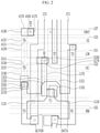
FIG. 1 is a circuit diagram of an embodiment of a display device. -
FIG. 2 is a top plan view of an embodiment of one pixel of the display device. -
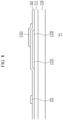
FIG. 3 is a cross-sectional view ofFIG. 2 , taken along line III-III. -
FIG. 4 shows a manufacturing an embodiment of sequence of each layer of the display device. -
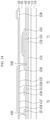
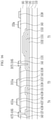
FIG. 5 to FIG. 18 are top plan or cross-sectional views that sequentially illustrate an embodiment of a manufacturing sequence of the display device. -
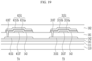
FIG. 19 is a cross-sectional view of an embodiment of a display device. -
FIG. 20 shows a manufacturing an embodiment of sequence of each layer of a display device. -
FIG. 21 to FIG. 25 are cross-sectional views that sequentially illustrate an embodiment of the manufacturing sequence of the display device. -
FIG. 26 is a top plan view of an embodiment of a pixel of a display device. -
FIG. 27 is a cross-sectional view ofFIG. 26 , taken along line XXVII-XXVII. - Hereinafter, the invention will be described more fully with reference to the accompanying drawings, in which embodiments of the invention are shown. As those skilled in the art would realize, the described embodiments may be modified in various different ways, all without departing from the scope of the claims.
- The drawings and description are to be regarded as illustrative in nature and not restrictive. Like reference numerals designate like elements throughout the specification.
- In addition, since the size and thickness of each component shown in the drawings are arbitrarily shown for better understanding and ease of description, the invention is not necessarily limited to what is shown. In the drawings, the thickness of layers, films, panels, regions, etc., are exaggerated for clarity. In addition, in the drawings, for better understanding and ease of description, the thickness of some layers and regions is exaggerated.
- It will be understood that when an element such as a layer, film, region, or substrate is referred to as being "on" another element, it can be directly on the other element or intervening elements may also be present. In contrast, when an element is referred to as being "directly on" another element, there are no intervening elements present. It will be understood that when an element such as a layer, film, region, or substrate is referred to as being "on" another element, it can be directly on the other element or intervening elements may also be present.
- In addition, unless explicitly described to the contrary, the word "comprise", and variations such as "comprises" or "comprising" will be understood to imply the inclusion of stated elements but not the exclusion of any other elements.
- It will be understood that, although the terms "first," "second," "third" etc. may be used herein to describe various elements, components, regions, layers and/or sections, these elements, components, regions, layers and/or sections should not be limited by these terms. These terms are only used to distinguish one element, component, region, layer or section from another element, component, region, layer or section. Thus, "a first element," "component," "region," "layer" or "section" discussed below could be termed a second element, component, region, layer or section without departing from the teachings herein.
- The terminology used herein is for the purpose of describing particular embodiments only and is not intended to be limiting. As used herein, the singular forms "a," "an," and "the" are intended to include the plural forms, including "at least one," unless the content clearly indicates otherwise. "Or" means "and/or." As used herein, the term "and/or" includes any and all combinations of one or more of the associated listed items. It will be further understood that the terms "comprises" and/or "comprising," or "includes" and/or "including" when used in this specification, specify the presence of stated features, regions, integers, steps, operations, elements, and/or components, but do not preclude the presence or addition of one or more other features, regions, integers, steps, operations, elements, components, and/or groups thereof.
- Furthermore, relative terms, such as "lower" or "bottom" and "upper" or "top," may be used herein to describe one element's relationship to another element as illustrated in the Figures. It will be understood that relative terms are intended to encompass different orientations of the device in addition to the orientation depicted in the Figures. In an embodiment, when the device in one of the figures is turned over, elements described as being on the "lower" side of other elements would then be oriented on "upper" sides of the other elements. The exemplary term "lower," can therefore, encompasses both an orientation of "lower" and "upper," depending on the particular orientation of the figure. Similarly, when the device in one of the figures is turned over, elements described as "below" or "beneath" other elements would then be oriented "above" the other elements. The exemplary terms "below" or "beneath" can, therefore, encompass both an orientation of above and below.
- "About" or "approximately" as used herein is inclusive of the stated value and means within an acceptable range of deviation for the particular value as determined by one of ordinary skill in the art, considering the measurement in question and the error associated with measurement of the particular quantity (i.e., the limitations of the measurement system). For example, "about" can mean within one or more standard deviations, or within ± 30%, 20%, 10%, 5% of the stated value.
- Unless otherwise defined, all terms (including technical and scientific terms) used herein have the same meaning as commonly understood by one of ordinary skill in the art to which this invention belongs. It will be further understood that terms, such as those defined in commonly used dictionaries, should be interpreted as having a meaning that is consistent with their meaning in the context of the relevant art and the invention, and will not be interpreted in an idealized or overly formal sense unless expressly so defined herein.
- Embodiments are described herein with reference to cross section illustrations that are schematic illustrations of idealized embodiments. As such, variations from the shapes of the illustrations as a result, for example, of manufacturing techniques and/or tolerances, are to be expected. Thus, embodiments described herein should not be construed as limited to the particular shapes of regions as illustrated herein but are to include deviations in shapes that result, for example, from manufacturing. In an embodiment, a region illustrated or described as flat may, typically, have rough and/or nonlinear features. Moreover, sharp angles that are illustrated may be rounded. Thus, the regions illustrated in the figures are schematic in nature and their shapes are not intended to illustrate the precise shape of a region and are not intended to limit the scope of the claims.
- First, referring to
FIG. 1 , a display device in an embodiment will be described. -
FIG. 1 is a circuit diagram of an embodiment of a display device. - As shown in
FIG. 1 , one pixel PX of a display device in an embodiment includes a plurality of transistors T1, T2, T3, T4, T5, T6, and T7 that are connected tomultiple wires - One pixel PX is connected with the plurality of
wires initialization voltage line 127, afirst scan line 151, asecond scan line 152, aninitialization control line 153, abypass control line 154, a lightemission control line 155, adata line 171, a drivingvoltage line 172, and acommon voltage line 741. - The
first scan line 151 is connected to a gate driver (not shown) and transmits a first scan signal GW to a second transistor T2. Thesecond scan line 152 may be applied with a voltage having a polarity opposite to a polarity of a voltage applied to thefirst scan line 151 at the same timing as that of a signal of thefirst scan line 151. In an embodiment, when a negative voltage is applied to thefirst scan line 151, a positive voltage may be applied to thesecond scan line 152, for example. Thesecond scan line 152 transmits a second scan signal GC to a third transistor T3. When describing the structure of transistors, especially in the claims and general part of the description, the third transistor T3 may be referred to as a second transistor. - The
initialization control line 153 transmits an initialization control signal GI to a fourth transistor T4. When describing the structure of transistors, especially in the claims and general part of the description, the fourth transistor T4 may be referred to as a third transistor. - The
bypass control line 154 transmits a bypass signal GB to a seventh transistor T7. Thebypass control line 154 may include a previous or nextfirst scan line 151. The lightemission control line 155 transmits a light emission control signal EM to a fifth transistor T5 and a sixth transistor T6. - The
data line 171 is a wire that transmits data voltage DATA generated from a data driver (not shown), and luminance of the light emitting diode LED changes according to the data voltage DATA applied to the pixel PX. - The driving
voltage line 172 applies a driving voltage ELVDD. Theinitialization voltage line 127 transmits an initialization voltage VINT. Thecommon voltage line 741 applies a common voltage ELVSS to a cathode of the light emitting diode LED. In the illustrated embodiment, a voltage applied to the drivingvoltage line 172, a voltage applied to theinitialization voltage line 127, and a voltage applied to thecommon voltage line 741 may be respectively constant voltages. - Hereinafter, the structure and connection relationship of the plurality of transistors will be described in detail.
- The driving transistor (also referred to as a first transistor) T1 may have a P-type transistor characteristic, and may include a polycrystalline semiconductor. The driving transistor T1 is a transistor that controls intensity of a current output to an anode of the light emitting diode LED according to the data voltage DATA applied to a gate electrode of the driving transistor T1. Since brightness of the light emitting diode LED is controlled according to intensity of a driving current output to the anode of the light emitting diode LED, luminance of the light emitting diode LED may be adjusted according to the data voltage DATA applied to the pixel PX. For this purpose, a first electrode of the driving transistor T1 is disposed to be able to receive the driving voltage ELVDD and thus is connected with the driving
voltage line 172 via the fifth transistor T5. A second electrode of the driving transistor T1 is disposed to be able to output a current toward the light emitting diode LED, and thus is connected with the anode of the light emitting diode LED via the sixth transistor T6. In addition, the second electrode of the driving transistor T1 is connected with a second electrode of the second transistor T2 and thus receives the data voltage DATA. In addition, the first electrode of the driving transistor T1 transmits the data voltage DATA applied to the second electrode to the third transistor T3. The gate electrode of the driving transistor T1 is connected with one electrode (hereinafter, referred to a second storage electrode) of the storage capacitor Cst. Thus, a voltage of the gate electrode of the driving transistor T1 is changed according to a voltage stored in the storage capacitor Cst, and accordingly, the driving current output from the driving transistor T1 is changed. In addition, the storage capacitor Cst also serves to maintain the voltage of the gate electrode of the driving transistor T1 at a constant level for one frame period. - The second transistor T2 may have a P-type transistor characteristic, and may include a polycrystalline semiconductor. The second transistor T2 is a transistor that receives the data voltage DATA into the pixel PX. A gate electrode of the second transistor T2 is connected with the
first scan line 151. A first electrode of the second transistor T2 is connected with thedata line 171. A second electrode of the second transistor T2 is connected with the second electrode of the driving transistor T1. When the second transistor T2 is turned on by a negative voltage among the first scan signal GW transmitted through thefirst scan line 151, the data voltage DATA transmitted through thedata line 171 is transmitted to the second electrode of the driving transistor T1. - The third transistor T3 may have an N-type transistor characteristic, and may include an oxide semiconductor. The third transistor T3 electrically connects the first electrode and the gate electrode of the driving transistor T1. Thus, the third transistor T3 is a transistor that enables a compensation voltage, which is the data voltage DATA that is changed through the driving transistor T1, to be transmitted to a second storage electrode of the storage capacitor Cst. A gate electrode of the third transistor T3 is connected with the
second scan line 152, and a first electrode of the third transistor T3 is connected with the first electrode of the driving transistor T1. A second electrode of the third transistor T3 is connected with the second storage electrode of the storage capacitor Cst and the gate electrode of the driving transistor T1. The third transistor T3 is turned on by the positive voltage of the second scan signal GC transmitted through thesecond scan line 152, connects the gate electrode of the driving transistor T1 and the first electrode of the driving transistor T1, and transmits a voltage applied to the gate electrode of the driving transistor T1 to the second storage electrode of the storage capacitor Cst such that the transmitted voltage is stored in the storage capacitor Cst. - The fourth transistor T4 may have an N-type transistor characteristic, and may include an oxide semiconductor. The fourth transistor T4 serves to initialize the gate electrode of the driving transistor T1 and the second storage electrode of the storage capacitor Cst. A gate electrode of the fourth transistor T4 is connected with the
initialization control line 153, and a first electrode of the fourth transistor T4 is connected with theinitialization voltage line 127. A second electrode of the fourth transistor T4 is connected to the second storage electrode of the storage capacitor Cst and the gate electrode of the driving transistor T1 via the second electrode of the third transistor T3. The fourth transistor T4 is turned on by the positive voltage of an initialization control signal GI transmitted through theinitialization control line 153, and thus transmits the initialization voltage VINT to the gate electrode of the driving transistor T1 and the second storage electrode of the storage capacitor Cst. Accordingly, the voltage of the gate electrode of the driving transistor T1 and the storage capacitor Cst is initialized. - The fifth transistor T5 may have a P-type transistor characteristic, and may include a polycrystalline semiconductor. The fifth transistor T5 serves to transmit the driving voltage ELVDD to the driving transistor T1. A gate electrode of the fifth transistor T5 is connected with the light
emission control line 155, a first electrode of the fifth transistor T5 is connected with the drivingvoltage line 172, and a second electrode of the fifth transistor T5 is connected with the first electrode of the driving transistor T1. - The sixth transistor T6 may have a P-type transistor characteristic, and may include a polycrystalline semiconductor. The sixth transistor T6 serves to transmit the driving current output from the driving transistor T1 to the light emitting diode LED. A gate electrode of the sixth transistor T6 is connected with the light
emission control line 155, a first electrode of the sixth transistor T6 is connected with the second electrode of the driving transistor T1, and a second electrode of the sixth transistor T6 is connected with the anode of the light emitting diode LED. - The seventh transistor T7 may have a P-type transistor characteristic, and may include a polycrystalline semiconductor. The seventh transistor T7 serves to initialize the anode of the light emitting diode LED. A gate electrode of the seventh transistor T7 is connected with the
bypass control line 154, a first electrode of the seventh transistor T7 is connected with the anode of the light emitting diode LED, and a second electrode of the seventh transistor T7 is connected with theinitialization voltage line 127. When the seventh transistor T7 is turned on by the negative voltage of the bypass signal GB, the initialization voltage VINT is applied to the anode of the light emitting diode LED and thus the anode of the light emitting diode LED is initialized. - In the above description, one pixel PX includes seven transistors T1 to T7 and one storage capacitor Cst, but this is not restrictive, and the number of transistors, the number of capacitors, and the connection relationship therebetween may be variously modified.
- In the illustrated embodiment, the driving transistor T1 may include a polycrystalline semiconductor. In addition, the third transistor T3 and the fourth transistor T4 may include an oxide semiconductor. The second transistor T2, the fifth transistor T5, the sixth transistor T6, and the seventh transistor T7 may include a polycrystalline semiconductor. However, this is not restrictive, and at least one or more of the second transistor T2, the fifth transistor T5, the sixth transistor T6, and the seventh transistor T7 may include an oxide semiconductor. In the illustrated embodiment, the third transistor T3 and the fourth transistor T4 include a semiconductor material that is different from that of the driving transistor T1 to thereby achieve stable driving and improve reliability.
- Hereinafter, planar and cross-sectional structures of the driving transistor T1, the third transistor T3, the fourth transistor T4, and the like will be described in detail with reference to
FIG. 2 to FIG. 18 . -
FIG. 2 is a top plan view of an embodiment of one pixel of the display device,FIG. 3 is a cross-sectional view ofFIG. 2 , taken along line III-III, andFIG. 4 shows an embodiment of a manufacturing sequence of each layer of the display device.FIG. 5 to FIG. 18 are top plan or cross-sectional views that sequentially illustrate an embodiment of a manufacturing sequence of the display device.FIG. 5 ,FIG. 7 ,FIG. 9 ,FIG. 11 ,FIG. 13 ,FIG. 15 , andFIG. 17 are top plan views, andFIG. 6 ,FIG. 8 ,FIG. 10 ,FIG. 12 ,FIG. 14 ,FIG. 16 , andFIG. 18 are cross-sectional views. Since the seventh transistor T7 is connected to afirst scan line 151 of the next stage, the seventh transistor T7 is not illustrated, and instead, a seventh transistor T7 of the previous stage is illustrated. - As shown in
FIG. 4 , a polycrystalline semiconductor ACT1 (LTPS), a first gate conductor GAT1, a second gate conductor GAT2, and an oxide semiconductor ACT2 (Oxide) are provided, and then an opening CNT1 may be defined in an insulation layer. Next, a third gate conductor GAT3 and a fourth gate conductor GAT4 are provided, and then an opening CNT2 may be defined. Subsequently, a data conductor SD may be provided. - As shown in
FIG. 2 to FIG. 18 , the polycrystalline semiconductor ACT1 (LTPS) that includes achannel 1132, afirst electrode 1131, and asecond electrode 1133 of the driving transistor T1 may be disposed on asubstrate 110.FIG. 5 andFIG. 6 illustrate the polycrystalline semiconductor polycrystalline semiconductor ACT1 (LTPS). The polycrystalline semiconductor ACT1 (LTPS) may further include channels, first electrodes, and second electrodes of the second transistor T2, the fifth transistor T5, the sixth transistor T6, and the seventh transistor T7 in addition to the driving transistor T1. - The
channel 1132 of the driving transistor T1 may have a shape that is bent in a plan view. However, the shape of thechannel 1132 of the driving transistor T1 is not limited thereto, and may be variously modified. In an embodiment, thechannel 1132 of the driving transistor T1 may be bent into other shapes, and for example, may be bent into a shape of a bar, for example. Thefirst electrode 1131 and thesecond electrode 1133 of the driving transistor T1 may be respectively disposed at opposite sides of thechannel 1132 of the driving transistor T1. Thefirst electrode 1131 of the driving transistor T1 extends downward in a plan view and thus may be connected with a second electrode of the fifth transistor T5. Thesecond electrode 1133 of the driving transistor T1 vertically extends in a plan view, and a portion extended upward may be connected with a second electrode of the second transistor T2 and a portion extended downward may be connected with a first electrode of the sixth transistor T6. - A
buffer layer 111 may be disposed between thesubstrate 110 and the polycrystalline semiconductor that includes thechannel 1132, thefirst electrode 1131, and thesecond electrode 1133 of the driving transistor T1. Thebuffer layer 111 may have a single layer or multi-layer structure. Thebuffer layer 111 may include an organic insulating material or an inorganic insulating material. - A first
gate insulation layer 141 may be disposed on the polycrystalline semiconductor that includes thechannel 1132, thefirst electrode 1131, and thesecond electrode 1133 of the driving transistor T1. The firstgate insulation layer 141 may include a silicon nitride, a silicon oxide, and the like. - A first gate conductor GAT1 that includes the
gate electrode 1151 of the driving transistor T1 may be disposed on the firstgate insulation layer 141.FIG. 7 andFIG. 8 illustrate the polycrystalline semiconductor ACT1 (LTPS) and the first gate conductor GAT1. The first gate conductor GAT1 may further include gate electrodes of the second transistor T2, the fifth transistor T5, the sixth transistor T6, and the seventh transistor T7 in addition to the driving transistor T1. - The
gate electrode 1151 of the driving transistor T1 may overlap thechannel 1132 of the driving transistor T1. Thechannel 1132 of the driving transistor T1 is covered by thegate electrode 1151 of the driving transistor T1. - The first gate conductor GAT1 may further include a
first scan line 151 and a lightemission control line 155. Thefirst scan line 151 and the lightemission control line 155 may extend approximately in a horizontal direction. Thefirst scan line 151 may be connected with a gate electrode of the second transistor T2. Thefirst scan line 151 may be unitary with the gate electrode of the second transistor T2. Thefirst scan line 151 may be connected with a gate electrode of the seventh transistor T7 that is disposed in a pixel of the previous stage. That is, a bypass control line connected to the seventh transistor T7 may include afirst scan line 151 of the next stage. Thefirst scan line 151 may be unitary with a gate electrode of the seventh transistor T7 that is disposed in the pixel of the previous stage. A gate electrode of the fifth transistor T5 and a gate electrode of the sixth transistor T6 may be connected with the lightemission control line 155. The gate electrode of the fifth transistor T5 and the gate electrode of the sixth transistor T6 may be unitary with the lightemission control line 155. - After forming the first gate conductor GAT1 that includes the
gate electrode 1151 of the driving transistor T1, a doping process or a plasma process may be performed. A portion of the polycrystalline semiconductor ACT1 (LTPS), covered by the first gate conductor GAT1, does not experience the doping or plasma treatment, and a portion of the polycrystalline semiconductor ACT1 (LTPS), not covered by the first gate conductor GAT1, experiences doping or plasma treatment, thereby having the same characteristic as that of a conductor. In this case, a P-type dopant may be used, and the driving transistor T1, the second transistor T2, the fifth transistor T5, the sixth transistor T6, and the seventh transistor T7 that include the polycrystalline semiconductor ACT1 (LTPS) may have P-type transistor characteristics. - A second
gate insulation layer 142 may be disposed on the first gate conductor GAT1 that includes thegate electrode 1151 of the driving transistor T1, and the firstgate insulation layer 141. The secondgate insulation layer 142 may include a silicon nitride, a silicon oxide, and the like. - A second gate conductor GAT2 that includes a
first storage electrode 1153 of the storage capacitor Cst may be disposed on the secondgate insulation layer 142.FIG. 9 andFIG. 10 illustrate the polycrystalline semiconductor ACT1 (LTPS), the first gate conductor GAT1, and the second gate conductor GAT2. - The
first storage electrode 1153 forms the storage capacitor Cst by overlapping thegate electrode 1151 of the driving transistor T1. Anopening 1152 is defined in thefirst storage electrode 1153 of the storage capacitor Cst. Theopening 1152 of thefirst storage electrode 1153 of the storage capacitor Cst may overlap thegate electrode 1151 of the driving transistor T1. - The second gate conductor GAT2 may further include an
initialization voltage line 127. Theinitialization voltage line 127 may extend approximately in a horizontal direction. - A first
interlayer insulation layer 161 may be disposed on the second gate conductor that includes thefirst storage electrode 1153 of the storage capacitor Cst. The firstinterlayer insulation layer 161 may include a silicon nitride, a silicon oxide, and the like. - An oxide semiconductor ACT2 (Oxide) that includes a
channel 3137, afirst electrode 3136, and asecond electrode 3138 of the third transistor T3, and achannel 4137, afirst electrode 4136, and asecond electrode 4138 of the fourth transistor T4, may be disposed on the firstinterlayer insulation layer 161.FIG. 11 andFIG. 12 illustrate the polycrystalline semiconductor ACT1 (LTPS), the first gate conductor GAT1, the second gate conductor GAT2, and the oxide semiconductor ACT2 (Oxide). - In an embodiment, the oxide semiconductor may include at least one of unary metal oxides such as indium oxide (In), tin oxide (Sn), zinc oxide (Zn), and the like, binary metal oxides such as In-Zn oxide, Sn-Zn oxide, Al-Zn oxide, Zn-Mg oxide, Sn-Mg oxide, In-Mg oxide, In-Ga oxide, and the like, ternary metal oxides such as In-Ga-Zn oxide, In-Al-Zn oxide, In-Sn-Zn oxide, Sn-Ga-Zn oxide, Al-Ga-Zn oxide, Sn-Al-Zn oxide, In- Hf-Zn oxide, In-La-Zn oxide, In-Ce-Zn oxide, In-Pr-Zn oxide, In-Nd-Zn oxide, In-Sm-Zn oxide, In-Eu- Zn oxide, In-Gd-Zn oxide, In-Tb-Zn oxide, In-Dy-Zn oxide, In-Ho-Zn oxide, In-Er-Zn oxide, In-Tm-Zn oxide, In-Yb-Zn oxide, In-Lu-Zn oxide, and the like, and quaternary metal oxides such as In-Sn-Ga-Zn oxide, In-Hf-Ga-Zn oxide, In-Al-Ga-Zn oxide, In-Sn-Al-Zn oxide, In-Sn-Hf-Zn oxide, In-Hf-Al-Zn oxide, and the like. In an embodiment, the oxide semiconductor may include indium-gallium-zinc oxide ("IGZO") among the In-Ga-Zn-based oxides, for example.
- The
channel 3137, thefirst electrode 3136, and thesecond electrode 3138 of the third transistor T3, and thechannel 4137, thefirst electrode 4136, and thesecond electrode 4138 of the fourth transistor T4, may be connected with each other and thus may be unitary with each other. Thefirst electrode 3136 and thesecond electrode 3138 of the third transistor T3 may be respectively disposed at opposite sides of thechannel 3137 of the third transistor T3. Thefirst electrode 4136 and thesecond electrode 4138 of the fourth transistor T4 may be respectively disposed at opposite sides of thechannel 4137 of the fourth transistor T4. Thesecond electrode 3138 of the third transistor T3 may be connected with thesecond electrode 4138 of the fourth transistor T4. - A third
gate insulation layer 143 may be disposed on the semiconductor oxide that includes thechannel 3137, thefirst electrode 3136, and thesecond electrode 3138 of the third transistor T3 and thechannel 4137, thefirst electrode 4136, and thesecond electrode 4138 of the fourth transistor T4. The thirdgate insulation layer 143 may overlap thechannel 3137 of the third transistor T3, and may not overlap thefirst electrode 3136 and thesecond electrode 3138 of the third transistor T3. In addition, the thirdgate insulation layer 143 may overlap thechannel 4137 of the fourth transistor T4, and may not overlap thefirst electrode 4136 and thesecond electrode 4138 of the fourth transistor T4. - A third gate conductor GAT3 that includes a
lower gate electrode 3151a of the third transistor T3 and alower gate electrode 4151a of the fourth transistor T4 may be disposed on the thirdgate insulation layer 143.FIG. 15 andFIG. 16 illustrates the polycrystalline semiconductor ACT1 (LTPS), the first gate conductor GAT1, the second gate conductor GAT2, the oxide semiconductor ACT2 (Oxide), and the third gate conductor GAT3. In addition,FIG. 15 andFIG. 16 illustrate an opening CNT1 defined in the thirdgate insulation layer 143. - The
lower gate electrode 3151a of the third transistor T3 may overlap thechannel 3137 of the third transistor T3. Thelower gate electrode 4151a of the fourth transistor T4 may overlap thechannel 4137 of the fourth transistor T4. - The third gate conductor GAT3 may further include a lower
second scan line 152a and a lowerinitialization control line 153a. The lowersecond scan line 152a and the lowerinitialization control line 153a may extend approximately in a horizontal direction. The lowersecond scan line 152a may be connected with thelower gate electrode 3151a of the third transistor T3. The lowersecond scan line 152a may be unitary with thelower gate electrode 3151a of the third transistor T3. The lowerinitialization control line 153a may be connected with thelower gate electrode 4151a of the fourth transistor T4. The lowerinitialization control line 153a may be unitary with thelower gate electrode 4151a of the fourth transistor T4. - The third gate conductor GAT3 may further include a lower first connection electrode 3175 (which also may be termed as a first connection electrode 3175) and a lower second connection electrode 4175 (which also may be termed as a third connection electrode 4175). The lower
first connection electrode 3175 may overlap thefirst electrode 1131 of the driving transistor T1. The lowerfirst connection electrode 3175 may be disposed to be adjacent to thefirst electrode 3136 of the third transistor T3. The lowersecond connection electrode 4175 may overlap theinitialization voltage line 127. The lowersecond connection electrode 4175 may be disposed to be adjacent to thefirst electrode 4136 of the fourth transistor T4. - The first
gate insulation layer 141, the secondgate insulation layer 142, and the firstinterlayer insulation layer 161 may be disposed on an entirety of thesubstrate 110. The thirdgate insulation layer 143 is not disposed on an entirety of thesubstrate 110, but may be disposed only in some regions. The thirdgate insulation layer 143 may be disposed only under the third gate conductor. The thirdgate insulation layer 143 may be disposed between thelower gate electrode 3151a of the third transistor T3 and thechannel 3137 of the third transistor T3. The thirdgate insulation layer 143 is not disposed on thefirst electrode 3136 and thesecond electrode 3138 of the third transistor T3. The thirdgate insulation layer 143 may be disposed between thelower gate electrode 4151a of the fourth transistor T4 and thechannel 4137 of the fourth transistor T4. The thirdgate insulation layer 143 is not disposed on thefirst electrode 4136 and thesecond electrode 4138 of the fourth transistor T4. The thirdgate insulation layer 143 may be disposed between the lowersecond scan line 152a and the lowerinitialization control line 153a. The thirdgate insulation layer 143 may be disposed between the lowerfirst connection electrode 3175 and the lowersecond connection electrode 4175. - A
first opening 3165 and asecond opening 4165 may be defined in the thirdgate insulation layer 143. Thefirst opening 3165 may overlap thefirst electrode 1131 of the driving transistor T1. Thefirst opening 3165 may overlap the lowerfirst connection electrode 3175. Thefirst opening 3165 may be further defined in the firstinterlayer insulation layer 161, the secondgate insulation layer 142, and the firstgate insulation layer 141. The lowerfirst connection electrode 3175 may be connected with thefirst electrode 1131 of the driving transistor T1 through thefirst opening 3165. Thesecond opening 4165 may overlap theinitialization voltage line 127. Thesecond opening 4165 may overlap the lowersecond connection electrode 4175. Thesecond opening 4165 may be further defined in the firstinterlayer insulation layer 161. The lowersecond connection electrode 4175 may be connected with theinitialization voltage line 127 through asecond opening 4165. - After forming the third gate conductor GAT3 that includes the
lower gate electrode 3151a of the third transistor T3 and thelower gate electrode 4151a of the fourth transistor T4, a doping process or plasma treatment may be performed. A portion of the oxide semiconductor ACT2 (Oxide), covered by the third gate conductor GAT3 does not experience the doping process or plasma treatment, and a portion of the oxide semiconductor ACT2 (Oxide), not covered by the third gate conductor GAT3 may be doped or plasma-treated, thereby having the same characteristic as that of a conductor. Thechannel 3137 of the third transistor T3 may be disposed below thegate electrode 3151 to thereby overlap thegate electrode 3151. Thefirst electrode 3136 and thesecond electrode 3138 of the third transistor T3 may not overlap thegate electrode 3151. Thechannel 4137 of the fourth transistor T4 may be disposed below thegate electrode 4151 to as to overlap thegate electrode 4151. Thefirst electrode 4136 and thesecond electrode 4138 of the fourth transistor T4 may not overlap thegate electrode 4151. In this case, an N-type dopant may be used, and the third transistor T3 and the fourth transistor T4 including an oxide semiconductor material may have an N-type transistor characteristic. - A fourth gate conductor GAT4 that includes an
upper gate electrode 3151b of the third transistor T3 and anupper gate electrode 4151b of the fourth transistor T4 may be disposed on the third gate conductor GAT3.FIG. 17 andFIG. 18 illustrate the polycrystalline semiconductor ACT1 (LTPS), the first gate conductor GAT1, the second gate conductor GAT2, the oxide semiconductor ACT2 (Oxide), the opening CNT1, the third gate conductor GAT3, and the fourth gate conductor GAT4. - The fourth gate conductor GAT4 may be disposed above the third gate conductor GAT3. An insulation layer is not disposed between the third gate conductor GAT3 and the fourth gate conductor GAT4. The third gate conductor GAT3 and the fourth gate conductor GAT4 may contact each other.
- The
upper gate electrode 3151b of the third transistor T3 may be disposed on thelower gate electrode 3151a of the third transistor T3. Theupper gate electrode 3151b of the third transistor T3 may be disposed above thelower gate electrode 3151a of the third transistor T3. Theupper gate electrode 3151b of the third transistor T3 may contact thelower gate electrode 3151a of the third transistor T3. Theupper gate electrode 3151b of the third transistor T3 may have the same shape as that of thelower gate electrode 3151a of the third transistor T3 in a plan view. - The
upper gate electrode 4151b of the fourth transistor T4 may be disposed above thelower gate electrode 4151a of the fourth transistor T4. Theupper gate electrode 4151b of the fourth transistor T4 may be directly disposed above thelower gate electrode 4151a of the fourth transistor T4. Theupper gate electrode 4151b of the fourth transistor T4 may contact thelower gate electrode 4151a of the fourth transistor T4. Theupper gate electrode 4151b of the fourth transistor T4 may have the same shape as that of thelower gate electrode 4151a of the fourth transistor T4 in a plan view. - The fourth gate conductor may further include an upper
second scan line 152b and an upperinitialization control line 153b. The uppersecond scan line 152b and the upperinitialization control line 153b may extend approximately in a horizontal direction. The uppersecond scan line 152b may be disposed above the lowersecond scan line 152a. The uppersecond scan line 152b may be disposed directly above the lowersecond scan line 152a. The uppersecond scan line 152b and the lowersecond scan line 152a may contact each other. The uppersecond scan line 152b may have the same shape as that of the lowersecond scan line 152a in a plan view. The uppersecond scan line 152b may be connected with theupper gate electrode 3151b of the third transistor T3. The uppersecond scan line 152b may be unitary with theupper gate electrode 3151b of the third transistor T3. The upperinitialization control line 153b may be disposed on the lowerinitialization control line 153a. The upperinitialization control line 153b may be disposed directly above the lowerinitialization control line 153a. The upperinitialization control line 153b and the lowerinitialization control line 153a may contact each other. The upperinitialization control line 153b may have the same shape as that of the lowerinitialization control line 153a in a plan view. The upperinitialization control line 153b may be connected with theupper gate electrode 4151b of the fourth transistor T4. The upperinitialization control line 153b may be unitary with theupper gate electrode 4151b of the fourth transistor T4. - The fourth gate conductor may further include an upper first connection electrode 3176 (which also may be termed as a second connection electrode 3176) and an upper second connection electrode 4176 (which also may be termed as a fourth connection electrode 4176). The upper
first connection electrode 3176 may overlap thefirst electrode 1131 of the driving transistor T1, the lowerfirst connection electrode 3175, and thefirst electrode 3136 of the third transistor T3. The upperfirst connection electrode 3176 may be disposed directly above the lowerfirst connection electrode 3175 and thefirst electrode 3136 of the third transistor T3. The upperfirst connection electrode 3176 and the lowerfirst connection electrode 3175 may contact each other, and the upperfirst connection electrode 3176 and thefirst electrode 3136 of the third transistor T3 may contact each other. The upperfirst connection electrode 3176 may electrically connect thefirst electrode 1131 of the driving transistor T1 and thefirst electrode 3136 of the third transistor T3. The uppersecond connection electrode 4176 may overlap theinitialization voltage line 127, the lowersecond connection electrode 4175, and thefirst electrode 4136 of the fourth transistor T4. The uppersecond connection electrode 4176 may be disposed directly above the lowersecond connection electrode 4175 and thefirst electrode 4136 of the fourth transistor T4. The uppersecond connection electrode 4176 and the lowersecond connection electrode 4175 may contact each other, and the uppersecond connection electrode 4176 and thefirst electrode 4136 of the fourth transistor T4 may contact each other. The uppersecond connection electrode 4176 may electrically connect theinitialization voltage line 127 and thefirst electrode 4136 of the fourth transistor T4. - The fourth gate conductor may further include a
protection pad 3178. Theprotection pad 3178 may be disposed on thesecond electrode 3138 of the third transistor T3. Theprotection pad 3178 may be disposed directly on thesecond electrode 3138 of the third transistor T3. Theprotection pad 3178 and thesecond electrode 3138 of the third transistor T3 may contact each other. Theprotection pad 3178 may be disposed to cover the top surface and the side surface of thesecond electrode 3138 of the third transistor T3. - A second
interlayer insulation layer 162 may be disposed on the fourth gate conductor GAT4 that includes theupper gate electrode 3151b of the third transistor T3 and theupper gate electrode 4151b of the fourth transistor T4. Athird opening 3166 may be defined in the secondinterlayer insulation layer 162. Thethird opening 3166 may overlap theprotection pad 3178 and thesecond electrode 3138 of the third transistor T3. - A data conductor SD that includes a
third connection electrode 1175 may be disposed on the secondinterlayer insulation layer 162. - The
third connection electrode 1175 may overlap theprotection pad 3178 and thesecond electrode 3138 of the third transistor T3. Thethird connection electrode 1175 may be connected with theprotection pad 3178 through thethird opening 3166. Thethird connection electrode 1175 may be connected with thesecond electrode 3138 of the third transistor T3 through theprotection pad 3178. Thethird connection electrode 1175 may overlap thegate electrode 1151 of the driving transistor T1. Thethird connection electrode 1175 may be connected with thegate electrode 1151 of the driving transistor T1. Thethird connection electrode 1175 may electrically connect thesecond electrode 3138 of the third transistor T3 and thegate electrode 1151 of the driving transistor T1. - The data conductor SD may further include the
data line 171 and the drivingvoltage line 172. Thedata line 171 and the drivingvoltage line 172 may extend approximately in a vertical direction. Thedata line 171 may be connected with the second transistor T2. The drivingvoltage line 172 may be connected with the fifth transistor T5. In addition, the drivingvoltage line 172 may be connected with thefirst storage electrode 1153. - In the above description, the
third connection electrode 1175, thedata line 171, and the drivingvoltage line 172 are disposed in the same layer, and thus form the data conductor SD, but the invention is not limited thereto, and various modifications are available. In an embodiment, the data conductor SD may include the first data conductor and the second data conductor, for example. In this case, an insulation layer may be disposed between the first data conductor and the second data conductor. Some of thethird connection electrode 1175, thedata line 171, and the drivingvoltage line 172 may be included in the first data conductor, and a part of the other may be included in the second data conductor. - Although it is not illustrated, a protective film may be disposed on the data conductor SD, and an anode may be disposed on the protective film. The anode may be connected with the sixth transistor T6, and may receive an output current of the driving transistor T1. A partitioning wall may be disposed on the anode. An opening is defined in the partitioning wall, and the opening of the partitioning wall may overlap the anode. A light emission element layer may be disposed in the opening of the partitioning wall. A cathode may be disposed on the light emission element layer and the partitioning wall. The anode, the light emission element layer, and the cathode may form a light emitting diode LED.
- Next, referring to
FIG. 1 to FIG. 18 , a method for manufacturing a display device in an embodiment will be described. - First, as shown in
FIG. 5 andFIG. 6 , abuffer layer 111 may be provided by an organic insulation material or an inorganic insulation material on asubstrate 110. Thebuffer layer 111 may be disposed on an entirety of thesubstrate 110. Thebuffer layer 111 may have a single or multi-layer structure. Thebuffer layer 111 may be omitted depending on cases. - Subsequently, a polycrystalline semiconductor ACT1 (LTPS) may be provided by a polycrystalline semiconductor material on the
buffer layer 111. Achannel 1132, afirst electrode 1131, and asecond electrode 1133 of a driving transistor T1 may be provided by patterning the polycrystalline semiconductor ACT1 (LTPS) through a photo and etching process. In this case, channels, first electrodes, and second electrodes of a second transistor T2, a fifth transistor T5, a sixth transistor T6, and a seventh transistor T7 may be further provided in addition to the driving transistor T1. - As shown in
FIG. 7 andFIG. 8 , a firstgate insulation layer 141 may be provided by a silicon nitride, a silicon oxide, and the like, on the polycrystalline semiconductor ACT1 (LTPS). The firstgate insulation layer 141 may be disposed on an entirety of thesubstrate 110. - Subsequently, a first gate conductor GAT1 may be provided by a metallic material on the first
gate insulation layer 141. The first gate conductor GAT1 is patterned through a photo and etching process such that agate electrode 1151 of the driving transistor T1 may be disposed. In this case, gate electrodes of the second transistor T2, the fifth transistor T5, the sixth transistor T6, and the seventh transistor T7 may be further provided in addition to the gate electrode of the driving transistor T1. In addition, afirst scan line 151 and a lightemission control line 155 may be provided. - The
gate electrode 1151 of the driving transistor T1 may be patterned to overlap thechannel 1132 of the driving transistor T1. In this case, thegate electrode 1151 of the driving transistor T1 may be patterned so that it does not overlap with thefirst electrode 1131 and thesecond electrode 1133 of the driving transistor T1. Thefirst scan line 151 may be patterned to be connected to the gate electrode of the second transistor T2. The lightemission control line 155 may be patterned to be connected to the gate electrode of the fifth transistor T5 and the gate electrode of the sixth transistor T6. - After patterning the first gate conductor GAT1, a doping or plasma treatment is performed to adjust electrical conductivity of the polycrystalline semiconductor ACT1 (LTPS). When a doping process or a plasma treatment is performed on an entirety of the
substrate 110, a portion of the polycrystalline semiconductor ACT1 (LTPS) covered by the first gate conductor GAT1 is not doped or plasma-treated, and a portion of the polycrystalline semiconductor ACT1 (LTPS) not covered by the first gate conductor GAT1 is doped or plasma-treated and thus may have the same characteristic as that of a conductor. Thus, thefirst electrode 1131 and thesecond electrode 1133 of the driving transistor T1 may have the same characteristic as that of a conductor. In this case, a P-type dopant may be used, and the driving transistor T1, the second transistor T2, the fifth transistor T5, the sixth transistor T6, and the seventh transistor T7 that include a polycrystalline semiconductor material may have a P-type transistor characteristic. - As shown in
FIG. 9 andFIG. 10 , a secondgate insulation layer 142 may be provided by a silicon nitride, a silicon oxide, and the like on the first gate conductor GAT1 and the firstgate insulation layer 141. In this case, the secondgate insulation layer 142 may be disposed on an entirety of thesubstrate 110. - Subsequently, a second gate conductor GAT2 may be provided by a metallic material on the second
gate insulation layer 142. Afirst storage electrode 1153 of the storage capacitor Cst may be provided by patterning the second gate conductor GAT2 through a photo and etching process. In this case, aninitialization voltage line 127 may be further provided. - The
first storage electrode 1153 of the storage capacitor Cst forms the storage capacitor Cst by overlapping thegate electrode 1151 of the driving transistor T1. Theinitialization voltage line 127 may extend approximately in a horizontal direction. - As shown in
FIG. 11 andFIG. 12 , a firstinterlayer insulation layer 161 may be provided by a silicon nitride, a silicon oxide, and the like on the second gate conductor GAT2 and the secondgate insulation layer 142. In this case, the firstinterlayer insulation layer 161 may be disposed on an entirety of thesubstrate 110. - Subsequently, an oxide semiconductor ACT2 (Oxide) may be provided by an oxide semiconductor material on the first
interlayer insulation layer 161. Achannel 3137, afirst electrode 3136, and asecond electrode 3138 of the third transistor T3 and achannel 4137, afirst electrode 4136, and asecond electrode 4138 of the fourth transistor T4 may be provided by patterning the oxide semiconductor ACT2(Oxide) through a photo and etching process. - The
channel 3137, thefirst electrode 3136, and thesecond electrode 3138 of the third transistor T3 and thechannel 4137, thefirst electrode 4136, and thesecond electrode 4138 of the fourth transistor T4 may be connected with each other and thus may be unitary. - As shown in
FIG. 13 andFIG. 14 , a thirdgate insulation layer 143 may be provided by a silicon nitride, a silicon oxide, and the like on the oxide semiconductor ACT2 (Oxide) and the firstinterlayer insulation layer 161. In this case, the thirdgate insulation layer 143 may be disposed on an entirety of thesubstrate 110. - Subsequently, an opening CNT1 may be defined by patterning the third
gate insulation layer 143 through a photo and etching process. In this case, a firstinterlayer insulation layer 161, a secondgate insulation layer 142, and a firstgate insulation layer 141, which are disposed below the thirdgate insulation layer 143, may also be patterned together. Afirst opening 3165 and asecond opening 4165 may be defined in the thirdgate insulation layer 143. Thefirst opening 3165 may be defined in the thirdgate insulation layer 143, the firstinterlayer insulation layer 161, the secondgate insulation layer 142, and the firstgate insulation layer 141. At least a part of the top surface of thefirst electrode 1131 of the driving transistor T1 may be exposed to the outside by thefirst opening 3165. That is, thefirst opening 3165 may overlap at least a part of thefirst electrode 1131 of the driving transistor T1. Thesecond opening 4165 may be defined in the thirdgate insulation layer 143 and the firstinterlayer insulation layer 161. At least a part of the top surface of theinitialization voltage line 127 may be exposed to the outside by thesecond opening 4165. That is, thesecond opening 4165 may overlap at least a part of theinitialization voltage line 127. - While an etching process for defining the
first opening 3165 and thesecond opening 4165 is carried out, thechannel 3137, thefirst electrode 3136, and thesecond electrode 3138 of the third transistor T3 and thechannel 4137, thefirst electrode 4136, and thesecond electrode 4138 of the fourth transistor T4, which include an oxide semiconductor material, are covered by the thirdgate insulation layer 143. Thus, thechannel 3137, thefirst electrode 3136, and thesecond electrode 3138 of the third transistor T3 and thechannel 4137, thefirst electrode 4136, and thesecond electrode 4138 of the fourth transistor T4 may be prevented from being damaged due to the etching process. - As shown in
FIG. 15 andFIG. 16 , a third gate conductor GAT3 may be disposed on the thirdgate insulation layer 143 by a metallic material. Alower gate electrode 3151a of the third transistor T3 and alower gate electrode 4151a of the fourth transistor T4 may be provided by patterning the third gate conductor GAT3 through a photo and etching process. In this case, a lowersecond scan line 152a and a lowerinitialization control line 153a may be further provided. In addition, a lowerfirst connection electrode 3175 and a lowersecond connection electrode 4175 may be further provided. - The
lower gate electrode 3151a of the third transistor T3 may overlap thechannel 3137 of the third transistor T3. Thelower gate electrode 4151a of the fourth transistor T4 may overlap thechannel 4137 of the fourth transistor T4. The lowersecond scan line 152a and the lowerinitialization control line 153a may extend approximately in a horizontal direction. The lowersecond scan line 152a may be connected with thelower gate electrode 3151a of the third transistor T3. The lowerinitialization control line 153a may be connected with thelower gate electrode 4151a of the fourth transistor T4. The lowerfirst connection electrode 3175 may be connected with thefirst electrode 1131 of the driving transistor T1 through thefirst opening 3165. The lowersecond connection electrode 4175 may be connected with theinitialization voltage line 127 through thesecond opening 4165. - Subsequently, the third
gate insulation layer 143 may be patterned through an etching process using the third gate conductor GAT3 as a mask. A portion of the thirdgate insulation layer 143, covered by the third gate conductor GAT3, remains, and a portion of the thirdgate insulation layer 143, not covered by the third gate conductor GAT3, is removed. Thus, portions of the thirdgate insulation layer 143, disposed below thelower gate electrode 3151a of the third transistor T3, thelower gate electrode 4151a of the fourth transistor T4, the lowersecond scan line 152a, the lowerinitialization control line 153a, the lowerfirst connection electrode 3175, and the lowersecond connection electrode 4175, remain. Portions of the thirdgate insulation layer 143, disposed above thefirst electrode 3136 and thesecond electrode 3138 of the third transistor T3 and thefirst electrode 4136 and thesecond electrode 4138 of the fourth transistor T4 are removed. - After patterning the third gate conductor GAT3, a doping or plasma treatment is performed such that electrical conductivity of the oxide semiconductor ACT2 (Oxide) may be adjusted. When the doping process or the plasma treatment is performed throughout the
substrate 110, a portion of the oxide semiconductor ACT2 (Oxide) covered by the third gate conductor GAT3 is not doped or plasma-treated, and a portion of the oxide semiconductor ACT2 (Oxide) not covered by the third gate conductor GAT3 is doped or plasma-treated such that the portion has the same characteristic as that of a conductor. Thus, thefirst electrode 3136 and thesecond electrode 3138 of the third transistor T3 and thefirst electrode 4136 and thesecond electrode 4138 of the fourth transistor T4 may have the same characteristic as that of a conductor. In this case, an N-type dopant may be used, and the third transistor T3 and the fourth transistor T4 that include the oxide semiconductor material may have an N-type transistor characteristic. - As shown in
FIG. 17 andFIG. 18 , a fourth gate conductor GAT4 may be disposed on the third gate conductor GAT3, the oxide semiconductor ACT2 (Oxide), and the firstinterlayer insulation layer 161 by a metallic material. The fourth gate conductor GAT4 is disposed directly above the third gate conductor GAT3, the oxide semiconductor ACT2 (Oxide) and the firstinterlayer insulation layer 161. Thus, the fourth gate conductor GAT4 may contact the third gate conductor GAT3, and the fourth gate conductor GAT4 may contact the oxide semiconductor ACT2 (Oxide). The fourth gate conductor GAT4 is patterned through a photo and etching process and thus theupper gate electrode 3151b of the third transistor T3 and theupper gate electrode 4151b of the fourth transistor T4 may be provided. In this case, an uppersecond scan line 152b and an upperinitialization control line 153b may be further provided. In addition, an upperfirst connection electrode 3176, an uppersecond connection electrode 4176, and aprotection pad 3178 may be further provided. - The
upper gate electrode 3151b of the third transistor T3 may be disposed on thelower gate electrode 3151a of the third transistor T3. Theupper gate electrode 3151b of the third transistor T3 may have the same shape as that of thelower gate electrode 3151a of the third transistor T3 in a plan view. Theupper gate electrode 4151b of the fourth transistor T4 may be disposed on thelower gate electrode 4151a of the fourth transistor T4. Theupper gate electrode 4151b of the fourth transistor T4 may have the same shape as that of thelower gate electrode 4151a of the fourth transistor T4. - The upper
second scan line 152b and the upperinitialization control line 153b may extend approximately in a horizontal direction. The uppersecond scan line 152b may be disposed on the lowersecond scan line 152a, and may be connected with theupper gate electrode 3151b of the third transistor T3. The uppersecond scan line 152b may have the same shape as that of the lowersecond scan line 152a in a plan view. The upperinitialization control line 153b may be disposed on the lowerinitialization control line 153a, and may be connected with theupper gate electrode 4151b of the fourth transistor T4. The upperinitialization control line 153b may have the same shape as that of the lowerinitialization control line 153a in a plan view. - The upper
first connection electrode 3176 may be disposed on the lowerfirst connection electrode 3175 and thefirst electrode 3136 of the third transistor T3. The upperfirst connection electrode 3176 may electrically connect thefirst electrode 1131 of the driving transistor T1 with thefirst electrode 3136 of the third transistor T3. In this case, the upperfirst connection electrode 3176 and thefirst electrode 1131 of the driving transistor T1 may be connected through the lowerfirst connection electrode 3175, and the lowerfirst connection electrode 3175 may be connected with thefirst electrode 1131 of the driving transistor T1 through thefirst opening 3165. In addition, the upperfirst connection electrode 3176 may be directly connected with thefirst electrode 3136 of the third transistor T3. - The upper
second connection electrode 4176 may be disposed on the lowersecond connection electrode 4175 and thefirst electrode 4136 of the fourth transistor T4. The uppersecond connection electrode 4176 may electrically connect theinitialization voltage line 127 and thefirst electrode 4136 of the fourth transistor T4. In this case, the uppersecond connection electrode 4176 and theinitialization voltage line 127 may be connected through the lowersecond connection electrode 4175, and the lowersecond connection electrode 4175 may be connected with theinitialization voltage line 127 through thesecond opening 4165. In addition, the uppersecond connection electrode 4176 may be directly connected with thefirst electrode 4136 of the fourth transistor T4. - When a transistor including a polycrystalline semiconductor material and a transistor that includes an oxide semiconductor material are connected through a connection electrode, one opening is defined for connection with the connection electrode and the transistor including the polycrystalline semiconductor material, and another opening may be further defined for connection with the connection electrode and the transistor including the oxide semiconductor material. In this case, by increasing the number of openings, the distance between the electrodes may increase, and accordingly, the size of each pixel may increase. In the illustrated embodiment, one opening connects the connection electrode and the transistor including the polycrystalline semiconductor material, and the connection electrode and the transistor including an oxide semiconductor material are directly connected, thereby reducing the number of openings. Accordingly, a distance between electrodes may be reduced, the size of each pixel may be reduced, and a high resolution display device may be implemented.
- In addition, in the illustrated embodiment, the third gate conductor GAT3 is provided first and then the fourth gate conductor GAT4 is disposed thereon and thus the
first electrode 3136 and thesecond electrode 3138 of the third transistor T3 and thefirst electrode 4136 and thesecond electrode 4138 of the fourth transistor T4 may be prevented from being damaged. As a comparative example, when the third gate conductor GAT3 and the fourth gate conductor GAT4 are unitary with one pattern, a process for defining the opening CNT1 and a process for exposing a part of the oxide semiconductor ACT2 (Oxide) may be simultaneously performed. In this case, the oxide semiconductor ACT2 (Oxide) may be damaged due to an etching solution used to form the opening CNT1. In the illustrated embodiment, a process for defining the opening CNT1 and a process for exposing a part of the oxide semiconductor ACT2 (Oxide) are separately performed, thereby preventing the oxide semiconductor ACT2 (Oxide) from being damaged. In this case, the third gate conductor GAT3 and the fourth gate conductor GAT4 may include the same metallic material, or may include different metallic materials. - The
protection pad 3178 may be disposed on thesecond electrode 3138 of the third transistor T3. Theprotection pad 3178 may serve to protect thesecond electrode 3138 of the third transistor T3 in a subsequent process. - As shown in
FIG. 2 andFIG. 3 , the secondinterlayer insulation layer 162 may be disposed on the fourth gate conductor GAT4, the oxide semiconductor ACT2 (Oxide), and the firstinterlayer insulation layer 161 by a silicon nitride, a silicon oxide, and the like. In this case, the secondinterlayer insulation layer 162 may be disposed on an entirety of thesubstrate 110. The secondinterlayer insulation layer 162 may not be in contact with the upper surface of the thirdgate insulation layer 143. The secondinterlayer insulation layer 162 may contact the side surface of the thirdgate insulation layer 143. - Subsequently, the second
interlayer insulation layer 162 is patterned to form an opening CNT2 through a photo and etching process. Athird opening 3166 may be defined in the secondinterlayer insulation layer 162. At least part of the top surface of theprotection pad 3178 may be exposed to the outside by thethird opening 3166. That is, thethird opening 3166 may at least partially overlap theprotection pad 3178. - In this case, a buffered oxide etchant ("BOE") may be used. The BOE is a chemical combination of ammonium fluoride (NH4F) and hydrofluoric acid ("HF"), and may be used in etching of silicon dioxide. During etching, hydrogen fluoride is directly involved in oxide etching, and ammonium fluoride may be act as a buffer solution that improves uniformity by adjusting the etching ratio. The BOE may be used in cleaning processes, such as removing organic materials from the upper surface of the substrate, and may be a part of a metal etching solution. When the oxide semiconductor is exposed in the process of defining the opening CNT2, the oxide semiconductor may be damaged by the BOE. In the illustrated embodiment, since the
protection pad 3178 is disposed on thesecond electrode 3138 of the third transistor T3 including the oxide semiconductor material, damage to thesecond electrode 3138 of the third transistor T3 may be prevented in the process of defining thethird opening 3166. - Subsequently, the data conductor SD may be disposed on the second
interlayer insulation layer 162 by a metallic material. Thethird connection electrode 1175 may be provided by patterning the data conductor SD through a photo and etching process. In this case, thedata line 171 and the drivingvoltage line 172 may be further provided. - The
third connection electrode 1175 may be connected to theprotection pad 3178 through thethird opening 3166. Thethird connection electrode 1175 may be connected to thesecond electrode 3138 of the third transistor T3 through theprotection pad 3178. Thethird connection electrode 1175 may be connected to thegate electrode 1151 of the driving transistor T1. Thethird connection electrode 1175 may be electrically connected to thesecond electrode 3138 of the third transistor T3 and thegate electrode 1151 of the driving transistor T1. Thedata line 171 and the drivingvoltage line 172 may extend approximately in a vertical direction. - In the above description, an operation for forming the data conductor SD on the second
interlayer insulation layer 162 is described, but the invention is not limited thereto, and various modifications are available. In an embodiment, the first data conductor may be disposed on the secondinterlayer insulation layer 162 and then patterned, an insulation layer may be disposed on the first data conductor, and the second data conductor may be disposed on the insulation layer and then patterned, for example. In this case, a part of thethird connection electrode 1175, thedata line 171, and the drivingvoltage line 172 may be included in the first data conductor, and a part of the rest may be included in the second data conductor. - Although it is not illustrated, a protective layer may be disposed on the data conductor SD and the second
interlayer insulation layer 162. An anode may be disposed on the protective layer by a metal or a metallic oxide. The anode may be connected with the sixth transistor T6, and may receive an output current of the driving transistor T1. A partitioning wall may be disposed on the anode and the protective layer. An opening may expose the anode by patterning the partitioning wall, and a light emission element layer may be disposed in the opening of the partitioning wall. A cathode may be disposed on the light emission element layer and the partitioning wall. The anode, the light emission element layer, and the cathode may form a light emitting diode LED. - Next, referring to
FIG. 19 , a display device in an embodiment will be described. - A display device in an embodiment shown in
FIG. 19 is substantially the same as the display device in the embodiment shown inFIG. 1 to FIG. 18 , and therefore, description of the same parts will be omitted. Unlike the previously described embodiment, in the embodiment, third and fourth transistors include dual gate electrodes, and this difference will be described in detail hereinafter. -
FIG. 19 is a cross-sectional view of an embodiment of a display device.FIG. 19 shows a partial region of a third transistor and a fourth transistor. - As in the above-described embodiment, a pixel PX of a display device in the illustrated embodiment includes a plurality of transistors T1, T2, T3, T4, T5, T6, and T7 connected to a plurality of wires, a storage capacitor Cst, and a light emitting diode LED.
- Among the plurality of transistors, a third transistor T3 may include a
channel 3137, afirst electrode 3136, asecond electrode 3138, alower gate electrode 3151a, and anupper gate electrode 3151b. In the illustrated embodiment, the third transistor T3 may further include alight blocking layer 3155. Thelight blocking layer 3155 of the third transistor T3 may overlap thechannel 3137, and a gate electrode 3135 of the third transistor T3. A voltage applied to thegate electrode 3151 may be the same as a voltage applied to thelight blocking layer 3155. Thus, the third transistor may include a dual gate electrode. In this case, thegate electrode 3151 may be connected with thelight blocking layer 3155. An opening 3167 (which may be termed as a light blocking layer connecting opening 3167) that overlaps thegate electrode 3151 and thelight blocking layer 3155 may be defined in the thirdgate insulation layer 143. Thelower gate electrode 3151 may be connected with thelight blocking layer 3155 through theopening 3167. - The fourth transistor T4 may include a
channel 4137, afirst electrode 4136, asecond electrode 4138, alower gate electrode 4151a, and anupper gate electrode 4151b. In the illustrated embodiment, the fourth transistor T4 may further include alight blocking layer 4155. Thelight blocking layer 4155 of the fourth transistor T4 may overlap thechannel 4137 and agate electrode 4151 of the fourth transistor T4. A voltage applied to thegate electrode 4151 may be the same as a voltage applied to thelight blocking layer 4155. Thus, the fourth transistor T4 may include a dual gate electrode. In this case, thegate electrode 4151 may be connected with thelight blocking layer 4155. Anopening 4167 that overlaps thegate electrode 4151 and thelight blocking layer 4155 may be defined in the thirdgate insulation layer 143. Thelower gate electrode 4151 may be connected with thelight blocking layer 4155 through theopening 4167. - As a comparative example, when a gate electrode and a light blocking layer are connected through a connection electrode, an opening connects the gate electrode and the connection electrode, and another opening may connect the light blocking layer and the connection electrode. In this case, by increasing the number of openings, the distance between the electrodes may increase, and accordingly, the size of each pixel may increase. In the illustrated embodiment, one opening directly connects the gate electrode and the light blocking layer, thereby reducing the number of openings. Accordingly, a distance between electrodes may be reduced, the size of each pixel may be reduced, and a high resolution display device may be implemented.
- Next, a display device in an embodiment and a method for manufacturing the display device will be described with reference to
FIG. 20 to FIG. 25 . - A display device in an embodiment of
FIG. 20 to FIG. 25 is substantially the same as the display device in the embodiment ofFIG. 1 to FIG. 18 , and therefore, the same portions will not be described. The illustrated embodiment is different from the above-described embodiment in that a second gate conductor and an oxide semiconductor are unitary, and this will be described in detail hereinafter. -
FIG. 20 shows a manufacturing an embodiment of sequence of each layer of a display device.FIG. 21 to FIG. 25 are cross-sectional views that sequentially illustrate an embodiment of the manufacturing sequence of the display device. - As shown in
FIG. 20 , a polycrystalline semiconductor ACT1 (LTPS), a first gate conductor GAT1, and an oxide semiconductor ACT2 (Oxide) are provided, and then an opening CNT1 may be defined in an insulation layer. Subsequently, a third gate conductor GAT3 and a fourth gate conductor GAT4 are provided, and then an opening CNT2 may be defined. Subsequently, a data conductor SD may be provided. In the above-described embodiment, the second gate conductor GAT2 is provided before forming the oxide semiconductor ACT2 (Oxide), and in the illustrated embodiment, the second gate conductor GAT2 is omitted. Wires included in the second gate conductor GAT2 in the above-described embodiment may be included in the oxide semiconductor ACT2 (Oxide). - As shown in
FIG. 21 , as in the above-described embodiment, abuffer layer 111 is disposed on asubstrate 110, and a polycrystalline semiconductor ACT1 (LTPS) may be disposed on thebuffer layer 111. Achannel 1132, afirst electrode 1131, and asecond electrode 1133 of a driving transistor T1 may be provided by patterning the polycrystalline semiconductor ACT1 (LTPS). A firstgate insulation layer 141 may be disposed on the polycrystalline semiconductor ACT1 (LTPS). - Subsequently, a first gate conductor GAT1 may be disposed on the first
gate insulation layer 141. Agate electrode 1151, afirst scan line 151, and the driving transistor T1 may be provided by patterning the first gate conductor GAT1. In this case, aninitialization voltage line 127 may be further provided. Theinitialization voltage line 127 is included in the second gate conductor GAT2 in the above-described embodiment, and theinitialization voltage line 127 may be included in the first gate conductor GAT1 in the illustrated embodiment. After patterning the first gate conductor GAT1, a doping process or a plasma treatment may be carried out. - As shown in
FIG. 22 , a secondgate insulation layer 142 may be disposed on the first gate conductor GAT1 and the firstgate insulation layer 141. - Subsequently, an oxide semiconductor ACT2 (Oxide) may be disposed on the second
gate insulation layer 142. Achannel 3137, afirst electrode 3136, and asecond electrode 3138 of a third transistor T3 and achannel 4137, afirst electrode 4136, and asecond electrode 4138 of a fourth transistor T4 may be provided by patterning the oxide semiconductor ACT2 (Oxide). In this case, afirst storage electrode 1153 may be further provided. - As shown in
FIG. 23 , a thirdgate insulation layer 143 may be disposed on an oxide semiconductor ACT2 (Oxide) and a secondgate insulation layer 142. Subsequently, an opening CNT1 may be defined by patterning the thirdgate insulation layer 143. Afirst opening 3165 and asecond opening 4165 may be defined in the thirdgate insulation layer 143. Thefirst opening 3165 may be defined in the thirdgate insulation layer 143, the secondgate insulation layer 142, and the firstgate insulation layer 141. Thefirst opening 3165 may overlap at least a part of thefirst electrode 1131 of the driving transistor T1. Thesecond opening 4165 may be defined in the thirdgate insulation layer 143 and the secondgate insulation layer 142. Thesecond opening 4165 may overlap at least a part of theinitialization voltage line 127. - While an etching process for defining the
first opening 3165 and thesecond opening 4165 is being carried out, thechannel 3137, thefirst electrode 3136, and thesecond electrode 3138 of the third transistor T3 and thechannel 4137, thefirst electrode 4136, and thesecond electrode 4138 of the fourth transistor T4 that include an oxide semiconductor material are covered by the thirdgate insulation layer 143. Thus, thechannel 3137, thefirst electrode 3136, and thesecond electrode 3138 of the third transistor T3 and thechannel 4137, thefirst electrode 4136, and thesecond electrode 4138 of the fourth transistor T4 may be prevented from being damaged due to the etching process. - Subsequently, a third gate conductor GAT3 may be disposed on the third
gate insulation layer 143. Alower gate electrode 3151a of the third transistor T3, alower gate electrode 4151a of the fourth transistor T4, a lowersecond scan line 152a, a lowerfirst connection electrode 3175, a lowersecond connection electrode 4175, and the like may be provided by patterning the third gate conductor GAT3. The thirdgate insulation layer 143 may be patterned through an etching process by the third gate conductor GAT3 as a mask. A portion of the thirdgate insulation layer 143 that is covered by the third gate conductor GAT3 remains, and a portion of the thirdgate insulation layer 143 not covered by the third gate conductor GAT3 is removed. - After patterning the third gate conductor GAT3, a doping process or a plasma treatment may be carried out. The
first electrode 3136 and thesecond electrode 3138 of the third transistor T3 and thefirst electrode 4136 and thesecond electrode 4138 of the fourth transistor T4 may have the same characteristic as that of a conductor. In addition, afirst storage electrode 1153 has the same characteristic as that of a conductor. - As shown in
FIG. 24 , a fourth gate conductor GAT4 may be disposed on the third gate conductor GAT3, the oxide semiconductor ACT2 (Oxide), and the secondgate insulation layer 142. The fourth gate conductor GAT4 is disposed directly above the third gate conductor GAT3, the oxide semiconductor ACT2 (Oxide), and the secondgate insulation layer 142. Thus, the fourth gate conductor GAT4 may contact the third gate conductor GAT3, and the fourth gate conductor GAT4 may contact the oxide semiconductor ACT2 (Oxide). Anupper gate electrode 3151b of the third transistor T3, anupper gate electrode 4151b of the fourth transistor T4, an uppersecond scan line 152b, an upperfirst connection electrode 3176, an uppersecond connection electrode 4176, and aprotection pad 3178 may be provided by patterning the fourth gate conductor GAT4. - The upper
first connection electrode 3176 may electrically connect thefirst electrode 1131 of the driving transistor T1 and thefirst electrode 3136 of the third transistor T3. The uppersecond connection electrode 4176 may electrically connect theinitialization voltage line 127 with thefirst electrode 4136 of the fourth transistor T4. - In the illustrated embodiment, one opening connects a connection electrode and a transistor including a polycrystalline semiconductor material, and the connection electrode and the transistor that includes the oxide semiconductor material are directly connected, thereby reducing the number of openings. Accordingly, a distance between electrodes may be reduced, the size of each pixel may be reduced, and a high resolution display device may be implemented.
- In the illustrated embodiment, a process for defining the opening CNT1 and a process for exposing a part of the oxide semiconductor ACT2 (Oxide) are separately performed, thereby preventing the oxide semiconductor ACT2 (Oxide) from being damaged. In this case, the third gate conductor GAT3 and the fourth gate conductor GAT4 may include the same metallic material, or may include different metallic materials.
- As shown in
FIG. 25 , a secondinterlayer insulation layer 162 may be disposed on the fourth gate conductor GAT4, the oxide semiconductor ACT2 (Oxide), and the secondgate insulation layer 142. The secondinterlayer insulation layer 162 may not contact the top surface of the thirdgate insulation layer 143. The secondinterlayer insulation layer 162 may contact the side surface of the thirdgate insulation layer 143. - Subsequently, an opening CNT2 may be defined by patterning the second
interlayer insulation layer 162. Athird opening 3166 may be defined in the secondinterlayer insulation layer 162. Thethird opening 3166 may overlap at least a part of theprotection pad 3178. - In this case, a BOE may be used. In the illustrated embodiment, the
protection pad 3178 is disposed on thesecond electrode 3138 of the third transistor T3 that includes an oxide semiconductor material, and thus thesecond electrode 3138 of the third transistor T3 may be prevented from being damaged during a process for defining thethird opening 3166. - Subsequently, a data conductor SD may be disposed on the second
interlayer insulation layer 162. Athird connection electrode 1175, adata line 171, and a drivingvoltage line 172 may be provided by patterning the data conductor SD. Thethird connection electrode 1175 may electrically connect thesecond electrode 3138 of the third transistor T3 and thegate electrode 1151 of the driving transistor T1. - In the above-description, an operation for forming the data conductor SD on the second
interlayer insulation layer 162 has been described, but the invention is not limited thereto, and various modifications are possible. In an embodiment, a first data conductor is disposed on the secondinterlayer insulation layer 162 and then patterned, an insulation layer is disposed on the first data conductor, and a second data conductor is disposed on the insulation layer and then patterned, for example. In this case, some of thethird connection electrode 1175, thedata line 171, and the drivingvoltage line 172 may be included in the first data conductor, and some of the rest may be included in the second data conductor. - Although it is not illustrated, a protection layer may be disposed on the data conductor SD and the second
interlayer insulation layer 162. An anode may be disposed on the protection layer by a metal or a metallic oxide. The anode may be connected with a sixth transistor T6, and may receive an output current of the driving transistor T1. A partitioning wall may be disposed on the anode and the protection layer. An opening exposes the anode by patterning the partitioning wall, and a light emission element layer may be disposed in the opening of the partitioning wall. A cathode may be disposed on the light emission element layer and the partitioning wall. The anode, the light emission element layer, and the cathode may form a light emitting diode LED. - Next, a display device in an embodiment and a method for manufacturing the same will be described with reference to
FIG. 26 andFIG. 27 . - A display device in an embodiment shown in
FIG. 26 andFIG. 27 is substantially the same as the display device in the embodiment shown inFIG. 1 to FIG. 18 , and therefore the same portions will not be described. The illustrated embodiment is different from the above-described embodiment in that an upper first connection electrode does not overlap a part of a lower first connection electrode, and an upper second connection electrode does not overlap a part of a lower second connection electrode, and this will be described hereinafter in detail. -
FIG. 26 is a top plan view of a pixel of a display device in an embodiment, andFIG. 27 is a cross-sectional view ofFIG. 26 , taken along line XXVII-XXVII. - As in the above-described embodiment, in a pixel of a display device in the illustrated embodiment includes a plurality of transistors T1, T2, T3, T4, T5, T6, and T7 connected to a plurality of
wires - In the above-described embodiment, an upper
first connection electrode 3176 may overlap an entirety of the lowerfirst connection electrode 3175. That is, the upperfirst connection electrode 3176 may cover an entirety of the top surface of the lowerfirst connection electrode 3175. In addition, the uppersecond connection electrode 4176 may overlap an entirety of the lowersecond connection electrode 4175. That is, the uppersecond connection electrode 4176 may cover an entirety of the top surface of the lowersecond connection electrode 4175. - In the illustrated embodiment, as shown in
FIG. 26 andFIG. 27 , the upperfirst connection electrode 3176 may overlap a part of the lowerfirst connection electrode 3175, and may not overlap a part of the rest. That is, the upperfirst connection electrode 3176 may cover a part of the top surface of the lowerfirst connection electrode 3175. Thus, a part of the top surface of the lowerfirst connection electrode 3175 may not be covered by the upperfirst connection electrode 3176. The area and position where the upperfirst connection electrode 3176 overlaps the lowerfirst connection electrode 3175 may be variously changed. In addition, the uppersecond connection electrode 4176 may overlap a part of the lowersecond connection electrode 4175 and may not overlap a part of the rest. That is, the uppersecond connection electrode 4176 may cover a part of the top surface of the lowersecond connection electrode 4175. Therefore, a part of the top surface of the lowersecond connection electrode 4175 may not be covered by the uppersecond connection electrode 4176. The area and position where the uppersecond connection electrode 4176 overlaps the lowersecond connection electrode 4175 may be changed in various ways. - Similarly, the
upper gate electrode 3151b of the third transistor T3 overlaps an entirety of thelower gate electrode 3151a, but this is not restrictive, and may be various modified. Theupper gate electrode 3151b of the third transistor T3 may overlap a part of thelower gate electrode 3151a. In addition, theupper gate electrode 3151b of the third transistor T3 may cover the top and side surfaces of thelower gate electrode 3151a. Further, theupper gate electrode 4151b of the fourth transistor T4 is illustrated to overlap an entirety of thelower gate electrode 4151a, but is not limited thereto and may be variously changed. Theupper gate electrode 4151b of the fourth transistor T4 may overlap a part of thelower gate electrode 4151a. In addition, theupper gate electrode 4151b of the fourth transistor T4 may cover the top and side surfaces of thelower gate electrode 4151a. - While this invention has been described in connection with what is presently considered to be practical embodiments, it is to be understood that the invention is not limited to the disclosed embodiments. On the contrary, it is intended to cover various modifications and equivalent arrangements included within the scope of the appended claims.
Claims (22)
- A display device comprising:a substrate (110);a first transistor (T1) comprising:a channel (1132) which is disposed on the substrate (110);a first electrode (1131) and a second electrode (1132) respectively disposed at opposite sides of the channel (1132) of the first transistor (T1); anda gate electrode (1151) overlapping the channel (1132) of the first transistor (T1);a first interlayer insulation layer (161) which is disposed on the first electrode (1131), the second electrode (1132) and/or the gate electrode (1151) of the first transistor (T1);a second transistor (T3) comprising:a channel (3137) which is disposed on the first interlayer insulation layer (161);a first electrode (3136) and a second electrode (3138) respectively disposed at opposite sides of the channel (3137) of the second transistor (T3); anda gate electrode (3151) which overlaps the channel (3137) of the second transistor (T3);a first connection electrode (3175) which is disposed on the first interlayer insulation layer (161), and connected with the first electrode (1131) of the first transistor (T1);a gate insulation layer (143) which is disposed between the first interlayer insulation layer (161) and the first connection electrode (3175); anda second connection electrode (3176) which connects the first connection electrode (3175) and the first electrode (3136) of the second transistor (T3).
- The display device of claim 1, wherein the second connection electrode (3176) is disposed directly above the first connection electrode (3175), and the second connection electrode (3176) and the first connection electrode (3175) contact each other.
- The display device of claim 1 or 2, wherein the second connection electrode (3176) is disposed directly above the first electrode (3136) of the second transistor (T3), and the second connection electrode (3176) and the first electrode (3136) of the second transistor (T3) contact each other.
- The display device of at least one of claims 1 to 3, wherein a first opening (3165) which overlaps at least a part of the first electrode (1131) of the first transistor (T1) is defined in the first interlayer insulation (161) and the gate insulation layer (143), and
the first connection electrode (3175) is connected with the first electrode (1131) of the first transistor (T1) through the first opening (3165). - The display device of at least one of claims 1 to 4, wherein a planar shape of the first connection electrode (3175) is the same as a planar shape of the gate insulation layer (143).
- The display device of at least one of claims 1 to 5, wherein the gate electrode (3151) of the second transistor (T3) comprises a first gate electrode (3151a) and a second gate electrode (3151b),the gate insulation layer (143) is further disposed between the first gate electrode (3151a) of the second transistor (T3) and the channel (3137) of the second transistor (T3),the first connection electrode (3175) is disposed in a same layer as the first gate electrode (3151a) of the second transistor (T3), andthe second connection electrode (3176) is disposed in a same layer as the second gate electrode (3151b) of the second transistor (T3).
- The display device of at least one of claims 1 to 6, wherein the channel (1132), the first electrode (1131), and the second electrode (1132) of the first transistor (T1) comprise a polycrystalline semiconductor material, and
the channel (3137), the first electrode (3136), and the second electrode (3138) of the second transistor (T3) comprise an oxide semiconductor material. - The display device of at least one of claims 1 to 7, further comprising:an initialization voltage line (127) which is disposed on the substrate (110);a third transistor (T4) comprising:a channel (4137) disposed on the first interlayer insulation layer (161);a first electrode (4136) and a second electrode (4138) of the third transistor (T4), respectively disposed at opposite sides of the channel (4137) of the third transistor (T4); anda gate electrode (4151) overlapping the channel (4137) of the third transistor (T4);a third connection electrode (4175) which is connected to the initialization voltage line (127); anda fourth connection electrode (4176) which is disposed directly above the third connection electrode (4175) and the first electrode (4136) of the third transistor (T4),wherein the first interlayer insulation layer (161) and the gate insulation layer (143) are further disposed between the initialization voltage line (127) and the third connection electrode (4175),a second opening (4165) which overlaps the initialization voltage line (127) is defined in the first interlayer insulation layer (161) and the gate insulation layer (143),the third connection electrode (4175) is connected with the initialization voltage line (127) through the second opening (4165), andthe second electrode (4138) of the third transistor (T4) and the second electrode (3138) of the second transistor (T3) are connected to each other.
- The display device of at least one of claims 1 to 8, further comprising a protection pad (3178) which is disposed on the second electrode (3138) of the second transistor (T3),
wherein the protection pad (3178) is disposed in a same layer as the second connection electrode (3176). - The display device of claim 9, further comprising:a second interlayer insulation layer (162) which is disposed on the protection pad (3178); anda third connection electrode (4175) which is disposed on the second interlayer insulation layer (162), and connects the gate electrode (1151) of the first transistor (T1) and the protection pad (3178),wherein a third opening (3166) which overlaps the protection pad (3178) is defined in the second interlayer insulation layer (162), andthe third connection electrode (4175) is connected with the protection pad (3178) through the third opening (3166).
- The display device of at least one of claims 1 to 10, further comprising a light blocking layer (3155) which overlaps the channel (3137) and the gate electrode (3151) of the second transistor (T3),wherein the first interlayer insulation layer (161) and the gate insulation layer (143) are further disposed between the light blocking layer (3155) and the gate electrode (3151) of the second transistor (T3),a light blocking layer connecting opening (3167) which overlaps the light blocking layer (3155) is defined in the first interlayer insulation layer (161) and the gate insulation layer (143), andthe gate electrode (3151) of the second transistor (T3) is connected with the light blocking layer (3155) through the light blocking layer connecting opening (3167) .
- The display device of at least one of claims 1 to 11, further comprising a first storage electrode (1153) which overlaps the gate electrode (1151) of the first transistor (T1),
wherein the first storage electrode (1153) includes a same material as a material of the channel (3137), the first electrode (3136), and the second electrode (3138) of the second transistor (T3), and is disposed in a same layer as the channel (3137), the first electrode (3136), and the second electrode (3138) of the second transistor (T3). - A manufacturing method of a display device, the display device especially according to at least one of claims 1 to 12, the method comprising:forming a channel (1132) of a first transistor (T1) on a substrate (110), and a first electrode (1132) and a second electrode (1132) respectively disposed at opposite sides of the channel (1132);forming a gate electrode (1151) of the first transistor (T1), overlapping the channel (1132) of the first transistor (T1);forming a first interlayer insulation layer (161) on the gate electrode (1151) of the first transistor (T1);forming a channel (3137) of a second transistor (T3) on the first interlayer insulation layer (161), and a first electrode (3136) and a second electrode (3138) which are respectively disposed at opposite sides of the channel (3137) of the second transistor (T3);forming a gate insulation layer (143) on the channel (3137), the first electrode (3136), and the second electrode (3138) of the second transistor (T3), and the first interlayer insulation layer (161);defining a first opening (3165) which overlaps the first electrode (1131) of the first transistor (T1) in the gate insulation layer (143) and the first interlayer insulation layer (161);forming a first connection electrode (3175) which is connected with the first electrode (1131) of the first transistor (T1) through the first opening (3165) on the gate insulation layer (143);removing a portion of the gate insulation layer (143), disposed on the first electrode (3136) of the second transistor (T3) by etching the gate insulation layer (143) using the first connection electrode (3175) as a mask; andforming a second connection electrode (3176) which connects the first connection electrode (3175) and the first electrode (3136) of the second transistor (T3).
- The manufacturing method of the display device of claim 13, wherein, in the forming the first connection electrode (3175), a first gate electrode (3151a) of the second transistor (T3) overlaps the channel (3137) of the second transistor (T3),in the forming the second connection electrode (3176),a second gate electrode (3151b) of the second transistor (T3) overlaps the channel (3137) of the second transistor (T3).
- The manufacturing method of the display device of claim 14, wherein the second gate electrode (3151b) of the second transistor (T3) is disposed directly above the first gate electrode (3151a) of the second transistor (T3), and the second gate electrode (3151b) of the second transistor (T3) and the first gate electrode (3151a) of the second transistor (T3) contact each other.
- The manufacturing method of the display device of at least one of claims 13 to 15, further comprising forming an initialization voltage line (127) on the substrate (110),wherein in the forming the channel (3137), the first electrode (3136), and the second electrode (3138) of the second transistor (T3), a channel (4137) of a third transistor (T4), disposed on the first interlayer insulation layer (161), and a first electrode (4136) and a second electrode (4138) which are respectively disposed at opposite sides of the channel (4137) of the third transistor (T4) are formed,in the defining the first opening (3165), a second opening (4165) which overlaps the initialization voltage line (127) is formed in the gate insulation layer (143) and the first interlayer insulation layer (161),in the forming the first connection electrode (3175), a third connection electrode (4175) which is connected with the initialization voltage line (127) through the second opening (4165) is formed,in the removing of the portion of the gate insulation layer (143), disposed on the first electrode (3136) of the second transistor (T3), a portion of the gate insulation layer (143), disposed on the first electrode (4136) of the third transistor (T4) is removed by etching the gate insulation layer (143) using the third connection electrode (4175) as a mask, andforming a fourth connection electrode (4176) which connects the third connection electrode (4175) and the initialization voltage line (127) in the forming the second connection electrode (3176).
- The manufacturing method of the display device of claim 16, wherein the fourth connection electrode (4176) is disposed directly above the third connection electrode (4175), and the fourth connection electrode (4176) and the third connection electrode (4175) contact each other.
- The manufacturing method of the display device of claim 17, wherein the fourth connection electrode (4176) is disposed directly above the first electrode (4136) of the third transistor (T4), and the fourth connection electrode (4176) and the first electrode (4136) of the third transistor (T4) contact each other.
- The manufacturing method of the display device of at least one of claims 13 to 18, wherein, in the forming the second connection electrode (3176), a protection pad (3178) is formed on the second electrode (3138) of the second transistor (T3).
- The manufacturing method of the display device of claim 19, further comprising:forming a second interlayer insulation layer (162) on the protection pad (3178);defining a third opening (3166) which overlaps the protection pad (3178) in the second interlayer insulation layer (162); andforming a third connection electrode (4175) which is connected with the protection pad (3178) through the third opening (3166) on the second interlayer insulation layer (162),wherein the third connection electrode (4175) connects the gate electrode (1151) of the first transistor (T1) and the protection pad (3178).
- The manufacturing method of the display device of at least one of claims 13 to 20, further comprising forming a light blocking layer (3155) which overlaps the channel (3137) and the gate electrode (3151) of the second transistor (T3),a light blocking layer connecting opening (3167) which overlaps the light blocking layer (3155) is defined in the defining the first opening (3165),a first gate electrode (3151a) of the second transistor (T3), connected with the light blocking layer (3155) through the light blocking layer connecting opening (3167), is formed in the forming the first connection electrode (3175), anda second gate electrode (3151b) of the second transistor (T3) is formed on the first gate electrode (3151a) of the second transistor (T3) in the forming the second connection electrode (3176).
- The manufacturing method of the display device of at least one of claims 13 to 21, wherein a first storage electrode (1153) which overlaps the gate electrode (1151) of the first transistor (T1) is formed in the forming the channel (3137), the first electrode (3136), and the second electrode (3138) of the second transistor (T3).
Applications Claiming Priority (1)
| Application Number | Priority Date | Filing Date | Title |
|---|---|---|---|
| KR1020200099934A KR20220019880A (en) | 2020-08-10 | 2020-08-10 | Display device and method for manufacturing threrof |
Publications (2)
| Publication Number | Publication Date |
|---|---|
| EP3955299A2 true EP3955299A2 (en) | 2022-02-16 |
| EP3955299A3 EP3955299A3 (en) | 2022-08-03 |
Family
ID=77520484
Family Applications (1)
| Application Number | Title | Priority Date | Filing Date |
|---|---|---|---|
| EP21190242.4A Pending EP3955299A3 (en) | 2020-08-10 | 2021-08-09 | Display device and method for manufacturing thereof |
Country Status (4)
| Country | Link |
|---|---|
| US (1) | US11825703B2 (en) |
| EP (1) | EP3955299A3 (en) |
| KR (1) | KR20220019880A (en) |
| CN (1) | CN114078882A (en) |
Family Cites Families (20)
| Publication number | Priority date | Publication date | Assignee | Title |
|---|---|---|---|---|
| KR20070072207A (en) | 2005-12-31 | 2007-07-04 | 엘지.필립스 엘시디 주식회사 | Liquid crystal display device using poly-silicon tft and fabrication method thereof |
| US10020354B2 (en) | 2015-04-17 | 2018-07-10 | Apple Inc. | Organic light-emitting diode displays with silicon and semiconducting oxide thin-film transistors |
| KR102424108B1 (en) | 2015-11-26 | 2022-07-25 | 엘지디스플레이 주식회사 | Thin Film Transistor Substrate And Display Using The Same |
| KR102583770B1 (en) | 2016-09-12 | 2023-10-06 | 삼성디스플레이 주식회사 | Memory transistor and display apparatus having the same |
| JP2018074076A (en) | 2016-11-02 | 2018-05-10 | 株式会社ジャパンディスプレイ | Display device |
| JP6706570B2 (en) * | 2016-12-05 | 2020-06-10 | 株式会社Joled | Semiconductor device, method of manufacturing semiconductor device, and display device |
| JP2018170324A (en) * | 2017-03-29 | 2018-11-01 | 株式会社ジャパンディスプレイ | Display device |
| KR102305442B1 (en) | 2017-03-30 | 2021-09-28 | 삼성디스플레이 주식회사 | Pixel and organic light emitting display device having the same |
| US10797123B2 (en) | 2017-10-13 | 2020-10-06 | Samsung Display Co., Ltd. | Display panel and method of fabricating the same |
| KR102649752B1 (en) * | 2017-12-22 | 2024-03-19 | 엘지디스플레이 주식회사 | Display apparatus |
| KR102637791B1 (en) | 2018-02-13 | 2024-02-19 | 삼성디스플레이 주식회사 | Display apparatus |
| CN108288621B (en) | 2018-03-09 | 2021-01-26 | 京东方科技集团股份有限公司 | Manufacturing method of array substrate, array substrate and display panel |
| KR102652448B1 (en) | 2018-03-13 | 2024-03-29 | 삼성디스플레이 주식회사 | Display apparatus |
| KR102538000B1 (en) | 2018-03-29 | 2023-05-31 | 삼성디스플레이 주식회사 | Display apparatus |
| KR102591811B1 (en) | 2018-05-18 | 2023-10-23 | 삼성디스플레이 주식회사 | Thin film transistor substrate, method of manufacturing the same, and display device including the same |
| KR102577900B1 (en) * | 2018-06-12 | 2023-09-13 | 삼성디스플레이 주식회사 | Organic light emitting diode display device |
| US10818697B2 (en) | 2018-08-06 | 2020-10-27 | Sharp Kabushiki Kaisha | Semiconductor device, display device, and method of producing semiconductor device |
| KR20200023573A (en) | 2018-08-23 | 2020-03-05 | 삼성디스플레이 주식회사 | Display device and method for manufacturing the same |
| KR102426708B1 (en) | 2018-09-07 | 2022-07-29 | 삼성디스플레이 주식회사 | Display apparatus |
| KR20200048910A (en) * | 2018-10-31 | 2020-05-08 | 엘지디스플레이 주식회사 | Display device comprising a plurality of thin film trnasistors and method for manufacturing the same |
-
2020
- 2020-08-10 KR KR1020200099934A patent/KR20220019880A/en unknown
-
2021
- 2021-04-28 US US17/242,303 patent/US11825703B2/en active Active
- 2021-08-09 CN CN202110908698.7A patent/CN114078882A/en active Pending
- 2021-08-09 EP EP21190242.4A patent/EP3955299A3/en active Pending
Also Published As
| Publication number | Publication date |
|---|---|
| US11825703B2 (en) | 2023-11-21 |
| EP3955299A3 (en) | 2022-08-03 |
| US20220045147A1 (en) | 2022-02-10 |
| CN114078882A (en) | 2022-02-22 |
| KR20220019880A (en) | 2022-02-18 |
Similar Documents
| Publication | Publication Date | Title |
|---|---|---|
| US11751434B2 (en) | Semiconductor device including an oxide thin film transistor | |
| US11871596B2 (en) | Display device and method of manufacturing the same | |
| US10490617B2 (en) | Organic light emitting display device and a method of manufacturing the same | |
| US20210257431A1 (en) | Organic light emitting display apparatus and method of manufacturing the same | |
| US11908924B2 (en) | Semiconductor device including two thin-film transistors and method of fabricating the same | |
| KR102081283B1 (en) | Thin film semiconductor device, organic light emitting display, and method of manufacturing the same | |
| EP4329458A1 (en) | Organic light emitting diode display | |
| US8896044B1 (en) | Organic light emitting diode display | |
| US9502488B2 (en) | Organic light emitting diode display device and manufacturing method thereof | |
| CN110010058B (en) | Array substrate and display panel | |
| EP2991117A1 (en) | Organic light emitting diode display device and manufacturing method thereof | |
| KR102469793B1 (en) | Display device | |
| US7129524B2 (en) | Organic electroluminescent device and method for fabricating the same | |
| US20220181419A1 (en) | Display substrate, manufacturing method thereof and display device | |
| KR102568776B1 (en) | Organic light emitting display device | |
| EP3955299A2 (en) | Display device and method for manufacturing thereof | |
| KR102317835B1 (en) | Thin Film Transistor Array Substrate and Organic Light Emitting Diode Display Device Having The Same | |
| EP3937241A1 (en) | Display device and manufacturing method thereof | |
| US11751443B2 (en) | Organic light emitting diode display |
Legal Events
| Date | Code | Title | Description |
|---|---|---|---|
| PUAI | Public reference made under article 153(3) epc to a published international application that has entered the european phase |
Free format text: ORIGINAL CODE: 0009012 |
|
| STAA | Information on the status of an ep patent application or granted ep patent |
Free format text: STATUS: THE APPLICATION HAS BEEN PUBLISHED |
|
| AK | Designated contracting states |
Kind code of ref document: A2 Designated state(s): AL AT BE BG CH CY CZ DE DK EE ES FI FR GB GR HR HU IE IS IT LI LT LU LV MC MK MT NL NO PL PT RO RS SE SI SK SM TR |
|
| PUAL | Search report despatched |
Free format text: ORIGINAL CODE: 0009013 |
|
| AK | Designated contracting states |
Kind code of ref document: A3 Designated state(s): AL AT BE BG CH CY CZ DE DK EE ES FI FR GB GR HR HU IE IS IT LI LT LU LV MC MK MT NL NO PL PT RO RS SE SI SK SM TR |
|
| RIC1 | Information provided on ipc code assigned before grant |
Ipc: H01L 27/12 20060101AFI20220627BHEP |
|
| STAA | Information on the status of an ep patent application or granted ep patent |
Free format text: STATUS: REQUEST FOR EXAMINATION WAS MADE |
|
| 17P | Request for examination filed |
Effective date: 20230203 |
|
| RBV | Designated contracting states (corrected) |
Designated state(s): AL AT BE BG CH CY CZ DE DK EE ES FI FR GB GR HR HU IE IS IT LI LT LU LV MC MK MT NL NO PL PT RO RS SE SI SK SM TR |
|
| P01 | Opt-out of the competence of the unified patent court (upc) registered |
Effective date: 20230516 |