EP3955284A1 - Bonded substrate and method for producing bonded substrate - Google Patents
Bonded substrate and method for producing bonded substrate Download PDFInfo
- Publication number
- EP3955284A1 EP3955284A1 EP20787489.2A EP20787489A EP3955284A1 EP 3955284 A1 EP3955284 A1 EP 3955284A1 EP 20787489 A EP20787489 A EP 20787489A EP 3955284 A1 EP3955284 A1 EP 3955284A1
- Authority
- EP
- European Patent Office
- Prior art keywords
- copper plate
- main surface
- silicon nitride
- thickness
- bonded substrate
- Prior art date
- Legal status (The legal status is an assumption and is not a legal conclusion. Google has not performed a legal analysis and makes no representation as to the accuracy of the status listed.)
- Pending
Links
Images








Classifications
-
- C—CHEMISTRY; METALLURGY
- C04—CEMENTS; CONCRETE; ARTIFICIAL STONE; CERAMICS; REFRACTORIES
- C04B—LIME, MAGNESIA; SLAG; CEMENTS; COMPOSITIONS THEREOF, e.g. MORTARS, CONCRETE OR LIKE BUILDING MATERIALS; ARTIFICIAL STONE; CERAMICS; REFRACTORIES; TREATMENT OF NATURAL STONE
- C04B37/00—Joining burned ceramic articles with other burned ceramic articles or other articles by heating
- C04B37/02—Joining burned ceramic articles with other burned ceramic articles or other articles by heating with metallic articles
- C04B37/023—Joining burned ceramic articles with other burned ceramic articles or other articles by heating with metallic articles characterised by the interlayer used
- C04B37/026—Joining burned ceramic articles with other burned ceramic articles or other articles by heating with metallic articles characterised by the interlayer used consisting of metals or metal salts
-
- H—ELECTRICITY
- H05—ELECTRIC TECHNIQUES NOT OTHERWISE PROVIDED FOR
- H05K—PRINTED CIRCUITS; CASINGS OR CONSTRUCTIONAL DETAILS OF ELECTRIC APPARATUS; MANUFACTURE OF ASSEMBLAGES OF ELECTRICAL COMPONENTS
- H05K3/00—Apparatus or processes for manufacturing printed circuits
- H05K3/02—Apparatus or processes for manufacturing printed circuits in which the conductive material is applied to the surface of the insulating support and is thereafter removed from such areas of the surface which are not intended for current conducting or shielding
- H05K3/06—Apparatus or processes for manufacturing printed circuits in which the conductive material is applied to the surface of the insulating support and is thereafter removed from such areas of the surface which are not intended for current conducting or shielding the conductive material being removed chemically or electrolytically, e.g. by photo-etch process
-
- H—ELECTRICITY
- H05—ELECTRIC TECHNIQUES NOT OTHERWISE PROVIDED FOR
- H05K—PRINTED CIRCUITS; CASINGS OR CONSTRUCTIONAL DETAILS OF ELECTRIC APPARATUS; MANUFACTURE OF ASSEMBLAGES OF ELECTRICAL COMPONENTS
- H05K3/00—Apparatus or processes for manufacturing printed circuits
- H05K3/38—Improvement of the adhesion between the insulating substrate and the metal
- H05K3/382—Improvement of the adhesion between the insulating substrate and the metal by special treatment of the metal
- H05K3/383—Improvement of the adhesion between the insulating substrate and the metal by special treatment of the metal by microetching
-
- H—ELECTRICITY
- H10—SEMICONDUCTOR DEVICES; ELECTRIC SOLID-STATE DEVICES NOT OTHERWISE PROVIDED FOR
- H10W—GENERIC PACKAGES, INTERCONNECTIONS, CONNECTORS OR OTHER CONSTRUCTIONAL DETAILS OF DEVICES COVERED BY CLASS H10
- H10W40/00—Arrangements for thermal protection or thermal control
- H10W40/20—Arrangements for cooling
- H10W40/25—Arrangements for cooling characterised by their materials
- H10W40/255—Arrangements for cooling characterised by their materials having a laminate or multilayered structure, e.g. direct bond copper [DBC] ceramic substrates
-
- H—ELECTRICITY
- H10—SEMICONDUCTOR DEVICES; ELECTRIC SOLID-STATE DEVICES NOT OTHERWISE PROVIDED FOR
- H10W—GENERIC PACKAGES, INTERCONNECTIONS, CONNECTORS OR OTHER CONSTRUCTIONAL DETAILS OF DEVICES COVERED BY CLASS H10
- H10W70/00—Package substrates; Interposers; Redistribution layers [RDL]
- H10W70/60—Insulating or insulated package substrates; Interposers; Redistribution layers
- H10W70/67—Insulating or insulated package substrates; Interposers; Redistribution layers characterised by their insulating layers or insulating parts
- H10W70/69—Insulating materials thereof
- H10W70/692—Ceramics or glasses
-
- C—CHEMISTRY; METALLURGY
- C04—CEMENTS; CONCRETE; ARTIFICIAL STONE; CERAMICS; REFRACTORIES
- C04B—LIME, MAGNESIA; SLAG; CEMENTS; COMPOSITIONS THEREOF, e.g. MORTARS, CONCRETE OR LIKE BUILDING MATERIALS; ARTIFICIAL STONE; CERAMICS; REFRACTORIES; TREATMENT OF NATURAL STONE
- C04B2237/00—Aspects relating to ceramic laminates or to joining of ceramic articles with other articles by heating
- C04B2237/02—Aspects relating to interlayers, e.g. used to join ceramic articles with other articles by heating
- C04B2237/12—Metallic interlayers
- C04B2237/122—Metallic interlayers based on refractory metals
-
- C—CHEMISTRY; METALLURGY
- C04—CEMENTS; CONCRETE; ARTIFICIAL STONE; CERAMICS; REFRACTORIES
- C04B—LIME, MAGNESIA; SLAG; CEMENTS; COMPOSITIONS THEREOF, e.g. MORTARS, CONCRETE OR LIKE BUILDING MATERIALS; ARTIFICIAL STONE; CERAMICS; REFRACTORIES; TREATMENT OF NATURAL STONE
- C04B2237/00—Aspects relating to ceramic laminates or to joining of ceramic articles with other articles by heating
- C04B2237/02—Aspects relating to interlayers, e.g. used to join ceramic articles with other articles by heating
- C04B2237/12—Metallic interlayers
- C04B2237/125—Metallic interlayers based on noble metals, e.g. silver
-
- C—CHEMISTRY; METALLURGY
- C04—CEMENTS; CONCRETE; ARTIFICIAL STONE; CERAMICS; REFRACTORIES
- C04B—LIME, MAGNESIA; SLAG; CEMENTS; COMPOSITIONS THEREOF, e.g. MORTARS, CONCRETE OR LIKE BUILDING MATERIALS; ARTIFICIAL STONE; CERAMICS; REFRACTORIES; TREATMENT OF NATURAL STONE
- C04B2237/00—Aspects relating to ceramic laminates or to joining of ceramic articles with other articles by heating
- C04B2237/30—Composition of layers of ceramic laminates or of ceramic or metallic articles to be joined by heating, e.g. Si substrates
- C04B2237/32—Ceramic
- C04B2237/36—Non-oxidic
- C04B2237/368—Silicon nitride
-
- C—CHEMISTRY; METALLURGY
- C04—CEMENTS; CONCRETE; ARTIFICIAL STONE; CERAMICS; REFRACTORIES
- C04B—LIME, MAGNESIA; SLAG; CEMENTS; COMPOSITIONS THEREOF, e.g. MORTARS, CONCRETE OR LIKE BUILDING MATERIALS; ARTIFICIAL STONE; CERAMICS; REFRACTORIES; TREATMENT OF NATURAL STONE
- C04B2237/00—Aspects relating to ceramic laminates or to joining of ceramic articles with other articles by heating
- C04B2237/30—Composition of layers of ceramic laminates or of ceramic or metallic articles to be joined by heating, e.g. Si substrates
- C04B2237/40—Metallic
- C04B2237/407—Copper
-
- C—CHEMISTRY; METALLURGY
- C04—CEMENTS; CONCRETE; ARTIFICIAL STONE; CERAMICS; REFRACTORIES
- C04B—LIME, MAGNESIA; SLAG; CEMENTS; COMPOSITIONS THEREOF, e.g. MORTARS, CONCRETE OR LIKE BUILDING MATERIALS; ARTIFICIAL STONE; CERAMICS; REFRACTORIES; TREATMENT OF NATURAL STONE
- C04B2237/00—Aspects relating to ceramic laminates or to joining of ceramic articles with other articles by heating
- C04B2237/50—Processing aspects relating to ceramic laminates or to the joining of ceramic articles with other articles by heating
- C04B2237/52—Pre-treatment of the joining surfaces, e.g. cleaning, machining
-
- C—CHEMISTRY; METALLURGY
- C04—CEMENTS; CONCRETE; ARTIFICIAL STONE; CERAMICS; REFRACTORIES
- C04B—LIME, MAGNESIA; SLAG; CEMENTS; COMPOSITIONS THEREOF, e.g. MORTARS, CONCRETE OR LIKE BUILDING MATERIALS; ARTIFICIAL STONE; CERAMICS; REFRACTORIES; TREATMENT OF NATURAL STONE
- C04B2237/00—Aspects relating to ceramic laminates or to joining of ceramic articles with other articles by heating
- C04B2237/50—Processing aspects relating to ceramic laminates or to the joining of ceramic articles with other articles by heating
- C04B2237/55—Pre-treatments of a coated or not coated substrate other than oxidation treatment in order to form an active joining layer
-
- C—CHEMISTRY; METALLURGY
- C04—CEMENTS; CONCRETE; ARTIFICIAL STONE; CERAMICS; REFRACTORIES
- C04B—LIME, MAGNESIA; SLAG; CEMENTS; COMPOSITIONS THEREOF, e.g. MORTARS, CONCRETE OR LIKE BUILDING MATERIALS; ARTIFICIAL STONE; CERAMICS; REFRACTORIES; TREATMENT OF NATURAL STONE
- C04B2237/00—Aspects relating to ceramic laminates or to joining of ceramic articles with other articles by heating
- C04B2237/50—Processing aspects relating to ceramic laminates or to the joining of ceramic articles with other articles by heating
- C04B2237/70—Forming laminates or joined articles comprising layers of a specific, unusual thickness
-
- C—CHEMISTRY; METALLURGY
- C04—CEMENTS; CONCRETE; ARTIFICIAL STONE; CERAMICS; REFRACTORIES
- C04B—LIME, MAGNESIA; SLAG; CEMENTS; COMPOSITIONS THEREOF, e.g. MORTARS, CONCRETE OR LIKE BUILDING MATERIALS; ARTIFICIAL STONE; CERAMICS; REFRACTORIES; TREATMENT OF NATURAL STONE
- C04B2237/00—Aspects relating to ceramic laminates or to joining of ceramic articles with other articles by heating
- C04B2237/50—Processing aspects relating to ceramic laminates or to the joining of ceramic articles with other articles by heating
- C04B2237/86—Joining of two substrates at their largest surfaces, one surface being complete joined and covered, the other surface not, e.g. a small plate joined at it's largest surface on top of a larger plate
-
- C—CHEMISTRY; METALLURGY
- C04—CEMENTS; CONCRETE; ARTIFICIAL STONE; CERAMICS; REFRACTORIES
- C04B—LIME, MAGNESIA; SLAG; CEMENTS; COMPOSITIONS THEREOF, e.g. MORTARS, CONCRETE OR LIKE BUILDING MATERIALS; ARTIFICIAL STONE; CERAMICS; REFRACTORIES; TREATMENT OF NATURAL STONE
- C04B2237/00—Aspects relating to ceramic laminates or to joining of ceramic articles with other articles by heating
- C04B2237/50—Processing aspects relating to ceramic laminates or to the joining of ceramic articles with other articles by heating
- C04B2237/88—Joining of two substrates, where a substantial part of the joining material is present outside of the joint, leading to an outside joining of the joint
-
- H—ELECTRICITY
- H05—ELECTRIC TECHNIQUES NOT OTHERWISE PROVIDED FOR
- H05K—PRINTED CIRCUITS; CASINGS OR CONSTRUCTIONAL DETAILS OF ELECTRIC APPARATUS; MANUFACTURE OF ASSEMBLAGES OF ELECTRICAL COMPONENTS
- H05K1/00—Printed circuits
- H05K1/02—Details
- H05K1/03—Use of materials for the substrate
- H05K1/0306—Inorganic insulating substrates, e.g. ceramic, glass
-
- H—ELECTRICITY
- H05—ELECTRIC TECHNIQUES NOT OTHERWISE PROVIDED FOR
- H05K—PRINTED CIRCUITS; CASINGS OR CONSTRUCTIONAL DETAILS OF ELECTRIC APPARATUS; MANUFACTURE OF ASSEMBLAGES OF ELECTRICAL COMPONENTS
- H05K2203/00—Indexing scheme relating to apparatus or processes for manufacturing printed circuits covered by H05K3/00
- H05K2203/14—Related to the order of processing steps
- H05K2203/1476—Same or similar kind of process performed in phases, e.g. coarse patterning followed by fine patterning
-
- H—ELECTRICITY
- H05—ELECTRIC TECHNIQUES NOT OTHERWISE PROVIDED FOR
- H05K—PRINTED CIRCUITS; CASINGS OR CONSTRUCTIONAL DETAILS OF ELECTRIC APPARATUS; MANUFACTURE OF ASSEMBLAGES OF ELECTRICAL COMPONENTS
- H05K3/00—Apparatus or processes for manufacturing printed circuits
- H05K3/38—Improvement of the adhesion between the insulating substrate and the metal
Definitions
- the present invention relates to bonded substrates and manufacturing methods of bonded substrates.
- Silicon nitride ceramics are highly heat conductive and highly insulating.
- a bonded substrate in which a copper plate is bonded to a silicon nitride ceramic substrate through a bonding layer is thus suitable for use as an insulating heat-dissipating substrate on which a power semiconductor device is mounted.
- the bonded substrate is manufactured by preparing an intermediate product in which a brazing material layer is interposed between the copper plate and the silicon nitride ceramic substrate, changing the brazing material layer into the bonding layer through thermal treating on the prepared intermediate product, and patterning the copper plate and the bonding layer.
- a protruding portion protruding from between the silicon nitride ceramic substrate and the copper plate is proposed to suppress a defect of the bonded substrate caused by stress concentration on the end of the copper plate.
- a copper circuit plate is bonded, through a brazing material layer, to at least one surface of a ceramic substrate formed of silicon nitride (paragraphs 0013 and 0020).
- the ceramic circuit board includes a brazing material protruding portion protruding outward from a side surface of the copper circuit plate (paragraph 0013). This relieves thermal stress, so that a highly reliable ceramic-metal bonded circuit board can be achieved (paragraph 0013).
- Patent Document 1 Japanese Patent No. 6271629
- a protruding portion protruding from between a silicon nitride ceramic substrate and a copper plate is formed to improve thermal cycling durability of the bonded substrate.
- the present invention has been conceived in view of the problem. It is an object of the present invention to improve thermal cycling durability of a bonded substrate in which a copper plate is bonded to a silicon nitride ceramic substrate through a bonding layer.
- the present invention is directed to a bonded substrate.
- the bonded substrate includes a silicon nitride ceramic substrate, a bonding layer, and a copper plate.
- the bonding layer and the copper plate are disposed over the silicon nitride ceramic substrate.
- a second main surface of the copper plate is opposite a first main surface of the copper plate, and is bonded to the silicon nitride ceramic substrate by the bonding layer.
- An end surface of the copper plate extends from the first main surface of the copper plate to the second main surface of the copper plate.
- the end surface of the copper plate includes a first portion and a second portion.
- the second portion is closer to the second main surface than the first portion is.
- the first portion and the second portion form an angle of 135° or more and 165° or less on an outside of the copper plate.
- An extended plane of the first portion and the second main surface form an angle of 110° or more and 145° or less on a side where the second portion is located.
- a distance from the second main surface to an intersection of the first portion and the second portion in a direction of a thickness of the copper plate is 10 ⁇ m or more and 100 ⁇ m or less.
- the second main surface extends beyond the extended plane of the first portion by a distance of 10 ⁇ m or more.
- the present invention is also directed to a manufacturing method of a bonded substrate.
- a brazing material layer is formed on a silicon nitride ceramic substrate.
- the brazing material layer contains an active metal brazing material.
- the active metal brazing material includes metal powder containing silver and at least one metal hydride powder selected from the group consisting of titanium hydride powder and zirconium hydride powder.
- the brazing material layer has a thickness of 0.1 ⁇ m or more and 10 ⁇ m or less.
- a copper plate is disposed on the brazing material layer.
- An intermediate product including the silicon nitride ceramic substrate, the brazing material layer, and the copper plate is thereby obtained.
- the intermediate product is thermally treated.
- the brazing material layer is thereby changed into a bonding layer to bond the copper plate to the silicon nitride ceramic substrate.
- Silver contained in the brazing material layer is diffused into the copper plate.
- a first thickness-direction region containing silver and having a first silver concentration and a second thickness-direction region having a second silver concentration lower than the first silver concentration are formed in the copper plate.
- the first thickness-direction region is etched at a first etching rate, and the second thickness-direction region is etched at a second etching rate faster than the first etching rate.
- FIG. 1 is a cross-sectional view schematically showing a bonded substrate in a first embodiment.
- FIGs. 2 and 3 are enlarged cross-sectional views each schematically showing a portion of the bonded substrate in the first embodiment.
- FIGs. 2 and 3 are each an enlarged view of a portion A of FIG. 1 .
- a bonded substrate 100 in the first embodiment includes a silicon nitride ceramic substrate 110, a bonding layer 121, a copper plate 131, a bonding layer 122, and a copper plate 132.
- the bonded substrate 100 may include components other than these components.
- One of a pair of the bonding layer 121 and the copper plate 131 and a pair of the bonding layer 122 and the copper plate 132 may be omitted.
- the bonding layer 121 and the copper plate 131 are disposed over a main surface 1101 of the silicon nitride ceramic substrate 110.
- the bonding layer 122 and the copper plate 132 are disposed over a main surface 1102 of the silicon nitride ceramic substrate 110.
- the copper plates 131 and 132 are bonded to the silicon nitride ceramic substrate 110 respectively by the bonding layers 121 and 122.
- the copper plates 131 and 132 and the main surfaces 1101 and 1102 of the silicon nitride ceramic substrate 110 are brazed respectively by the bonding layers 121 and 122 by active metal brazing.
- the bonded substrate 100 may be intended for any applications, and is used, for example, as an insulating heat-dissipating substrate on which a power semiconductor device is mounted.
- each copper plate included in the copper plates 131 and 132 is referred to as a copper plate 130
- a bonding layer included in the bonding layers 121 and 122 to bond the copper plate 130 to the silicon nitride ceramic substrate 110 is referred to as a bonding layer 120.
- the copper plate 130 has a first main surface 1301, a second main surface 1302, and an end surface 1303.
- the second main surface 1302 is opposite the first main surface 1301, and is bonded to the silicon nitride ceramic substrate 110 by the bonding layer 120.
- the end surface 1303 extends from the first main surface 1301 to the second main surface 1302.
- the end surface 1303 has a flared portion 1400 illustrated in FIG. 2 or 3 .
- the end surface 1303 When the end surface 1303 has the flared portion 1400 illustrated in FIG. 2 , the end surface 1303 includes a first portion 1411 and a second portion 1412.
- the second portion 1412 is closer to the second main surface 1302 than the first portion 1411 is.
- the first portion 1411 and the second portion 1412 are each substantially flat.
- the first portion 1411 and the second portion 1412 form an angle ⁇ 1 of 135° or more and 165° or less on the outside of the copper plate 130.
- An extended plane 1414 of the first portion 1411 and the second main surface 1302 form an angle ⁇ 3 of 110° or more and 145° or less on a side where the second portion 1412 is located.
- An intersection 1421 of the first portion 1411 and the second portion 1412 is preferably separated from the second main surface 1302 by a distance L1 of 10 ⁇ m or more and 100 ⁇ m or less in a direction of the thickness of the copper plate 130, and is more preferably separated from the second main surface 1302 by a distance L1 of 10 ⁇ m or more and 60 ⁇ m or less in the direction of the thickness of the copper plate 130.
- the second main surface 1302 extends beyond the extended plane 1414 of the first portion 1411 by a distance L2 of 10 ⁇ m or more.
- a direction of a normal to the extended plane 1414 is the same as a direction of a normal to the first portion 1411 at a location closest to the second main surface 1302.
- the copper plate 130 has a corner 1421 between the first portion 1411 and the second portion 1412 and a corner 1423 between the second main surface 1302 and the end surface 1303.
- stress is caused to be distributed to the vicinity of the corner 1421 and the vicinity of the corner 1423. Stress caused in the vicinity of each of the corners 1421 and 1423 is thus reduced. Thermal cycling durability of the bonded substrate 100 is thereby improved.
- angle ⁇ 1 When the angle ⁇ 1 is less than 135°, stress is excessively concentrated on the vicinity of the corner 1421, and obtaining an effect of improving thermal cycling durability of the bonded substrate 100 tends to be difficult. When the angle ⁇ 1 is more than 165°, stress is not distributed to the vicinity of the corner 1421, and obtaining the effect of improving thermal cycling durability of the bonded substrate 100 tends to be difficult. When the angle ⁇ 3 is less than 110°, stress is concentrated on the flared portion 1400, and obtaining the effect of improving thermal cycling durability of the bonded substrate 100 tends to be difficult. When the angle ⁇ 3 is more than 145°, stress is not distributed to the flared portion 1400, and obtaining the effect of improving thermal cycling durability of the bonded substrate 100 tends to be difficult.
- Thermal cycling durability of the bonded substrate 100 can further be improved when the distance L1 is 10 ⁇ m or more and 100 ⁇ m or less, and thermal cycling durability of the bonded substrate 100 can particularly be improved when the distance L1 is 10 ⁇ m or more and 60 ⁇ m or less.
- the distance L1 is less than these ranges, the corners 1421 and 1423 are brought closer to each other, stress is not distributed, and obtaining the effect of improving thermal cycling durability of the bonded substrate 100 tends to be difficult.
- the distance L1 is more than these ranges, stress is not caused in the vicinity of the corner 1421, and obtaining the effect of improving thermal cycling durability of the bonded substrate 100 tends to be difficult.
- the distance L2 is less than 10 ⁇ m, stress is not distributed, and obtaining the effect of improving thermal cycling durability of the bonded substrate 100 tends to be difficult.
- the end surface 1303 When the end surface 1303 has the flared portion 1400 illustrated in FIG. 3 , the end surface 1303 includes the first portion 1411, the second portion 1412, and a third portion 1413.
- the second portion 1412 is closer to the second main surface 1302 than the first portion 1411 is.
- the third portion 1413 is closer to the second main surface 1302 than the second portion 1412 is.
- the first portion 1411, the second portion 1412, and the third portion 1413 are each substantially flat.
- the first portion 1411 and the second portion 1412 form the angle ⁇ 1 of 135° or more and 165° or less on the outside of the copper plate 130.
- the second portion 1412 and the third portion 1413 form an angle ⁇ 2 of 135° or more and 165° or less on the inside of the copper plate 130.
- the extended plane 1414 of the first portion 1411 and the second main surface 1302 form the angle ⁇ 3 of 110° or more and 145° or less on the side where the second portion 1412 is located.
- the intersection 1421 of the first portion 1411 and the second portion 1412 is preferably separated from the second main surface 1302 by the distance L1 of 10 ⁇ m or more and 100 ⁇ m or less in the direction of the thickness of the copper plate 130, and is more preferably separated from the second main surface 1302 by the distance L1 of 10 ⁇ m or more and 60 ⁇ m or less in the direction of the thickness of the copper plate 130.
- the second main surface 1302 extends beyond the extended plane 1414 of the first portion 1411 by the distance L2 of 10 ⁇ m or more.
- the direction of the normal to the extended plane 1414 is the same as the direction of the normal to the first portion 1411 at the location closest to the second main surface 1302.
- the copper plate 130 has the corner 1421 between the first portion 1411 and the second portion 1412, a corner 1422 between the second portion 1412 and the third portion 1413, and the corner 1423 between the second main surface 1302 and the end surface 1303.
- stress is caused to be distributed to the vicinity of the corner 1421, the vicinity of the corner 1422, and the vicinity of the corner 1423. Stress caused in the vicinity of each of the corners 1421, 1422, and 1423 is thus reduced. Thermal cycling durability of the bonded substrate 100 is thereby improved.
- Stress is distributed not only to the vicinity of the corner 1421 and the vicinity of the corner 1422 but also to the vicinity of the corner 1423, so that thermal cycling durability of the bonded substrate 100 is further improved compared with a case where stress is distributed only to the vicinity of the corner 1421 and the vicinity of the corner 1423.
- angle ⁇ 1 When the angle ⁇ 1 is less than 135°, stress is excessively concentrated on the vicinity of the corner 1421, and obtaining the effect of improving thermal cycling durability of the bonded substrate 100 tends to be difficult. When the angle ⁇ 1 is more than 165°, stress is not distributed to the vicinity of the corner 1421, and obtaining the effect of improving thermal cycling durability of the bonded substrate 100 tends to be difficult. The same applies to the angle ⁇ 2. When the angle ⁇ 3 is less than 110°, stress is concentrated on the flared portion 1400, and obtaining the effect of improving thermal cycling durability of the bonded substrate 100 tends to be difficult.
- thermal cycling durability of the bonded substrate 100 can further be improved when the distance L1 is 10 ⁇ m or more and 100 ⁇ m or less, and thermal cycling durability of the bonded substrate 100 can particularly be improved when the distance L1 is 10 ⁇ m or more and 60 ⁇ m or less.
- the distance L1 is less than these ranges, the corners 1421, 1422, and 1423 are brought closer to one another, stress is not distributed to a wide range, and obtaining the effect of improving thermal cycling durability of the bonded substrate 100 tends to be difficult.
- the distance L1 is more than these ranges, stress is not distributed to the vicinity of the corner 1421 and the vicinity of the corner 1422, and obtaining the effect of improving thermal cycling durability of the bonded substrate 100 tends to be difficult.
- the distance L2 is less than 10 ⁇ m, stress is not distributed, and obtaining the effect of improving thermal cycling durability of the bonded substrate 100 tends to be difficult.
- the copper plate 130 has silver concentration distribution in which a silver concentration decreases with increasing distance from the second main surface 1302.
- the silver concentration decreases with increasing distance from the second main surface 1302 because silver is diffused from a brazing material layer as a precursor of the bonding layer 120 into the copper plate 130 in the process of manufacturing the bonded substrate 100.
- the copper plate 130 thus includes a first thickness-direction region 151 containing silver and having a first silver concentration and a second thickness-direction region 152 having a second silver concentration lower than the first silver concentration as illustrated in FIGs. 2 and 3 .
- a state of the second thickness-direction region 152 having the second silver concentration lower than the first silver concentration includes both of a state of the second thickness-direction region 152 not containing silver and a state of the second thickness-direction region 152 containing silver but having the second silver concentration lower than the first silver concentration, and the former is preferable.
- the first thickness-direction region 151 has the second portion 1412.
- the first thickness-direction region 151 has the second portion 1412 and the third portion 1413.
- the second thickness-direction region 152 has the first portion 1411.
- the first thickness-direction region 151 has a first etching rate for an etchant for the copper plate 130.
- the second thickness-direction region 152 has a second etching rate for the etchant.
- the second etching rate is faster than the first etching rate.
- the second etching rate is faster than the first etching rate because the second silver concentration is lower than the first silver concentration.
- the flared portion 1400 of the end surface 1303 is formed by etching utilizing the relationship that the second etching rate is faster than the first etching rate.
- the flared portion 1400 of the end surface 1303 may be formed by a method other than etching.
- the flared portion 1400 of the end surface 1303 may be formed by machining.
- the bonding layer 120 includes an interplate portion 160 and a protruding portion 161 as illustrated in FIGs. 1 , 2 , and 3 .
- the interplate portion 160 is interposed between the silicon nitride ceramic substrate 110 and the copper plate 130.
- the protruding portion 161 protrudes from between the silicon nitride ceramic substrate 110 and the copper plate 130.
- stress concentration on the end of the copper plate 130 is relieved by the protruding portion 161.
- a defect of the bonded substrate 100 caused by stress concentration on the end of the copper plate 130 can thereby be suppressed.
- the bonding layer 120 preferably has a thickness of 0.1 ⁇ m or more and 5 ⁇ m or less, and more preferably has a thickness of 0.1 ⁇ m or more and 3 ⁇ m or less.
- the bonding layer 120 has such a small thickness, so that stress concentration on the end of the copper plate 130 is effectively relieved by the protruding portion 161.
- the copper plate 130 preferably has a thickness of 0.5 mm or more.
- the bonded substrate 100 being highly heat dissipating can be obtained.
- the copper plate 130 has a thickness of 0.5 mm or more, large stress is caused in the copper plate 130, and thermal cycling durability of the bonded substrate 100 tends to be reduced.
- the above-mentioned effect of improving thermal cycling durability of the bonded substrate 100 can compensate for reduction in thermal cycling durability of the bonded substrate 100 when the copper plate 130 has a thickness of 0.5 mm or more.
- the distance L2 is preferably 100 ⁇ m or less, more preferably 60 ⁇ m or less, even more preferably 40 ⁇ m, and most preferably 30 ⁇ m or less. When the distance L2 is more than these upper limits, adjacent two copper plates 130 are brought closer to each other, and insulation between the adjacent two copper plates 130 tends to be reduced.
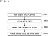
- FIG. 4 is a flowchart showing a sequence in manufacturing the bonded substrate in the first embodiment.
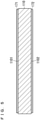
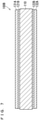
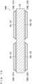
- FIGs. 5 , 6 , and 7 are cross-sectional views schematically showing intermediate products obtained in the process of manufacturing the bonded substrate in the first embodiment.
- steps S101 to S104 shown in FIG. 4 are sequentially performed.
- step S101 brazing material layers 171 and 172 are formed respectively on the main surfaces 1101 and 1102 of the silicon nitride ceramic substrate 110 as illustrated in FIG. 5 .
- the bonding layer 121 and the copper plate 131 are omitted from the bonded substrate 100
- formation of the brazing material layer 171 is omitted.
- the bonding layer 122 and the copper plate 132 are omitted from the bonded substrate 100
- formation of the brazing material layer 172 is omitted.
- a paste containing an active metal brazing material and a solvent is prepared.
- the paste may further contain a binder, a dispersant, an antifoaming agent, and the like.
- the prepared paste is then screen printed on the main surfaces 1101 and 1102 of the silicon nitride ceramic substrate 110 to form first and second screen printed films respectively on the main surfaces 1101 and 1102 of the silicon nitride ceramic substrate 110.
- the solvent contained in the formed first and second screen printed films is then volatilized.
- the first and second screen printed films are thereby respectively changed into the brazing material layers 171 and 172.
- the brazing material layers 171 and 172 each contain the active metal brazing material.
- the brazing material layers 171 and 172 may be formed by a method different from this method.
- the active metal brazing material includes metal powder containing silver (Ag), copper (Cu), and indium (In), and at least one metal hydride powder selected from the group consisting of titanium hydride powder and zirconium hydride powder.
- the composition of the active metal brazing material may be changed. For example, one or both of copper and indium may not be contained in the metal powder, and a metallic element other than copper and indium, such as tin (Sn), may be contained in the metal powder.
- the active metal brazing material preferably contains silver of 40 wt% or more and 80 wt% or less.
- the active metal brazing material contains such a small amount of silver, so that it is easy to diffuse silver into copper plates 131A and 132A to cause silver to disappear from bonding layers 121B and 122B in step S103, which will be described below.
- the active metal brazing material is preferably formed of powder having an average particle diameter of 0.1 ⁇ m or more and 10 ⁇ m or less.
- the average particle diameter can be obtained by measuring particle size distribution using a commercially available laser diffraction particle size distribution analyzer, and calculating D50 (a median diameter) from the measured particle size distribution.
- the active metal brazing material is formed of powder having such a small average particle diameter, so that the brazing material layers 171 and 172 can each have a small thickness.
- the brazing material layers 171 and 172 each preferably have a thickness of 0.1 ⁇ m or more and 10 ⁇ m or less, and more preferably have a thickness of 0.1 ⁇ m or more and 5 ⁇ m or less.
- the brazing material layers 171 and 172 each have such a small thickness, so that the brazing material layers 171 and 172 each contain a small amount of silver, and it is easy to diffuse silver into the copper plates 131A and 132A to cause silver to disappear from the bonding layers 121B and 122B in step S103, which will be described below.
- step S102 the copper plates 131A and 132A are disposed respectively on the formed brazing material layers 171 and 172 as illustrated in FIG. 6 .
- An intermediate product 100A including the silicon nitride ceramic substrate 110, the brazing material layer 171, the copper plate 131A, the brazing material layer 172, and the copper plate 132A is thereby obtained.
- the bonding layer 121 and the copper plate 131 are omitted from the bonded substrate 100
- disposition of the copper plate 131A is omitted.
- the bonding layer 122 and the copper plate 132 are omitted from the bonded substrate 100, disposition of the copper plate 132A is omitted.
- step S103 the obtained intermediate product 100A is thermally treated.
- the brazing material layers 171 and 172 are thereby respectively changed into the bonding layers 121B and 122B as illustrated in FIG. 7 , and an intermediate product 100B including the silicon nitride ceramic substrate 110, the bonding layer 121B, the copper plate 131A, the bonding layer 122B, and the copper plate 132A is obtained.
- the bonding layers 121B and 122B respectively bond the copper plates 131A and 132A to the silicon nitride ceramic substrate 110.
- the bonding layers 121B and 122B thus each contain a compound of at least one element selected from the group consisting of titanium and zirconium and at least one element selected from the group consisting of nitrogen and silicon, but do not contain silver and indium.
- the at least one element selected from the group consisting of nitrogen and silicon is supplied from the silicon nitride ceramic substrate 110.
- the first thickness-direction region 151 containing silver and having the first silver concentration and the second thickness-direction region 152 having the second silver concentration lower than the first silver concentration are formed.
- the intermediate product 100A is thermally treated, the intermediate product 100A is preferably hot pressed.
- the intermediate product 100A is preferably pressurized in a direction of the thickness of the silicon nitride ceramic substrate 110 in accordance with a contact pressure profile having a maximum contact pressure of 5 MPa or more and 25 MPa or less, and is heated in accordance with a temperature profile having a maximum temperature of 800 °C or more and 900 °C or less in a vacuum or an inert gas.
- the copper plates 131A and 132A can thereby be bonded to the silicon nitride ceramic substrate 110 without forming any void even when the brazing material layers 171 and 172 each have a small thickness as in the case where the brazing material layers 171 and 172 each have a thickness of 0.1 ⁇ m or more and 10 ⁇ m or less, for example.
- the brazing material layers 171 and 172 can each have a small thickness without forming any void, so that the brazing material layers 171 and 172 can each contain a small amount of silver, and it is easy to diffuse silver into the copper plates 131A and 132A to cause silver to disappear from the bonding layers 121B and 122B.
- the shape of particles constituting the active metal brazing material is changed into a layered shape, and silver and the like are diffused into the copper plates 131A and 132A, so that the bonding layers 121B and 122B each substantially have a thickness of 0.1 ⁇ m or more and 5 ⁇ m or less.
- step S104 the bonding layer 121B, the copper plate 131A, the bonding layer 122B, and the copper plate 132A are patterned.
- the bonding layers 121B and 122B are thereby respectively changed into the patterned bonding layers 121 and 122 illustrated in FIG. 1 .
- the copper plates 131A and 132A are respectively changed into the patterned copper plates 131 and 132 illustrated in FIG. 1 .
- FIG. 8 is a flowchart showing a sequence in patterning the bonding layers and the copper plates in the manufacture of the bonded substrate in the first embodiment.
- FIGs. 9 and 10 are cross-sectional views schematically showing intermediate products obtained in the process of patterning the bonding layers and the copper plates in the manufacture of the bonded substrate in the first embodiment.
- steps S111 to S113 shown in FIG. 8 are sequentially performed.
- step S111 the copper plates 131A and 132A are hard etched. Portions of the copper plates 131A and 132A are thereby removed, so that the copper plates 131A and 132A are respectively changed into etched copper plates 131C and 132C as illustrated in FIG. 9 .
- the bonding layer 121B a first portion 181 interposed between the silicon nitride ceramic substrate 110 and the etched copper plate 131C and a second portion 191 not interposed between the silicon nitride ceramic substrate 110 and the etched copper plate 131C are formed.
- a first portion 182 interposed between the silicon nitride ceramic substrate 110 and the etched copper plate 132C and a second portion 192 not interposed between the silicon nitride ceramic substrate 110 and the etched copper plate 132C are formed.
- An etchant such as an iron chloride aqueous solution and a copper chloride aqueous solution can be used for hard etching of the copper plates 131A and 132A.
- step S112 the formed second portions 191 and 192 are etched as illustrated in FIG. 10 .
- the second portions 191 and 192 are thus removed, and the first portions 181 and 182 remain.
- the remaining first portions 181 and 182 respectively serve as the bonding layers 121 and 122.
- An intermediate product 100C including the silicon nitride ceramic substrate 110, the bonding layer 121, the copper plate 131C, the bonding layer 122, and the copper plate 132C is thereby obtained.
- An etchant such as an ammonium fluoride aqueous solution can be used for etching of the second portions 191 and 192.
- opposite ends of each of the first portions 181 and 182 are sometimes etched.
- step S113 the etched copper plates 131C and 132C are soft etched. The vicinity of the ends of the etched copper plates 131C and 132C are thereby removed. The etched copper plates 131C and 132C are respectively changed into the patterned copper plates 131 and 132 illustrated in FIG. 1 .
- the interplate portion 160 and the protruding portion 161 illustrated in FIG. 1 are formed in each of the bonding layers 121 and 122.
- the etchant such as the iron chloride aqueous solution and the copper chloride aqueous solution can be used for soft etching of the copper plates 131C and 132C.
- the protruding portion 161 can surely be formed, even when the opposite ends of each of the first portions 181 and 182 are removed by etching in step S112.
- the first thickness-direction region 151 having the first silver concentration is etched at the first etching rate.
- the second thickness-direction region 152 having the second silver concentration lower than the first silver concentration is etched at the second etching rate faster than the first etching rate.
- the flared portion 1400 of the end surface 1303 is thereby formed.
- the flared portion 1400 is formed and the shape of the formed flared portion 1400 are dependent mainly on the amount of silver diffused into the copper plates 131A and 132A and severity of soft etching. Manufacturing conditions having the influence on the amount of silver diffused into the copper plates 131A and 132A and severity of soft etching are thus determined so that the flared portion 1400 having an appropriate shape is formed when the bonded substrate 100 is manufactured.
- determination is made considering that, with increasing amount of silver diffused into the copper plates 131A and 132A, the concentration of silver contained in the copper plates 131A and 132A increases, the distance by which silver is diffused into the copper plates 131A and 132A increases, the flared portion 1400 is more likely to be formed, and the formed flared portion 1400 is more likely to have the shape illustrated in FIG. 3 . Determination is made also considering that, with increasing severity of soft etching, the flared portion 1400 is more likely to be formed, and the formed flared portion 1400 is more likely to have the shape illustrated in FIG. 3 .
- An increase in amount of silver diffused into the copper plates 131A and 132A can be achieved by an increase in thickness of the brazing material layers 171 and 172, an increase in concentration of silver contained in the active metal brazing material, an increase in temperature when the intermediate product 100A is thermally treated, and the like.
- An increase in severity of soft etching can be achieved by an increase in temperature of the etchant used in soft etching, an increase in concentration of iron chloride, copper chloride, and the like contained in the etchant used in soft etching, an increase in time of contact of the copper plates 131C and 132C with the etchant used in soft etching, and the like.
- bonded substrates 100 were manufactured in accordance with the above-mentioned method of manufacturing the bonded substrate 100.
- the copper plates 131 and 132 each having a thickness of 0.8 mm were bonded to the silicon nitride ceramic substrate 110 having a thickness of 0.32 mm.
- the brazing material layers 171 and 172 each having a thickness of 0.1 ⁇ m or more and 5 ⁇ m or less and containing an active metal brazing material containing silver of 40 wt% or more and 80 wt% or less and a titanium hydride were formed.
- the intermediate product 100A was hot pressed.
- the intermediate product 100A was pressurized in accordance with a contact pressure profile having a maximum contact pressure of 20 MPa, and was heated in accordance with a temperature profile having a maximum temperature of 815 °C or more and 845 °C or less in a vacuum.
- Hard etching was performed by spraying an etchant at a temperature of approximately 45 °C onto the intermediate product 100B.
- Soft etching was performed by immersing the intermediate product 100C in an iron chloride aqueous solution as the etchant at a temperature of approximately 20 °C for 1.5 min. or more and 5 min. or less.
- the distance L1 was set to 100 ⁇ m or less.
- Comparative Example 1 a bonded substrate 100 was manufactured similarly to those in Examples 1 to 23 except that soft etching was not performed.
- bonded substrates 100 were manufactured similarly to those in Examples 1 to 23 except that the brazing material layers 171 and 172 each having a thickness of 0.1 ⁇ m or more and 1 ⁇ m or less and containing an active metal brazing material containing silver of 40 wt% or less and a titanium hydride were formed, the intermediate product 100A was heated in accordance with a temperature profile having a maximum temperature of 800 °C or less, and soft etching was performed by immersing the intermediate product 100C in an iron chloride aqueous solution as the etchant for 0.5 min. or more and 1 min. or less.
- a bonded substrate 100 was manufactured similarly to those in Examples 1 to 23 except that the brazing material layers 171 and 172 each having a thickness of 5 ⁇ m or less and containing an active metal brazing material containing silver of 60 wt% or more and 80 wt% or less and a titanium hydride were formed, the intermediate product 100A was heated in accordance with a temperature profile having a maximum temperature of 900 °C or more, and soft etching was performed by immersing the intermediate product 100C in an iron chloride aqueous solution as the etchant for 1.5 min.
- bonded substrates 100 were manufactured similarly to those in Examples 1 to 23 except that a copper plate having a flared portion having a predetermined shape obtained by cutting an end surface of a copper plate was used as each of the copper plates 132A and 132A disposed on the brazing material layers 171 and 172, and hard etching and soft etching were not performed.
- a bonded substrate 100 was manufactured similarly to those in Examples 1 to 23 except that soft etching was performed by immersing the intermediate product 100C in the etchant for 0.5 min. or less.
- Each of the manufactured bonded substrates 100 was processed to expose a cross section of the bonded substrate 100, and the exposed cross section was observed under a scanning electron microscope (SEM) to obtain an SEM image.
- SEM scanning electron microscope
- the angles ⁇ 1, ⁇ 2, and ⁇ 3 and the distance L2 were identified from the obtained SEM image. The results are shown in Tables 1 and 2.
- first thermal cycling durability of each of the manufactured bonded substrates 100 was evaluated.
- the bonded substrate 100 was subjected to thermal cycling of 3000 cycles.
- thermal cycling of each of 3000 cycles the bonded substrate 100 was sequentially subjected to a low temperature of -40 °C and a high temperature of 150 °C. The results are shown in Tables 1 and 2.
- second thermal cycling durability of each of the manufactured bonded substrates 100 was evaluated.
- the bonded substrate 100 was subjected to thermal cycling of 3000 cycles.
- thermal cycling of each of 3000 cycles the bonded substrate 100 was sequentially subjected to a low temperature of -55 °C and a high temperature of 175 °C. The results are shown in Tables 1 and 2.
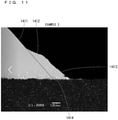
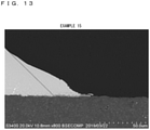
- FIGs. 11 , 12 , 13 , 14 , and 15 respectively show SEM images of cross sections of bonded substrates 100 manufactured in Examples 3, 4, 15, and 16 and Comparative Example 2.
- Distances L1 were 40 ⁇ m ( FIG. 11 ), 30 ⁇ m ( FIG. 12 ), 50 ⁇ m ( FIG. 13 ), 41 ⁇ m ( FIG. 14 ), and 49 ⁇ m ( FIG. 15 ) in Examples 3, 4, 15, and 16 and Comparative Example 2, respectively.
- the first thermal cycling durability is “OK”
- the second thermal cycling durability is “NG” in Examples 1 to 2 and 18 to 21 in each of which the flared portion 1400 has the shape illustrated in FIG. 2
- the angle ⁇ 1 is 135° or more and 165° or less
- the angle ⁇ 3 is 110° or more and 145° or less
- the distance L2 is 10 ⁇ m or more.
- the first thermal cycling durability and the second thermal cycling durability are each "OK" in Examples 3 to 16 and 22 to 23 in each of which the flared portion 1400 has the shape illustrated in FIG. 3 , the angles ⁇ 1 and ⁇ 2 are each 135° or more and 165° or less, the angle ⁇ 3 is 110° or more and 145° or less, and the distance L2 is 10 ⁇ m or more.
- the first thermal cycling durability and the second thermal cycling durability are each "NG" in Comparative Example 6 in which the flared portion 1400 has the shape illustrated in FIG. 2 , the angle ⁇ 1 is 135° or more and 165° or less, and the distance L2 is 10 ⁇ m or more, but the angle ⁇ 3 is less than 110°.
- the first thermal cycling durability and the second thermal cycling durability are each "NG" in Comparative Example 7 in which the flared portion 1400 has the shape illustrated in FIG. 2 , and the distance L2 is 10 ⁇ m or more, but the angle ⁇ 1 is less than 135°, and the angle ⁇ 3 is less than 110°.
- the first thermal cycling durability and the second thermal cycling durability are each "NG" in Comparative Example 8 in which the flared portion 1400 has the shape illustrated in FIG. 2 , and the distance L2 is 10 ⁇ m or more, but the angle ⁇ 1 is more than 165°, and the angle ⁇ 3 is more than 145°.
Landscapes
- Engineering & Computer Science (AREA)
- Chemical & Material Sciences (AREA)
- Ceramic Engineering (AREA)
- Microelectronics & Electronic Packaging (AREA)
- Manufacturing & Machinery (AREA)
- Materials Engineering (AREA)
- Structural Engineering (AREA)
- Organic Chemistry (AREA)
- Inorganic Chemistry (AREA)
- Ceramic Products (AREA)
- Structure Of Printed Boards (AREA)
- Manufacturing Of Printed Wiring (AREA)
Abstract
Description
- The present invention relates to bonded substrates and manufacturing methods of bonded substrates.
- Silicon nitride ceramics are highly heat conductive and highly insulating. A bonded substrate in which a copper plate is bonded to a silicon nitride ceramic substrate through a bonding layer is thus suitable for use as an insulating heat-dissipating substrate on which a power semiconductor device is mounted.
- In many cases, the bonded substrate is manufactured by preparing an intermediate product in which a brazing material layer is interposed between the copper plate and the silicon nitride ceramic substrate, changing the brazing material layer into the bonding layer through thermal treating on the prepared intermediate product, and patterning the copper plate and the bonding layer.
- Forming, in the bonding layer, a protruding portion protruding from between the silicon nitride ceramic substrate and the copper plate is proposed to suppress a defect of the bonded substrate caused by stress concentration on the end of the copper plate.
- In a ceramic circuit board disclosed in Patent Document 1, for example, a copper circuit plate is bonded, through a brazing material layer, to at least one surface of a ceramic substrate formed of silicon nitride (paragraphs 0013 and 0020). The ceramic circuit board includes a brazing material protruding portion protruding outward from a side surface of the copper circuit plate (paragraph 0013). This relieves thermal stress, so that a highly reliable ceramic-metal bonded circuit board can be achieved (paragraph 0013).
- Patent Document 1:
Japanese Patent No. 6271629 - In a conventional bonded substrate typified by the ceramic circuit board disclosed in Patent Document 1, a protruding portion protruding from between a silicon nitride ceramic substrate and a copper plate is formed to improve thermal cycling durability of the bonded substrate.
- However, improvement in thermal cycling durability of the bonded substrate is expected even when the protruding portion cannot be formed. As for the case that the protruding portion can be formed, further improvement in thermal cycling durability of the bonded substrate is expected.
- The present invention has been conceived in view of the problem. It is an object of the present invention to improve thermal cycling durability of a bonded substrate in which a copper plate is bonded to a silicon nitride ceramic substrate through a bonding layer.
- The present invention is directed to a bonded substrate.
- The bonded substrate includes a silicon nitride ceramic substrate, a bonding layer, and a copper plate.
- The bonding layer and the copper plate are disposed over the silicon nitride ceramic substrate.
- A second main surface of the copper plate is opposite a first main surface of the copper plate, and is bonded to the silicon nitride ceramic substrate by the bonding layer. An end surface of the copper plate extends from the first main surface of the copper plate to the second main surface of the copper plate.
- The end surface of the copper plate includes a first portion and a second portion. The second portion is closer to the second main surface than the first portion is.
- The first portion and the second portion form an angle of 135° or more and 165° or less on an outside of the copper plate. An extended plane of the first portion and the second main surface form an angle of 110° or more and 145° or less on a side where the second portion is located. A distance from the second main surface to an intersection of the first portion and the second portion in a direction of a thickness of the copper plate is 10 µm or more and 100 µm or less. The second main surface extends beyond the extended plane of the first portion by a distance of 10 µm or more.
- The present invention is also directed to a manufacturing method of a bonded substrate.
- In the manufacturing method of the bonded substrate, a brazing material layer is formed on a silicon nitride ceramic substrate. The brazing material layer contains an active metal brazing material. The active metal brazing material includes metal powder containing silver and at least one metal hydride powder selected from the group consisting of titanium hydride powder and zirconium hydride powder. The brazing material layer has a thickness of 0.1 µm or more and 10 µm or less.
- A copper plate is disposed on the brazing material layer. An intermediate product including the silicon nitride ceramic substrate, the brazing material layer, and the copper plate is thereby obtained.
- The intermediate product is thermally treated. The brazing material layer is thereby changed into a bonding layer to bond the copper plate to the silicon nitride ceramic substrate. Silver contained in the brazing material layer is diffused into the copper plate. A first thickness-direction region containing silver and having a first silver concentration and a second thickness-direction region having a second silver concentration lower than the first silver concentration are formed in the copper plate.
- The first thickness-direction region is etched at a first etching rate, and the second thickness-direction region is etched at a second etching rate faster than the first etching rate.
- When the bonded substrate is exposed to thermal cycling, stress is caused to be distributed to the vicinity of a corner between the first portion and the second portion and the vicinity of a corner between the second main surface and the end surface. Stress caused in the vicinity of each of the corners is thus reduced. Thermal cycling durability of the bonded substrate is thereby improved.
- The objects, features, aspects, and advantages of the present invention will become more apparent from the following detailed description and the accompanying drawings.
-
-
FIG. 1 is a cross-sectional view schematically showing a bonded substrate in a first embodiment. -
FIG. 2 is an enlarged cross-sectional view schematically showing a portion of the bonded substrate in the first embodiment. -
FIG. 3 is an enlarged cross-sectional view schematically showing a portion of the bonded substrate in the first embodiment. -
FIG. 4 is a flowchart showing a sequence in manufacturing the bonded substrate in the first embodiment. -
FIG. 5 is a cross-sectional view schematically showing an intermediate product obtained in the process of manufacturing the bonded substrate in the first embodiment. -
FIG. 6 is a cross-sectional view schematically showing an intermediate product obtained in the process of manufacturing the bonded substrate in the first embodiment. -
FIG. 7 is a cross-sectional view schematically showing an intermediate product obtained in the process of manufacturing the bonded substrate in the first embodiment. -
FIG. 8 is a flowchart showing a sequence in patterning bonding layers and copper plates in the manufacture of the bonded substrate in the first embodiment. -
FIG. 9 is a cross-sectional view schematically showing an intermediate product obtained in the process of patterning the bonding layers and the copper plates in the manufacture of the bonded substrate in the first embodiment. -
FIG. 10 is a cross-sectional view schematically showing an intermediate product obtained in the process of patterning the bonding layers and the copper plates in the manufacture of the bonded substrate in the first embodiment. -
FIG. 11 shows a scanning electron microscope (an SEM) image of a cross section of a bonded substrate manufactured in Example 3. -
FIG. 12 shows an SEM image of a cross section of a bonded substrate manufactured in Example 4. -
FIG. 13 shows an SEM image of a cross section of a bonded substrate manufactured in Example 15. -
FIG. 14 shows an SEM image of a cross section of a bonded substrate manufactured in Example 16. -
FIG. 15 shows an SEM image of a cross section of a bonded substrate manufactured in Comparative Example 2. -
FIG. 1 is a cross-sectional view schematically showing a bonded substrate in a first embodiment.FIGs. 2 and3 are enlarged cross-sectional views each schematically showing a portion of the bonded substrate in the first embodiment.FIGs. 2 and3 are each an enlarged view of a portion A ofFIG. 1 . - As illustrated in
FIG. 1 , a bondedsubstrate 100 in the first embodiment includes a siliconnitride ceramic substrate 110, a bonding layer 121, a copper plate 131, a bonding layer 122, and a copper plate 132. The bondedsubstrate 100 may include components other than these components. One of a pair of the bonding layer 121 and the copper plate 131 and a pair of the bonding layer 122 and the copper plate 132 may be omitted. - The bonding layer 121 and the copper plate 131 are disposed over a
main surface 1101 of the siliconnitride ceramic substrate 110. The bonding layer 122 and the copper plate 132 are disposed over amain surface 1102 of the siliconnitride ceramic substrate 110. - The copper plates 131 and 132 are bonded to the silicon
nitride ceramic substrate 110 respectively by the bonding layers 121 and 122. The copper plates 131 and 132 and themain surfaces nitride ceramic substrate 110 are brazed respectively by the bonding layers 121 and 122 by active metal brazing. - The bonded
substrate 100 may be intended for any applications, and is used, for example, as an insulating heat-dissipating substrate on which a power semiconductor device is mounted. - Hereinafter, each copper plate included in the copper plates 131 and 132 is referred to as a copper plate 130, and a bonding layer included in the bonding layers 121 and 122 to bond the copper plate 130 to the silicon
nitride ceramic substrate 110 is referred to as a bonding layer 120. - As illustrated in
FIG. 1 , the copper plate 130 has a firstmain surface 1301, a secondmain surface 1302, and anend surface 1303. The secondmain surface 1302 is opposite the firstmain surface 1301, and is bonded to the siliconnitride ceramic substrate 110 by the bonding layer 120. Theend surface 1303 extends from the firstmain surface 1301 to the secondmain surface 1302. - The
end surface 1303 has a flaredportion 1400 illustrated inFIG. 2 or3 . - When the
end surface 1303 has the flaredportion 1400 illustrated inFIG. 2 , theend surface 1303 includes afirst portion 1411 and asecond portion 1412. Thesecond portion 1412 is closer to the secondmain surface 1302 than thefirst portion 1411 is. Thefirst portion 1411 and thesecond portion 1412 are each substantially flat. - The
first portion 1411 and thesecond portion 1412 form an angle θ1 of 135° or more and 165° or less on the outside of the copper plate 130. Anextended plane 1414 of thefirst portion 1411 and the secondmain surface 1302 form an angle θ3 of 110° or more and 145° or less on a side where thesecond portion 1412 is located. Anintersection 1421 of thefirst portion 1411 and thesecond portion 1412 is preferably separated from the secondmain surface 1302 by a distance L1 of 10 µm or more and 100 µm or less in a direction of the thickness of the copper plate 130, and is more preferably separated from the secondmain surface 1302 by a distance L1 of 10 µm or more and 60 µm or less in the direction of the thickness of the copper plate 130. The secondmain surface 1302 extends beyond theextended plane 1414 of thefirst portion 1411 by a distance L2 of 10 µm or more. A direction of a normal to theextended plane 1414 is the same as a direction of a normal to thefirst portion 1411 at a location closest to the secondmain surface 1302. - The copper plate 130 has a
corner 1421 between thefirst portion 1411 and thesecond portion 1412 and acorner 1423 between the secondmain surface 1302 and theend surface 1303. When the bondedsubstrate 100 is exposed to thermal cycling, stress is caused to be distributed to the vicinity of thecorner 1421 and the vicinity of thecorner 1423. Stress caused in the vicinity of each of thecorners substrate 100 is thereby improved. - When the angle θ1 is less than 135°, stress is excessively concentrated on the vicinity of the
corner 1421, and obtaining an effect of improving thermal cycling durability of the bondedsubstrate 100 tends to be difficult. When the angle θ1 is more than 165°, stress is not distributed to the vicinity of thecorner 1421, and obtaining the effect of improving thermal cycling durability of the bondedsubstrate 100 tends to be difficult. When the angle θ3 is less than 110°, stress is concentrated on the flaredportion 1400, and obtaining the effect of improving thermal cycling durability of the bondedsubstrate 100 tends to be difficult. When the angle θ3 is more than 145°, stress is not distributed to the flaredportion 1400, and obtaining the effect of improving thermal cycling durability of the bondedsubstrate 100 tends to be difficult. Thermal cycling durability of the bondedsubstrate 100 can further be improved when the distance L1 is 10 µm or more and 100 µm or less, and thermal cycling durability of the bondedsubstrate 100 can particularly be improved when the distance L1 is 10 µm or more and 60 µm or less. When the distance L1 is less than these ranges, thecorners substrate 100 tends to be difficult. When the distance L1 is more than these ranges, stress is not caused in the vicinity of thecorner 1421, and obtaining the effect of improving thermal cycling durability of the bondedsubstrate 100 tends to be difficult. When the distance L2 is less than 10 µm, stress is not distributed, and obtaining the effect of improving thermal cycling durability of the bondedsubstrate 100 tends to be difficult. - When the
end surface 1303 has the flaredportion 1400 illustrated inFIG. 3 , theend surface 1303 includes thefirst portion 1411, thesecond portion 1412, and athird portion 1413. Thesecond portion 1412 is closer to the secondmain surface 1302 than thefirst portion 1411 is. Thethird portion 1413 is closer to the secondmain surface 1302 than thesecond portion 1412 is. Thefirst portion 1411, thesecond portion 1412, and thethird portion 1413 are each substantially flat. - The
first portion 1411 and thesecond portion 1412 form the angle θ1 of 135° or more and 165° or less on the outside of the copper plate 130. Thesecond portion 1412 and thethird portion 1413 form an angle θ2 of 135° or more and 165° or less on the inside of the copper plate 130. Theextended plane 1414 of thefirst portion 1411 and the secondmain surface 1302 form the angle θ3 of 110° or more and 145° or less on the side where thesecond portion 1412 is located. Theintersection 1421 of thefirst portion 1411 and thesecond portion 1412 is preferably separated from the secondmain surface 1302 by the distance L1 of 10 µm or more and 100 µm or less in the direction of the thickness of the copper plate 130, and is more preferably separated from the secondmain surface 1302 by the distance L1 of 10 µm or more and 60 µm or less in the direction of the thickness of the copper plate 130. The secondmain surface 1302 extends beyond theextended plane 1414 of thefirst portion 1411 by the distance L2 of 10 µm or more. The direction of the normal to theextended plane 1414 is the same as the direction of the normal to thefirst portion 1411 at the location closest to the secondmain surface 1302. - The copper plate 130 has the
corner 1421 between thefirst portion 1411 and thesecond portion 1412, acorner 1422 between thesecond portion 1412 and thethird portion 1413, and thecorner 1423 between the secondmain surface 1302 and theend surface 1303. When the bondedsubstrate 100 is exposed to thermal cycling, stress is caused to be distributed to the vicinity of thecorner 1421, the vicinity of thecorner 1422, and the vicinity of thecorner 1423. Stress caused in the vicinity of each of thecorners substrate 100 is thereby improved. Stress is distributed not only to the vicinity of thecorner 1421 and the vicinity of thecorner 1422 but also to the vicinity of thecorner 1423, so that thermal cycling durability of the bondedsubstrate 100 is further improved compared with a case where stress is distributed only to the vicinity of thecorner 1421 and the vicinity of thecorner 1423. - When the angle θ1 is less than 135°, stress is excessively concentrated on the vicinity of the
corner 1421, and obtaining the effect of improving thermal cycling durability of the bondedsubstrate 100 tends to be difficult. When the angle θ1 is more than 165°, stress is not distributed to the vicinity of thecorner 1421, and obtaining the effect of improving thermal cycling durability of the bondedsubstrate 100 tends to be difficult. The same applies to the angle θ2. When the angle θ3 is less than 110°, stress is concentrated on the flaredportion 1400, and obtaining the effect of improving thermal cycling durability of the bondedsubstrate 100 tends to be difficult. When the angle θ3 is more than 145°, stress is not distributed to the flaredportion 1400, and obtaining the effect of improving thermal cycling durability of the bondedsubstrate 100 tends to be difficult. Thermal cycling durability of the bondedsubstrate 100 can further be improved when the distance L1 is 10 µm or more and 100 µm or less, and thermal cycling durability of the bondedsubstrate 100 can particularly be improved when the distance L1 is 10 µm or more and 60 µm or less. When the distance L1 is less than these ranges, thecorners substrate 100 tends to be difficult. When the distance L1 is more than these ranges, stress is not distributed to the vicinity of thecorner 1421 and the vicinity of thecorner 1422, and obtaining the effect of improving thermal cycling durability of the bondedsubstrate 100 tends to be difficult. When the distance L2 is less than 10 µm, stress is not distributed, and obtaining the effect of improving thermal cycling durability of the bondedsubstrate 100 tends to be difficult. - The copper plate 130 has silver concentration distribution in which a silver concentration decreases with increasing distance from the second
main surface 1302. The silver concentration decreases with increasing distance from the secondmain surface 1302 because silver is diffused from a brazing material layer as a precursor of the bonding layer 120 into the copper plate 130 in the process of manufacturing the bondedsubstrate 100. - The copper plate 130 thus includes a first thickness-
direction region 151 containing silver and having a first silver concentration and a second thickness-direction region 152 having a second silver concentration lower than the first silver concentration as illustrated inFIGs. 2 and3 . A state of the second thickness-direction region 152 having the second silver concentration lower than the first silver concentration includes both of a state of the second thickness-direction region 152 not containing silver and a state of the second thickness-direction region 152 containing silver but having the second silver concentration lower than the first silver concentration, and the former is preferable. - When the
end surface 1303 has the flaredportion 1400 illustrated inFIG. 2 , the first thickness-direction region 151 has thesecond portion 1412. When theend surface 1303 has the flaredportion 1400 illustrated inFIG. 3 , the first thickness-direction region 151 has thesecond portion 1412 and thethird portion 1413. The second thickness-direction region 152 has thefirst portion 1411. - The first thickness-
direction region 151 has a first etching rate for an etchant for the copper plate 130. The second thickness-direction region 152 has a second etching rate for the etchant. The second etching rate is faster than the first etching rate. The second etching rate is faster than the first etching rate because the second silver concentration is lower than the first silver concentration. - The flared
portion 1400 of theend surface 1303 is formed by etching utilizing the relationship that the second etching rate is faster than the first etching rate. The flaredportion 1400 of theend surface 1303 may be formed by a method other than etching. For example, the flaredportion 1400 of theend surface 1303 may be formed by machining. - The bonding layer 120 includes an
interplate portion 160 and a protrudingportion 161 as illustrated inFIGs. 1 ,2 , and3 . Theinterplate portion 160 is interposed between the siliconnitride ceramic substrate 110 and the copper plate 130. The protrudingportion 161 protrudes from between the siliconnitride ceramic substrate 110 and the copper plate 130. In the bondedsubstrate 100, stress concentration on the end of the copper plate 130 is relieved by the protrudingportion 161. A defect of the bondedsubstrate 100 caused by stress concentration on the end of the copper plate 130 can thereby be suppressed. - The bonding layer 120 preferably has a thickness of 0.1 µm or more and 5 µm or less, and more preferably has a thickness of 0.1 µm or more and 3 µm or less. The bonding layer 120 has such a small thickness, so that stress concentration on the end of the copper plate 130 is effectively relieved by the protruding
portion 161. - The copper plate 130 preferably has a thickness of 0.5 mm or more. When the copper plate 130 has a thickness of 0.5 mm or more, the bonded
substrate 100 being highly heat dissipating can be obtained. On the other hand, when the copper plate 130 has a thickness of 0.5 mm or more, large stress is caused in the copper plate 130, and thermal cycling durability of the bondedsubstrate 100 tends to be reduced. In the bondedsubstrate 100, however, the above-mentioned effect of improving thermal cycling durability of the bondedsubstrate 100 can compensate for reduction in thermal cycling durability of the bondedsubstrate 100 when the copper plate 130 has a thickness of 0.5 mm or more. - The distance L2 is preferably 100 µm or less, more preferably 60 µm or less, even more preferably 40 µm, and most preferably 30 µm or less. When the distance L2 is more than these upper limits, adjacent two copper plates 130 are brought closer to each other, and insulation between the adjacent two copper plates 130 tends to be reduced.
-
FIG. 4 is a flowchart showing a sequence in manufacturing the bonded substrate in the first embodiment.FIGs. 5 ,6 , and7 are cross-sectional views schematically showing intermediate products obtained in the process of manufacturing the bonded substrate in the first embodiment. - In the manufacture of the bonded
substrate 100 in the first embodiment, steps S101 to S104 shown inFIG. 4 are sequentially performed. - In step S101, brazing
material layers main surfaces nitride ceramic substrate 110 as illustrated inFIG. 5 . When the bonding layer 121 and the copper plate 131 are omitted from the bondedsubstrate 100, formation of thebrazing material layer 171 is omitted. When the bonding layer 122 and the copper plate 132 are omitted from the bondedsubstrate 100, formation of thebrazing material layer 172 is omitted. - When the brazing material layers 171 and 172 are formed, a paste containing an active metal brazing material and a solvent is prepared. The paste may further contain a binder, a dispersant, an antifoaming agent, and the like. The prepared paste is then screen printed on the
main surfaces nitride ceramic substrate 110 to form first and second screen printed films respectively on themain surfaces nitride ceramic substrate 110. The solvent contained in the formed first and second screen printed films is then volatilized. The first and second screen printed films are thereby respectively changed into the brazing material layers 171 and 172. The brazing material layers 171 and 172 each contain the active metal brazing material. The brazing material layers 171 and 172 may be formed by a method different from this method. - The active metal brazing material includes metal powder containing silver (Ag), copper (Cu), and indium (In), and at least one metal hydride powder selected from the group consisting of titanium hydride powder and zirconium hydride powder. The composition of the active metal brazing material may be changed. For example, one or both of copper and indium may not be contained in the metal powder, and a metallic element other than copper and indium, such as tin (Sn), may be contained in the metal powder.
- The active metal brazing material preferably contains silver of 40 wt% or more and 80 wt% or less. The active metal brazing material contains such a small amount of silver, so that it is easy to diffuse silver into
copper plates layers - The active metal brazing material is preferably formed of powder having an average particle diameter of 0.1 µm or more and 10 µm or less. The average particle diameter can be obtained by measuring particle size distribution using a commercially available laser diffraction particle size distribution analyzer, and calculating D50 (a median diameter) from the measured particle size distribution. The active metal brazing material is formed of powder having such a small average particle diameter, so that the brazing material layers 171 and 172 can each have a small thickness.
- The brazing material layers 171 and 172 each preferably have a thickness of 0.1 µm or more and 10 µm or less, and more preferably have a thickness of 0.1 µm or more and 5 µm or less. The brazing material layers 171 and 172 each have such a small thickness, so that the brazing material layers 171 and 172 each contain a small amount of silver, and it is easy to diffuse silver into the
copper plates - In step S102, the
copper plates FIG. 6 . Anintermediate product 100A including the siliconnitride ceramic substrate 110, thebrazing material layer 171, thecopper plate 131A, thebrazing material layer 172, and thecopper plate 132A is thereby obtained. When the bonding layer 121 and the copper plate 131 are omitted from the bondedsubstrate 100, disposition of thecopper plate 131A is omitted. When the bonding layer 122 and the copper plate 132 are omitted from the bondedsubstrate 100, disposition of thecopper plate 132A is omitted. - In step S103, the obtained
intermediate product 100A is thermally treated. - The brazing material layers 171 and 172 are thereby respectively changed into the bonding layers 121B and 122B as illustrated in
FIG. 7 , and anintermediate product 100B including the siliconnitride ceramic substrate 110, thebonding layer 121B, thecopper plate 131A, thebonding layer 122B, and thecopper plate 132A is obtained. The bonding layers 121B and 122B respectively bond thecopper plates nitride ceramic substrate 110. While the brazing material layers 171 and 172 are respectively changed into the bonding layers 121B and 122B, silver and indium contained in the brazing material layers 171 and 172 are respectively diffused into thecopper plates nitride ceramic substrate 110. In each of thecopper plates direction region 151 containing silver and having the first silver concentration and the second thickness-direction region 152 having the second silver concentration lower than the first silver concentration are formed. - When the
intermediate product 100A is thermally treated, theintermediate product 100A is preferably hot pressed. When theintermediate product 100A is hot pressed, theintermediate product 100A is preferably pressurized in a direction of the thickness of the siliconnitride ceramic substrate 110 in accordance with a contact pressure profile having a maximum contact pressure of 5 MPa or more and 25 MPa or less, and is heated in accordance with a temperature profile having a maximum temperature of 800 °C or more and 900 °C or less in a vacuum or an inert gas. Thecopper plates nitride ceramic substrate 110 without forming any void even when the brazing material layers 171 and 172 each have a small thickness as in the case where the brazing material layers 171 and 172 each have a thickness of 0.1 µm or more and 10 µm or less, for example. The brazing material layers 171 and 172 can each have a small thickness without forming any void, so that the brazing material layers 171 and 172 can each contain a small amount of silver, and it is easy to diffuse silver into thecopper plates copper plates - In step S104, the
bonding layer 121B, thecopper plate 131A, thebonding layer 122B, and thecopper plate 132A are patterned. The bonding layers 121B and 122B are thereby respectively changed into the patterned bonding layers 121 and 122 illustrated inFIG. 1 . Thecopper plates FIG. 1 . -
FIG. 8 is a flowchart showing a sequence in patterning the bonding layers and the copper plates in the manufacture of the bonded substrate in the first embodiment.FIGs. 9 and10 are cross-sectional views schematically showing intermediate products obtained in the process of patterning the bonding layers and the copper plates in the manufacture of the bonded substrate in the first embodiment. - In patterning the
bonding layer 121B, thecopper plate 131A, thebonding layer 122B, and thecopper plate 132A in the manufacture of the bondedsubstrate 100 in the first embodiment, steps S111 to S113 shown inFIG. 8 are sequentially performed. - In step S111, the
copper plates copper plates copper plates copper plates FIG. 9 . In thebonding layer 121B, afirst portion 181 interposed between the siliconnitride ceramic substrate 110 and the etchedcopper plate 131C and asecond portion 191 not interposed between the siliconnitride ceramic substrate 110 and the etchedcopper plate 131C are formed. In thebonding layer 122B, afirst portion 182 interposed between the siliconnitride ceramic substrate 110 and the etchedcopper plate 132C and asecond portion 192 not interposed between the siliconnitride ceramic substrate 110 and the etchedcopper plate 132C are formed. An etchant such as an iron chloride aqueous solution and a copper chloride aqueous solution can be used for hard etching of thecopper plates - In step S112, the formed
second portions FIG. 10 . Thesecond portions first portions first portions nitride ceramic substrate 110, the bonding layer 121, thecopper plate 131C, the bonding layer 122, and thecopper plate 132C is thereby obtained. An etchant such as an ammonium fluoride aqueous solution can be used for etching of thesecond portions first portions - In step S113, the etched
copper plates copper plates copper plates FIG. 1 . Theinterplate portion 160 and the protrudingportion 161 illustrated inFIG. 1 are formed in each of the bonding layers 121 and 122. The etchant such as the iron chloride aqueous solution and the copper chloride aqueous solution can be used for soft etching of thecopper plates portion 161 can surely be formed, even when the opposite ends of each of thefirst portions - When each
copper plate 130C included in thecopper plates direction region 151 having the first silver concentration is etched at the first etching rate. The second thickness-direction region 152 having the second silver concentration lower than the first silver concentration is etched at the second etching rate faster than the first etching rate. The flaredportion 1400 of theend surface 1303 is thereby formed. - Whether the flared
portion 1400 is formed and the shape of the formed flaredportion 1400 are dependent mainly on the amount of silver diffused into thecopper plates copper plates portion 1400 having an appropriate shape is formed when the bondedsubstrate 100 is manufactured. In this case, determination is made considering that, with increasing amount of silver diffused into thecopper plates copper plates copper plates portion 1400 is more likely to be formed, and the formed flaredportion 1400 is more likely to have the shape illustrated inFIG. 3 . Determination is made also considering that, with increasing severity of soft etching, the flaredportion 1400 is more likely to be formed, and the formed flaredportion 1400 is more likely to have the shape illustrated inFIG. 3 . - An increase in amount of silver diffused into the
copper plates intermediate product 100A is thermally treated, and the like. - An increase in severity of soft etching can be achieved by an increase in temperature of the etchant used in soft etching, an increase in concentration of iron chloride, copper chloride, and the like contained in the etchant used in soft etching, an increase in time of contact of the
copper plates - In Examples 1 to 23, bonded
substrates 100 were manufactured in accordance with the above-mentioned method of manufacturing the bondedsubstrate 100. - In each of Examples 1 to 23, the copper plates 131 and 132 each having a thickness of 0.8 mm were bonded to the silicon
nitride ceramic substrate 110 having a thickness of 0.32 mm. The brazing material layers 171 and 172 each having a thickness of 0.1 µm or more and 5 µm or less and containing an active metal brazing material containing silver of 40 wt% or more and 80 wt% or less and a titanium hydride were formed. Theintermediate product 100A was hot pressed. In this case, theintermediate product 100A was pressurized in accordance with a contact pressure profile having a maximum contact pressure of 20 MPa, and was heated in accordance with a temperature profile having a maximum temperature of 815 °C or more and 845 °C or less in a vacuum. Hard etching was performed by spraying an etchant at a temperature of approximately 45 °C onto theintermediate product 100B. Soft etching was performed by immersing the intermediate product 100C in an iron chloride aqueous solution as the etchant at a temperature of approximately 20 °C for 1.5 min. or more and 5 min. or less. The distance L1 was set to 100 µm or less. - In Comparative Example 1, a bonded
substrate 100 was manufactured similarly to those in Examples 1 to 23 except that soft etching was not performed. - In Comparative Examples 2 to 4, bonded
substrates 100 were manufactured similarly to those in Examples 1 to 23 except that the brazing material layers 171 and 172 each having a thickness of 0.1 µm or more and 1 µm or less and containing an active metal brazing material containing silver of 40 wt% or less and a titanium hydride were formed, theintermediate product 100A was heated in accordance with a temperature profile having a maximum temperature of 800 °C or less, and soft etching was performed by immersing the intermediate product 100C in an iron chloride aqueous solution as the etchant for 0.5 min. or more and 1 min. or less. - In Comparative Example 5, a bonded
substrate 100 was manufactured similarly to those in Examples 1 to 23 except that the brazing material layers 171 and 172 each having a thickness of 5 µm or less and containing an active metal brazing material containing silver of 60 wt% or more and 80 wt% or less and a titanium hydride were formed, theintermediate product 100A was heated in accordance with a temperature profile having a maximum temperature of 900 °C or more, and soft etching was performed by immersing the intermediate product 100C in an iron chloride aqueous solution as the etchant for 1.5 min. - In Comparative Examples 6 and 7, bonded
substrates 100 were manufactured similarly to those in Examples 1 to 23 except that a copper plate having a flared portion having a predetermined shape obtained by cutting an end surface of a copper plate was used as each of thecopper plates substrate 100 was manufactured similarly to those in Examples 1 to 23 except that soft etching was performed by immersing the intermediate product 100C in the etchant for 0.5 min. or less. - Each of the manufactured bonded
substrates 100 was processed to expose a cross section of the bondedsubstrate 100, and the exposed cross section was observed under a scanning electron microscope (SEM) to obtain an SEM image. The angles θ1, θ2, and θ3 and the distance L2 were identified from the obtained SEM image. The results are shown in Tables 1 and 2. - In addition, first thermal cycling durability of each of the manufactured bonded
substrates 100 was evaluated. In evaluating the first thermal cycling durability, the bondedsubstrate 100 was subjected to thermal cycling of 3000 cycles. In thermal cycling of each of 3000 cycles, the bondedsubstrate 100 was sequentially subjected to a low temperature of -40 °C and a high temperature of 150 °C. The results are shown in Tables 1 and 2. - In addition, second thermal cycling durability of each of the manufactured bonded
substrates 100 was evaluated. In evaluating the second thermal cycling durability, the bondedsubstrate 100 was subjected to thermal cycling of 3000 cycles. In thermal cycling of each of 3000 cycles, the bondedsubstrate 100 was sequentially subjected to a low temperature of -55 °C and a high temperature of 175 °C. The results are shown in Tables 1 and 2. - In each of Tables 1 and 2, "OK" indicates that it was confirmed in an ultrasonic test that, after the bonded
substrate 100 was subjected to thermal cycling of 3000 cycles, the copper plates 131 and 132 were not separated from the siliconnitride ceramic substrate 110, and cracking of the siliconnitride ceramic substrate 110 did not occur. In each of Tables 1 and 2, "NG" indicates the opposite. -
FIGs. 11 ,12 ,13 ,14 , and15 respectively show SEM images of cross sections of bondedsubstrates 100 manufactured in Examples 3, 4, 15, and 16 and Comparative Example 2. Distances L1 were 40 µm (FIG. 11 ), 30 µm (FIG. 12 ), 50 µm (FIG. 13 ), 41 µm (FIG. 14 ), and 49 µm (FIG. 15 ) in Examples 3, 4, 15, and 16 and Comparative Example 2, respectively.[Table 1] θ1(°) θ2(°) θ3(°) L2(µm) FIRST THERMAL CYCLING DURABILITY SECOND THERMAL CYCLING DURABILITY -40 °C/150 °C 3000 CYCLES OK/NG -55 °C/175 °C 3000 CYCLES OK/NG EXAMPLE 1 165 - 122 10.5 OK NG EXAMPLE 2 135 - 117 35 OK NG EXAMPLE 3 155 163 132 20.4 OK OK EXAMPLE 4 160 165 131 13.1 OK OK EXAMPLE 5 150 150 125 10.3 OK OK EXAMPLE 6 155 165 125 27.6 OK OK EXAMPLE 7 139 135 138 10.8 OK OK EXAMPLE 8 135 135 127 30.7 OK OK EXAMPLE 9 139 155 133 10.4 OK OK EXAMPLE 10 135 165 133 30.9 OK OK EXAMPLE 11 165 135 130 10.2 OK OK EXAMPLE 12 165 145 138 29.7 OK OK EXAMPLE 13 165 165 122 10.3 OK OK EXAMPLE 14 165 165 141 29.6 OK OK EXAMPLE 15 162 165 136 35 OK OK EXAMPLE 16 136 151 128 39 OK OK EXAMPLE 17 127 135 127 58 OK OK EXAMPLE 18 138 - 141 30 OK NG EXAMPLE 19 148 - 124 25 OK NG EXAMPLE 20 153 - 141 15 OK NG EXAMPLE 21 162 - 113 10.2 OK NG EXAMPLE 22 140 155 110 31.9 OK OK EXAMPLE 23 160 163 145 34.1 OK OK [Table 2] θ1(°) θ2(°) θ3(°) L2(µm) FIRST THERMAL CYCLING DURABILITY SECOND THERMAL CYCLING DURABILITY -40 °C/150 °C 3000 CYCLES OK/NG - 55 °C/175 °C 3000 CYCLES OK/NG COMPARATIVE EXAMPLE 1 - - 130 - NG NG COMPARATIVE EXAMPLE 2 165 165 137 9 NG NG COMPARATIVE EXAMPLE 3 170 175 131 5 NG NG COMPARATIVE EXAMPLE 4 170 170 130 15 NG NG COMPARATIVE EXAMPLE 5 133 131 125 9 NG NG COMPARATIVE EXAMPLE 6 135 - 90 30 NG NG COMPARATIVE EXAMPLE 7 108 - 90 70 NG NG COMPARATIVE EXAMPLE 8 176 - 150 10 NG NG - It can be understood from Table 1 that the first thermal cycling durability is "OK", but the second thermal cycling durability is "NG" in Examples 1 to 2 and 18 to 21 in each of which the flared
portion 1400 has the shape illustrated inFIG. 2 , the angle θ1 is 135° or more and 165° or less, the angle θ3 is 110° or more and 145° or less, and the distance L2 is 10 µm or more. - It can also be understood from Table 1 and SEM images that the first thermal cycling durability and the second thermal cycling durability are each "OK" in Examples 3 to 16 and 22 to 23 in each of which the flared
portion 1400 has the shape illustrated inFIG. 3 , the angles θ1 and θ2 are each 135° or more and 165° or less, the angle θ3 is 110° or more and 145° or less, and the distance L2 is 10 µm or more. - It can also be understood from Table 1 and an SEM image that the first thermal cycling durability and the second thermal cycling durability are each "NG" in Comparative Example 1 in which the flared
portion 1400 does not have the shape illustrated inFIG. 2 or3 . - It can also be understood from Table 1 and an SEM image that the first thermal cycling durability and the second thermal cycling durability are each "NG" in Comparative Example 2 in which the flared
portion 1400 has the shape illustrated inFIG. 3 , and the angles θ1 and θ2 are each 135° or more and 165° or less, but the distance L2 is less than 10 µm. - It can also be understood from Table 1 and an SEM image that the first thermal cycling durability and the second thermal cycling durability are each "NG" in Comparative Example 3 in which the flared
portion 1400 has the shape illustrated inFIG. 3 , but the angles θ1 and θ2 are each more than 165°, and the distance L2 is less than 10 µm. - It can also be understood from Table 1 and an SEM image that the first thermal cycling durability and the second thermal cycling durability are each "NG" in Comparative Example 4 in which the flared
portion 1400 has the shape illustrated inFIG. 3 , and the distance L2 is 10 µm or more, but the angles θ1 and θ2 are each more than 165°. - It can also be understood from Table 1 and an SEM image that the first thermal cycling durability and the second thermal cycling durability are each "NG" in Comparative Example 5 in which the flared
portion 1400 has the shape illustrated inFIG. 3 , but the angles θ1 and θ2 are each less than 135°, and the distance L2 is less than 10 µm. - It can also be understood from Table 1 that the first thermal cycling durability and the second thermal cycling durability are each "NG" in Comparative Example 6 in which the flared
portion 1400 has the shape illustrated inFIG. 2 , the angle θ1 is 135° or more and 165° or less, and the distance L2 is 10 µm or more, but the angle θ3 is less than 110°. - It can also be understood from Table 1 that the first thermal cycling durability and the second thermal cycling durability are each "NG" in Comparative Example 7 in which the flared
portion 1400 has the shape illustrated inFIG. 2 , and the distance L2 is 10 µm or more, but the angle θ1 is less than 135°, and the angle θ3 is less than 110°. - It can also be understood from Table 1 that the first thermal cycling durability and the second thermal cycling durability are each "NG" in Comparative Example 8 in which the flared
portion 1400 has the shape illustrated inFIG. 2 , and the distance L2 is 10 µm or more, but the angle θ1 is more than 165°, and the angle θ3 is more than 145°. - While the invention has been described in detail, the foregoing description is in all aspects illustrative and not restrictive. It is therefore understood that numerous unillustrated modifications can be devised without departing from the scope of the invention.
-
- 100
- bonded substrate
- 110
- silicon nitride ceramic substrate
- 121, 122
- bonding layer
- 131, 132
- copper plate
- 1301
- first main surface
- 1302
- second main surface
- 1303
- end surface
- 1411
- first portion
- 1412
- second portion
- 1413
- third portion
Claims (6)
- A bonded substrate comprising:a silicon nitride ceramic substrate;a bonding layer disposed over the silicon nitride ceramic substrate; anda copper plate disposed over the silicon nitride ceramic substrate, and having a first main surface, a second main surface, and an end surface, the second main surface being opposite the first main surface and bonded to the silicon nitride ceramic substrate by the bonding layer, the end surface extending from the first main surface to the second main surface, whereinthe end surface includes:a first portion; anda second portion closer to the second main surface than the first portion is,the first portion and the second portion form an angle of 135° or more and 165° or less on an outside of the copper plate,an extended plane of the first portion and the second main surface form an angle of 110° or more and 145° or less on a side where the second portion is located,a distance from the second main surface to an intersection of the first portion and the second portion in a direction of a thickness of the copper plate is 10 µm or more and 100 µm or less, andthe second main surface extends beyond the extended plane of the first portion by a distance of 10 µm or more.
- The bonded substrate according to claim 1, wherein
the end surface further includes a third portion closer to the second main surface than the second portion is, and
the second portion and the third portion form an angle of 135° or more and 165° or less on an inside of the copper plate. - The bonded substrate according to claim 1 or 2, wherein
the copper plate includes:a first thickness-direction region having the second portion, containing silver, and having a first silver concentration; anda second thickness-direction region having the first portion, and having a second silver concentration lower than the first silver concentration. - The bonded substrate according to any one of claims 1 to 3, wherein
the bonding layer includes:an interplate portion between the silicon nitride ceramic substrate and the copper plate; andan protruding portion protruding from between the silicon nitride ceramic substrate and the copper plate. - The bonded substrate according to any one of claims 1 to 4, wherein
the copper plate has a thickness of 0.5 mm or more. - A bonded substrate manufacturing method comprising:a) forming, on a silicon nitride ceramic substrate, a brazing material layer containing an active metal brazing material and having a thickness of 0.1 µm or more and 10 µm or less, the active metal brazing material including metal powder containing silver and at least one metal hydride powder selected from the group consisting of titanium hydride powder and zirconium hydride powder;b) disposing a copper plate on the brazing material layer to obtain an intermediate product including the silicon nitride ceramic substrate, the brazing material layer, and the copper plate;c) thermally treating the intermediate product to change the brazing material layer into a bonding layer to bond the copper plate to the silicon nitride ceramic substrate, and diffusing silver contained in the brazing material layer into the copper plate to form, in the copper plate, a first thickness-direction region containing silver and having a first silver concentration and a second thickness-direction region having a second silver concentration lower than the first silver concentration; andd) etching the first thickness-direction region at a first etching rate, and etching the second thickness-direction region at a second etching rate faster than the first etching rate.
Applications Claiming Priority (2)
| Application Number | Priority Date | Filing Date | Title |
|---|---|---|---|
| PCT/JP2019/015414 WO2020208698A1 (en) | 2019-04-09 | 2019-04-09 | Bonded substrate and method for manufacturing bonded substrate |
| PCT/JP2020/014514 WO2020209121A1 (en) | 2019-04-09 | 2020-03-30 | Bonded substrate and method for producing bonded substrate |
Publications (2)
| Publication Number | Publication Date |
|---|---|
| EP3955284A1 true EP3955284A1 (en) | 2022-02-16 |
| EP3955284A4 EP3955284A4 (en) | 2023-09-20 |
Family
ID=72751554
Family Applications (1)
| Application Number | Title | Priority Date | Filing Date |
|---|---|---|---|
| EP20787489.2A Pending EP3955284A4 (en) | 2019-04-09 | 2020-03-30 | BONDED SUBSTRATE AND METHOD FOR PRODUCING A BONDED SUBSTRATE |
Country Status (4)
| Country | Link |
|---|---|
| US (1) | US11917752B2 (en) |
| EP (1) | EP3955284A4 (en) |
| JP (2) | JP7289911B2 (en) |
| WO (2) | WO2020208698A1 (en) |
Cited By (1)
| Publication number | Priority date | Publication date | Assignee | Title |
|---|---|---|---|---|
| EP4593075A1 (en) * | 2024-01-24 | 2025-07-30 | Heraeus Electronics GmbH & Co. KG | Metal-ceramic substrate with contact area |
Families Citing this family (7)
| Publication number | Priority date | Publication date | Assignee | Title |
|---|---|---|---|---|
| JP7666202B2 (en) * | 2021-07-30 | 2025-04-22 | 三菱マテリアル株式会社 | Copper/ceramic bonded body and insulated circuit board |
| JPWO2024204805A1 (en) | 2023-03-31 | 2024-10-03 | ||
| JP7900891B2 (en) | 2023-03-31 | 2026-08-05 | Ngk株式会社 | Substrate for semiconductor devices |
| EP4539118A1 (en) * | 2023-05-22 | 2025-04-16 | LX Semicon Co., Ltd. | A manufacturing method of a heat dissipation substrate for a power semiconductor module, and a manufacturing method of a power semiconductor module including the same |
| EP4593076A1 (en) * | 2024-01-24 | 2025-07-30 | Heraeus Electronics GmbH & Co. KG | Metal-ceramic substrate with contact area |
| WO2026038576A1 (en) * | 2024-08-16 | 2026-02-19 | 株式会社Niterra Materials | Ceramic circuit board |
| WO2026038575A1 (en) * | 2024-08-16 | 2026-02-19 | 株式会社Niterra Materials | Method for producing ceramic circuit board |
Family Cites Families (14)
| Publication number | Priority date | Publication date | Assignee | Title |
|---|---|---|---|---|
| JP4493158B2 (en) * | 2000-05-29 | 2010-06-30 | 京セラ株式会社 | Ceramic circuit board |
| JP2005116813A (en) | 2003-10-08 | 2005-04-28 | Toshiba Corp | Manufacturing method of electronic device |
| JP2005116843A (en) * | 2003-10-09 | 2005-04-28 | Hitachi Metals Ltd | Circuit metal plate and ceramic circuit board |
| JP4345066B2 (en) * | 2005-05-24 | 2009-10-14 | 日立金属株式会社 | Ceramic circuit board and power semiconductor module using the same |
| PL2480052T3 (en) | 2009-09-15 | 2018-01-31 | Toshiba Kk | Ceramic printed circuit board and the method of its production |
| EP2727898B1 (en) * | 2011-06-30 | 2017-02-01 | Hitachi Metals, Ltd. | Brazing filler metal, brazing filler metal paste, ceramic circuit substrate, and ceramic master circuit substrate |
| JP5801639B2 (en) * | 2011-07-28 | 2015-10-28 | 昭和電工株式会社 | Electronic device mounting board |
| JP5976678B2 (en) | 2011-12-20 | 2016-08-24 | 株式会社東芝 | Ceramic copper circuit board |
| JP5835696B2 (en) * | 2012-09-05 | 2015-12-24 | 株式会社東芝 | Semiconductor device and manufacturing method thereof |
| US20150279793A1 (en) * | 2014-03-27 | 2015-10-01 | Taiwan Semiconductor Manufacturing Company Ltd. | Semiconductor structure and manufacturing method thereof |
| EP3629370B1 (en) * | 2015-09-28 | 2022-08-31 | Kabushiki Kaisha Toshiba | Circuit substrate and semiconductor device |
| JP6619277B2 (en) | 2016-03-28 | 2019-12-11 | 京セラ株式会社 | Heat dissipation member and module using the same |
| WO2018155014A1 (en) * | 2017-02-23 | 2018-08-30 | 日本碍子株式会社 | Insulated heat dissipating board |
| US10522468B2 (en) * | 2017-07-31 | 2019-12-31 | Taiwan Semiconductor Manufacturing Company, Ltd. | Interconnect structure and method |
-
2019
- 2019-04-09 WO PCT/JP2019/015414 patent/WO2020208698A1/en not_active Ceased
-
2020
- 2020-03-30 EP EP20787489.2A patent/EP3955284A4/en active Pending
- 2020-03-30 WO PCT/JP2020/014514 patent/WO2020209121A1/en not_active Ceased
- 2020-03-30 JP JP2021513580A patent/JP7289911B2/en active Active
-
2021
- 2021-10-06 US US17/494,891 patent/US11917752B2/en active Active
-
2022
- 2022-08-29 JP JP2022135729A patent/JP7373038B2/en active Active
Cited By (1)
| Publication number | Priority date | Publication date | Assignee | Title |
|---|---|---|---|---|
| EP4593075A1 (en) * | 2024-01-24 | 2025-07-30 | Heraeus Electronics GmbH & Co. KG | Metal-ceramic substrate with contact area |
Also Published As
| Publication number | Publication date |
|---|---|
| US11917752B2 (en) | 2024-02-27 |
| WO2020209121A1 (en) | 2020-10-15 |
| JPWO2020209121A1 (en) | 2020-10-15 |
| JP7289911B2 (en) | 2023-06-12 |
| JP7373038B2 (en) | 2023-11-01 |
| JP2022173209A (en) | 2022-11-18 |
| WO2020208698A1 (en) | 2020-10-15 |
| EP3955284A4 (en) | 2023-09-20 |
| US20220030708A1 (en) | 2022-01-27 |
Similar Documents
| Publication | Publication Date | Title |
|---|---|---|
| US11917752B2 (en) | Bonded substrate and manufacturing method of bonded substrate | |
| EP3796761A1 (en) | Ceramic copper circuit board and method for producing same | |
| EP2259308B1 (en) | Substrate for power module with heat sink and method for producing the same, power module with heat sink, and substrate for power module | |
| KR100196749B1 (en) | Manufacturing Method of Semiconductor Device | |
| CN104011852B (en) | Ceramic copper circuit substrate and the semiconductor device employing Ceramic copper circuit substrate | |
| EP2214201B1 (en) | Process for producing substrate for power module, substrate for power module, and power module | |
| EP3509100B1 (en) | Heat sink and method for manufacturing same | |
| EP2080224B1 (en) | Power module substrate and power module | |
| EP2282334B1 (en) | Method for producing substrate for power module | |
| EP3358615B1 (en) | Silicon nitride circuit board and semiconductor module using same | |
| EP3939760B1 (en) | Nitride ceramic substrate production method and nitride ceramic base material | |
| EP3486942B1 (en) | Ceramic circuit board and semiconductor module | |
| US20210387923A1 (en) | Bonded substrate | |
| JP2000323618A (en) | Copper circuit bonding substrate and method of manufacturing the same | |
| EP4006002A1 (en) | Bonded substrate, and method for manufacturing bonded substrate | |
| JP6182903B2 (en) | Manufacturing method of ceramic circuit board | |
| KR101904538B1 (en) | Ceramic circuit board and manufacturing method thereof | |
| KR102529238B1 (en) | Ceramic substrate, and preparing method thereof | |
| JP7289910B2 (en) | BONDED SUBSTRATE AND BONDED SUBSTRATE MANUFACTURING METHOD | |
| KR101733442B1 (en) | Warpage-preventing structure of substrate | |
| EP2365742A1 (en) | Electrode portion structure | |
| EP4693389A1 (en) | Substrate for semiconductor device | |
| EP4071129B1 (en) | Bonded substrate, and method for producing bonded substrate | |
| JP7680252B2 (en) | Method for manufacturing a circuit board and a semiconductor module | |
| EP4043203B1 (en) | Composite substrate and method for manufacturing same, and circuit substrate and method for manufacturing same |
Legal Events
| Date | Code | Title | Description |
|---|---|---|---|
| STAA | Information on the status of an ep patent application or granted ep patent |
Free format text: STATUS: THE INTERNATIONAL PUBLICATION HAS BEEN MADE |
|
| PUAI | Public reference made under article 153(3) epc to a published international application that has entered the european phase |
Free format text: ORIGINAL CODE: 0009012 |
|
| STAA | Information on the status of an ep patent application or granted ep patent |
Free format text: STATUS: REQUEST FOR EXAMINATION WAS MADE |
|
| 17P | Request for examination filed |
Effective date: 20211005 |
|
| AK | Designated contracting states |
Kind code of ref document: A1 Designated state(s): AL AT BE BG CH CY CZ DE DK EE ES FI FR GB GR HR HU IE IS IT LI LT LU LV MC MK MT NL NO PL PT RO RS SE SI SK SM TR |
|
| DAV | Request for validation of the european patent (deleted) | ||
| DAX | Request for extension of the european patent (deleted) | ||
| RIC1 | Information provided on ipc code assigned before grant |
Ipc: H05K 3/06 20060101ALI20230510BHEP Ipc: H01L 23/373 20060101ALI20230510BHEP Ipc: C04B 37/02 20060101ALI20230510BHEP Ipc: H05K 3/38 20060101ALI20230510BHEP Ipc: H05K 1/03 20060101ALI20230510BHEP Ipc: H01L 23/13 20060101AFI20230510BHEP |
|
| A4 | Supplementary search report drawn up and despatched |
Effective date: 20230821 |
|
| RIC1 | Information provided on ipc code assigned before grant |
Ipc: H05K 3/06 20060101ALI20230814BHEP Ipc: H01L 23/373 20060101ALI20230814BHEP Ipc: C04B 37/02 20060101ALI20230814BHEP Ipc: H05K 3/38 20060101ALI20230814BHEP Ipc: H05K 1/03 20060101ALI20230814BHEP Ipc: H01L 23/13 20060101AFI20230814BHEP |