EP3952092A1 - Multiple-port bidirectional converter and control method thereof - Google Patents
Multiple-port bidirectional converter and control method thereof Download PDFInfo
- Publication number
- EP3952092A1 EP3952092A1 EP21152934.2A EP21152934A EP3952092A1 EP 3952092 A1 EP3952092 A1 EP 3952092A1 EP 21152934 A EP21152934 A EP 21152934A EP 3952092 A1 EP3952092 A1 EP 3952092A1
- Authority
- EP
- European Patent Office
- Prior art keywords
- switches
- converter
- stage
- winding
- energy source
- Prior art date
- Legal status (The legal status is an assumption and is not a legal conclusion. Google has not performed a legal analysis and makes no representation as to the accuracy of the status listed.)
- Pending
Links
Images






Classifications
-
- H—ELECTRICITY
- H02—GENERATION; CONVERSION OR DISTRIBUTION OF ELECTRIC POWER
- H02M—APPARATUS FOR CONVERSION BETWEEN AC AND AC, BETWEEN AC AND DC, OR BETWEEN DC AND DC, AND FOR USE WITH MAINS OR SIMILAR POWER SUPPLY SYSTEMS; CONVERSION OF DC OR AC INPUT POWER INTO SURGE OUTPUT POWER; CONTROL OR REGULATION THEREOF
- H02M3/00—Conversion of DC power input into DC power output
- H02M3/22—Conversion of DC power input into DC power output with intermediate conversion into AC
- H02M3/24—Conversion of DC power input into DC power output with intermediate conversion into AC by static converters
- H02M3/28—Conversion of DC power input into DC power output with intermediate conversion into AC by static converters using discharge tubes with control electrode or semiconductor devices with control electrode to produce the intermediate AC
- H02M3/325—Conversion of DC power input into DC power output with intermediate conversion into AC by static converters using discharge tubes with control electrode or semiconductor devices with control electrode to produce the intermediate AC using devices of a triode or a transistor type requiring continuous application of a control signal
- H02M3/335—Conversion of DC power input into DC power output with intermediate conversion into AC by static converters using discharge tubes with control electrode or semiconductor devices with control electrode to produce the intermediate AC using devices of a triode or a transistor type requiring continuous application of a control signal using semiconductor devices only
- H02M3/3353—Conversion of DC power input into DC power output with intermediate conversion into AC by static converters using discharge tubes with control electrode or semiconductor devices with control electrode to produce the intermediate AC using devices of a triode or a transistor type requiring continuous application of a control signal using semiconductor devices only having at least two simultaneously operating switches on the input side, e.g. "double forward" or "double (switched) flyback" converter
-
- H—ELECTRICITY
- H02—GENERATION; CONVERSION OR DISTRIBUTION OF ELECTRIC POWER
- H02M—APPARATUS FOR CONVERSION BETWEEN AC AND AC, BETWEEN AC AND DC, OR BETWEEN DC AND DC, AND FOR USE WITH MAINS OR SIMILAR POWER SUPPLY SYSTEMS; CONVERSION OF DC OR AC INPUT POWER INTO SURGE OUTPUT POWER; CONTROL OR REGULATION THEREOF
- H02M3/00—Conversion of DC power input into DC power output
- H02M3/22—Conversion of DC power input into DC power output with intermediate conversion into AC
- H02M3/24—Conversion of DC power input into DC power output with intermediate conversion into AC by static converters
- H02M3/28—Conversion of DC power input into DC power output with intermediate conversion into AC by static converters using discharge tubes with control electrode or semiconductor devices with control electrode to produce the intermediate AC
- H02M3/325—Conversion of DC power input into DC power output with intermediate conversion into AC by static converters using discharge tubes with control electrode or semiconductor devices with control electrode to produce the intermediate AC using devices of a triode or a transistor type requiring continuous application of a control signal
- H02M3/335—Conversion of DC power input into DC power output with intermediate conversion into AC by static converters using discharge tubes with control electrode or semiconductor devices with control electrode to produce the intermediate AC using devices of a triode or a transistor type requiring continuous application of a control signal using semiconductor devices only
- H02M3/33569—Conversion of DC power input into DC power output with intermediate conversion into AC by static converters using discharge tubes with control electrode or semiconductor devices with control electrode to produce the intermediate AC using devices of a triode or a transistor type requiring continuous application of a control signal using semiconductor devices only having several active switching elements
- H02M3/33576—Conversion of DC power input into DC power output with intermediate conversion into AC by static converters using discharge tubes with control electrode or semiconductor devices with control electrode to produce the intermediate AC using devices of a triode or a transistor type requiring continuous application of a control signal using semiconductor devices only having several active switching elements having at least one active switching element at the secondary side of an isolation transformer
- H02M3/33584—Bidirectional converters
-
- H—ELECTRICITY
- H02—GENERATION; CONVERSION OR DISTRIBUTION OF ELECTRIC POWER
- H02J—ELECTRIC POWER NETWORKS; CIRCUIT ARRANGEMENTS OR SYSTEMS FOR SUPPLYING OR DISTRIBUTING ELECTRIC POWER; SYSTEMS FOR STORING ELECTRIC ENERGY
- H02J50/00—Circuit arrangements or systems for wireless supply or distribution of electric power
- H02J50/10—Circuit arrangements or systems for wireless supply or distribution of electric power using inductive coupling
- H02J50/12—Circuit arrangements or systems for wireless supply or distribution of electric power using inductive coupling of the resonant type
-
- H—ELECTRICITY
- H02—GENERATION; CONVERSION OR DISTRIBUTION OF ELECTRIC POWER
- H02J—ELECTRIC POWER NETWORKS; CIRCUIT ARRANGEMENTS OR SYSTEMS FOR SUPPLYING OR DISTRIBUTING ELECTRIC POWER; SYSTEMS FOR STORING ELECTRIC ENERGY
- H02J7/00—Circuit arrangements for charging or discharging batteries or for supplying loads from batteries
- H02J7/90—Regulation of charging or discharging current or voltage
-
- H—ELECTRICITY
- H02—GENERATION; CONVERSION OR DISTRIBUTION OF ELECTRIC POWER
- H02M—APPARATUS FOR CONVERSION BETWEEN AC AND AC, BETWEEN AC AND DC, OR BETWEEN DC AND DC, AND FOR USE WITH MAINS OR SIMILAR POWER SUPPLY SYSTEMS; CONVERSION OF DC OR AC INPUT POWER INTO SURGE OUTPUT POWER; CONTROL OR REGULATION THEREOF
- H02M1/00—Details of apparatus for conversion
- H02M1/0048—Circuits or arrangements for reducing losses
- H02M1/0054—Transistor switching losses
- H02M1/0058—Transistor switching losses by employing soft switching techniques, i.e. commutation of transistors when applied voltage is zero or when current flow is zero
-
- H—ELECTRICITY
- H02—GENERATION; CONVERSION OR DISTRIBUTION OF ELECTRIC POWER
- H02M—APPARATUS FOR CONVERSION BETWEEN AC AND AC, BETWEEN AC AND DC, OR BETWEEN DC AND DC, AND FOR USE WITH MAINS OR SIMILAR POWER SUPPLY SYSTEMS; CONVERSION OF DC OR AC INPUT POWER INTO SURGE OUTPUT POWER; CONTROL OR REGULATION THEREOF
- H02M1/00—Details of apparatus for conversion
- H02M1/0096—Means for increasing hold-up time, i.e. the duration of time that a converter's output will remain within regulated limits following a loss of input power
-
- H—ELECTRICITY
- H02—GENERATION; CONVERSION OR DISTRIBUTION OF ELECTRIC POWER
- H02M—APPARATUS FOR CONVERSION BETWEEN AC AND AC, BETWEEN AC AND DC, OR BETWEEN DC AND DC, AND FOR USE WITH MAINS OR SIMILAR POWER SUPPLY SYSTEMS; CONVERSION OF DC OR AC INPUT POWER INTO SURGE OUTPUT POWER; CONTROL OR REGULATION THEREOF
- H02M3/00—Conversion of DC power input into DC power output
- H02M3/01—Resonant DC/DC converters
-
- H—ELECTRICITY
- H02—GENERATION; CONVERSION OR DISTRIBUTION OF ELECTRIC POWER
- H02M—APPARATUS FOR CONVERSION BETWEEN AC AND AC, BETWEEN AC AND DC, OR BETWEEN DC AND DC, AND FOR USE WITH MAINS OR SIMILAR POWER SUPPLY SYSTEMS; CONVERSION OF DC OR AC INPUT POWER INTO SURGE OUTPUT POWER; CONTROL OR REGULATION THEREOF
- H02M3/00—Conversion of DC power input into DC power output
- H02M3/01—Resonant DC/DC converters
- H02M3/015—Resonant DC/DC converters with means for adaptation of resonance frequency, e.g. by modification of capacitance or inductance of resonance circuit
-
- H—ELECTRICITY
- H02—GENERATION; CONVERSION OR DISTRIBUTION OF ELECTRIC POWER
- H02M—APPARATUS FOR CONVERSION BETWEEN AC AND AC, BETWEEN AC AND DC, OR BETWEEN DC AND DC, AND FOR USE WITH MAINS OR SIMILAR POWER SUPPLY SYSTEMS; CONVERSION OF DC OR AC INPUT POWER INTO SURGE OUTPUT POWER; CONTROL OR REGULATION THEREOF
- H02M3/00—Conversion of DC power input into DC power output
- H02M3/22—Conversion of DC power input into DC power output with intermediate conversion into AC
- H02M3/24—Conversion of DC power input into DC power output with intermediate conversion into AC by static converters
- H02M3/28—Conversion of DC power input into DC power output with intermediate conversion into AC by static converters using discharge tubes with control electrode or semiconductor devices with control electrode to produce the intermediate AC
- H02M3/285—Single converters with a plurality of output stages connected in parallel
-
- H—ELECTRICITY
- H02—GENERATION; CONVERSION OR DISTRIBUTION OF ELECTRIC POWER
- H02M—APPARATUS FOR CONVERSION BETWEEN AC AND AC, BETWEEN AC AND DC, OR BETWEEN DC AND DC, AND FOR USE WITH MAINS OR SIMILAR POWER SUPPLY SYSTEMS; CONVERSION OF DC OR AC INPUT POWER INTO SURGE OUTPUT POWER; CONTROL OR REGULATION THEREOF
- H02M3/00—Conversion of DC power input into DC power output
- H02M3/22—Conversion of DC power input into DC power output with intermediate conversion into AC
- H02M3/24—Conversion of DC power input into DC power output with intermediate conversion into AC by static converters
- H02M3/28—Conversion of DC power input into DC power output with intermediate conversion into AC by static converters using discharge tubes with control electrode or semiconductor devices with control electrode to produce the intermediate AC
- H02M3/325—Conversion of DC power input into DC power output with intermediate conversion into AC by static converters using discharge tubes with control electrode or semiconductor devices with control electrode to produce the intermediate AC using devices of a triode or a transistor type requiring continuous application of a control signal
- H02M3/335—Conversion of DC power input into DC power output with intermediate conversion into AC by static converters using discharge tubes with control electrode or semiconductor devices with control electrode to produce the intermediate AC using devices of a triode or a transistor type requiring continuous application of a control signal using semiconductor devices only
- H02M3/33561—Conversion of DC power input into DC power output with intermediate conversion into AC by static converters using discharge tubes with control electrode or semiconductor devices with control electrode to produce the intermediate AC using devices of a triode or a transistor type requiring continuous application of a control signal using semiconductor devices only having more than one ouput with independent control
-
- H—ELECTRICITY
- H02—GENERATION; CONVERSION OR DISTRIBUTION OF ELECTRIC POWER
- H02M—APPARATUS FOR CONVERSION BETWEEN AC AND AC, BETWEEN AC AND DC, OR BETWEEN DC AND DC, AND FOR USE WITH MAINS OR SIMILAR POWER SUPPLY SYSTEMS; CONVERSION OF DC OR AC INPUT POWER INTO SURGE OUTPUT POWER; CONTROL OR REGULATION THEREOF
- H02M3/00—Conversion of DC power input into DC power output
- H02M3/22—Conversion of DC power input into DC power output with intermediate conversion into AC
- H02M3/24—Conversion of DC power input into DC power output with intermediate conversion into AC by static converters
- H02M3/28—Conversion of DC power input into DC power output with intermediate conversion into AC by static converters using discharge tubes with control electrode or semiconductor devices with control electrode to produce the intermediate AC
- H02M3/325—Conversion of DC power input into DC power output with intermediate conversion into AC by static converters using discharge tubes with control electrode or semiconductor devices with control electrode to produce the intermediate AC using devices of a triode or a transistor type requiring continuous application of a control signal
- H02M3/335—Conversion of DC power input into DC power output with intermediate conversion into AC by static converters using discharge tubes with control electrode or semiconductor devices with control electrode to produce the intermediate AC using devices of a triode or a transistor type requiring continuous application of a control signal using semiconductor devices only
- H02M3/33569—Conversion of DC power input into DC power output with intermediate conversion into AC by static converters using discharge tubes with control electrode or semiconductor devices with control electrode to produce the intermediate AC using devices of a triode or a transistor type requiring continuous application of a control signal using semiconductor devices only having several active switching elements
- H02M3/33573—Full-bridge at primary side of an isolation transformer
-
- H—ELECTRICITY
- H02—GENERATION; CONVERSION OR DISTRIBUTION OF ELECTRIC POWER
- H02M—APPARATUS FOR CONVERSION BETWEEN AC AND AC, BETWEEN AC AND DC, OR BETWEEN DC AND DC, AND FOR USE WITH MAINS OR SIMILAR POWER SUPPLY SYSTEMS; CONVERSION OF DC OR AC INPUT POWER INTO SURGE OUTPUT POWER; CONTROL OR REGULATION THEREOF
- H02M3/00—Conversion of DC power input into DC power output
- H02M3/22—Conversion of DC power input into DC power output with intermediate conversion into AC
- H02M3/24—Conversion of DC power input into DC power output with intermediate conversion into AC by static converters
- H02M3/28—Conversion of DC power input into DC power output with intermediate conversion into AC by static converters using discharge tubes with control electrode or semiconductor devices with control electrode to produce the intermediate AC
- H02M3/325—Conversion of DC power input into DC power output with intermediate conversion into AC by static converters using discharge tubes with control electrode or semiconductor devices with control electrode to produce the intermediate AC using devices of a triode or a transistor type requiring continuous application of a control signal
- H02M3/335—Conversion of DC power input into DC power output with intermediate conversion into AC by static converters using discharge tubes with control electrode or semiconductor devices with control electrode to produce the intermediate AC using devices of a triode or a transistor type requiring continuous application of a control signal using semiconductor devices only
- H02M3/33569—Conversion of DC power input into DC power output with intermediate conversion into AC by static converters using discharge tubes with control electrode or semiconductor devices with control electrode to produce the intermediate AC using devices of a triode or a transistor type requiring continuous application of a control signal using semiconductor devices only having several active switching elements
- H02M3/33576—Conversion of DC power input into DC power output with intermediate conversion into AC by static converters using discharge tubes with control electrode or semiconductor devices with control electrode to produce the intermediate AC using devices of a triode or a transistor type requiring continuous application of a control signal using semiconductor devices only having several active switching elements having at least one active switching element at the secondary side of an isolation transformer
- H02M3/33592—Conversion of DC power input into DC power output with intermediate conversion into AC by static converters using discharge tubes with control electrode or semiconductor devices with control electrode to produce the intermediate AC using devices of a triode or a transistor type requiring continuous application of a control signal using semiconductor devices only having several active switching elements having at least one active switching element at the secondary side of an isolation transformer having a synchronous rectifier circuit or a synchronous freewheeling circuit at the secondary side of an isolation transformer
-
- H—ELECTRICITY
- H02—GENERATION; CONVERSION OR DISTRIBUTION OF ELECTRIC POWER
- H02M—APPARATUS FOR CONVERSION BETWEEN AC AND AC, BETWEEN AC AND DC, OR BETWEEN DC AND DC, AND FOR USE WITH MAINS OR SIMILAR POWER SUPPLY SYSTEMS; CONVERSION OF DC OR AC INPUT POWER INTO SURGE OUTPUT POWER; CONTROL OR REGULATION THEREOF
- H02M7/00—Conversion of AC power input into DC power output; Conversion of DC power input into AC power output
- H02M7/42—Conversion of DC power input into AC power output without possibility of reversal
- H02M7/44—Conversion of DC power input into AC power output without possibility of reversal by static converters
- H02M7/48—Conversion of DC power input into AC power output without possibility of reversal by static converters using discharge tubes with control electrode or semiconductor devices with control electrode
- H02M7/53—Conversion of DC power input into AC power output without possibility of reversal by static converters using discharge tubes with control electrode or semiconductor devices with control electrode using devices of a triode or transistor type requiring continuous application of a control signal
- H02M7/537—Conversion of DC power input into AC power output without possibility of reversal by static converters using discharge tubes with control electrode or semiconductor devices with control electrode using devices of a triode or transistor type requiring continuous application of a control signal using semiconductor devices only, e.g. single switched pulse inverters
- H02M7/5387—Conversion of DC power input into AC power output without possibility of reversal by static converters using discharge tubes with control electrode or semiconductor devices with control electrode using devices of a triode or transistor type requiring continuous application of a control signal using semiconductor devices only, e.g. single switched pulse inverters in a bridge configuration
-
- H—ELECTRICITY
- H02—GENERATION; CONVERSION OR DISTRIBUTION OF ELECTRIC POWER
- H02M—APPARATUS FOR CONVERSION BETWEEN AC AND AC, BETWEEN AC AND DC, OR BETWEEN DC AND DC, AND FOR USE WITH MAINS OR SIMILAR POWER SUPPLY SYSTEMS; CONVERSION OF DC OR AC INPUT POWER INTO SURGE OUTPUT POWER; CONTROL OR REGULATION THEREOF
- H02M1/00—Details of apparatus for conversion
- H02M1/0067—Converter structures employing plural converter units, other than for parallel operation of the units on a single load
- H02M1/008—Plural converter units for generating at two or more independent and non-parallel outputs, e.g. systems with plural point of load switching regulators
-
- Y—GENERAL TAGGING OF NEW TECHNOLOGICAL DEVELOPMENTS; GENERAL TAGGING OF CROSS-SECTIONAL TECHNOLOGIES SPANNING OVER SEVERAL SECTIONS OF THE IPC; TECHNICAL SUBJECTS COVERED BY FORMER USPC CROSS-REFERENCE ART COLLECTIONS [XRACs] AND DIGESTS
- Y02—TECHNOLOGIES OR APPLICATIONS FOR MITIGATION OR ADAPTATION AGAINST CLIMATE CHANGE
- Y02B—CLIMATE CHANGE MITIGATION TECHNOLOGIES RELATED TO BUILDINGS, e.g. HOUSING, HOUSE APPLIANCES OR RELATED END-USER APPLICATIONS
- Y02B70/00—Technologies for an efficient end-user side electric power management and consumption
- Y02B70/10—Technologies improving the efficiency by using switched-mode power supplies [SMPS], i.e. efficient power electronics conversion e.g. power factor correction or reduction of losses in power supplies or efficient standby modes
Definitions
- the present disclosure relates to a multiple-port bidirectional DC-DC converter and a control method thereof. More particularly, the present disclosure relates to an integrated one or more bidirectional resonant converters and one or more dual active bridge (DAB) converters with bidirectional control.
- DAB dual active bridge
- High-availability power systems for equipment used in mission-critical applications must be implemented with enhanced reliability.
- increased power-system reliability is achieved by employing power system components with high intrinsic reliability and by implementing highly redundant power-system architectures that include the redundancy of energy sources.
- the energy source generally consists of an ac utility line, stacks of batteries with or without downstream loads, or super capacitors.
- the availability of redundant power systems with multiple energy sources can be maximized by providing multiple power paths.
- all energy sources are charged by a single source while each energy source is coupled to its individual load to deliver uninterrupted power.
- one of the energy sources should be able to deliver energy to the other energy sources and vice versa.
- the high-availability system requires multiple bidirectional converters to charge and discharge between energy sources.
- bidirectional converters with series resonant converter topologies and dual active bridge (DAB) converter topologies.
- resonant converters employ a resonant-tank circuit to shape the switch voltage and/or current waveforms to minimize switching losses and allow high-frequency operation without deterioration of conversion efficiency.
- resonant converters absorb parasitic components such as leakage and/or magnetizing inductance of transformers into their resonant-tank circuit, they are inevitably used in applications where these parasitic components are pronounced, such as high-voltage and/or high-current isolated power supplies for battery charging systems.
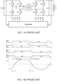
- FIGs. 1A and 1B respectively illustrate a typical isolated resonant converter topology and its ideal operating waveforms.
- the resonant components are a resonant inductor L R and a resonant capacitor C R .
- the circuit in FIG. 1A is referred to as a series-resonant converter (SRC).
- SRC series-resonant converter
- FIG. 1B illustrates typical timing diagrams of switch-control signals for the series-resonant converter (SRC) of FIG. 1A , operating with zero voltage switching (ZVS).
- SRC series-resonant converter
- ZVS zero voltage switching
- all switches S P1 , S P2 , S P3 , S P4 , S S1 , S S2 , S S3 , and S S4 operate with the same duty ratio of 50%, and the primary stage switches in the same leg (namely, S P1 , S P2 , and S P3 , S P4 ) operate in a complementary fashion to avoid cross-conduction.
- the frequency of primary switches is determined by a feedback control loop that is employed to regulate the output ("variable-frequency control").
- phase delay control operation of the secondary-side synchronous rectifier switches is realized by synchronizing their switching with zero crossing of a resonant current, i P . That is, a phase delay (e.g., T 0 to T 1 ) with respect to the waveforms for the primary stage switches (S P1 , S P2 , S P3 , and S P4 ) is introduced to the waveforms for the secondary stage switches (S S1 , S S2 , S S3 , and S S4 ).
- a phase delay e.g., T 0 to T 1
- switching of secondary-side synchronous rectifier switches S S1 and S S3 is synchronized with the positive period of resonant current, i P
- switching of secondary-side synchronous rectifier switches S S2 and S S4 is synchronized with the negative period of the resonant current, i P
- the duty ratios of primary switches are set to a value slightly less than 50% by introducing a short delay (or dead time) between the turn-off and turn-on of the complementarily operated same-leg switches.
- the current is commutated from the switch of the device that is turned off to the antiparallel diode of the other device which creates a condition for its subsequent ZVS turn on.
- the secondary-side synchronous rectifier switches are also operated with duty ratios slightly less than 50%.
- the series resonant converter with variable-frequency control as shown in FIG. 1A has a symmetric structure between the input and output ports, it is not suitable for bidirectional operation since it operates only as a step-down converter (i.e., V IN > (N 1 /N 2 ) ⁇ V o ).
- that implementation also makes the converter bidirectional, because the controllable switches on both sides of the transformer allow power to flow in both directions, and the proposed "delay time control" makes the series resonant converter capable of boosting the output voltage (i.e., (N 1 /N 2 ) ⁇ V o ⁇ V IN ).
- the switching-frequency-range reduction as well as the voltage step up/down operation are achieved by controlling the output with a combination of variable-frequency control and delay time control.
- the variable-frequency control is used to control primary switches, whereas the delay time control is employed to control the secondary-side rectifier switches.
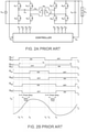
- FIGs. 2A and 2B respectively illustrates another typical isolated resonant converter topology and its ideal operating waveforms.
- the resonant components are a resonant inductor L R and a resonant capacitor C R .
- primary switches S P1 , S P2 , S P3 , and S P4 operate with the same switching frequency and have identical duty cycles of approximately 50%. To achieve zero-voltage-switching of the complementarily operated primary switches of the same leg, a small dead time is provided between the turn-on and turn-off instants of these complementary-operated switches.
- Secondary switches S S1 , S S2 , S S3 , and S S4 operate with the same switching frequency as the primary switches. However, secondary switches S S2 and S S3 operate with extended duty cycles that provide the delay time as shown in FIG. 2B . Secondary winding of transformer, TR, is shorted by secondary switches S S2 and S S3 during the delay time (for example, T 1 to T 2 and T 4 to T 5 ).
- the primary function of the delay time control is to make the series resonant converter be able to boost the output voltage so that it can reduce the switching frequency range of the converter.
- the voltage step up/down operation achieved by controlling the output with a combination of the variable-frequency control and the delay time control makes the converter suitable for applications that require the bidirectional power flow.
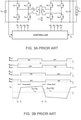
- FIGs. 3A and 3B respectively illustrate a circuit diagram of a DAB converter and its ideal operating waveforms.
- a DAB converter has a bidirectional converter topology.
- series inductor, L S is located between the primary-side active bridge that includes primary switches S P1 , S P2 , S P3 , and S P4 and the secondary-side active bridge that includes secondary switches S S1 , S S2 , S S3 , and S S4 .
- primary switches S P1 , S P2 , S P3 , and S P4 are operated with constant switching frequency.
- phase shift control is used to determine the amount of phase shift between the primary and secondary switching. As shown in FIG. 3B , all switches S P1 , S P2 , S P3 , S P4 , S S1 , S S2 , S S3 , and S S4 operate with the same switching frequency and have identical duty cycles of slightly less than 50%.
- the turn-on and turn-off moments of secondary switches S S1 , S S2 , S S3 , and S S4 are actively shifted (for example, from T 0 to T 1 , and from T 2 to T 3 ) from the turn-on and turn-off moments of primary switches S P1 , S P2 , S P3 , and S P4 as shown in FIG. 3B .
- the induced current, i P across the inductor, L S , is controlled.
- the DAB converter also works as a bidirectional converter because the controllable switches on both sides of the transformer allow power to flow in both directions, and the phase-shift control makes the converter operate in voltage step-up as well as step-down mode.
- various embodiments of a multiple-port bidirectional DC-DC converter and a control method therefor are disclosed, in which a single multiple-port bidirectional DC-DC converter can replace numerous unidirectional or bidirectional converters so that the total number of components is significantly reduced, and the utilization of components is improved.
- the present disclosure provides a multiple-port converter, comprising: a transformer having a primary winding, a secondary winding and a tertiary winding; a primary power stage having a first plurality of switches and electrically connected to a first energy source and the primary winding of the transformer; a secondary power stage having a second plurality of switches and electrically connected to a second energy source and the secondary winding of the transformer, the primary power stage and secondary power stage forming a series resonant converter; a tertiary power stage having a third plurality of switches and electrically connected to a third energy source and the tertiary winding of the transformer, the primary power stage and tertiary power stage forming a dual active bridge converter; and a controller electrically connected to the primary, secondary, and tertiary power stages to measure operating conditions in the multiple-port converter and to provide control signals to the first, second and third plurality of switches.
- the controller comprises control logic configured to send the control signals to the first and second plurality of switches to transfer energy between the first energy source and the second energy source using at least one of phase delay control and delay time control.
- the controller comprises control logic configured to send the control signals to the first, second, and third plurality of switches to transfer energy from the first energy source to the second energy source using phase delay control and to transfer energy from the first energy source to the third energy source using phase shift control.
- control logic of the controller is configured to vary a switching frequency of the control signals to modulate an amount of energy transferred to the secondary power stage, and wherein the phase shift control modulates an amount of energy transferred to the tertiary power stage.
- the switching frequency is the same for the primary, secondary, and tertiary power stages.
- the controller has control logic configured to send first and second control signals to the first plurality of switches and to send third and fourth control signals to the second plurality of switches, the third control signals are substantially identical to the first control signal with a phase delay, and the fourth control signals are substantially identical to the second control signal with the phase delay.
- the secondary power stage has a first capacitor and first inductor in series with the secondary winding of the transformer.
- the tertiary power stage has a second inductor in series with the tertiary winding of the transformer.
- the primary power stage has a second capacitor in series with the primary winding of the transformer
- the tertiary power stage has a third capacitor in series with the tertiary winding of the transformer.
- the controller comprises control logic configured to send the control signals to the first, second, and third plurality of switches to transfer energy from the second energy source to the first energy source using phase delay control and delay time control and to transfer energy from the first energy source to the third energy source using phase shift control.
- the tertiary power stage is a first tertiary power stage among a plurality of tertiary power stages, each of the plurality of tertiary power stages is connected to a respective winding of the transformer and to a respective energy source, and each tertiary power stage forms a respective dual active bridge converter with the primary power stage.
- the present disclosure provides a method of controlling a DC-DC converter having a plurality of stages including first, second and third stages, the method comprising acts of: measuring a plurality of electrical properties of the DC-DC converter; determining a switching frequency, phase delay, and phase shift based at least in part on the measured plurality of electrical properties; switching a first plurality of switches of the first stage at the switching frequency; switching at least two of a second plurality of switches of the second stage at the switching frequency, time shifted by the phase delay relative to switching of at least one of the first plurality of switches; and switching at least two of a third plurality of switches of the third stage at the switching frequency, time shifted by the phase shift relative to switching of a member of a group consisting of at least one of the first plurality of switches.
- the method further comprises acts of: determining a delay time based at least in part on the measured plurality of electrical properties; and switching at least two other of the second plurality of switches of the second stage at the switching frequency, time shifted by the delay time relative to switching of the at least two second switches.
- the measuring comprises measuring at least one of a group consisting of a voltage of an energy source connected to one of the plurality of stages and a current in one of the plurality of stages.
- the method further comprises an act of: electrically coupling the plurality of stages through a transformer having a first winding wired to the first stage, a second winding wired to the second stage, and a third winding wired to the third stage.
- a resonance frequency of the second stage is determined substantially by a second stage inductor and a second stage capacitor which are in series with the second winding of the transformer.
- the present disclosure provides a multiple-port converter, comprising: a transformer having a first winding, a second winding and a third winding; a series resonant converter formed by a first power stage and a second power stage; and a dual active bridge converter formed by the first power stage and a third power stage, wherein the first power stage is wired to the first winding, the second power stage is wired to the second winding, and the third power stage is wired to the third winding.
- the availability of redundant power systems with multiple energy sources can be maximized by providing multiple power paths.
- the high-availability system requires multiple bidirectional converters to charge and discharge between energy sources.
- employing multiple bidirectional converters for a system may not be cost effective. For example, to deliver energy among three energy sources in any direction, the system would require six unidirectional converters or three bidirectional converters.
- a new multiple-port (i.e., three or more ports) bidirectional DC-DC converter and a control method therefor are described. Such converters can be implemented cost effectively and with reduced size.
- FIG. 4 illustrates a three-port bidirectional DC-DC converter 400 in accordance with an embodiment of the present disclosure.
- the power stages of three-port bidirectional DC-DC converter 400 employ an isolation transformer 402 (or TR) with three windings and three power stages.
- converter 400 includes transformer 402 having first, second, and third windings 441, 442, and 443 respectively, magnetically coupled to each other (with or without a magnetic core), a first stage circuit 410 electrically coupled to first winding 441, a second stage circuit 420 electrically coupled to second winding 442, a third stage circuit 430 electrically coupled to third winding 443, and a controller 404 electrically coupled to first, second and third stage circuits 410, 420, and 430, so as to deliver energy and regulate downstream voltages or currents in any direction in converter 400.
- First winding 441 has N 1 turns
- second winding 442 has N 2 turns and third winding 443 and N 3 turns, where N 1 , N 2 and N 3 are positive integers.
- first stage circuit 410 is shown with a voltage source and second and third stage circuits 420 and 430 are shown with batteries, it should be appreciated that each stage circuit may be connected to any suitable energy source.
- stage circuits 410, 420, and 430 are electrically coupled to the respective windings of transformer 402 by wiring as shown in FIG. 4 .
- Controller 404 may also be electrically coupled by wiring to stage circuits 410, 420, and 430. Other forms of electrical coupling may be used in other embodiments.
- first stage circuit 410 of converter 400 comprises a plurality of switches S P1 , S P2 , S P3 , and S P4 and is coupled between an energy source V IN (e.g., a DC power source converted from a household AC power outlet) and first winding 441;
- second stage circuit 420 of converter 400 comprises a plurality of switches S S1 , S S2 , S S3 , and S S4 , a resonant capacitor, C R , and a resonant inductor, L R ;
- third stage circuit 430 comprises a plurality of switches S T1 , S T2 , S T3 , and S T4 and a series inductor, L T .
- Second stage circuit 420 is coupled between an energy source V B1 (e.g., a high voltage battery with an output voltage of about 250 to 500 Volts) and second winding 442, while third stage circuit 430 is coupled between an energy source V B2 (e.g., a low voltage battery with an output voltage of about 5 to 50 Volts) and third winding 443.
- the switches of the stage circuits may be implemented as MOSFETs, relays, bipolar junction transistors, Darlington transistors, or any suitable switching technology.
- First stage circuit 410 or third stage circuit 430 may be operated in combination with second stage circuit 420 as a series resonant converter. That is, topologically, the circuit formed by first stage circuit 410 and second stage circuit 420 (or second stage circuit 420 and third stage circuit 430) when the remaining stage circuit (i.e., third stage circuit 430, or first stage circuit 410, respectively) is ignored is a series resonant converter circuit.
- a series resonant converter is a converter with an associated resonance frequency determined by an effective capacitance and an effective inductance which are in series with one another. "Effective" is used here to refer to the lump element equivalent.
- a series resonant converter has a resonance frequency between about 40 kHz and 300 kHz (e.g., 80 kHz), though this range is exemplary and any suitable resonance frequency may be used.
- First stage circuit 410 and third stage circuit 430 may be operated in combination as a dual active bridge (DAB) converter. That is, topologically, the circuit formed by first stage circuit 410 and third stage circuit 430, when second stage circuit 420 is ignored is a DAB converter.
- a DAB converter is a converter with an effective series inductance between the two isolated switching stages. "Effective” is used here to refer to the lump element equivalent.
- the various inductors may be implemented as lumped elements, a network of lumped elements, as a distributed element (or “parasitic” effect) or any other suitable way or combination of ways.
- converter 400 allows for one of the series resonant converter topologies and the DAB converter topology to be operated simultaneously, and in some embodiments, in ways essentially identical, or quite similar to conventional operation of a series resonant converter and DAB converter. Still other modes of operation of converter 400 allow for power transfer between arbitrary ports of converter 400. Controls of converter 400 are further discussed in connection with controller 404 and FIGs. 5-16 .
- Controller 404 is used to measure the current conditions of converter 400 to facilitate controlled operation. Controller 404 may for example, include circuitry to measure voltage and current at various points in the converter circuit. Controller 404 includes control logic to implement variable-frequency control, phase-delay control, delay-time control, phase shift control, and other forms of control or combinations of control algorithms to control converter 400. Controller 404 may be implemented as a central processing unit (CPU), digital signal processor (DSP), general or special purpose microprocessor, microcontroller, field programmable gate array (FPGA), application-specific integrated circuit (ASIC) or any suitable device or combination of devices capable of controlling converter 400. In some embodiments, controller 404 may utilize an analog to digital converter (ADC) to sample signal levels and a pulse-width modulator (PWM) to control switching. Though, controller 404 may be implemented in any suitable way.
- ADC analog to digital converter
- PWM pulse-width modulator
- EMI electromagnetic interference
- converter 400 may deliver electrical energy from energy source V IN (first stage) to energy sources V B1 and V B2 (second and third stages) by a single controller 404 that independently controls charging currents to energy sources V B1 and V B2 .
- electrical energy of energy source V B1 (second stage) can be delivered to energy source V IN (first stage) and energy source V B2 (third stage).
- electrical energy of energy source V B2 (third stage) can be delivered to energy source V IN (first stage) and battery V B1 (second stage) by the independently controlled charging currents.
- Any stage i.e., any stage circuit and the corresponding energy source
- energy source V IN may be disconnected by opening switches S P1 , S P2 , S P3 , and S P4 and can be delivered from energy source V B1 to energy source V B2 , and vice versa. That is, three-port bidirectional DC-DC converter 400 as shown in FIG. 4 can deliver electrical energy and regulate downstream voltages or currents in any direction. To independently regulate voltages or currents of multiple outputs, a variable-frequency control, a delay time control, a phase-shift control, or the combination of two or three controls is employed.
- the three-port bidirectional DC-DC converter 400 substantially reduces the number of components that is needed to transfer electrical energy arbitrarily between stages when compared to conventional solutions which would require six unidirectional or three bidirectional converters such as the types shown in FIGs 1A , 2A , and 3A .
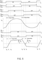
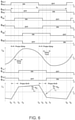
- FIGs. 5 and 6 illustrate switch activation control signal waveforms and the corresponding currents for three-port bidirectional DC-DC converter 400 of FIG. 4 .
- both FIGs. 5 and 6 illustrate power transfer from energy source V IN to energy sources V B1 and V B2 , in accordance with some embodiments of the present disclosure.
- first stage circuit 410 and second stage circuit 420 operate as a series resonant converter to transfer energy from V IN to V B1
- first stage circuit 410 and third stage circuit 430 operate as a DAB converter to transfer energy from V IN to V B2 .
- the voltage of energy source V IN is greater than n 1 times the voltage of energy source V B1 (i.e., V IN > n 1 V B1 ). In FIG. 6 , the voltage of energy source V IN is less than or equal to n 1 times the voltage of energy source V B1 (i.e., V IN ⁇ n 1 V B1 ).
- waveforms for the switches of first stage circuit 410 (S P1 through S P4 ), the switches of second stage circuit 420 (S S1 through S S4 ), and the switches of third stage circuit 430 (S T1 through S T4 ) are shown.
- Variable-frequency control is used to control the switching frequency of the switches S P1 through S P4 of first stage circuit 410.
- the switches of second and third stage circuit 420 and 430 operate at the same frequency as the switches of first stage circuit 410, and all the switches have identical duty cycles of approximately 50%.
- a small dead time is introduced between the turn-on and turn-off instants of the complementary-operated switches.
- the dead time may be one or more orders of magnitude shorter than the switching period (inverse of the switching frequency).
- switch S S2 is switched OFF slightly before switch S S1 is switched ON so that both switches in the S S1 and S S2 leg of the second stage circuit 420 are briefly simultaneously OFF.
- the variable-frequency control used to operate switches S P1 through S P4 of first stage circuit 410 induces the resonant current i S that determines a charge current I B1 of energy source V B1 .
- Phase delay control is used to operate switches S S1 through S S4 of second stage circuit 420 as synchronous rectifiers, i.e., switches S S1 and S S3 are turned ON when resonant current i S is positive (e.g., between time points T 1 and T 4 ), while switches S S2 and S S4 are turned ON when resonant current i S is negative (e.g., between time points T 4 and T 7 ).
- Phase shift control is used to control the turn ON and OFF moments of switches S T1 through S T4 of third stage circuit 430.
- the switching is synchronized with the addition of a phase shift from the turn ON and OFF moments of switches S P1 through S P4 of first stage circuit 410.
- the amount of phase shift (e.g., from time point T 0 to time point T 2 ) determines the magnitude of current i T which is proportional to the charge current I B2 of energy source V B2 .
- a delay time (e.g., from time point T 1 to time point T 3 ) is added to actively control switches S S1 through S S4 of second stage circuit 420.
- winding 442 of transformer 402 is shorted by switches S S1 and S S4 of second stage circuit 420, which boosts resonant current i S , as shown in FIG. 6 .
- charge current I B1 of energy source V B1 can be regulated not only by the switching frequency but also by the delay time.
- the primary function of the delay time control is to improve operating efficiency by reducing the control frequency range and/or increase the voltage gain of converter 400, because the magnitude of resonant current i S can also be controlled by the delay time.
- switches of second and third stage circuit 420 and 430 still operate at the same frequency as the switches of first stage circuit 410 (which are controlled by variable frequency control), and all switches have identical duty cycles of approximately 50%. Also, the introduction of delay time control in this configuration does not substantially alter the performance of the DAB converter transferring power from the first to third stages.
- the timing of switches S T1 through S T4 of third stage circuit 430 is with reference to the switches S P1 through S P4 of first stage circuit 410 and not the switches S S1 through S S4 of second stage circuit 420.
- FIG. 7 is a flow chart illustrating a method 700 for controlling converter 400 to transfer power from energy source V IN to energy sources V B1 and V B2 , in accordance with embodiments of the present disclosure.
- a first stage controller of controller 404 begins with sensing or estimating voltage and/or currents across or through various elements in converter 400.
- the specific voltages and currents to be sensed an estimated may depend on the specific techniques used to implement variable-frequency control, phase delay control, delay time control, and phase shift control.
- the voltages of energy source V IN and energy sources V B1 and V B2 , as well as currents i S , i T , I B1 , and I B2 may be measured or estimated. Any suitable technique may be used to measure or estimate the voltages and currents including indirect measurements.
- ADC analog to digital converter
- controller 404 determines the switching frequency for the variable-frequency control used to regulate current I B1 and/or the voltage of energy source V B1 .
- Any suitable approach to implementing variable-frequency control may be used to determine the switching frequency. See for example and not limitation, References [1], [2], and [4].
- variable-frequency control can be implemented in essentially the same ways it is implemented for conventional resonant converter topologies such as the circuits shown in FIGs 1A and 2A .
- phase delay needed for phase delay control is determined.
- the phase delay may be determined by detecting or estimating the zero-crossing moment of resonant current i S . This timing is used to determine the phase delay and thereby the turn ON and OFF time of switches S S1 -S S4 of second stage circuit 420 thereby calculating the phase delay.
- the phase delay time may be determined as the time between switching of a switch in the primary stage and the zero-crossing moment of resonant current i S .
- phase delay may be determined in any suitable way. For example and not limitation, see References [1] and [2].
- Step 740 the delay time needed to implement delay time control is determined.
- the delay time may be based on the voltages of energy sources V IN and V B1 as well as currents i S and I B1 , so as to achieve additional control of switches S S1 through S S4 of second stage circuit 420. It should be noted that the delay time is set to zero for the embodiment of FIG. 5 , while the delay time is added for the embodiment of FIG. 6 .
- delay-time control is implemented in ways similar to those described in Patent No. 9,490,704 , and References [1] and [2].
- the phase shift needed for phase shift control is determined so as to regulate current I B2 or the voltage of energy source V B2 .
- Phase shift control may be implemented in any suitable way. For example and not limitation, see References [3], [5], and [6].
- the phase shift is based on the voltage of energy source V IN , current I B2 , series inductance L T , and the switching frequency. Note that the phase shift in FIGs. 5 and 6 is relative to one or more of the switches in first stage circuit 410, which is the stage where power is originating.
- controller 404 updates the switching frequency, the phase delay, the delay time, and the phase shift. These may be implemented by writing in the appropriate value into corresponding pulse-width modulator (PWM) registers.
- PWM pulse-width modulator
- converter 400 may continue operation from the start.
- variable-frequency control, phase-delay control, delay-time control, and phase-shift control can continually adjust the timing of the control switches to achieve the needed power transfer efficiently.
- the method for controlling converter 400 includes combinations of the variable-frequency control, the delay time control, and the phase shift control.
- all switches operate with the same switching frequency and have identical duty ratios of approximately 50%.
- a small dead time is provided between the turn-on and turn-off instants of these switches.
- the variable-frequency control, the delay time control, the phase shift control, and/or a combination of two or three of these controls can be employed. For example, one can vary the switching frequency for all switches to adjust the charging current between first and second stage circuits 410 and 420. Further, while keeping the switching frequency the same, one can vary the phase shift for switches S T1 through S T4 to adjust the charging current between first and third stage circuits 410 and 430.
- method 700 will exclude certain steps or may perform the steps in a different order. As one example, some embodiments may skip step 740 for determining the delay time.
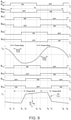
- FIGs. 8 and 9 illustrate switch activation control signal waveforms and the corresponding currents for power transfer from energy source V B1 to energy sources V IN and V B2 , in accordance with embodiments of the present disclosure.
- first stage circuit 410 and second stage circuit 420 operate as a series resonant converter to transfer energy from V B1 to V IN
- first stage circuit 410 and third stage circuit 430 operate as a DAB converter to transfer energy from V IN to V B2 .
- operationally energy is not directly transferred from V B1 to V B2 , but rather energy is transferred from V B1 to V IN and a portion of the energy delivered to V IN is delivered to V B2 .
- the voltage of energy source V B1 is greater than the voltage of energy source V IN divided by n 1 (i.e., V B1 > V IN /n 1 ).
- waveforms for the switches of first stage circuit 410 (S P1 through S P4 ), the switches of second stage circuit 420 (S S1 through S S4 ), and the switches of third stage circuit (S T1 through S T4 ) are shown.
- Variable-frequency control is used to control the switching frequency of the switches S S1 through S S4 of second stage circuit 420.
- the switches of first and third stage circuits 410 and 430 operate at the same frequency as the switches of second stage circuit 420, and all switches have identical duty cycles of approximately 50%.
- the variable-frequency control used to operate switches S S1 through S S4 of second stage circuit 420 induces the resonant current i S that determines a charge current I IN of energy source V IN .
- Phase delay control is used to operate switches S P1 through S P4 of first stage circuit 410 as synchronous rectifiers, i.e., switches S P2 and S P4 are turned ON when resonant current i S is positive (e.g., between time points T 4 and T 7 ), while switches S P1 and S P3 are turned ON when resonant current i S is negative (e.g., between time points T 1 and T 4 ).
- Phase shift control is used to control the turn ON and OFF moments of switches S T1 through S T4 of third stage circuit 430.
- the switching is synchronized with the addition of a phase shift with respect to the turn ON and OFF moments of switches S P1 through S P4 of first stage circuit 410.
- the amount of phase shift (e.g., from time point T 1 to time point T 2 ) determines the magnitude of current i T that is proportional to the charge current I B2 of energy source V B2 . It is important to emphasize here that the phase shift of the switches of third stage circuit 430 is relative to the switches of first stage circuit 410, not the switches of second stage circuit 420 from which transferred energy is originating. This is because of the choice to operate the first and second stage circuits 410 and 420 as a series resonant converter and to operate the first and third stage circuits 410 and 430 as a DAB converter.
- the voltage of energy source V B1 is less than or equal to the voltage of energy source V IN divided by n 1 (i.e., V BI ⁇ V IN / n 1 ).
- a delay time e.g., from time point T 1 to time point T 2
- first winding 441 of transformer 402 is shorted by the switches of first stage circuit 410, which boosts resonant current i S , as shown in FIG. 9 .
- charge current I IN of energy source V IN can be regulated not only by the switching frequency but also by the delay time.
- the switches of first and third stage circuits 410 and 430 still operate at the same frequency as the switches of second stage circuit 420 (which are controlled by variable frequency control) and all switches have identical duty cycles of approximately 50%.
- Phase shift control of the switches S T1 through S T4 of third stage circuit 430 is affected by the delay time control of the switches S P1 through S P4 of first stage circuit 410.
- the waveforms for switches S T1 and S T2 are essentially identical to switches S P1 and S P2 (i.e., S P1 , S P2 , S T1 and S T2 change states approximately at the zero crossings of i S ).
- Phase shift control of the switches of third stage circuit 430 causes a phase shift of switches S T3 and S T4 relative to the switches S P1 and S P2 of first stage circuit 410.
- the difference between the conventional phase shift control explained in FIGs. 5 , 6 and 8 versus the phase shift control in FIG. 9 is that in FIG. 9 , during the delay time control of the switches S P1 through S P4 of first stage circuit 410, the voltage across the inductor L T is zero.
- phase shift determines the magnitude of current i T which is proportional to charge current I B2 of energy source V B2 .
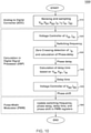
- FIG. 10 is a flow chart illustrating a method 1000 for controlling converter 400 to transfer power from energy source V B1 to energy sources V IN and V B2 , in accordance with some embodiments of the present disclosure. It should be appreciated that certain steps of method 1000 may be performed in ways similar to those described in connection with method 700 ( FIG. 7 ); though, method 1000 may be performed in any suitable way.
- controller 404 begins with sensing or estimating the voltages of energy sources V IN , V B1 and V B2 , as well as currents i S , i T , I B1 , and I B2 .
- controller 404 determines the switching frequency to regulate current I IN and/or the voltage of energy source V IN .
- Step 1030 the zero-crossing moment of resonant current i S is detected or estimated so as to determine the turn ON and OFF time of switches S P1 through S P4 of first stage circuit 410, thereby calculating the phase delay.
- Step 1040 the delay time is determined based on the voltages of energy sources V IN and V B1 as well as currents i S and I IN , so as to achieve additional control of switches S P1 through S P4 of first stage circuit 410. It should be noted that the delay time is set to zero for the embodiment of FIG. 8 , while the delay time is added for the embodiment of FIG. 9 .
- controller 404 determines the amount of phase shift to regulate current I B2 or the voltage of energy source V B2 .
- controller 404 updates the switching frequency, the phase delay, the delay time, and the phase shift in pulse-width modulator (PWM) registers, and converter 400 resumes its operation from the start.
- PWM pulse-width modulator
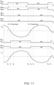
- FIGs. 11 and 12 illustrate switch activation control signal waveforms and the corresponding currents for power transfer from energy source V B1 to energy source V B2 , in accordance with embodiments of the present disclosure.
- energy source V IN is decoupled by turning off all of switches S P1 through S P4 of first stage circuit 410.
- second and third stage circuits 420 and 430 operate as a single input and single output converter. Specifically, the second and third stages act as a series resonant converter.
- the voltage of energy source V B1 is greater than n 3 times the voltage of energy source V B2 (i.e., V B1 > n 3 V B2 ).
- the voltage of energy source V B1 is less than or equal to n 3 times the voltage of energy source V B2 (i.e., V B1 ⁇ n 3 V B2 ).
- waveforms for switches S S1 through S S4 and switches S T1 through S T4 operate with the same switching frequency and have identical duty cycles of approximately 50%.
- the variable-frequency control is used to operate switches S S1 through S S4 of second stage circuit 420 and hence induces the resonant current i S and i T that determines a charge current I B2 of energy source V B2 .
- Switches S T1 through S T4 of third stage circuit 430 operate as synchronous rectifiers, i.e., switches S T1 and S T3 are turned ON when resonant current i T is positive (e.g., between time points T 1 and T 4 ), while switches S T2 and S T4 are turned ON when resonant current i T is negative (e.g., between time points T 4 and T 7 ).
- a delay time (e.g., from time point T 1 to time point T 2 ) is added to actively control switches S T1 through S T4 of third stage circuit 430.
- third winding 443 of transformer 402 is shorted by the switches of third stage circuit 430, which boosts resonant current i S and i T as shown in FIG. 12 .
- charge current I B2 of energy source V B2 can be regulated not only by the switching frequency but also by the delay time.
- FIG. 13 is a flow chart illustrating a method 1300 for controlling converter 400 to transfer power from energy source V B1 to energy source V B2 , in accordance with embodiments of the present disclosure.
- controller 404 begins with sensing or estimating the voltages of energy sources V B1 and V B2 , as well as currents i S and I B2 .
- controller 404 determines the switching frequency to regulate current I B2 and/or the voltage of energy source V B2 .
- Step 1330 the zero-crossing moment of resonant current i S is detected or estimated so as to determine the turn ON and OFF time of switches S T1 through S T4 of third stage circuit 430, thereby calculating the phase delay.
- the delay time is determined based on the voltages of energy sources V B1 and V B2 as well as current I B2 . It should be noted that the delay time is set to zero for the embodiment of FIG. 11 , while the delay time (e.g., between time points T 1 and T 2 ) is added for the embodiment of FIG. 12 .
- controller 404 turns off all of switches S P1 through S P4 of first stage circuit 410 and updates the switching frequency, the phase delay, the delay time, and the phase shift in pulse-width modulator (PWM) registers, and converter 400 resumes its operation from the start.
- PWM pulse-width modulator
- FIGs. 14 and 15 illustrate switch activation control signal waveforms and the corresponding currents for power transfer from energy source V B2 to energy source V B1 , in accordance with embodiments of the present disclosure.
- energy source V IN is decoupled by turning off all of switches S P1 through S P4 of first stage circuit 410. Accordingly, second and third stage circuits 420 and 430 operate as a single input and single output converter.
- the voltage of energy source V B2 is greater than (1/n 3 ) times the voltage of energy source V B .
- the voltage of energy source V B2 is less than or equal to (1/n 3 ) times the voltage of energy source V B1 .
- waveforms for switches S S1 through S S4 and switches S T1 through S T4 operate with the same switching frequency and have identical duty cycles of approximately 50%.
- the variable-frequency control is used to operate switches S S1 through S S4 of second stage circuit 420 and hence induces the resonant current i S and i T that determines a charge current I B1 of energy source V B1 .
- Switches S S1 through S S4 of second stage circuit 420 operate as synchronous rectifiers, i.e., switches S S1 and S S3 are turned ON when resonant current i S is positive (e.g., between time points T 1 and T 4 ), while switches S S2 and S S4 are turned ON when resonant current i S is negative (e.g., between time points T 4 and T 7 ).
- a delay time (e.g., from time point T 1 to time point T 2 ) is added to actively control switches S S3 and S S4 of second stage circuit 420.
- second winding 442 of transformer 402 is shorted by the switches of second stage circuit 420, which boosts resonant current i S and i T as shown in FIG. 15 .
- charge current I B1 of energy source V B1 can be regulated not only by the switching frequency but also by the delay time.
- FIG. 16 is a flow chart illustrating a method 1600 for controlling converter 400 to transfer power from energy source V B2 to energy source V B1 , in accordance with embodiments of the present disclosure.
- controller 404 begins with sensing or estimating the voltages of energy sources V B1 and V B2 , as well as currents i S and I B1 .
- controller 404 determines the switching frequency to regulate current I B1 and/or the voltage of energy source V B1 .
- Step 1630 the zero-crossing moment of resonant current i S is detected or estimated so as to determine the turn ON and OFF time of switches S S1 through S S4 of second stage circuit 420, thereby calculating the phase delay.
- Step 1640 the delay time is determined based on the voltages of energy sources V B1 and V B2 as well as current I B1 . It should be noted that the delay time is set to zero for the embodiment of FIG. 14 , while the delay time (e.g., between time points T 1 and T 2 ) is added for the embodiment of FIG. 15 .
- controller 404 turns off all of switches S P1 through S P4 of first stage circuit 410 and updates the switching frequency, the phase delay, the delay time, and the phase shift in pulse-width modulator (PWM) registers, and converter 400 resumes its operation from the start.
- PWM pulse-width modulator
- FIG. 17 illustrates a triple-port bidirectional DC-DC converter 1700 in accordance with another embodiment of the present disclosure.
- Converter 1700 in FIG. 17 is substantially the same as converter 400 in FIG. 4 , except that converter 1700 is implemented to include a blocking capacitor C B1 in first stage circuit 1710 and a blocking capacitor C B2 for third stage circuit 1730.
- blocking capacitors C B1 and C B2 are serially coupled to first winding 1741 and third winding 1743 of transformer 1702, respectively.
- Blocking capacitors C B1 and C B2 as well as resonant capacitor C R of second stage circuit 1720 can block any DC current through windings 1741, 1742, and 1743 and prevent saturation of transformer 1702. It is appreciated, however, that the capacitance of blocking capacitors C B1 and C B2 is much greater than that of resonant capacitor C R , such that resonant frequency of series resonant converter between second and first stage circuits 1720 and 1710 and resonant frequency of series resonant converter between second and third stage circuits 1720 and 1730 are approximately the same as that without the blocking capacitors.
- blocking capacitor C B2 may be omitted, namely only first power stage circuit 1710 has the blocking capacitor. Consequently, the circuit structure is simplified, or the cost is reduced.
- the uneven duty-cycles of the switches are caused by the uneven delays of the gate drive signals and unequal turn-on and turn-off delays of the switches. If the mismatch of the delays is well minimized by an optimized design procedure, saturation of a transformer can be prevented by designing a transformer with a relatively large air gap without blocking capacitors as shown in FIG. 4 .
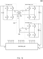
- FIG. 18 illustrates a triple-port bidirectional DC-DC converter 1800 in accordance with yet another embodiment of the present disclosure.
- Converter 1800 in FIG. 18 is substantially the same as converter 1700 in FIG. 17 , except that inductors L R and L T originally included respectively in second and third stage circuits 1720 and 1730 of FIG. 17 are now magnetically integrated into transformer 1802 of FIG. 18 .
- inductors L R and L T originally included respectively in second and third stage circuits 1720 and 1730 of FIG. 17 are now magnetically integrated into transformer 1802 of FIG. 18 .
- windings 1841, 1842, and 1843 of transformer 1802 e.g., by leaving a space/gap between neighboring turns of windings N 1 , N 2 , and N 3
- leakage inductances of these windings can be determined and perform as series connected inductors L R and L T .
- the leakage inductance of first winding 1841 is minimized in comparison with the leakage inductances of second and third wind
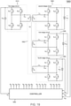
- FIG. 19 illustrates a quadruple-port bidirectional DC-DC converter 1900, in accordance with an embodiment of the present disclosure.
- converter 1900 includes four converter stages (i.e., a first stage circuit 1910, a second stage circuit 1920, a third stage circuit 1930 and a fourth stage circuit 1940) magnetically coupled to each other through transformer 1902 and individually controllable by controller 1904.
- first, third and fourth stage circuits 1910, 1930, and 1940 can optionally include a blocking capacitor
- second stage circuit 1920 includes a resonant capacitor having a much smaller capacitance than the blocking capacitor.
- FIG. 20 illustrates a multiple-port bidirectional DC-DC converter 2000, in accordance with an embodiment of the present disclosure.
- converter 2000 is generalized to include N stage circuits.
- Each of the N stage circuits can optionally include a blocking capacitor except the second stage circuit which instead includes a resonant capacitor having a much smaller capacitance than the blocking capacitor.
- only one of the stage circuits is configured to transfer electric energy as an SRC, while the remaining stage circuits are configured to transfer energy as a DAB.
- phase shift control may be used for each DAB and the amount of phase shift may be determined independently for each.
Landscapes
- Engineering & Computer Science (AREA)
- Power Engineering (AREA)
- Computer Networks & Wireless Communication (AREA)
- Dc-Dc Converters (AREA)
- Charge And Discharge Circuits For Batteries Or The Like (AREA)
- Control Of Eletrric Generators (AREA)
- Electrophonic Musical Instruments (AREA)
Abstract
Description
- The present disclosure relates to a multiple-port bidirectional DC-DC converter and a control method thereof. More particularly, the present disclosure relates to an integrated one or more bidirectional resonant converters and one or more dual active bridge (DAB) converters with bidirectional control.
- High-availability power systems for equipment used in mission-critical applications must be implemented with enhanced reliability. Usually, increased power-system reliability is achieved by employing power system components with high intrinsic reliability and by implementing highly redundant power-system architectures that include the redundancy of energy sources. The energy source generally consists of an ac utility line, stacks of batteries with or without downstream loads, or super capacitors. The availability of redundant power systems with multiple energy sources can be maximized by providing multiple power paths. In applications with more than one energy source, all energy sources are charged by a single source while each energy source is coupled to its individual load to deliver uninterrupted power. However, to increase reliability, one of the energy sources should be able to deliver energy to the other energy sources and vice versa. As a result, the high-availability system requires multiple bidirectional converters to charge and discharge between energy sources. There are known bidirectional converters with series resonant converter topologies and dual active bridge (DAB) converter topologies.
- Generally, resonant converters employ a resonant-tank circuit to shape the switch voltage and/or current waveforms to minimize switching losses and allow high-frequency operation without deterioration of conversion efficiency. Moreover, because resonant converters absorb parasitic components such as leakage and/or magnetizing inductance of transformers into their resonant-tank circuit, they are inevitably used in applications where these parasitic components are pronounced, such as high-voltage and/or high-current isolated power supplies for battery charging systems.
-
FIGs. 1A and 1B respectively illustrate a typical isolated resonant converter topology and its ideal operating waveforms. As shown inFIG. 1A , in this topology, the resonant components are a resonant inductor LR and a resonant capacitor CR. Because resonant inductor LR is connected in series with resonant capacitors CR, the circuit inFIG. 1A is referred to as a series-resonant converter (SRC). It should be noted that to maximize conversion efficiency, the secondary-side diode rectifiers are usually implemented by synchronous rectifiers. -
FIG. 1B illustrates typical timing diagrams of switch-control signals for the series-resonant converter (SRC) ofFIG. 1A , operating with zero voltage switching (ZVS). Referring to bothFIGs. 1A and 1B , all switches SP1, SP2, SP3, SP4, SS1, SS2, SS3, and SS4 operate with the same duty ratio of 50%, and the primary stage switches in the same leg (namely, SP1, SP2, and SP3, SP4) operate in a complementary fashion to avoid cross-conduction. The frequency of primary switches is determined by a feedback control loop that is employed to regulate the output ("variable-frequency control"). The phase delay control operation of the secondary-side synchronous rectifier switches is realized by synchronizing their switching with zero crossing of a resonant current, iP. That is, a phase delay (e.g., T0 to T1) with respect to the waveforms for the primary stage switches (SP1, SP2, SP3, and SP4) is introduced to the waveforms for the secondary stage switches (SS1, SS2, SS3, and SS4). - Specifically, as shown in
FIG. 1B , switching of secondary-side synchronous rectifier switches SS1 and SS3 is synchronized with the positive period of resonant current, iP, whereas switching of secondary-side synchronous rectifier switches SS2 and SS4 is synchronized with the negative period of the resonant current, iP. To achieve ZVS in practical implementations, the duty ratios of primary switches are set to a value slightly less than 50% by introducing a short delay (or dead time) between the turn-off and turn-on of the complementarily operated same-leg switches. During this dead time, the current is commutated from the switch of the device that is turned off to the antiparallel diode of the other device which creates a condition for its subsequent ZVS turn on. The secondary-side synchronous rectifier switches are also operated with duty ratios slightly less than 50%. Although the series resonant converter with variable-frequency control as shown inFIG. 1A has a symmetric structure between the input and output ports, it is not suitable for bidirectional operation since it operates only as a step-down converter (i.e., VIN > (N1/N2)·Vo). - For example,
U.S. Patent No. 9,490,704 to Jang and Jovanović issued November 8, 2016 -
FIGs. 2A and 2B , respectively illustrates another typical isolated resonant converter topology and its ideal operating waveforms. As shown inFIG. 2A , in this topology, the resonant components are a resonant inductor LR and a resonant capacitor CR. As shown inFIG. 2B , primary switches SP1, SP2, SP3, and SP4 operate with the same switching frequency and have identical duty cycles of approximately 50%. To achieve zero-voltage-switching of the complementarily operated primary switches of the same leg, a small dead time is provided between the turn-on and turn-off instants of these complementary-operated switches. Secondary switches SS1, SS2, SS3, and SS4 operate with the same switching frequency as the primary switches. However, secondary switches SS2 and SS3 operate with extended duty cycles that provide the delay time as shown inFIG. 2B . Secondary winding of transformer, TR, is shorted by secondary switches SS2 and SS3 during the delay time (for example, T1 to T2 and T4 to T5). The primary function of the delay time control is to make the series resonant converter be able to boost the output voltage so that it can reduce the switching frequency range of the converter. Moreover, the voltage step up/down operation achieved by controlling the output with a combination of the variable-frequency control and the delay time control makes the converter suitable for applications that require the bidirectional power flow. -
FIGs. 3A and 3B respectively illustrate a circuit diagram of a DAB converter and its ideal operating waveforms. It is well-known in the art that a DAB converter has a bidirectional converter topology. As shown inFIG. 3A , in this topology, series inductor, LS, is located between the primary-side active bridge that includes primary switches SP1, SP2, SP3, and SP4 and the secondary-side active bridge that includes secondary switches SS1, SS2, SS3, and SS4. Typically, primary switches SP1, SP2, SP3, and SP4 are operated with constant switching frequency. This switching frequency is matched by the secondary switches SS1, SS2, SS3, and SS4. Additionally, phase shift control is used to determine the amount of phase shift between the primary and secondary switching. As shown inFIG. 3B , all switches SP1, SP2, SP3, SP4, SS1, SS2, SS3, and SS4 operate with the same switching frequency and have identical duty cycles of slightly less than 50%. It should be noted that the turn-on and turn-off moments of secondary switches SS1, SS2, SS3, and SS4 are actively shifted (for example, from T0 to T1, and from T2 to T3) from the turn-on and turn-off moments of primary switches SP1, SP2, SP3, and SP4 as shown inFIG. 3B . By actively shifting the gate signals of the secondary switches, the induced current, iP, across the inductor, LS, is controlled. The DAB converter also works as a bidirectional converter because the controllable switches on both sides of the transformer allow power to flow in both directions, and the phase-shift control makes the converter operate in voltage step-up as well as step-down mode. - The following references, incorporated herein by reference, provide some additional background in the technical field:
- [1] G. Liu, Y. Jang, M. M. Jovanović and J. Q. Zhang, "Implementation of a 3.3-kW DC-DC Converter for EV On-Board Charger Employing the Series-Resonant Converter With Reduced-Frequency-Range Control," in IEEE Transactions on Power Electronics, vol. 32, no. 6, pp. 4168-4184, June 2017, doi: 10.1109/TPEL.2016.2598173.
- [2] Y. Jang, M. M. Jovanovic, M. Kumar, J. M. Ruiz, R. Lu and T. Wei, "Isolated, Bi-Directional DC-DC Converter for Fuel Cell Electric Vehicle Applications," 2019 IEEE Applied Power Electronics Conference and Exposition (APEC), Anaheim, CA, USA, 2019, pp. 1674-1681, doi: 10.1109/APEC.2019.8722067.
- [3] G. G. Oggier, R. Leidhold, G. O. Garcia, A. R. Oliva, J. C. Balda and F. Barlow, "Extending the ZVS operating range of dual active bridge high-power DC-DC converters," 2006 37th IEEE Power Electronics Specialists Conference, Jeju, 2006, pp. 1-7, doi: 10.1109/pesc.2006.1712142.
- [4] M. M. Jovanović (1994) Invited paper. "Resonant, quasi-resonant, multi-resonant and soft-switching techniques-merits and limitations," International Journal of Electronics, 77:5, 537-554, DOI: 10.1080/00207219408926086
- [5] M. N. Kheraluwala, R. W. Gascoigne, D. M. Divan and E. D. Baumann, "Performance characterization of a high-power dual active bridge DC-to-DC converter," in IEEE Transactions on Industry Applications, vol. 28, no. 6, pp. 1294-1301, Nov.-Dec. 1992, doi: 10.1109/28.175280.
- [6]
A. K. Jain, R. Ayyanar, (Nov. 19, 2013). U.S. Patent No. 8,587,975 . - In the present disclosure, various embodiments of a multiple-port bidirectional DC-DC converter and a control method therefor are disclosed, in which a single multiple-port bidirectional DC-DC converter can replace numerous unidirectional or bidirectional converters so that the total number of components is significantly reduced, and the utilization of components is improved.
- In one aspect, the present disclosure provides a multiple-port converter, comprising: a transformer having a primary winding, a secondary winding and a tertiary winding; a primary power stage having a first plurality of switches and electrically connected to a first energy source and the primary winding of the transformer; a secondary power stage having a second plurality of switches and electrically connected to a second energy source and the secondary winding of the transformer, the primary power stage and secondary power stage forming a series resonant converter; a tertiary power stage having a third plurality of switches and electrically connected to a third energy source and the tertiary winding of the transformer, the primary power stage and tertiary power stage forming a dual active bridge converter; and a controller electrically connected to the primary, secondary, and tertiary power stages to measure operating conditions in the multiple-port converter and to provide control signals to the first, second and third plurality of switches.
- In one embodiment, the controller comprises control logic configured to send the control signals to the first and second plurality of switches to transfer energy between the first energy source and the second energy source using at least one of phase delay control and delay time control.
- In one embodiment, the controller comprises control logic configured to send the control signals to the first, second, and third plurality of switches to transfer energy from the first energy source to the second energy source using phase delay control and to transfer energy from the first energy source to the third energy source using phase shift control.
- In one embodiment, the control logic of the controller is configured to vary a switching frequency of the control signals to modulate an amount of energy transferred to the secondary power stage, and wherein the phase shift control modulates an amount of energy transferred to the tertiary power stage.
- In one embodiment, the switching frequency is the same for the primary, secondary, and tertiary power stages.
- In one embodiment, the controller has control logic configured to send first and second control signals to the first plurality of switches and to send third and fourth control signals to the second plurality of switches, the third control signals are substantially identical to the first control signal with a phase delay, and the fourth control signals are substantially identical to the second control signal with the phase delay.
- In one embodiment, the secondary power stage has a first capacitor and first inductor in series with the secondary winding of the transformer.
- In one embodiment, the tertiary power stage has a second inductor in series with the tertiary winding of the transformer.
- In one embodiment, the primary power stage has a second capacitor in series with the primary winding of the transformer, and the tertiary power stage has a third capacitor in series with the tertiary winding of the transformer.
- In one embodiment, the controller comprises control logic configured to send the control signals to the first, second, and third plurality of switches to transfer energy from the second energy source to the first energy source using phase delay control and delay time control and to transfer energy from the first energy source to the third energy source using phase shift control.
- In one embodiment, the tertiary power stage is a first tertiary power stage among a plurality of tertiary power stages, each of the plurality of tertiary power stages is connected to a respective winding of the transformer and to a respective energy source, and each tertiary power stage forms a respective dual active bridge converter with the primary power stage.
- In another aspect, the present disclosure provides a method of controlling a DC-DC converter having a plurality of stages including first, second and third stages, the method comprising acts of: measuring a plurality of electrical properties of the DC-DC converter; determining a switching frequency, phase delay, and phase shift based at least in part on the measured plurality of electrical properties; switching a first plurality of switches of the first stage at the switching frequency; switching at least two of a second plurality of switches of the second stage at the switching frequency, time shifted by the phase delay relative to switching of at least one of the first plurality of switches; and switching at least two of a third plurality of switches of the third stage at the switching frequency, time shifted by the phase shift relative to switching of a member of a group consisting of at least one of the first plurality of switches.
- In one embodiment, the method further comprises acts of: determining a delay time based at least in part on the measured plurality of electrical properties; and switching at least two other of the second plurality of switches of the second stage at the switching frequency, time shifted by the delay time relative to switching of the at least two second switches.
- In one embodiment, the measuring comprises measuring at least one of a group consisting of a voltage of an energy source connected to one of the plurality of stages and a current in one of the plurality of stages.
- In one embodiment, the method further comprises an act of: electrically coupling the plurality of stages through a transformer having a first winding wired to the first stage, a second winding wired to the second stage, and a third winding wired to the third stage.
- In one embodiment, a resonance frequency of the second stage is determined substantially by a second stage inductor and a second stage capacitor which are in series with the second winding of the transformer.
- In still another aspect, the present disclosure provides a multiple-port converter, comprising: a transformer having a first winding, a second winding and a third winding; a series resonant converter formed by a first power stage and a second power stage; and a dual active bridge converter formed by the first power stage and a third power stage, wherein the first power stage is wired to the first winding, the second power stage is wired to the second winding, and the third power stage is wired to the third winding.
-
-
FIGs. 1A and 1B respectively illustrate a typical isolated resonant converter topology and its ideal operating waveforms; -
FIGs. 2A and 2B , respectively illustrates another typical isolated resonant converter topology and its ideal operating waveforms; -
FIGs. 3A and 3B respectively illustrate a circuit diagram of a DAB converter and its ideal operating waveforms; -
FIG. 4 illustrates a three-port bidirectional DC-DC converter, in accordance with an embodiment of the present disclosure; -
FIGs. 5 and6 illustrate switch activation control signal waveforms and the corresponding currents for power transfer from energy source VIN to energy sources VB1 and VB2, in accordance with embodiments of the present disclosure; -
FIG. 7 is a flow chart illustrating a method for controlling a converter to transfer power from energy source VIN to energy sources VB1 and VB2, in accordance with embodiments of the present disclosure; -
FIGs. 8 and9 illustrate switch activation control signal waveforms and the corresponding currents for power transfer from energy source VB1 to energy sources VIN and VB2, in accordance with embodiments of the present disclosure; -
FIG. 10 is a flow chart illustrating a method for controlling a converter to transfer power from energy source VB1 to energy sources VIN and VB2, in accordance with embodiments of the present disclosure; -
FIGs. 11 and12 illustrate switch activation control signal waveforms and the corresponding currents for power transfer from energy source VB1 to energy source VB2, in accordance with embodiments of the present disclosure; -
FIG. 13 is a flow chart illustrating a method for controlling converter to transfer power from energy source VB1 to energy source VB2, in accordance with embodiments of the present disclosure; -
FIGs. 14 and15 illustrate switch activation control signal waveforms and the corresponding currents for power transfer from energy source VB2 to energy source VB1, in accordance with embodiments of the present disclosure; -
FIG. 16 is a flow chart illustrating a method for controlling a converter to transfer power from energy source VB2 to energy source VB1, in accordance with embodiments of the present disclosure; -
FIG. 17 illustrates a triple-port bidirectional DC-DC converter, in accordance with another embodiment of the present disclosure; -
FIG. 18 illustrates a triple-port bidirectional DC-DC converter, in accordance with yet another embodiment of the present disclosure; -
FIG. 19 illustrates a quadruple-port bidirectional DC-DC converter, in accordance with an embodiment of the present disclosure; and -
FIG. 20 illustrates a multiple-port bidirectional DC-DC converter 2000, in accordance with an embodiment of the present disclosure. - The present disclosure will now be described more specifically with reference to the following embodiments. It is to be noted that the following descriptions of preferred embodiments of this disclosure are presented herein for purpose of illustration and description only. It is not intended to be exhaustive or to be limited to the precise form disclosed.
- The availability of redundant power systems with multiple energy sources can be maximized by providing multiple power paths. As a result, the high-availability system requires multiple bidirectional converters to charge and discharge between energy sources. However, employing multiple bidirectional converters for a system may not be cost effective. For example, to deliver energy among three energy sources in any direction, the system would require six unidirectional converters or three bidirectional converters. A new multiple-port (i.e., three or more ports) bidirectional DC-DC converter and a control method therefor are described. Such converters can be implemented cost effectively and with reduced size.
-
FIG. 4 illustrates a three-port bidirectional DC-DC converter 400 in accordance with an embodiment of the present disclosure. As shown inFIG. 4 , the power stages of three-port bidirectional DC-DC converter 400 employ an isolation transformer 402 (or TR) with three windings and three power stages. Specifically,converter 400 includestransformer 402 having first, second, andthird windings first stage circuit 410 electrically coupled to first winding 441, asecond stage circuit 420 electrically coupled to second winding 442, athird stage circuit 430 electrically coupled to third winding 443, and acontroller 404 electrically coupled to first, second andthird stage circuits converter 400. First winding 441 has N1 turns, second winding 442 has N2 turns and third winding 443 and N3 turns, where N1, N2 and N3 are positive integers. The ratio of N1 to N2 is defined as n1 (i.e., n1 = N1/N2), the ratio of N1 to N3 is defined as n2 (i.e., n2 = N1/N3), and the ratio of N2 to N3 is defined as n3 (i.e., n3 = N2/N3). Whilefirst stage circuit 410 is shown with a voltage source and second andthird stage circuits stage circuits transformer 402 by wiring as shown inFIG. 4 .Controller 404 may also be electrically coupled by wiring to stagecircuits - In one embodiment,
first stage circuit 410 ofconverter 400 comprises a plurality of switches SP1, SP2, SP3, and SP4 and is coupled between an energy source VIN (e.g., a DC power source converted from a household AC power outlet) and first winding 441;second stage circuit 420 ofconverter 400 comprises a plurality of switches SS1, SS2, SS3, and SS4, a resonant capacitor, CR, and a resonant inductor, LR; andthird stage circuit 430 comprises a plurality of switches ST1, ST2, ST3, and ST4 and a series inductor, LT.Second stage circuit 420 is coupled between an energy source VB1 (e.g., a high voltage battery with an output voltage of about 250 to 500 Volts) and second winding 442, whilethird stage circuit 430 is coupled between an energy source VB2 (e.g., a low voltage battery with an output voltage of about 5 to 50 Volts) and third winding 443. Resonant capacitor, CR, and a resonant inductor, LR, may have a resonant frequency associated therewith which may be computed in radians as the inverse of the square root of the product of the capacitance and inductance in SI units (i.e.,
-
First stage circuit 410 orthird stage circuit 430 may be operated in combination withsecond stage circuit 420 as a series resonant converter. That is, topologically, the circuit formed byfirst stage circuit 410 and second stage circuit 420 (orsecond stage circuit 420 and third stage circuit 430) when the remaining stage circuit (i.e.,third stage circuit 430, orfirst stage circuit 410, respectively) is ignored is a series resonant converter circuit. A series resonant converter is a converter with an associated resonance frequency determined by an effective capacitance and an effective inductance which are in series with one another. "Effective" is used here to refer to the lump element equivalent. The various inductors and capacitors may be implemented as lumped elements, a network of lumped elements, as a distributed element (or "parasitic" effect) or any other suitable way or combination of ways. In some embodiments, a series resonant converter has a resonance frequency between about 40 kHz and 300 kHz (e.g., 80 kHz), though this range is exemplary and any suitable resonance frequency may be used. -
First stage circuit 410 andthird stage circuit 430 may be operated in combination as a dual active bridge (DAB) converter. That is, topologically, the circuit formed byfirst stage circuit 410 andthird stage circuit 430, whensecond stage circuit 420 is ignored is a DAB converter. A DAB converter is a converter with an effective series inductance between the two isolated switching stages. "Effective" is used here to refer to the lump element equivalent. The various inductors may be implemented as lumped elements, a network of lumped elements, as a distributed element (or "parasitic" effect) or any other suitable way or combination of ways. - Advantageously,
converter 400 allows for one of the series resonant converter topologies and the DAB converter topology to be operated simultaneously, and in some embodiments, in ways essentially identical, or quite similar to conventional operation of a series resonant converter and DAB converter. Still other modes of operation ofconverter 400 allow for power transfer between arbitrary ports ofconverter 400. Controls ofconverter 400 are further discussed in connection withcontroller 404 andFIGs. 5-16 . -
Controller 404 is used to measure the current conditions ofconverter 400 to facilitate controlled operation.Controller 404 may for example, include circuitry to measure voltage and current at various points in the converter circuit.Controller 404 includes control logic to implement variable-frequency control, phase-delay control, delay-time control, phase shift control, and other forms of control or combinations of control algorithms to controlconverter 400.Controller 404 may be implemented as a central processing unit (CPU), digital signal processor (DSP), general or special purpose microprocessor, microcontroller, field programmable gate array (FPGA), application-specific integrated circuit (ASIC) or any suitable device or combination of devices capable of controllingconverter 400. In some embodiments,controller 404 may utilize an analog to digital converter (ADC) to sample signal levels and a pulse-width modulator (PWM) to control switching. Though,controller 404 may be implemented in any suitable way. - It should be noted that in some implementations, it may be necessary to couple an electromagnetic interference (EMI) filter between each energy source and each power stage of
converter 400. Since the EMI filters are irrelevant to the converter operation of the present disclosure, such filters are not shown inFIG. 4 so as to simplify the drawings and the related discussions. - In one embodiment,
converter 400 may deliver electrical energy from energy source VIN (first stage) to energy sources VB1 and VB2 (second and third stages) by asingle controller 404 that independently controls charging currents to energy sources VB1 and VB2. Likewise, electrical energy of energy source VB1 (second stage) can be delivered to energy source VIN (first stage) and energy source VB2 (third stage). Likewise, electrical energy of energy source VB2 (third stage) can be delivered to energy source VIN (first stage) and battery VB1 (second stage) by the independently controlled charging currents. Any stage (i.e., any stage circuit and the corresponding energy source) can be effectively disconnected from power transfer by opening all its respective switches while electrical energy is transferred between the remaining two ports. For example, energy source VIN may be disconnected by opening switches SP1, SP2, SP3, and SP4 and can be delivered from energy source VB1 to energy source VB2, and vice versa. That is, three-port bidirectional DC-DC converter 400 as shown inFIG. 4 can deliver electrical energy and regulate downstream voltages or currents in any direction. To independently regulate voltages or currents of multiple outputs, a variable-frequency control, a delay time control, a phase-shift control, or the combination of two or three controls is employed. - It should be appreciated that the three-port bidirectional DC-
DC converter 400 substantially reduces the number of components that is needed to transfer electrical energy arbitrarily between stages when compared to conventional solutions which would require six unidirectional or three bidirectional converters such as the types shown inFIGs 1A ,2A , and3A . -
FIGs. 5 and6 illustrate switch activation control signal waveforms and the corresponding currents for three-port bidirectional DC-DC converter 400 ofFIG. 4 . Specifically, bothFIGs. 5 and6 illustrate power transfer from energy source VIN to energy sources VB1 and VB2, in accordance with some embodiments of the present disclosure. In this type of operationsfirst stage circuit 410 andsecond stage circuit 420 operate as a series resonant converter to transfer energy from VIN to VB1, andfirst stage circuit 410 andthird stage circuit 430 operate as a DAB converter to transfer energy from VIN to VB2. InFIG. 5 , the voltage of energy source VIN is greater than n1 times the voltage of energy source VB1 (i.e., VIN > n1VB1). InFIG. 6 , the voltage of energy source VIN is less than or equal to n1 times the voltage of energy source VB1 (i.e., VIN ≤ n1VB1). - Referring to
FIG. 5 , waveforms for the switches of first stage circuit 410 (SP1 through SP4), the switches of second stage circuit 420 (SS1 through SS4), and the switches of third stage circuit 430 (ST1 through ST4) are shown. Variable-frequency control is used to control the switching frequency of the switches SP1 through SP4 offirst stage circuit 410. The switches of second andthird stage circuit first stage circuit 410, and all the switches have identical duty cycles of approximately 50%. To achieve zero-voltage-switching (e.g., current iS = 0 at time point T1) of the complementary-operated switches of the same leg, a small dead time is introduced between the turn-on and turn-off instants of the complementary-operated switches. In some embodiments, the dead time may be one or more orders of magnitude shorter than the switching period (inverse of the switching frequency). For example, at time T1, switch SS2 is switched OFF slightly before switch SS1 is switched ON so that both switches in the SS1 and SS2 leg of thesecond stage circuit 420 are briefly simultaneously OFF. The variable-frequency control used to operate switches SP1 through SP4 offirst stage circuit 410 induces the resonant current iS that determines a charge current IB1 of energy source VB1. - Phase delay control is used to operate switches SS1 through SS4 of
second stage circuit 420 as synchronous rectifiers, i.e., switches SS1 and SS3 are turned ON when resonant current iS is positive (e.g., between time points T1 and T4), while switches SS2 and SS4 are turned ON when resonant current iS is negative (e.g., between time points T4 and T7). This effectively introduces a phase delay (e.g., from time point T0 to time point T1) to the waveforms for switches SS1 through SS4 with respect to the waveforms for switches SP1 through SP4. - Phase shift control is used to control the turn ON and OFF moments of switches ST1 through ST4 of
third stage circuit 430. The switching is synchronized with the addition of a phase shift from the turn ON and OFF moments of switches SP1 through SP4 offirst stage circuit 410. The amount of phase shift (e.g., from time point T0 to time point T2) determines the magnitude of current iT which is proportional to the charge current IB2 of energy source VB2. - Referring to
FIG. 6 , a delay time (e.g., from time point T1 to time point T3) is added to actively control switches SS1 through SS4 ofsecond stage circuit 420. During the delay time, winding 442 oftransformer 402 is shorted by switches SS1 and SS4 ofsecond stage circuit 420, which boosts resonant current iS, as shown inFIG. 6 . As a result, charge current IB1 of energy source VB1 can be regulated not only by the switching frequency but also by the delay time. The primary function of the delay time control is to improve operating efficiency by reducing the control frequency range and/or increase the voltage gain ofconverter 400, because the magnitude of resonant current iS can also be controlled by the delay time. Note that the switches of second andthird stage circuit third stage circuit 430 is with reference to the switches SP1 through SP4 offirst stage circuit 410 and not the switches SS1 through SS4 ofsecond stage circuit 420. -
FIG. 7 is a flow chart illustrating amethod 700 for controllingconverter 400 to transfer power from energy source VIN to energy sources VB1 and VB2, in accordance with embodiments of the present disclosure. - In
Step 710, a first stage controller ofcontroller 404 begins with sensing or estimating voltage and/or currents across or through various elements inconverter 400. The specific voltages and currents to be sensed an estimated may depend on the specific techniques used to implement variable-frequency control, phase delay control, delay time control, and phase shift control. For example, the voltages of energy source VIN and energy sources VB1 and VB2, as well as currents iS, iT, IB1, and IB2 may be measured or estimated. Any suitable technique may be used to measure or estimate the voltages and currents including indirect measurements. For example, an analog to digital converter (ADC) may be used. - In
Step 720,controller 404 determines the switching frequency for the variable-frequency control used to regulate current IB1 and/or the voltage of energy source VB1. Any suitable approach to implementing variable-frequency control may be used to determine the switching frequency. See for example and not limitation, References [1], [2], and [4]. In some embodiments of the disclosure, variable-frequency control can be implemented in essentially the same ways it is implemented for conventional resonant converter topologies such as the circuits shown inFIGs 1A and2A . - In
Step 730, the phase delay needed for phase delay control is determined. The phase delay may be determined by detecting or estimating the zero-crossing moment of resonant current iS. This timing is used to determine the phase delay and thereby the turn ON and OFF time of switches SS1-SS4 ofsecond stage circuit 420 thereby calculating the phase delay. The phase delay time may be determined as the time between switching of a switch in the primary stage and the zero-crossing moment of resonant current iS. Though, phase delay may be determined in any suitable way. For example and not limitation, see References [1] and [2]. - In
Step 740, the delay time needed to implement delay time control is determined. The delay time may be based on the voltages of energy sources VIN and VB1 as well as currents iS and IB1, so as to achieve additional control of switches SS1 through SS4 ofsecond stage circuit 420. It should be noted that the delay time is set to zero for the embodiment ofFIG. 5 , while the delay time is added for the embodiment ofFIG. 6 . In some embodiments of the disclosure, delay-time control is implemented in ways similar to those described in Patent No.9,490,704 - In
Step 750, the phase shift needed for phase shift control is determined so as to regulate current IB2 or the voltage of energy source VB2. Phase shift control may be implemented in any suitable way. For example and not limitation, see References [3], [5], and [6]. In some embodiments, the phase shift is based on the voltage of energy source VIN, current IB2, series inductance LT, and the switching frequency. Note that the phase shift inFIGs. 5 and6 is relative to one or more of the switches infirst stage circuit 410, which is the stage where power is originating. - In
Step 760,controller 404 updates the switching frequency, the phase delay, the delay time, and the phase shift. These may be implemented by writing in the appropriate value into corresponding pulse-width modulator (PWM) registers. - After
step 760,converter 400 may continue operation from the start. In this way variable-frequency control, phase-delay control, delay-time control, and phase-shift control can continually adjust the timing of the control switches to achieve the needed power transfer efficiently. - The method for controlling
converter 400 includes combinations of the variable-frequency control, the delay time control, and the phase shift control. In one embodiment, all switches operate with the same switching frequency and have identical duty ratios of approximately 50%. To achieve ZVS of the complementary-operated primary switches, a small dead time is provided between the turn-on and turn-off instants of these switches. To independently regulate voltages or currents of multiple outputs, the variable-frequency control, the delay time control, the phase shift control, and/or a combination of two or three of these controls can be employed. For example, one can vary the switching frequency for all switches to adjust the charging current between first andsecond stage circuits third stage circuits - It should be appreciated that some embodiments of
method 700 will exclude certain steps or may perform the steps in a different order. As one example, some embodiments may skip step 740 for determining the delay time. -
FIGs. 8 and9 illustrate switch activation control signal waveforms and the corresponding currents for power transfer from energy source VB1 to energy sources VIN and VB2, in accordance with embodiments of the present disclosure. In the illustrations ofFIGs. 8 and9 ,first stage circuit 410 andsecond stage circuit 420 operate as a series resonant converter to transfer energy from VB1 to VIN, andfirst stage circuit 410 andthird stage circuit 430 operate as a DAB converter to transfer energy from VIN to VB2. Note that operationally energy is not directly transferred from VB1 to VB2, but rather energy is transferred from VB1 to VIN and a portion of the energy delivered to VIN is delivered to VB2. This is because direct transfer fromsecond stage circuit 420 tothird stage circuit 430 would require operating these stage circuits as a series resonant converter. However, it is not possible to simultaneously operate both the second to first stage power transfer and the second to third stage power transfer by means of series resonant converter using this circuit topology. - Finally, before discussing
FIGs. 8 and9 it is noted that the choice of presenting operation where the first and second stage circuits as a series resonant converter as opposed to operating the second and third stage circuits as a series resonant converter was arbitrary. It should be appreciated that the later may be implemented by appropriately altering operation ofcontroller 404. - In the embodiment of
FIG. 8 , the voltage of energy source VB1 is greater than the voltage of energy source VIN divided by n1 (i.e., VB1 > VIN/n1). InFIG. 8 , waveforms for the switches of first stage circuit 410 (SP1 through SP4), the switches of second stage circuit 420 (SS1 through SS4), and the switches of third stage circuit (ST1 through ST4) are shown. Variable-frequency control is used to control the switching frequency of the switches SS1 through SS4 ofsecond stage circuit 420. The switches of first andthird stage circuits second stage circuit 420, and all switches have identical duty cycles of approximately 50%. The variable-frequency control used to operate switches SS1 through SS4 ofsecond stage circuit 420 induces the resonant current iS that determines a charge current IIN of energy source VIN. - Phase delay control is used to operate switches SP1 through SP4 of
first stage circuit 410 as synchronous rectifiers, i.e., switches SP2 and SP4 are turned ON when resonant current iS is positive (e.g., between time points T4 and T7), while switches SP1 and SP3 are turned ON when resonant current iS is negative (e.g., between time points T1 and T4). This effectively introduces a phase delay (e.g., from time point T0 to time point T1) to the waveforms for switches SP1 through SP4 with respect to the waveforms for switches SS1 through SS4. - Phase shift control is used to control the turn ON and OFF moments of switches ST1 through ST4 of
third stage circuit 430. The switching is synchronized with the addition of a phase shift with respect to the turn ON and OFF moments of switches SP1 through SP4 offirst stage circuit 410. The amount of phase shift (e.g., from time point T1 to time point T2) determines the magnitude of current iT that is proportional to the charge current IB2 of energy source VB2. It is important to emphasize here that the phase shift of the switches ofthird stage circuit 430 is relative to the switches offirst stage circuit 410, not the switches ofsecond stage circuit 420 from which transferred energy is originating. This is because of the choice to operate the first andsecond stage circuits third stage circuits - In the embodiment of
FIG. 9 , the voltage of energy source VB1 is less than or equal to the voltage of energy source VIN divided by n1 (i.e., VBI ≤ VIN / n1). Referring toFIG. 9 , a delay time (e.g., from time point T1 to time point T2) is added to actively control switches SP1 through SP4 offirst stage circuit 410. During the delay time, first winding 441 oftransformer 402 is shorted by the switches offirst stage circuit 410, which boosts resonant current iS, as shown inFIG. 9 . As a result, charge current IIN of energy source VIN can be regulated not only by the switching frequency but also by the delay time. Note that the switches of first andthird stage circuits - Phase shift control of the switches ST1 through ST4 of
third stage circuit 430 is affected by the delay time control of the switches SP1 through SP4 offirst stage circuit 410. Specifically, when delay time is used to control the switches offirst stage circuit 410, the waveforms for switches ST1 and ST2 are essentially identical to switches SP1 and SP2 (i.e., SP1, SP2, ST1 and ST2 change states approximately at the zero crossings of iS). Phase shift control of the switches ofthird stage circuit 430 causes a phase shift of switches ST3 and ST4 relative to the switches SP1 and SP2 offirst stage circuit 410. The difference between the conventional phase shift control explained inFIGs. 5 ,6 and8 versus the phase shift control inFIG. 9 is that inFIG. 9 , during the delay time control of the switches SP1 through SP4 offirst stage circuit 410, the voltage across the inductor LT is zero. - Referring to
FIG. 9 , during delay time of switches of first stage circuit 410 (e.g., from time point T1 to time point T2), when the switches ofthird stage circuit 430 are phase shifted, current iT is constant, and neither energy is stored at the inductor LT nor energy is delivered to the output during this time. Therefore, in this operation, effective phase shift (e.g., from time point T2 to time point T3), which is the difference of phase shift and delay time, determines the magnitude of current iT which is proportional to charge current IB2 of energy source VB2. -
FIG. 10 is a flow chart illustrating amethod 1000 for controllingconverter 400 to transfer power from energy source VB1 to energy sources VIN and VB2, in accordance with some embodiments of the present disclosure. It should be appreciated that certain steps ofmethod 1000 may be performed in ways similar to those described in connection with method 700 (FIG. 7 ); though,method 1000 may be performed in any suitable way. - In
Step 1010,controller 404 begins with sensing or estimating the voltages of energy sources VIN, VB1 and VB2, as well as currents iS, iT, IB1, and IB2. - In
Step 1020,controller 404 determines the switching frequency to regulate current IIN and/or the voltage of energy source VIN. - In
Step 1030, the zero-crossing moment of resonant current iS is detected or estimated so as to determine the turn ON and OFF time of switches SP1 through SP4 offirst stage circuit 410, thereby calculating the phase delay. - In
Step 1040, the delay time is determined based on the voltages of energy sources VIN and VB1 as well as currents iS and IIN, so as to achieve additional control of switches SP1 through SP4 offirst stage circuit 410. It should be noted that the delay time is set to zero for the embodiment ofFIG. 8 , while the delay time is added for the embodiment ofFIG. 9 . - In Step 1050,
controller 404 determines the amount of phase shift to regulate current IB2 or the voltage of energy source VB2. - In
Step 1060,controller 404 updates the switching frequency, the phase delay, the delay time, and the phase shift in pulse-width modulator (PWM) registers, andconverter 400 resumes its operation from the start. -
FIGs. 11 and12 illustrate switch activation control signal waveforms and the corresponding currents for power transfer from energy source VB1 to energy source VB2, in accordance with embodiments of the present disclosure. In the embodiments ofFIGs. 11 and12 , energy source VIN is decoupled by turning off all of switches SP1 through SP4 offirst stage circuit 410. Accordingly, second andthird stage circuits FIG. 11 , the voltage of energy source VB1 is greater than n3 times the voltage of energy source VB2 (i.e., VB1 > n3VB2). In the embodiment ofFIG. 12 , the voltage of energy source VB1 is less than or equal to n3 times the voltage of energy source VB2 (i.e., VB1 ≤ n3VB2). - Referring to
FIG. 11 , waveforms for switches SS1 through SS4 and switches ST1 through ST4 operate with the same switching frequency and have identical duty cycles of approximately 50%. The variable-frequency control is used to operate switches SS1 through SS4 ofsecond stage circuit 420 and hence induces the resonant current iS and iT that determines a charge current IB2 of energy source VB2. - Switches ST1 through ST4 of
third stage circuit 430 operate as synchronous rectifiers, i.e., switches ST1 and ST3 are turned ON when resonant current iT is positive (e.g., between time points T1 and T4), while switches ST2 and ST4 are turned ON when resonant current iT is negative (e.g., between time points T4 and T7). This effectively introduces a phase delay (e.g., from time point T0 to time point T1) to the waveforms for switches ST1 through ST4 with respect to the waveforms for switches SS1 through SS4. - Referring to
FIG. 12 , a delay time (e.g., from time point T1 to time point T2) is added to actively control switches ST1 through ST4 ofthird stage circuit 430. During the delay time, third winding 443 oftransformer 402 is shorted by the switches ofthird stage circuit 430, which boosts resonant current iS and iT as shown inFIG. 12 . As a result, charge current IB2 of energy source VB2 can be regulated not only by the switching frequency but also by the delay time. -
FIG. 13 is a flow chart illustrating amethod 1300 for controllingconverter 400 to transfer power from energy source VB1 to energy source VB2, in accordance with embodiments of the present disclosure. - In
Step 1310,controller 404 begins with sensing or estimating the voltages of energy sources VB1 and VB2, as well as currents iS and IB2. - In
Step 1320,controller 404 determines the switching frequency to regulate current IB2 and/or the voltage of energy source VB2. - In
Step 1330, the zero-crossing moment of resonant current iS is detected or estimated so as to determine the turn ON and OFF time of switches ST1 through ST4 ofthird stage circuit 430, thereby calculating the phase delay. - In
Step 1340, the delay time is determined based on the voltages of energy sources VB1 and VB2 as well as current IB2. It should be noted that the delay time is set to zero for the embodiment ofFIG. 11 , while the delay time (e.g., between time points T1 and T2) is added for the embodiment ofFIG. 12 . - In
Step 1350,controller 404 turns off all of switches SP1 through SP4 offirst stage circuit 410 and updates the switching frequency, the phase delay, the delay time, and the phase shift in pulse-width modulator (PWM) registers, andconverter 400 resumes its operation from the start. -
FIGs. 14 and15 illustrate switch activation control signal waveforms and the corresponding currents for power transfer from energy source VB2 to energy source VB1, in accordance with embodiments of the present disclosure. In the embodiments ofFIGs. 14 and15 , energy source VIN is decoupled by turning off all of switches SP1 through SP4 offirst stage circuit 410. Accordingly, second andthird stage circuits FIG. 14 , the voltage of energy source VB2 is greater than (1/n3) times the voltage of energy source VB. In the embodiment ofFIG. 15 , the voltage of energy source VB2 is less than or equal to (1/n3) times the voltage of energy source VB1. - Referring to
FIG. 14 , waveforms for switches SS1 through SS4 and switches ST1 through ST4 operate with the same switching frequency and have identical duty cycles of approximately 50%. The variable-frequency control is used to operate switches SS1 through SS4 ofsecond stage circuit 420 and hence induces the resonant current iS and iT that determines a charge current IB1 of energy source VB1. - Switches SS1 through SS4 of
second stage circuit 420 operate as synchronous rectifiers, i.e., switches SS1 and SS3 are turned ON when resonant current iS is positive (e.g., between time points T1 and T4), while switches SS2 and SS4 are turned ON when resonant current iS is negative (e.g., between time points T4 and T7). This effectively introduces a phase delay (e.g., from time point T0 to time point T1) to the waveforms for Switches SS1 through SS4 with respect to the waveforms for switches ST1 through ST4. - As shown in
FIG. 15 , a delay time (e.g., from time point T1 to time point T2) is added to actively control switches SS3 and SS4 ofsecond stage circuit 420. During the delay time, second winding 442 oftransformer 402 is shorted by the switches ofsecond stage circuit 420, which boosts resonant current iS and iT as shown inFIG. 15 . As a result, charge current IB1 of energy source VB1 can be regulated not only by the switching frequency but also by the delay time. -
FIG. 16 is a flow chart illustrating amethod 1600 for controllingconverter 400 to transfer power from energy source VB2 to energy source VB1, in accordance with embodiments of the present disclosure. - In
Step 1610,controller 404 begins with sensing or estimating the voltages of energy sources VB1 and VB2, as well as currents iS and IB1. - In
Step 1620,controller 404 determines the switching frequency to regulate current IB1 and/or the voltage of energy source VB1. - In
Step 1630, the zero-crossing moment of resonant current iS is detected or estimated so as to determine the turn ON and OFF time of switches SS1 through SS4 ofsecond stage circuit 420, thereby calculating the phase delay. - In
Step 1640, the delay time is determined based on the voltages of energy sources VB1 and VB2 as well as current IB1. It should be noted that the delay time is set to zero for the embodiment ofFIG. 14 , while the delay time (e.g., between time points T1 and T2) is added for the embodiment ofFIG. 15 . - In
Step 1650,controller 404 turns off all of switches SP1 through SP4 offirst stage circuit 410 and updates the switching frequency, the phase delay, the delay time, and the phase shift in pulse-width modulator (PWM) registers, andconverter 400 resumes its operation from the start. -
FIG. 17 illustrates a triple-port bidirectional DC-DC converter 1700 in accordance with another embodiment of the present disclosure.Converter 1700 inFIG. 17 is substantially the same asconverter 400 inFIG. 4 , except thatconverter 1700 is implemented to include a blocking capacitor CB1 infirst stage circuit 1710 and a blocking capacitor CB2 forthird stage circuit 1730. To prevent saturation oftransformer 1702 caused by unequal positive and negative volt-seconds applied acrosstransformer 1702 due to uneven duty-cycles of the switches and unequal voltage drops across the switches, blocking capacitors CB1 and CB2 are serially coupled to first winding 1741 and third winding 1743 oftransformer 1702, respectively. Blocking capacitors CB1 and CB2 as well as resonant capacitor CR ofsecond stage circuit 1720 can block any DC current throughwindings transformer 1702. It is appreciated, however, that the capacitance of blocking capacitors CB1 and CB2 is much greater than that of resonant capacitor CR, such that resonant frequency of series resonant converter between second andfirst stage circuits third stage circuits power stage circuit 1710 has the blocking capacitor. Consequently, the circuit structure is simplified, or the cost is reduced. - It should be noted that the uneven duty-cycles of the switches are caused by the uneven delays of the gate drive signals and unequal turn-on and turn-off delays of the switches. If the mismatch of the delays is well minimized by an optimized design procedure, saturation of a transformer can be prevented by designing a transformer with a relatively large air gap without blocking capacitors as shown in
FIG. 4 . -
FIG. 18 illustrates a triple-port bidirectional DC-DC converter 1800 in accordance with yet another embodiment of the present disclosure.Converter 1800 inFIG. 18 is substantially the same asconverter 1700 inFIG. 17 , except that inductors LR and LT originally included respectively in second andthird stage circuits FIG. 17 are now magnetically integrated intotransformer 1802 ofFIG. 18 . By properly positioningwindings third windings -
FIG. 19 illustrates a quadruple-port bidirectional DC-DC converter 1900, in accordance with an embodiment of the present disclosure. As shown inFIG. 19 ,converter 1900 includes four converter stages (i.e., afirst stage circuit 1910, asecond stage circuit 1920, athird stage circuit 1930 and a fourth stage circuit 1940) magnetically coupled to each other throughtransformer 1902 and individually controllable bycontroller 1904. As shown inFIG. 19 , first, third andfourth stage circuits second stage circuit 1920 includes a resonant capacitor having a much smaller capacitance than the blocking capacitor. -
FIG. 20 illustrates a multiple-port bidirectional DC-DC converter 2000, in accordance with an embodiment of the present disclosure. As shown inFIG. 20 ,converter 2000 is generalized to include N stage circuits. Each of the N stage circuits can optionally include a blocking capacitor except the second stage circuit which instead includes a resonant capacitor having a much smaller capacitance than the blocking capacitor. In this embodiment, only one of the stage circuits is configured to transfer electric energy as an SRC, while the remaining stage circuits are configured to transfer energy as a DAB. In some embodiments, phase shift control may be used for each DAB and the amount of phase shift may be determined independently for each. - Those of ordinary skill in the art will appreciate that various modifications to the converter's circuit topology can be made that are within the scope of the disclosure.
- For the purposes of describing and defining the present disclosure, it is noted that terms of degree (e.g., "substantially," "slightly," "about," "comparable," etc.) may be utilized herein to represent the inherent degree of uncertainty that may be attributed to any quantitative comparison, value, measurement, or other representation. Such terms of degree may also be utilized herein to represent the degree by which a quantitative representation may vary from a stated reference (e.g., about 10% or less) without resulting in a change in the basic function of the subject matter at issue. Unless otherwise stated herein, any numerical value appearing in the present disclosure are deemed to be both the stated value, and alternatively modified by a term of degree (e.g., "about").
Claims (16)
- A multiple-port converter (400), characterized by comprising:a transformer (402) having a primary winding (441), a secondary winding (442) and a tertiary winding (443);a primary power stage (410) having a first plurality of switches (SP1, SP2, SP3, SP4) and electrically connected to a first energy source (VIN) and the primary winding (441) of the transformer (402);a secondary power stage (420) having a second plurality of switches (SS1, SS2, SS3, SS4) and electrically connected to a second energy source (VB1) and the secondary winding (442) of the transformer (402), the primary power stage (410) and secondary power stage (420) forming a series resonant converter;a tertiary power stage (430) having a third plurality of switches (ST1, ST2, ST3, ST4) and electrically connected to a third energy source (VB2) and the tertiary winding (443) of the transformer (402), the primary power stage (410) and tertiary power stage (430) forming a dual active bridge converter; anda controller (404) electrically connected to the primary, secondary, and tertiary power stages (410, 420, 430) to measure operating conditions in the multiple-port converter (400) and to provide control signals to the first, second and third plurality of switches (SP1, SP2, SP3, SP4, SS1, SS2, SS3, SS4, ST1, ST2, ST3, ST4).
- The multiple-port converter (400) of claim 1, wherein the controller (404) comprises control logic configured to send the control signals to the first and second plurality of switches (SP1, SP2, SP3, SP4, SS1, SS2, SS3, SS4) to transfer energy between the first energy source (VIN) and the second energy source (VB1) using at least one of phase delay control and delay time control.
- The multiple-port converter (400) of claim 1, wherein the controller (404) comprises control logic configured to send the control signals to the first, second, and third plurality of switches (SP1, SP2, SP3, SP4, SS1, SS2, SS3, SS4, ST1, ST2, ST3, ST4) to transfer energy from the first energy source (VIN) to the second energy source (VB1) using phase delay control and to transfer energy from the first energy source (VIN) to the third energy source (VB2) using phase shift control.
- The multiple-port converter (400) of claim 3, wherein the control logic of the controller (404) is configured to vary a switching frequency of the control signals to modulate an amount of energy transferred to the secondary power stage (420), and wherein the phase shift control modulates an amount of energy transferred to the tertiary power stage (430).
- The multiple-port converter (400) of claim 4, wherein the switching frequency is the same for the primary, secondary, and tertiary power stages (410, 420, 430).
- The multiple-port converter (400) of claim 1, whereinthe controller (404) has control logic configured to send first and second control signals to the first plurality of switches (SP1, SP2, SP3, SP4) and to send third and fourth control signals to the second plurality of switches (SS1, SS2, SS3, SS4),the third control signals are substantially identical to the first control signal with a phase delay, andthe fourth control signals are substantially identical to the second control signal with the phase delay.
- The multiple-port converter (400) of claim 1, wherein the secondary power stage (420) has a first capacitor (CR) and first inductor (LR) in series with the secondary winding (442) of the transformer (402).
- The multiple-port converter (400) of claim 7, wherein the tertiary power stage (430) has a second inductor (LT) in series with the tertiary winding (443) of the transformer (402).
- The multiple-port converter (1700) of claim 8, wherein the primary power stage (1710) has a second capacitor (CB1) in series with the primary winding (1741) of the transformer (1702), and the tertiary power stage (1730) has a third capacitor (CB2) in series with the tertiary winding (1743) of the transformer (1702).
- The multiple-port converter (400) of claim 1, wherein the controller (404) comprises control logic configured to send the control signals to the first, second, and third plurality of switches (SP1, SP2, SP3, SP4, SS1, SS2, SS3, SS4, ST1, ST2, ST3, ST4) to transfer energy from the second energy source (VB1) to the first energy source (VIN) using phase delay control and delay time control and to transfer energy from the first energy source (VIN) to the third energy source (VB2) using phase shift control.
- The multiple-port converter (1900) of claim 1, wherein the tertiary power stage (1930) is a first tertiary power stage among a plurality of tertiary power stages (1930, 1940) of the multiple-port converter (1900), each of the plurality of tertiary power stages (1930, 1940) is connected to a respective winding of the transformer (1902) and to a respective energy source (VB2, VB3), and each of the plurality of tertiary power stages (1930, 1940) forms a respective dual active bridge converter with the primary power stage (1910).
- A method (700) of controlling a DC-DC converter (400) having a plurality of stages including first, second and third stages (410, 420, 430), the method (700) characterized by comprising acts of:measuring a plurality of electrical properties (VIN, VB1, VB2, iS, iT, IB1, IB2) of the DC-DC converter (400);determining a switching frequency, phase delay, and phase shift based at least in part on the measured plurality of electrical properties (VIN, VB1, VB2, iS, iT, IB1, IB2);switching a first plurality of switches (SP1, SP2, SP3, SP4) of the first stage (410) at the switching frequency;switching at least two of a second plurality of switches (SS1, SS2, SS3, SS4) of the second stage (420) at the switching frequency, time shifted by the phase delay relative to switching of at least one of the first plurality of switches (SP1, SP2, SP3, SP4); andswitching at least two of a third plurality of switches (ST1, ST2, ST3, ST4) of the third stage (430) at the switching frequency, time shifted by the phase shift relative to switching of at least one of the first plurality of switches (SP1, SP2, SP3, SP4).
- The method (700) of claim 12, further comprising acts of:determining a delay time based at least in part on the measured plurality of electrical properties (VIN, VB1, IB1); andswitching at least two other of the second plurality of switches (SS1, SS2, SS3, SS4) of the second stage (420) at the switching frequency, time shifted by the delay time relative to switching of the at least two second switches.
- The method (700) of claim 12, wherein the measuring comprises measuring at least one of a group consisting of a voltage of an energy source (VIN, VB1, VB2) connected to one of the plurality of stages (410, 420, 430) and a current in one of the plurality of stages (410, 420, 430).
- The method (700) of claim 12, further comprising an act of:electrically coupling the plurality of stages (410, 420, 430) through a transformer (402) having a first winding (441) wired to the first stage (410), a second winding (442) wired to the second stage (420), and a third winding (443) wired to the third stage (430),wherein a resonance frequency of the second stage (420) is determined substantially by a second stage inductor (LR) and a second stage capacitor (CR) which are in series with the second winding (442) of the transformer (402).
- A multiple-port converter (400), characterized by comprising:a transformer (402) having a first winding (441), a second winding (442) and a third winding (443);a series resonant converter formed by a first power stage (410) and a second power stage (420); anda dual active bridge converter formed by the first power stage (410) and a third power stage (430),wherein the first power stage (410) is wired to the first winding (441), the second power stage (420) is wired to the second winding (442), and the third power stage (430) is wired to the third winding (443).
Applications Claiming Priority (1)
| Application Number | Priority Date | Filing Date | Title |
|---|---|---|---|
| US202063060761P | 2020-08-04 | 2020-08-04 |
Publications (1)
| Publication Number | Publication Date |
|---|---|
| EP3952092A1 true EP3952092A1 (en) | 2022-02-09 |
Family
ID=74205733
Family Applications (2)
| Application Number | Title | Priority Date | Filing Date |
|---|---|---|---|
| EP21152934.2A Pending EP3952092A1 (en) | 2020-08-04 | 2021-01-22 | Multiple-port bidirectional converter and control method thereof |
| EP21186642.1A Pending EP3952093A1 (en) | 2020-08-04 | 2021-07-20 | Charging and discharging device and charging and discharging system of electric vehicle |
Family Applications After (1)
| Application Number | Title | Priority Date | Filing Date |
|---|---|---|---|
| EP21186642.1A Pending EP3952093A1 (en) | 2020-08-04 | 2021-07-20 | Charging and discharging device and charging and discharging system of electric vehicle |
Country Status (6)
| Country | Link |
|---|---|
| US (3) | US11594973B2 (en) |
| EP (2) | EP3952092A1 (en) |
| JP (1) | JP7031031B2 (en) |
| KR (1) | KR102564678B1 (en) |
| CN (3) | CN112928920B (en) |
| TW (1) | TWI776365B (en) |
Cited By (3)
| Publication number | Priority date | Publication date | Assignee | Title |
|---|---|---|---|---|
| EP4420926A1 (en) * | 2023-02-21 | 2024-08-28 | Toyota Jidosha Kabushiki Kaisha | Charging circuit |
| EP4451507A3 (en) * | 2023-04-12 | 2024-12-11 | Techtronic Cordless GP | Multi-winding power supply for multi-voltage charger |
| WO2024261034A1 (en) * | 2023-06-20 | 2024-12-26 | Thales | Isolated dc-dc electrical converter, power grid comprising such a converter and associated conversion method |
Families Citing this family (48)
| Publication number | Priority date | Publication date | Assignee | Title |
|---|---|---|---|---|
| US12051972B2 (en) * | 2019-05-23 | 2024-07-30 | Infineon Technologies Austria Ag | Hybrid resonant power supply |
| US11594976B2 (en) * | 2020-06-05 | 2023-02-28 | Delta Electronics, Inc. | Power converter and control method thereof |
| US11594973B2 (en) * | 2020-08-04 | 2023-02-28 | Delta Electronics Inc. | Multiple-port bidirectional converter and control method thereof |
| JP7487883B2 (en) * | 2020-08-07 | 2024-05-21 | 株式会社小松製作所 | DCDC conversion circuit, and control device and control method thereof |
| US12149180B2 (en) * | 2020-12-17 | 2024-11-19 | Lear Corporation | DC-DC middle-point topology interleaving control |
| US11929632B2 (en) * | 2021-01-27 | 2024-03-12 | Livewire Ev, Llc | On-board charger system with integrated auxiliary power supply |
| CN112910268B (en) * | 2021-02-08 | 2022-04-12 | 昱能科技股份有限公司 | Control method and device of switch tube and direct current converter |
| GB2605357B (en) * | 2021-02-24 | 2024-05-01 | Mclaren Automotive Ltd | Battery system |
| KR102896241B1 (en) * | 2021-03-31 | 2025-12-08 | 삼성전자주식회사 | Method and apparatus for performing wireless power reception, wireless communication and electric stimulation |
| CN114301297B (en) * | 2021-06-23 | 2024-06-25 | 华为数字能源技术有限公司 | A power converter, a method for increasing the reverse gain range, a device and a medium |
| CN113659824B (en) * | 2021-07-27 | 2023-09-12 | 深圳威迈斯新能源股份有限公司 | Control method of three-port energy transmission circuit and energy transmission equipment |
| US11533013B1 (en) * | 2021-07-29 | 2022-12-20 | Rivian Ip Holdings, Llc | Pulse width modulation clock synchronization |
| US12107507B2 (en) * | 2021-09-02 | 2024-10-01 | Rivian Ip Holdings, Llc | Dual active bridge converter control with switching loss distribution |
| WO2023055895A1 (en) * | 2021-09-29 | 2023-04-06 | Enure, Inc. | Polyphase ac to dc converter |
| CN113890371B (en) * | 2021-09-30 | 2023-11-24 | 康舒科技股份有限公司 | Multi-output power distribution control device |
| CN113949282A (en) * | 2021-10-21 | 2022-01-18 | 浙江大学 | Three-port vehicle-mounted charger |
| EP4187770A1 (en) * | 2021-11-26 | 2023-05-31 | Hitachi Energy Switzerland AG | Power control of a power converter based on a variable modulation frequency |
| KR102515928B1 (en) * | 2022-02-17 | 2023-03-30 | 울산대학교 산학협력단 | Method and system for controlling output voltage of dual active bridge converter |
| JP7647656B2 (en) * | 2022-04-07 | 2025-03-18 | トヨタ自動車株式会社 | Power Conversion Equipment |
| JP7412646B1 (en) * | 2022-04-26 | 2024-01-12 | 三菱電機株式会社 | power converter |
| JP2023179270A (en) * | 2022-06-07 | 2023-12-19 | 新電元工業株式会社 | Power supply device and control method for power supply device |
| CN115912973A (en) * | 2022-09-30 | 2023-04-04 | 阳光电源股份有限公司 | A kind of synchronous Buck converter, charging and discharging equipment and control method |
| CN118039312A (en) * | 2022-11-14 | 2024-05-14 | 台达电子工业股份有限公司 | Flat-plate type transformer |
| CN115694237A (en) * | 2022-11-17 | 2023-02-03 | 阳光电源股份有限公司 | A kind of micro inverter, photovoltaic system and control method |
| CN115800795A (en) * | 2022-12-05 | 2023-03-14 | 华为数字能源技术有限公司 | Power supply device, three-phase transformer circuit and charging pile |
| CN116191887A (en) * | 2022-12-14 | 2023-05-30 | 国电南瑞科技股份有限公司 | A DAB circuit with DC blocking or resonant capacitor and its design method |
| US20240223097A1 (en) * | 2022-12-23 | 2024-07-04 | Mcmaster University | Dual-active bridge converter and applications of same |
| US12395072B2 (en) | 2022-12-28 | 2025-08-19 | Delta Electronics, Inc. | Flying capacitor multi-level power factor correction converter of power supply with active balancing of voltage of flying capacitors |
| KR102770384B1 (en) * | 2022-12-28 | 2025-02-18 | 현대오토에버 주식회사 | Apparatus and method for controlling bidirectional resonant dc dc converter |
| CN116208006A (en) * | 2022-12-30 | 2023-06-02 | 联合汽车电子有限公司 | Vehicle-mounted three-port converter and control method thereof |
| CN116317592A (en) * | 2022-12-30 | 2023-06-23 | 联合汽车电子有限公司 | Vehicle-mounted three-port converter control method |
| CN116207992A (en) * | 2022-12-30 | 2023-06-02 | 联合汽车电子有限公司 | Reverse pre-charging control method for vehicle-mounted three-port direct current converter |
| US12068632B2 (en) | 2023-01-17 | 2024-08-20 | Delta Electronics, Inc. | Charging system |
| US20240266968A1 (en) * | 2023-02-02 | 2024-08-08 | Delta Electronics, Inc. | Multi-phase ac-dc converter |
| CN115833611B (en) * | 2023-02-23 | 2023-05-12 | 浙江日风电气股份有限公司 | Three-active-bridge circuit control method, device and medium |
| US12531467B2 (en) | 2023-05-03 | 2026-01-20 | Delta Electronics, Inc. | Single-stage bidirectional power supply |
| US12592647B2 (en) * | 2023-06-06 | 2026-03-31 | Delta Electronics, Inc. | Multiple-port bidirectional DC-DC converters and control methods therof |
| CN117118239B (en) * | 2023-07-06 | 2025-05-06 | 北京交通大学 | Soft switch design and control method suitable for multiport DC/DC converter |
| TWI895062B (en) * | 2023-11-09 | 2025-08-21 | 新加坡商光寶科技新加坡私人有限公司 | Multiple-port bidirectional converter |
| US20250157719A1 (en) * | 2023-11-09 | 2025-05-15 | Lite-On Singapore Pte. Ltd. | Transformer applied in electric vehicle |
| CN117748959A (en) * | 2023-11-14 | 2024-03-22 | 台达电子企业管理(上海)有限公司 | Resonant converter and control method thereof |
| US20250183805A1 (en) * | 2023-12-01 | 2025-06-05 | Atieva, Inc. | Efficiency in a dual-active bridge of a dc-dc stage |
| CN117767491B (en) * | 2023-12-26 | 2024-11-29 | 浙江富特科技股份有限公司 | On-vehicle power conversion system with free power allocation function |
| CN117977968B (en) * | 2024-01-03 | 2024-06-18 | 广东工业大学 | Control method, device, equipment and medium of double-active full-bridge converter |
| US12512674B2 (en) * | 2024-01-05 | 2025-12-30 | Franklin WH Energy Storage Inc. | Energy storage circuit and control method thereof |
| TWI865371B (en) * | 2024-03-27 | 2024-12-01 | 宏碁股份有限公司 | Power supply device with high output stability |
| CN118920883B (en) * | 2024-09-19 | 2025-05-16 | 中国矿业大学 | Three-port semi-isolated direct current converter, modulation method thereof and hybrid energy storage system |
| TWI908473B (en) * | 2024-11-18 | 2025-12-11 | 光寶科技股份有限公司 | A control device, control method and non-transitory computer readable storage medium thereof for resonance converter |
Citations (3)
| Publication number | Priority date | Publication date | Assignee | Title |
|---|---|---|---|---|
| US8587975B2 (en) | 2010-04-01 | 2013-11-19 | Arizona Board Of Regents For And On Behalf Of Arizona State University | PWM control of dual active bridge converters |
| US9490704B2 (en) | 2014-02-12 | 2016-11-08 | Delta Electronics, Inc. | System and methods for controlling secondary side switches in resonant power converters |
| US10044279B2 (en) * | 2013-12-31 | 2018-08-07 | Thales | Multi-output power converter with phase-shift control |
Family Cites Families (51)
| Publication number | Priority date | Publication date | Assignee | Title |
|---|---|---|---|---|
| US5404092A (en) | 1993-09-03 | 1995-04-04 | Motorola, Inc. | High power factor AC-DC converter with reactive shunt regulation |
| US6392902B1 (en) * | 2000-08-31 | 2002-05-21 | Delta Electronics, Inc. | Soft-switched full-bridge converter |
| US6934167B2 (en) | 2003-05-01 | 2005-08-23 | Delta Electronics, Inc. | Contactless electrical energy transmission system having a primary side current feedback control and soft-switched secondary side rectifier |
| US10374505B2 (en) * | 2004-12-16 | 2019-08-06 | John Wood | Power coupler |
| JP4400632B2 (en) | 2007-02-20 | 2010-01-20 | Tdk株式会社 | Switching power supply |
| US20110032731A1 (en) * | 2009-08-04 | 2011-02-10 | Asic Advantage Inc. | Multiple independently regulated parameters using a single magnetic circuit element |
| KR101664971B1 (en) * | 2010-08-18 | 2016-10-11 | 핀식스 코포레이션 | Ultra-High-Frequency Switching Cell-Based Power Converters |
| US9287788B2 (en) * | 2010-12-15 | 2016-03-15 | Eaton Industries Company | Resonant converter using variably delayed output switching |
| CN102290999B (en) * | 2011-08-15 | 2013-12-18 | 南京航空航天大学 | Multi-port isolating bidirectional DC-DC (direct current to direct current) converter |
| US8891254B2 (en) | 2012-06-01 | 2014-11-18 | Panasonic Corporation | Power converter and battery charger using the same |
| US10270439B2 (en) * | 2013-02-27 | 2019-04-23 | Hengchun Mao | High efficiency resonant power converters and resonant gate drivers |
| US20140254223A1 (en) * | 2013-03-07 | 2014-09-11 | Rudolf Limpaecher | Method and system for a high speed soft-switching resonant converter |
| JP6050770B2 (en) | 2014-02-10 | 2016-12-21 | オリジン電気株式会社 | DC-DC converter |
| EP3123592B1 (en) * | 2014-03-27 | 2019-08-21 | Schneider Electric IT Corporation | Bi-directional dc-dc converter |
| CN103904905A (en) * | 2014-04-18 | 2014-07-02 | 燕山大学 | Isolated three-port bidirectional DC/DC converter |
| US9931951B2 (en) | 2014-06-13 | 2018-04-03 | University Of Maryland | Integrated dual-output grid-to-vehicle (G2V) and vehicle-to-grid (V2G) onboard charger for plug-in electric vehicles |
| US9673721B2 (en) * | 2014-07-17 | 2017-06-06 | Solantro Semiconductor Corp. | Switching synchronization for isolated electronics topologies |
| KR20160040378A (en) * | 2014-10-02 | 2016-04-14 | 한국전기연구원 | Dab convertor with multi-phase structure |
| US10277130B2 (en) * | 2015-06-01 | 2019-04-30 | Microchip Technolgoy Incorporated | Primary-side start-up method and circuit arrangement for a series-parallel resonant power converter |
| US9705411B2 (en) * | 2015-12-08 | 2017-07-11 | Delta Electronics, Inc. | Soft-switched bidirectional buck-boost converters |
| CN206452300U (en) * | 2016-12-30 | 2017-08-29 | 深圳英飞源技术有限公司 | A kind of DC DC power inverters |
| CN106936319B (en) * | 2017-03-22 | 2023-05-12 | 天津大学 | Isolated three-port bidirectional DC-DC converter |
| CN206775390U (en) * | 2017-05-11 | 2017-12-19 | 辽宁工程技术大学 | A kind of crisscross parallel magnetic integrated bi-directional full-bridge LLC resonant converter |
| US10116224B1 (en) * | 2017-06-14 | 2018-10-30 | Northrop Grumman Systems Corporation | Switching power converter circuit |
| CN107284273B (en) | 2017-07-11 | 2023-05-12 | 深圳市永联科技股份有限公司 | A Main Circuit of Vehicle Charger Integrated with DC/DC Converter and Its Control |
| CN115241945A (en) * | 2017-09-30 | 2022-10-25 | 深圳威迈斯新能源股份有限公司 | A three-port charger with inverter function |
| JP6963487B2 (en) | 2017-12-14 | 2021-11-10 | シャープ株式会社 | DC / DC converter |
| CN108092517A (en) | 2018-01-24 | 2018-05-29 | 合肥东胜汽车电子有限公司 | The circuit that a kind of vehicle-mounted charge is connected with DCDC |
| JP6977626B2 (en) | 2018-03-08 | 2021-12-08 | Tdk株式会社 | Converter device |
| WO2019199964A1 (en) * | 2018-04-10 | 2019-10-17 | University Of Maryland College Park | Vehicle on-board charger for bi-directional charging of low/high voltage batteries |
| CN110620512B (en) * | 2018-06-20 | 2020-09-15 | 台达电子工业股份有限公司 | Resonant converter and control method |
| CN109038736B (en) * | 2018-08-10 | 2019-10-18 | 深圳威迈斯新能源股份有限公司 | A charging circuit phase-shift control method |
| CN109167423A (en) * | 2018-09-12 | 2019-01-08 | 联合汽车电子有限公司 | The electric integrating device of Vehicular charger and vehicle-mounted DCDC |
| CN109256955B (en) * | 2018-11-14 | 2020-12-01 | 湖南大学 | Backflow Power Suppression Method for Dual Active Active Bridges Based on Modal Analysis |
| CN109703399B (en) | 2018-12-27 | 2021-05-18 | 台达电子企业管理(上海)有限公司 | Vehicle-mounted charging and discharging system and control method applicable to same |
| CN109617419A (en) * | 2019-01-07 | 2019-04-12 | 浙江大学 | An isolated three-port DC-DC converter |
| CN110112924A (en) | 2019-05-31 | 2019-08-09 | 重庆大学 | The isolated bus equalization circuit of three port full-bridges and its working method |
| WO2020096655A1 (en) * | 2019-06-26 | 2020-05-14 | Huawei Technologies Co., Ltd. | Bidirectional multiple-port power conversion system and method |
| CN112970182A (en) * | 2019-06-28 | 2021-06-15 | 华为技术有限公司 | AC-DC three-level conversion system with high-frequency intermediate AC and two independent outputs |
| CN110649813B (en) * | 2019-09-09 | 2020-11-10 | 浙江大学 | Isolated integrated three-port bidirectional DCDC converter |
| CN110774909A (en) * | 2019-09-23 | 2020-02-11 | 华为技术有限公司 | OBC circuit, OBC charger, new energy automobile and fill electric pile |
| CN110556901A (en) * | 2019-09-23 | 2019-12-10 | 台达电子企业管理(上海)有限公司 | vehicle-mounted charging and discharging system |
| CN112583061B (en) * | 2019-09-29 | 2023-03-24 | 比亚迪股份有限公司 | Vehicle-mounted charging system and vehicle with same |
| CN110719035B (en) * | 2019-12-05 | 2021-05-04 | 中南大学 | Topology of a single-stage DAB-LLC hybrid bidirectional DC-DC converter |
| CN111355398B (en) | 2020-03-19 | 2023-02-28 | 深圳市能效电气技术有限公司 | Bidirectional vehicle-mounted charger circuit integrated with DC/DC converter |
| CN111463878B (en) | 2020-05-14 | 2021-10-01 | 深圳威迈斯新能源股份有限公司 | A compatible high-power double-terminal output vehicle charger and its control method |
| CN111464040B (en) | 2020-05-14 | 2023-07-18 | 深圳威迈斯新能源股份有限公司 | A DCDC architecture and its control method suitable for different input grids |
| CN115668728A (en) * | 2020-06-02 | 2023-01-31 | 田纳西大学研究基金会 | Integrated on-board charger and auxiliary power module for electric vehicles using triple active bridge |
| US10868422B1 (en) * | 2020-06-08 | 2020-12-15 | North China Electric Power University | Active protection system and method for photovoltaic direct current distribution system |
| US11594973B2 (en) * | 2020-08-04 | 2023-02-28 | Delta Electronics Inc. | Multiple-port bidirectional converter and control method thereof |
| CN112054691B (en) * | 2020-09-04 | 2021-07-20 | 武汉大学 | A single-stage voltage regulation and conversion circuit with a shared rectifier structure and its control method |
-
2020
- 2020-12-16 US US17/124,175 patent/US11594973B2/en active Active
-
2021
- 2021-01-22 TW TW110102461A patent/TWI776365B/en active
- 2021-01-22 EP EP21152934.2A patent/EP3952092A1/en active Pending
- 2021-01-22 KR KR1020210009467A patent/KR102564678B1/en active Active
- 2021-01-22 CN CN202110087268.3A patent/CN112928920B/en active Active
- 2021-01-22 CN CN202411206802.8A patent/CN119093746A/en active Pending
- 2021-01-22 JP JP2021009186A patent/JP7031031B2/en active Active
- 2021-01-29 CN CN202110134937.8A patent/CN112803540A/en active Pending
- 2021-07-07 US US17/368,856 patent/US11955898B2/en active Active
- 2021-07-20 EP EP21186642.1A patent/EP3952093A1/en active Pending
-
2023
- 2023-01-03 US US18/149,382 patent/US11888404B2/en active Active
Patent Citations (3)
| Publication number | Priority date | Publication date | Assignee | Title |
|---|---|---|---|---|
| US8587975B2 (en) | 2010-04-01 | 2013-11-19 | Arizona Board Of Regents For And On Behalf Of Arizona State University | PWM control of dual active bridge converters |
| US10044279B2 (en) * | 2013-12-31 | 2018-08-07 | Thales | Multi-output power converter with phase-shift control |
| US9490704B2 (en) | 2014-02-12 | 2016-11-08 | Delta Electronics, Inc. | System and methods for controlling secondary side switches in resonant power converters |
Non-Patent Citations (11)
| Title |
|---|
| BHATTACHARJEE AMIT KUMAR ET AL: "Review of Multiport Converters for Solar and Energy Storage Integration", IEEE TRANSACTIONS ON POWER ELECTRONICS, INSTITUTE OF ELECTRICAL AND ELECTRONICS ENGINEERS, USA, vol. 34, no. 2, 1 February 2019 (2019-02-01), pages 1431 - 1445, XP011701547, ISSN: 0885-8993, [retrieved on 20181218], DOI: 10.1109/TPEL.2018.2830788 * |
| CHUANHONG ZHAO ET AL: "An Isolated Three-Port Bidirectional DC-DC Converter With Decoupled Power Flow Management", IEEE TRANSACTIONS ON POWER ELECTRONICS, INSTITUTE OF ELECTRICAL AND ELECTRONICS ENGINEERS, USA, vol. 23, no. 5, 1 September 2008 (2008-09-01), pages 2443 - 2453, XP011239118, ISSN: 0885-8993, DOI: 10.1109/TPEL.2008.2002056 * |
| G. G. OGGIERR. LEIDHOLDG O. GARCIAA. R. OLIVAJ. C. BALDAF. BARLOW: "Extending the ZVS operating range of dual active bridge high-power DC-DC converters", 2006 37TH IEEE POWER ELECTRONICS SPECIALISTS CONFERENCE, JEJU, 2006, pages 1 - 7, XP010945496, DOI: 10.1109/PESC.2006.1712142 |
| G. LIUY. JANGM. M. JOVANOVICJ. Q. ZHANG: "Implementation of a 3.3-kW DC-DC Converter for EV On-Board Charger Employing the Series-Resonant Converter With Reduced-Frequency-Range Control", IEEE TRANSACTIONS ON POWER ELECTRONICS, vol. 32, no. 6, June 2017 (2017-06-01), pages 4168 - 4184, XP011640866, DOI: 10.1109/TPEL.2016.2598173 |
| HELLER M J ET AL: "Modulation Scheme Optimization for a Dual Three-Phase Active Bridge (D3AB) PFC Rectifier Topology", 2019 20TH WORKSHOP ON CONTROL AND MODELING FOR POWER ELECTRONICS (COMPEL), IEEE, 17 June 2019 (2019-06-17), pages 1 - 8, XP033581221, DOI: 10.1109/COMPEL.2019.8769627 * |
| KRISHNASWAMI H ET AL: "Three-Port Series-Resonant DC-DC Converter to Interface Renewable Energy Sources With Bidirectional Load and Energy Storage Ports", IEEE TRANSACTIONS ON POWER ELECTRONICS, INSTITUTE OF ELECTRICAL AND ELECTRONICS ENGINEERS, USA, vol. 12, no. 10, 1 October 2009 (2009-10-01), pages 2289 - 2297, XP011271821, ISSN: 0885-8993 * |
| M. M. JOVANOVIC: "Resonant, quasi-resonant, multi-resonant and soft-switching techniques—merits and limitations", INTERNATIONAL JOURNAL OF ELECTRONICS, vol. 77, no. 5, 1994, pages 537 - 554 |
| M. N. KHERALUWALAR. W. GASCOIGNED. M. DIVANE. D. BAUMANN: "Performance characterization of a high-power dual active bridge DC-to-DC converter", IEEE TRANSACTIONS ON INDUSTRY APPLICATIONS, vol. 28, no. 6, November 1992 (1992-11-01), pages 1294 - 1301 |
| SANKALA ARTO ET AL: "Modular Double-Cascade converter with soft switching DC/DC isolation converter", 2013 15TH EUROPEAN CONFERENCE ON POWER ELECTRONICS AND APPLICATIONS (EPE), IEEE, 2 September 2013 (2013-09-02), pages 1 - 9, XP032505641, DOI: 10.1109/EPE.2013.6631838 * |
| VERMA VISHAL ET AL: "Performance enhancement of the Dual Active Bridge with dual phase shift control and variable frequency modulation", 2016 IEEE INTERNATIONAL CONFERENCE ON POWER ELECTRONICS, DRIVES AND ENERGY SYSTEMS (PEDES), IEEE, 14 December 2016 (2016-12-14), pages 1 - 6, XP033090134, DOI: 10.1109/PEDES.2016.7914523 * |
| Y. JANGM. M. JOVANOVICM. KUMARJ. M. RUIZR. LUT. WEI: "Isolated, Bi-Directional DC-DC Converter for Fuel Cell Electric Vehicle Applications", 2019 IEEE APPLIED POWER ELECTRONICS CONFERENCE AND EXPOSITION (APEC), ANAHEIM, CA, USA, 2019, pages 1674 - 1681, XP033555104, DOI: 10.1109/APEC.2019.8722067 |
Cited By (4)
| Publication number | Priority date | Publication date | Assignee | Title |
|---|---|---|---|---|
| EP4420926A1 (en) * | 2023-02-21 | 2024-08-28 | Toyota Jidosha Kabushiki Kaisha | Charging circuit |
| EP4451507A3 (en) * | 2023-04-12 | 2024-12-11 | Techtronic Cordless GP | Multi-winding power supply for multi-voltage charger |
| WO2024261034A1 (en) * | 2023-06-20 | 2024-12-26 | Thales | Isolated dc-dc electrical converter, power grid comprising such a converter and associated conversion method |
| FR3150367A1 (en) * | 2023-06-20 | 2024-12-27 | Thales | Isolated DC-DC electrical converter, electrical network comprising such a converter and associated conversion method |
Also Published As
| Publication number | Publication date |
|---|---|
| US20220045618A1 (en) | 2022-02-10 |
| KR20220017345A (en) | 2022-02-11 |
| US11888404B2 (en) | 2024-01-30 |
| EP3952093A1 (en) | 2022-02-09 |
| JP2022029404A (en) | 2022-02-17 |
| CN112803540A (en) | 2021-05-14 |
| US20220045619A1 (en) | 2022-02-10 |
| US20230136629A1 (en) | 2023-05-04 |
| CN119093746A (en) | 2024-12-06 |
| CN112928920A (en) | 2021-06-08 |
| KR102564678B1 (en) | 2023-08-07 |
| US11594973B2 (en) | 2023-02-28 |
| US11955898B2 (en) | 2024-04-09 |
| TWI776365B (en) | 2022-09-01 |
| JP7031031B2 (en) | 2022-03-07 |
| CN112928920B (en) | 2024-09-24 |
| TW202207601A (en) | 2022-02-16 |
Similar Documents
| Publication | Publication Date | Title |
|---|---|---|
| US11888404B2 (en) | Multiple-port bidirectional converter and control method thereof | |
| JP6942852B2 (en) | Insulated DC / DC converter for wide output voltage range and its control method | |
| US6246599B1 (en) | Constant frequency resonant inverters with a pair of resonant inductors | |
| CN103563232B (en) | Multi-phase resonant converter | |
| US6310785B1 (en) | Zero voltage switching DC-DC converter | |
| EP2670038B1 (en) | Switching power supply device | |
| US6356462B1 (en) | Soft-switched full-bridge converters | |
| EP2670037B1 (en) | Switching power supply device | |
| US7372709B2 (en) | Power conditioning system for energy sources | |
| CN103190064B (en) | Method for controlling a series resonant DC/DC converter | |
| CN112054691B (en) | A single-stage voltage regulation and conversion circuit with a shared rectifier structure and its control method | |
| CN104821725A (en) | Feedback method for commanding single-phase resonant converters, related single-phase resonant converters and multi-phase resonant converters | |
| Gunasekaran et al. | Integrated magnetics based multi-port bidirectional DC–DC converter topology for discontinuous-mode operation | |
| US20160329815A1 (en) | Regulated multiple output isolated dc to dc converter | |
| Chen et al. | Multi-input DC/DC converter based on the flux additivity | |
| Chen et al. | A fully regulated dual-output DC–DC converter with special-connected two transformers (SCTTs) cell and complementary pulsewidth modulation–PFM (CPWM-PFM) | |
| Wang et al. | Analysis and design of ultrafast series capacitor trans-inductor voltage regulator with constant on-time control | |
| Han et al. | Non-isolated three-port DC/DC converter for+-380V DC microgrids | |
| Ahmed et al. | High-efficiency DC-DC converter for fuel cell applications: Performance and dynamic modeling | |
| KR20230139866A (en) | Bidirectional dc-dc converter and method for power conversion using them | |
| CN210007624U (en) | high transformation ratio bidirectional half-bridge current-doubling converter | |
| Ning et al. | Automatic Voltage-Balancing DC-DC Converter With Wide Voltage Gain and Full Range ZVS for Bipolar DC Microgrids | |
| Lemmon et al. | Ensuring volt-second balance in high-power-density phase-shifted full-bridge converter design | |
| Rana et al. | A Review of High-Voltage High-Step Down Isolated Converter Topologies | |
| Zhang et al. | A 2: 1 Capacitive Isolated Resonant Switched-Capacitor DC-DC Converter |
Legal Events
| Date | Code | Title | Description |
|---|---|---|---|
| PUAI | Public reference made under article 153(3) epc to a published international application that has entered the european phase |
Free format text: ORIGINAL CODE: 0009012 |
|
| STAA | Information on the status of an ep patent application or granted ep patent |
Free format text: STATUS: THE APPLICATION HAS BEEN PUBLISHED |
|
| AK | Designated contracting states |
Kind code of ref document: A1 Designated state(s): AL AT BE BG CH CY CZ DE DK EE ES FI FR GB GR HR HU IE IS IT LI LT LU LV MC MK MT NL NO PL PT RO RS SE SI SK SM TR |
|
| STAA | Information on the status of an ep patent application or granted ep patent |
Free format text: STATUS: REQUEST FOR EXAMINATION WAS MADE |
|
| 17P | Request for examination filed |
Effective date: 20220809 |
|
| RBV | Designated contracting states (corrected) |
Designated state(s): AL AT BE BG CH CY CZ DE DK EE ES FI FR GB GR HR HU IE IS IT LI LT LU LV MC MK MT NL NO PL PT RO RS SE SI SK SM TR |
|
| STAA | Information on the status of an ep patent application or granted ep patent |
Free format text: STATUS: EXAMINATION IS IN PROGRESS |
|
| 17Q | First examination report despatched |
Effective date: 20231018 |