EP3945586A1 - Three-dimensional memory device and method - Google Patents
Three-dimensional memory device and method Download PDFInfo
- Publication number
- EP3945586A1 EP3945586A1 EP21188618.9A EP21188618A EP3945586A1 EP 3945586 A1 EP3945586 A1 EP 3945586A1 EP 21188618 A EP21188618 A EP 21188618A EP 3945586 A1 EP3945586 A1 EP 3945586A1
- Authority
- EP
- European Patent Office
- Prior art keywords
- layers
- layer
- regions
- conductive
- lines
- Prior art date
- Legal status (The legal status is an assumption and is not a legal conclusion. Google has not performed a legal analysis and makes no representation as to the accuracy of the status listed.)
- Withdrawn
Links
Images

















Classifications
-
- H—ELECTRICITY
- H10—SEMICONDUCTOR DEVICES; ELECTRIC SOLID-STATE DEVICES NOT OTHERWISE PROVIDED FOR
- H10B—ELECTRONIC MEMORY DEVICES
- H10B43/00—EEPROM devices comprising charge-trapping gate insulators
- H10B43/20—EEPROM devices comprising charge-trapping gate insulators characterised by three-dimensional [3D] arrangements, e.g. with cells on different height levels
-
- H—ELECTRICITY
- H10—SEMICONDUCTOR DEVICES; ELECTRIC SOLID-STATE DEVICES NOT OTHERWISE PROVIDED FOR
- H10D—INORGANIC ELECTRIC SEMICONDUCTOR DEVICES
- H10D64/00—Electrodes of devices having potential barriers
- H10D64/01—Manufacture or treatment
- H10D64/031—Manufacture or treatment of data-storage electrodes
- H10D64/033—Manufacture or treatment of data-storage electrodes comprising ferroelectric layers
-
- H—ELECTRICITY
- H10—SEMICONDUCTOR DEVICES; ELECTRIC SOLID-STATE DEVICES NOT OTHERWISE PROVIDED FOR
- H10B—ELECTRONIC MEMORY DEVICES
- H10B51/00—Ferroelectric RAM [FeRAM] devices comprising ferroelectric memory transistors
-
- H—ELECTRICITY
- H10—SEMICONDUCTOR DEVICES; ELECTRIC SOLID-STATE DEVICES NOT OTHERWISE PROVIDED FOR
- H10B—ELECTRONIC MEMORY DEVICES
- H10B51/00—Ferroelectric RAM [FeRAM] devices comprising ferroelectric memory transistors
- H10B51/10—Ferroelectric RAM [FeRAM] devices comprising ferroelectric memory transistors characterised by the top-view layout
-
- H—ELECTRICITY
- H10—SEMICONDUCTOR DEVICES; ELECTRIC SOLID-STATE DEVICES NOT OTHERWISE PROVIDED FOR
- H10B—ELECTRONIC MEMORY DEVICES
- H10B51/00—Ferroelectric RAM [FeRAM] devices comprising ferroelectric memory transistors
- H10B51/20—Ferroelectric RAM [FeRAM] devices comprising ferroelectric memory transistors characterised by the three-dimensional [3D] arrangements, e.g. with cells on different height levels
-
- H—ELECTRICITY
- H10—SEMICONDUCTOR DEVICES; ELECTRIC SOLID-STATE DEVICES NOT OTHERWISE PROVIDED FOR
- H10B—ELECTRONIC MEMORY DEVICES
- H10B51/00—Ferroelectric RAM [FeRAM] devices comprising ferroelectric memory transistors
- H10B51/30—Ferroelectric RAM [FeRAM] devices comprising ferroelectric memory transistors characterised by the memory core region
-
- H—ELECTRICITY
- H10—SEMICONDUCTOR DEVICES; ELECTRIC SOLID-STATE DEVICES NOT OTHERWISE PROVIDED FOR
- H10D—INORGANIC ELECTRIC SEMICONDUCTOR DEVICES
- H10D30/00—Field-effect transistors [FET]
- H10D30/01—Manufacture or treatment
- H10D30/021—Manufacture or treatment of FETs having insulated gates [IGFET]
- H10D30/0413—Manufacture or treatment of FETs having insulated gates [IGFET] of FETs having charge-trapping gate insulators, e.g. MNOS transistors
-
- H—ELECTRICITY
- H10—SEMICONDUCTOR DEVICES; ELECTRIC SOLID-STATE DEVICES NOT OTHERWISE PROVIDED FOR
- H10D—INORGANIC ELECTRIC SEMICONDUCTOR DEVICES
- H10D30/00—Field-effect transistors [FET]
- H10D30/01—Manufacture or treatment
- H10D30/021—Manufacture or treatment of FETs having insulated gates [IGFET]
- H10D30/0415—Manufacture or treatment of FETs having insulated gates [IGFET] of FETs having ferroelectric gate insulators
-
- H—ELECTRICITY
- H10—SEMICONDUCTOR DEVICES; ELECTRIC SOLID-STATE DEVICES NOT OTHERWISE PROVIDED FOR
- H10D—INORGANIC ELECTRIC SEMICONDUCTOR DEVICES
- H10D30/00—Field-effect transistors [FET]
- H10D30/60—Insulated-gate field-effect transistors [IGFET]
- H10D30/69—IGFETs having charge trapping gate insulators, e.g. MNOS transistors
-
- H—ELECTRICITY
- H10—SEMICONDUCTOR DEVICES; ELECTRIC SOLID-STATE DEVICES NOT OTHERWISE PROVIDED FOR
- H10D—INORGANIC ELECTRIC SEMICONDUCTOR DEVICES
- H10D30/00—Field-effect transistors [FET]
- H10D30/60—Insulated-gate field-effect transistors [IGFET]
- H10D30/701—IGFETs having ferroelectric gate insulators, e.g. ferroelectric FETs
-
- H—ELECTRICITY
- H10—SEMICONDUCTOR DEVICES; ELECTRIC SOLID-STATE DEVICES NOT OTHERWISE PROVIDED FOR
- H10D—INORGANIC ELECTRIC SEMICONDUCTOR DEVICES
- H10D64/00—Electrodes of devices having potential barriers
- H10D64/20—Electrodes characterised by their shapes, relative sizes or dispositions
- H10D64/23—Electrodes carrying the current to be rectified, amplified, oscillated or switched, e.g. sources, drains, anodes or cathodes
- H10D64/251—Source or drain electrodes for field-effect devices
- H10D64/252—Source or drain electrodes for field-effect devices for vertical or pseudo-vertical devices
-
- H—ELECTRICITY
- H10—SEMICONDUCTOR DEVICES; ELECTRIC SOLID-STATE DEVICES NOT OTHERWISE PROVIDED FOR
- H10D—INORGANIC ELECTRIC SEMICONDUCTOR DEVICES
- H10D64/00—Electrodes of devices having potential barriers
- H10D64/20—Electrodes characterised by their shapes, relative sizes or dispositions
- H10D64/23—Electrodes carrying the current to be rectified, amplified, oscillated or switched, e.g. sources, drains, anodes or cathodes
- H10D64/251—Source or drain electrodes for field-effect devices
- H10D64/258—Source or drain electrodes for field-effect devices characterised by the relative positions of the source or drain electrodes with respect to the gate electrode
-
- H—ELECTRICITY
- H10—SEMICONDUCTOR DEVICES; ELECTRIC SOLID-STATE DEVICES NOT OTHERWISE PROVIDED FOR
- H10D—INORGANIC ELECTRIC SEMICONDUCTOR DEVICES
- H10D64/00—Electrodes of devices having potential barriers
- H10D64/60—Electrodes characterised by their materials
- H10D64/66—Electrodes having a conductor capacitively coupled to a semiconductor by an insulator, e.g. MIS electrodes
- H10D64/68—Electrodes having a conductor capacitively coupled to a semiconductor by an insulator, e.g. MIS electrodes characterised by the insulator, e.g. by the gate insulator
- H10D64/689—Electrodes having a conductor capacitively coupled to a semiconductor by an insulator, e.g. MIS electrodes characterised by the insulator, e.g. by the gate insulator having ferroelectric layers
-
- H—ELECTRICITY
- H10—SEMICONDUCTOR DEVICES; ELECTRIC SOLID-STATE DEVICES NOT OTHERWISE PROVIDED FOR
- H10W—GENERIC PACKAGES, INTERCONNECTIONS, CONNECTORS OR OTHER CONSTRUCTIONAL DETAILS OF DEVICES COVERED BY CLASS H10
- H10W20/00—Interconnections in chips, wafers or substrates
- H10W20/20—Interconnections within wafers or substrates, e.g. through-silicon vias [TSV]
Definitions
- Semiconductor memories are used in integrated circuits for electronic applications, including radios, televisions, cell phones, and personal computing devices, as examples.
- Semiconductor memories include two major categories. One is volatile memories; the other is non-volatile memories.
- Volatile memories include random access memory (RAM), which can be further divided into two subcategories, static random access memory (SRAM) and dynamic random access memory (DRAM). Both SRAM and DRAM are volatile because they will lose the information they store when they are not powered.
- RAM random access memory
- SRAM static random access memory
- DRAM dynamic random access memory
- non-volatile memories can keep data stored on them.
- One type of non-volatile semiconductor memory is ferroelectric random access memory (FeRAM). Advantages of FeRAM include its fast write/read speed and small size.
- first and second features are formed in direct contact
- additional features may be formed between the first and second features, such that the first and second features may not be in direct contact
- present disclosure may repeat reference numerals and/or letters in the various examples. This repetition is for the purpose of simplicity and clarity and does not in itself dictate a relationship between the various embodiments and/or configurations discussed.
- spatially relative terms such as “beneath,” “below,” “lower,” “above,” “upper” and the like, may be used herein for ease of description to describe one element or feature's relationship to another element(s) or feature(s) as illustrated in the figures.
- the spatially relative terms are intended to encompass different orientations of the device in use or operation in addition to the orientation depicted in the figures.
- the apparatus may be otherwise oriented (rotated 90 degrees or at other orientations) and the spatially relative descriptors used herein may likewise be interpreted accordingly.
- a three-dimensional memory array is formed of transistors (such as programmable thin film transistors (TFTs)) having source lines and bit lines with extension regions.
- the extension regions function as back gates.
- the data storage layers and channel layers of the transistors are disposed between the back gates and the word lines for the transistors.
- theback gates can help control (e.g., reduce) the surface potential of the channel layers.Reducing the surface potential of the channel layers can help improve the performance of the memory array.
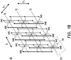
- Figures 1A , 1B , and 1C illustrate examples of a memory array 50, according to some embodiments.
- Figure 1A illustrates an example of a portion of the memory array 50 in a three-dimensional view
- Figure 1B illustrates a circuit diagram of the memory array 50
- Figure 1C illustrates a top down view of a portion of the memory array 50.
- the memory array 50 includes a plurality of memory cells 52, which may be arranged in a grid of rows and columns.
- the memory cells 52 may further stacked vertically to provide a three dimensional memory array, thereby increasing device density.
- the memory array 50 may be disposed in the back end of line (BEOL) of a semiconductor die.
- the memory array 50 may be disposed in the interconnect layers of the semiconductor die, such as, above one or more active devices (e.g., transistors) formed on a semiconductor substrate.
- BEOL back end of line
- the memory array 50 is a memory array such as a NOR memory array, or the like.
- Each memory cell 52 may include a transistor 54(such as a TFT) with an insulating, memory film 84 as a gate dielectric.
- a gate of each transistor 54 is electrically coupled to a respective word line (e.g., conductive line 72), a first source/drain region of each transistor 54 is electrically coupled to a respective bit line (e.g., conductive line 64B), and a second source/drain region of each transistor 54 is electrically coupled to a respective source line (e.g., conductive line 64S), which electrically couples the second source/drain region to ground.
- the memory cells 52 in a same horizontal row of the memory array 50 may share a common word line while the memory cells 52 in a same vertical column of the memory array 50 may share a common source line and a common bit line.
- the memory array 50 includes a plurality of vertically stacked conductive lines 72 (e.g., word lines) with dielectric layers 62 disposed between adjacent ones of the conductive lines 72.
- the conductive lines 72 extend in a direction D1 parallel to a major surface of an underlying substrate (not explicitly illustrated in Figures 1A and 1B ).
- the conductive lines 72 may be part of a staircase structure such that lower conductive lines 72 are longer than and extend laterally past endpoints of upper conductive lines 72.
- FIG 1A multiple, stacked layers of conductive lines 72 are illustrated with topmost conductive lines 72 being the shortest and bottommost conductive lines 72 being the longest. Respective lengths of the conductive lines 72 may increase in a direction towards the underlying substrate.
- each of the conductive lines 72 may be accessible from above the memory array 50, and conductive contacts 66 (see Figure 1C ) may be made to an exposed portion of each of the conductive lines 72.
- the conductive contacts 66 may be, e.g., vias that connect the exposed portions of the conductive lines 72 to interconnects 68(see Figure 1C ) of overlying interconnect layers, in embodiments where the memory array 50 is disposed in the interconnect layers of a semiconductor die.
- the memory array 50 further includes a plurality of conductive lines 64B (e.g., bit lines) and conductive lines 64S (e.g., source lines).
- the conductive lines 64B, 64S may each extend in a direction D 3 perpendicular to the conductive lines 72.
- Isolation regions 74 are disposed between and isolate adjacent ones of the conductive lines 64B and the conductive lines 64S. Pairs of the conductive lines 64B, 64S along with an intersecting conductive line 72 define boundaries of each memory cell 52, and anisolation region 76 is disposed between and isolates adjacent pairs of the conductive lines 64B, 64S.
- the conductive lines 64S are electrically coupled to ground.
- Figure 1A illustrates a particular placement of the conductive lines 64B relative the conductive lines 64S, it should be appreciated that the placement of the conductive lines 64B, 64S may be flipped in other embodiments.
- the memory array 50 may also include semiconductor layers 82.
- the semiconductor layers 82 may provide channel regions for the transistors 54 of the memory cells 52. For example, when an appropriate voltage (e.g., higher than a respective threshold voltage (V th ) of a corresponding transistor 54) is applied through a corresponding conductive line 72, a region of a semiconductor layer 82 that intersects the conductive line 72 may allow current to flow from the conductive lines 64B to the conductive lines 64S (e.g., in the direction indicated by arrow 56).
- V th threshold voltage
- a memory film 84 is disposed between the conductive lines 72 and the semiconductor layers 82, and the memory film 84 may provide gate dielectrics for the transistors 54.
- the memory film 84 comprises a ferroelectric material, such as a hafnium oxide, hafnium zirconium oxide, silicon-doped hafnium oxide, or the like.
- the memory array 50 may also be referred to as a ferroelectric random access memory (FERAM) array.
- FERAM ferroelectric random access memory
- the memory film 84 may be a multilayer structure comprising a layer of silicon nitride between two silicon oxide layers (e.g., an oxide-nitride-oxide (ONO) structure), a different ferroelectric material, a different type of memory layer (e.g., capable of storing a bit), or the like.
- silicon oxide layers e.g., an oxide-nitride-oxide (ONO) structure
- OEO oxide-nitride-oxide
- ferroelectric material e.g., capable of storing a bit
- the memory film 84 may be polarized in one of two different directions, and the polarization direction may be changed by applying an appropriate voltage differential across the memory film 84 and generating an appropriate electric field.
- the polarization may be relatively localized (e.g., generally contained within each boundaries of the memory cells 52), and a continuous region of the memory film 84 may extend across a plurality of memory cells 52.
- a threshold voltage of a corresponding transistor54 varies, and a digital value (e.g., 0 or 1) can be stored.
- a digital value e.g., 0 or 1
- the corresponding transistor54 may have a relatively low threshold voltage
- the corresponding transistor54 may have a relatively high threshold voltage.
- the difference between the two threshold voltages may be referred to as the threshold voltage shift.A larger threshold voltage shift makes it easier (e.g., less error prone) to read the digital value stored in the corresponding memory cell 52.
- a write voltage is applied across a portion of the memory film 84 corresponding to the memory cell 52.
- the write voltage can be applied, for example, by applying appropriate voltages to a corresponding conductive line 72 (e.g., the word line) and the corresponding conductive lines 64B, 64S (e.g., the bit line/source line).
- a polarization direction of the region of the memory film 84 can be changed.
- the corresponding threshold voltage of the corresponding transistor54 can also be switched from a low threshold voltage to a high threshold voltage or vice versa, and a digital value can be stored in the memory cell 52. Because the conductive lines 72 intersect the conductive lines 64B, 64S, individual memory cells 52 may be selected for the write operation.
- a read voltage (a voltage between the low and high threshold voltages) is applied to the corresponding conductive line 72 (e.g., the world line).
- the transistor54 of the memory cell 52 may or may not be turned on.
- the conductive line 64B may or may not be discharged through the conductive line 64S (e.g., a source line that is coupled to ground), and the digital value stored in the memory cell 52 can be determined. Because the conductive lines 72 intersect the conductive lines 64B, 64S, individual memory cells 52 may be selected for the read operation.
- Figure 1A further illustrates reference cross-sections of the memory array 50 that are used in later figures.
- Cross-section B-B' is along a longitudinal axis of conductive lines 72 and in a direction D 1 , for example, parallel to the direction of current flow of the transistors 54.
- Cross-section C-C' is perpendicular to cross-section B-B' and in a direction D 2 , for example, perpendicular to a longitudinal axis of the conductive lines 72. Subsequent figures refer to these reference cross-sections for clarity.
- FIGS 2 through 19C are views of intermediate stages in the manufacturing of a memory array 50, in accordance with some embodiments.
- Each memory cell 52of the memory array 50 includes a transistor 54 (see Figures 19B and 19C ).
- Figures 2 , 3 , 4 , 5 , 6 , 7 , 8 , 9 , 10 , 11 , 12 , 13 , 14 , 15 , 16 , 17 , 18 , and 19A are three-dimensional views.
- Figure 19B is a cross-sectional view shown along reference cross-section B-B' in Figure 1A .
- Figure 19C is a cross-sectional view shown along reference cross-section C-C in Figure 1A .
- a portion of the memory array 50 is illustrated. Some features, such as the staircase arrangement of the word lines (see Figure 1A ), are not shown in some figures for clarity of illustration.
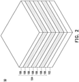
- a substrate 102 is provided.
- the substrate 102 may be a semiconductor substrate, such as a bulk semiconductor, a semiconductor-on-insulator (SOI) substrate, or the like, which may be doped (e.g., with a p-type or an n-type dopant) or undoped.
- the substrate 102 may be a wafer, such as a silicon wafer.
- SOI substrate is a layer of a semiconductor material formed on an insulator layer.
- the insulator layer may be, for example, a buried oxide (BOX) layer, a silicon oxide layer, or the like.
- the insulator layer is provided on a substrate, typically a silicon or glass substrate.
- the semiconductor material of the substrate 102 may include silicon; germanium; a compound semiconductor including silicon carbide, gallium arsenide, gallium phosphide, indium phosphide, indium arsenide, and/or indium antimonide; an alloy semiconductor including silicon germanium, gallium arsenide phosphide, aluminum indium arsenide, aluminum gallium arsenide, gallium indium arsenide, gallium indium phosphide, and/or gallium indium arsenide phosphide; or combinations thereof.
- the substrate 102 may include a dielectric material.
- the substrate 102 may be a dielectric layer, or may include a dielectric layer on a semiconductor substrate.
- Acceptable dielectric materials for the substrate 102 include oxides such as silicon oxide or aluminum oxide; nitrides such as silicon nitride; carbides such as silicon carbide; the like; or combinations thereof such as silicon oxynitride, silicon oxycarbide, silicon carbonitride, silicon oxycarbonitride or the like.
- the substrate 102 is formed of silicon carbide.
- a multilayer stack 104 is formed over the substrate 102.
- the multilayer stack 104 includes alternating dielectric layers 106 and sacrificial layers 108.
- the dielectric layers 106 are formed of a first dielectric material
- the sacrificial layers 108 are formed of a second dielectric material.
- the dielectric materials may each be selected from the candidate dielectric materials of the substrate 102.
- the multilayer stack 104 will be patterned in subsequent processing. As such, the dielectric materials of the dielectric layers 106 and the sacrificial layers 108 both have a high etching selectivity from the etching of the material of the substrate 102.
- the patterned dielectric layers 106 will be used to isolate subsequently formed transistors.
- the patterned sacrificial layers 108 may also be referred to as dummy layers, and will be selectively replaced with word lines for the transistors in subsequent processing.
- the second dielectric material of the sacrificial layers 108 also has a high etching selectivity from the etching of the first dielectric material of the dielectric layers 106.
- the dielectric layers 106 can be formed of silicon oxide, and the sacrificial layers 108 can be formed of silicon nitride. Other combinations of dielectric materials having acceptable etching selectivity from one another may also be used.
- Each layer of the multilayer stack 104 may be formed by an acceptable deposition process such as chemical vapor deposition (CVD), atomic layer deposition (ALD), or the like.
- a thickness of each of the layers may be in the range of about 40 nm to about 50 nm.
- the dielectric layers 106 are formed to a different thickness than the sacrificial layers 108.
- the sacrificial layers 108 can be formed to a greater thickness than the dielectric layers 106.
- the multilayer stack 104 includes five of the dielectric layers 106 and four of the sacrificial layers 108. It should be appreciated that the multilayer stack 104 may include other quantities of the dielectric layers 106 and the sacrificial layers 108.
- the multilayer stack 104 can have an overall height H 1 in the range of about 1000 nm to about 10000 nm.
- Figures 3 through 10 illustrate a process in which a multiple-patterning process is used to form some of the features of the transistors.
- the multiple-patterning process may be a double patterning process, a quadruple patterning process, or the like.
- Figures 3 through 10 illustrate a double patterning process.
- trenches 110A are patterned in portions of the multilayer stack 104 with a first etching process, and features for a first subset of the transistors are formed in the trenches 110A.
- Trenches 110B are then patterned in other portions of the multilayer stack 104 with a second etching process, and features for a second subset of the transistors are formed in the trenches 110B.
- Forming the features of the transistors with a multiple-patterning process allowseach patterning process to be performed with a low pattern density, which can help reduce defects while still allowing the memory array 50 to have sufficient memory cell density .Further, forming the features of the transistors with a multiple-patterning process also allows each patterned portion of the multilayer stack 104 to avoid having an excessively large aspect ratio, thereby improving the structural stability of the resulting memory array.
- a single patterning process may also be used to form some of the features of the transistors.
- trenches 110A are patterned in the multilayer stack 104.
- the trenches 110A extend through the multilayer stack 104 and expose the substrate 102.
- the trenches 110A extend through some but not all layers of the multilayer stack 104.
- the trenches 110A may be patterned using acceptable photolithography and etching techniques, such as with an etching process that is selective to the multilayer stack 104 (e.g., selectively removes the dielectric materials of the dielectric layers 106 and the sacrificial layers 108 at a faster rate than the material of the substrate 102).
- the etching may be any acceptable etch process, such as a reactive ion etch (RIE), neutral beam etch (NBE), the like, or a combination thereof.
- the etching may be anisotropic.
- the substrate 102 is formed of silicon carbide
- the dielectric layers 106 are formed of silicon oxide
- the sacrificial layers 108 are formed of silicon nitride
- the trenches 110A can be formed by a dry etch using a fluorine-based gas (e.g., C 4 F 6 ) mixed with hydrogen (H 2 ) or oxygen (O2) gas.
- a fluorine-based gas e.g., C 4 F 6
- H 2 hydrogen
- O2 oxygen
- Each portion of the multilayer stack 104 has a width W 1 in the second direction D 2 (see Figures 1A and 1B ), which can be in the range of about 50 nm to about 500 nm. Further, each portion of the multilayer stack 104 is separated by a separation distance S 1 in the second direction D 2 , which can be in the range of about 50 nm to about 200 nm.
- the trenches 110A are expanded to form sidewall recesses 112A. Specifically, portions of the sidewalls of the sacrificial layers 108 exposed by the trenches 110A are recessed from the portions of the sidewalls of the dielectric layers 106 exposed by the trenches 110A to form the sidewall recesses 112A. Although sidewalls of the sacrificial layers 108 are illustrated as being straight, the sidewalls may be concave or convex.
- the sidewall recesses 112A may be formed by an acceptable etching process, such as one that is selective to the material of the sacrificial layers 108 (e.g., selectively removes the material of the sacrificial layers 108 at a faster rate than the material(s) of the dielectric layers 106 and the substrate 102).
- the etching may be isotropic.
- the substrate 102 is formed of silicon carbide
- the dielectric layers 106 are formed of silicon oxide
- the trenches 110A can be expanded by a wet etch using phosphoric acid (H 3 PO 4 ).
- a dry etch selective to the material of the sacrificial layers 108 may be used.
- the sidewall recesses 112A After formation, the sidewall recesses 112A have a depth D 4 in the second direction D 2 (see Figures 1A and 1B ), extending past the sidewalls of the dielectric layers 106. Timed etch processes may be used to stop the etching of the sidewall recesses 112A after the sidewall recesses 112A reach a desired depth D 4 .
- the sidewall recesses 112A can have a depth D 4 in the range of about 10 nm to about 60 nm.Forming the sidewall recesses 112A can reduce the widths of the sacrificial layers 108 by about 5% to about 25%.
- the sacrificial layers 108 can have a width W 2 in the second direction D 2 , which can be in the range of about 50 nm to about 450 nm.
- conductive features 114A are formed in the sidewall recesses 112A, thus completing a process for replacing first portions of the sacrificial layers 108.
- the conductive features 114A may each include one or more layers, such as seed layers, glue layers, barrier layers, diffusion layers, fill layers, and the like.
- the conductive features 114A each include a seed layer 114A S (or barrier layer) and a main layer 114A M .
- Each seed layer 114A S extends along three sides (e.g., the top surface, a sidewall, and the bottom surface) of a corresponding main layer 114A M located within a correspondingsidewall recesses 112A.
- the seed layers 114A S are formed of a first conductive materialthat can be utilized to help grow or to help adhere a subsequently deposited material, such as a metal nitride, such as titanium nitride, tantalum nitride, molybdenumnitride, zirconium nitride, hafnium nitride, or the like.
- the mainlayers 114A M may are formed of a second conductive material, such as a metal, such as tungsten, ruthenium, molybdenum,cobalt, aluminum, nickel,copper, silver, gold, alloys thereof, or the like.
- the material of the seed layers 114A S is one that has good adhesion to the material of the dielectric layers 106
- the material of the mainlayers 114A M is one that has good adhesion to the material of the seed layers 114A S .
- the dielectric layers 106 are formed of an oxide such as silicon oxide
- the seed layers 114A S can be formed of titanium nitride ortantalum nitride
- the mainlayers 114A M can be formed of tungsten.
- Thematerials of the seed layers 114A S and mainlayers 114A M may be formed by acceptable deposition processes such as chemical vapor deposition (CVD), atomic layer deposition (ALD), or the like.
- acceptable deposition processes such as chemical vapor deposition (CVD), atomic layer deposition (ALD), or the like.
- An acceptable etch process such as a dry etch (e.g., a reactive ion etch (RIE), neutral beam etch (NBE), the like), a wet etch, the like, or a combination thereof, may be performed to remove excess material from the sidewalls of the dielectric layers 106 and the top surface of the substrate 102.
- the etching may be anisotropic.
- Each of the conductive features 114A can have a similar overall thickness as the sacrificial layers 108 (discussed above for Figure 2 ), and can have a similar overall width as the depth D 4 of the sidewall recesses 112A (discussed above for Figure 4 ).Each seed layer 114A S can have a thickness in the range of about 1 nm to about 10 nm, and each main layer 114A M can have a thickness in the range of about 15 nm to about 35 nm, with the thickness of theseed layer 114A S being greater than the thickness of themain layer 114A M .
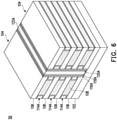
- memory films 116A, semiconductor layers 118A, back gate isolators 120A, and isolation regions 122A are formed in the trenches 110A.
- the semiconductor layers 118A and the back gate isolators 120A are formed over thememory films 116A.
- Theisolation regions 122A extend through the semiconductor layers 118A, thus separating the semiconductor layers 118A of horizontally adjacent transistors along the direction D 2 (see Figures 1A and 1B ).
- the isolation regions 122A are formed over the memory films 116A.
- the isolation regions 122A also extend through thememory films 116A and the substrate 102,thus separating the memory films 116A of horizontally adjacent transistors along the direction D 2 .
- Portions of the memory films 116A providedata storage layers for the transistors and portions of the semiconductor layers 118Aprovide channel regions for the transistors.
- theback gate isolators 120A will be patterned and used to help form T-shaped source/drain regionsof the transistors.
- the T-shaped source/drain regions have main regions and extension regions.
- Theback gate isolators 120A will be patterned so that themain source/drain regions may contact the semiconductor layers 118A, but thesource/drainextension regions are separated from the portions of the semiconductor layers 118A thatprovidethe channel regions, thus preventing shorting of the channel regions.
- Thesource/drainextension regions can act as back gates to help control (e.g., reduce) the surface potential of the semiconductor layers 118 (particularly the portions of the semiconductor layers 118 distal the word lines 114) duringwrite operations.
- the window for write operations may thus be widened.
- the memory films 116A are formed of an acceptable material for storing digital values.
- the memory films 116A are formed of a high-k ferroelectric material, such ashafnium zirconium oxide (HfZrO); zirconium oxide (ZrO); hafnium oxide (HfO) doped with lanthanum (La), silicon (Si), aluminum (Al), or the like; undoped hafnium oxide (HfO); or the like.
- the memory films 116A include one or more low-k dielectric materials, such as silicon nitride, silicon oxide, silicon oxynitride, or the like.
- the material of thememory films 116A may be formed by an acceptable deposition process such as ALD, CVD, physical vapor deposition (PVD), or the like.
- the memory films 116A are HfZrO deposited by ALD.
- the semiconductor layers 118A formed of an acceptable material for providing channel regions for the transistors, such as indium gallium zinc oxide (IGZO), indium tin oxide (ITO), indium gallium zinc tin oxide (IGZTO), zinc oxide (ZnO), polysilicon, amorphous silicon, or the like.
- the material of the semiconductor layers 118A may be formed by an acceptable deposition process such as ALD, CVD, PVD, or the like.In some embodiments, the semiconductor layers 118Aare formed of IGZTO deposited by ALD.
- the back gate isolators 120A are formed of an acceptable material for electrically insulating subsequently formed source/drainextension regions from the portions of the semiconductor layers 118A thatprovide channel regions. In some embodiments, theback gate isolators 120A are formed of a dielectric material.
- Acceptable dielectric materials for the back gate isolators 120A include oxides such as silicon oxide or aluminum oxide; nitrides such as silicon nitride; carbides such as silicon carbide; the like; or combinations thereof such as silicon oxynitride, silicon oxycarbide, silicon carbonitride, silicon oxycarbonitride or the like.
- the material of theback gate isolators 120A may be formed by an acceptable deposition process such as ALD, CVD, flowable CVD (FCVD), or the like.
- the back gate isolators 120A are formed of an oxide such as aluminum oxide deposited by ALD.
- the isolation regions 122A are formed of an acceptablematerial for protecting and electrically isolating the underlyingmemory films 116A.
- Acceptable dielectric materials for theisolation regions 122A include oxides such as silicon oxide or aluminum oxide; nitrides such as silicon nitride; carbides such as silicon carbide; the like; or combinations thereof such as silicon oxynitride, silicon oxycarbide, silicon carbonitride, silicon oxycarbonitride or the like.
- the material of theisolation regions 122 may be formed by an acceptable deposition process such as ALD, CVD, flowable CVD (FCVD), or the like.
- the isolation regions 122A and theback gate isolators 120A are formed of different dielectric materials so that the material of theisolation regions 122A has a high etching selectivity from the etching of the material of theback gate isolators 120A.
- the isolation regions 122A are formed of an oxide such as silicon oxide deposited by FCVD.
- the memory films 116A, the semiconductor layers 118A, the back gate isolators 120A, and the isolation regions 122A may be formed by a combination of deposition, etching, and planarization.
- a tunneling layer can be conformally deposited on themultilayer stack 104 and in the trenches 110A (e.g., on the sidewalls of the conductive features 114A and the sidewalls of the dielectric layers 106).
- a semiconductor layer can then be conformally deposited on the tunneling layer.
- a dielectric layer can then be conformally deposited on the semiconductor layer.
- the dielectric layer can then be patterned bya suitable etching process, such as an anisotropicetch using the tunneling layer as an etch stop layer.
- Thesemiconductor layer can then be patterned by a suitable etching process, such as an anisotropicetchusing thepatterneddielectric layer as an etching mask.
- Anisolation material can then be conformally deposited in the remaining portions of trenches 110A (e.g., on the patterned semiconductor layer, the patterneddielectric layer, and the exposed portions of the tunneling layer).
- a removal process is then applied to the various layers to remove excess materials over the topmost dielectric layers 106/sacrificial layers 108.
- the removal process may be a planarization process such as a chemical mechanical polish (CMP), an etch-back, combinations thereof, or the like.
- CMP chemical mechanical polish
- the portions of the tunneling layer, the semiconductor layer, the dielectric layer, and theisolation material remaining in the trenches 110A forms the memory films 116A, the semiconductor layers 118A, the back gate isolators 120A, and the isolation regions 122A,respectively.
- the planarization process exposes the topmost dielectric layers 106/sacrificial layers 108 such that top surfaces of the memory films 116A, the semiconductor layers 118A, the back gate isolators 120A, the isolation regions 122A, and the topmost dielectric layers 106/sacrificial layers 108 are coplanar (within process variations) after the planarization process.
- the isolation regions 122A can be formed to also extend through the through thememory films 116A and the substrate 102.
- the memory array 50 is embedded in another semiconductor device.
- the memory array 50 can be formed in the interconnect structure of a semiconductor device.
- openings can be formed through thememory films 116A and the substrate 102before depositing the isolation material of theisolation regions 122A.
- Portions of theisolation regions 122A will be subsequently replaced withsource/drain regions of the transistors so that the source/drain regions are connected to metallization layers of the interconnect structure that underly underlying thememory array 50.
- a suitable etching process can be performed on the memory films 116A and the substrate 102 using the semiconductor layers 118A and the back gate isolators 120A as an etching mask.
- the etching process is selective to the memory films 116A and the substrate 102 (e.g., selectively removes the material(s) of the memory films 116A and the substrate 102 at a faster rate than the material(s)the semiconductor layers 118A and the back gate isolators 120A).
- the etch may be anisotropic.
- theetching process includes multiple etches. For example, a first etch can be performed to extend the openings through the memory films 116A, and a second etch can be performed to extend the openings through the substrate 102. After the openings are formed, the isolation regions 122A can be formed by a similar manner as described above.
- trenches 110B are patterned in the multilayer stack 104.
- the trenches 110B extend through the multilayer stack 104 and expose the substrate 102.
- the trenches 110B extend through some but not all layers of the multilayer stack 104.
- the trenches 110B may be patterned using acceptable photolithography and etching techniques, such as with an etching process that is selective to the multilayer stack 104 (e.g., selectively removes the dielectric materials of the dielectric layers 106 and the sacrificial layers 108 at a faster rate than the material of the substrate 102).
- the etching may be any acceptable etch process, and in some embodiments, may be similar to the etch used to form the trenches 110A (discussed above for Figure 3 ).
- respective portions of the multilayer stack 104 are disposed between respective pairs of the trenches 110A, 110B.
- Each portion of the multilayer stack 104 has a width W 3 in the second direction D 2 (see Figures 1A and 1B ), which can be in the range of about 50 nm to about 500 nm.
- each portion of the multilayer stack 104 is separated by a separation distance S 2 in the second direction D 2 , which can be in the range of about 50 nm to about 200 nm.Misalignment may occur when patterning thetrenches 110B.
- the patterned portions of the multilayer stack 104 do not all have a samewidth W 3 .
- the patterned portions of the multilayer stack 104 have a samewidth W 3 .
- the trenches 110B are expanded to form sidewall recesses 112B. Specifically, the remaining portions of the sacrificial layers 108 are removed to form the sidewall recesses 112B.
- Thesidewall recesses 112B thus expose the sidewalls of the conductive features 114A(e.g., the sidewalls of theseed layers 114A S ).
- the sidewall recesses 112B may be formed by an acceptable etching process, such as one that is selective to the material of the sacrificial layers 108 (e.g., selectively removes the material of the sacrificial layers 108 at a faster rate than the material(s) of the dielectric layers 106 and the substrate 102).
- the etching may be any acceptable etch process, and in some embodiments, may be similar to the etch used to form the sidewall recesses 112A (discussed above for Figure 4 ).
- the sidewall recesses 112B After formation, the sidewall recesses 112B have a depth D 5 in the second direction D 2 (see Figures 1A and 1B ), extending past the sidewalls of the dielectric layers 106. Timed etch processes may be used to stop the etching of the sidewall recesses 112B after the sidewall recesses 112B reach a desired depth D 5 . As noted above,misalignment may occur when patterning thetrenches 110B. When misalignment occurs, the depth D 5 is different from (e.g., greater than or less than) the depth D 4 (discussed above for Figure 4 ). When no misalignment occurs, the depth D 5 is similar to the depth D 4 .
- conductive features 114B are formed in the sidewall recesses 112B, thus completing a process for replacing second portions of the sacrificial layers 108.
- the conductive features 114B may be formed of materials that are selected from the same group of candidate materials of the conductive features 114A, which may be formed using methods that are selected from the same group of candidate methods for forming the materialsof the conductive features 114A.
- the conductive features 114A and the conductive features 114B may be formed from the same material, or may include different materials.
- theconductive features 114B each include a seed layer 114B S (or barrier layer) and a main layer 114B M .
- the seed layers 114B S and the main layers 114B M can have similar thicknesses as the seed layers 114A S and the main layers 114A M , respectively.
- the seed layers 114A S and theseed layers 114B S are formed of similar materials, in which case the seed layers 114A S and theseed layers 114B S may merge during formation such that no discernable interfaces exist between them.
- the seed layers 114A S and theseed layers 114B S are formed of different materials, in which case the seed layers 114A S and theseed layers 114B S may not merge during formation such that discernable interfaces exist between them.As noted above,misalignment may occur when patterning thetrenches 110B.
- each seed layer 114A S , 114B S are laterally disposed between a main layer 114A M and a main layer 114B M .
- the conductive features 114A and theconductive features 114B are collectively referred to as word lines 114 of the memory array 50. Adjacent pairs of the conductive features 114A and theconductive features 114B are in physical contact with one another and are electrically coupled to one another. Thus, each pair of conductive features 114A, 114B functions as a single word line 114.
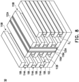
- the memory films 116B, semiconductor layers 118B, back gate isolators 120B, and isolation regions 122B are formed in the trenches 110B.
- the semiconductor layers 118B and the back gate isolators 120B are formed over thememory films 116B.
- Theisolation regions 122B extend through the semiconductor layers 118B, thus separating the semiconductor layers 118B of horizontally adjacent transistors along the direction D 2 (see Figures 1A and 1B ).
- the isolation regions 122B are formed over the memory films 116B.
- the isolation regions 122B also extend through thememory films 116Band the substrate 102,thus separating the memory films 116B of horizontally adjacent transistors along the direction D 2 .
- the memory films 116B may be formed of a material that is selected from the same group of candidate materials of the memory films 116A, which may be formed using a method that is selected from the same group of candidate methods for forming the material of the memory films 116A.
- the memory films 116A and the memory films 116B may be formed from the same material, or may include different materials.
- Thememory films 116A and the memory films 116B are collectively referred to as memory films 116.A thickness of the memory films 116can be in the range of about 2 nm to about 20 nm.
- the semiconductor layers 118B may be formed of a material that is selected from the same group of candidate materials of the semiconductor layers 118A, which may be formed using a method that is selected from the same group of candidate methods for forming the material of the semiconductor layers 118A.
- the semiconductor layers 118A and the semiconductor layers 118B may be formed from the same material, or may include different materials. Thesemiconductor layers 118A and the semiconductor layers 118B are collectively referred to as semiconductor layers 118.A thickness of the semiconductor layers 118can be in the range of about 9 nm to about 11 nm.
- the back gate isolators 120B may be formed of a material that is selected from the same group of candidate materials of the back gate isolators 120A, which may be formed using a method that is selected from the same group of candidate methods for forming the material of the back gate isolators 120A.
- the back gate isolators 120A and the back gate isolators 120B may be formed from the same material, or may include different materials.
- Theback gate isolators 120A and the back gate isolators 120B are collectively referred to as back gate isolators 120.
- a thickness of the back gate isolators 120 can be in the range of about 1 nm to about 20 nm.
- the isolation regions 122B may be formed of a material that is selected from the same group of candidate materials of the isolation regions 122A, which may be formed using a method that is selected from the same group of candidate methods for forming the material of the isolation regions 122A.
- the isolation regions 122A and the isolation regions 122B may be formed from the same material, or may include different materials.
- the isolation regions 122B and theback gate isolators 120B are formed of different dielectric materials so that the material of theisolation regions 122B has a high etching selectivity from the etching of the material of theback gate isolators 120B.
- Theisolation regions 122A and the isolation regions 122B are collectively referred to as isolation regions 122.
- a thickness of the isolation regions 122 can be in the range of about 42 nm to about 192 nm.
- the memory films 116B, the semiconductor layers 118B, the back gate isolators 120B, and the isolation regions 122B may be formed by a combination of deposition, etching, and planarization.
- the memory films 116B, the semiconductor layers 118B, the back gate isolators 120B, and the isolation regions 122B may be formed by similar steps (discussed above for Figure 6 ) as those used to form the memory films 116A, the semiconductor layers 118A, the back gate isolators 120A, and the isolation regions 122A.
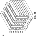
- Figures 11 through 18 illustrate a process in which portions of the isolation regions 122 are replaced with the remaining features of the transistors. Specifically, portions of the isolation regions 122 are replaced with isolation regions 142 (see Figure 16 ), and with bit lines 146B and source lines 146S (see Figure 18 ). The remaining portions of the isolation regions 122 separate the features of horizontally adjacent transistorsalong the direction D 1 (see Figures 1A and 1B ). The bit lines 146B and the source lines 146S also act as source/drain regions of the transistors.
- the back gate isolators 120 are patterned. The patternedback gate isolators 120 allow portions of the bit lines 146B/source lines 146S to also act as back gates duringwrite operations.
- the openings 130 may be formed with an etching process that is selective to the isolation regions 122 (e.g., selectively removes the material of the isolation regions 122 at a faster rate than the materials of the memory films 116 and the back gate isolators 120).
- the etching may be any acceptable etch process, such as a reactive ion etch (RIE), neutral beam etch (NBE), the like, or a combination thereof.
- RIE reactive ion etch
- NBE neutral beam etch
- the etching may be anisotropic.
- the openings 130 can be formed through the isolation regions 122 by a dry etch using ammonia (NH3) and hydrogen fluoride (HF) gas, performed with an etching mask having a pattern of the openings 130.
- NH3 ammonia
- HF hydrogen fluoride
- sacrificial regions 132 are formed in the openings 130.
- Thesacrificial regions 132 are formed of a sacrificial material, such as a dielectric material, which will be replaced with bit lines and source lines in subsequent processing.
- the dielectric material of the sacrificial regions 132 has a high etching selectivity from the etching of the materials of the memory films 116, the semiconductor layers 118, and the back gate isolators 120.
- Acceptable dielectric materials for the sacrificial regions 132 include oxides such as silicon oxide or aluminum oxide; nitrides such as silicon nitride; carbides such as silicon carbide; the like; or combinations thereof such as silicon oxynitride, silicon oxycarbide, silicon carbonitride, silicon oxycarbonitride or the like.
- the material of the sacrificial regions 132 may be formed by an acceptable deposition process such as ALD, CVD, flowable CVD (FCVD), or the like.
- the sacrificial regions 132 are formed of a nitride such as silicon nitride deposited by CVD.
- a removal process may be applied to the material of the sacrificial regions 132 to remove excess of the material over the topmost dielectric layers 106/sacrificial layers 108.
- the removal process may be a planarization process such as a chemical mechanical polish (CMP), an etch-back, combinations thereof, or the like.
- CMP chemical mechanical polish
- the planarization process exposes the topmost dielectric layers 106/sacrificial layers 108 such that top surfaces of the sacrificial regions 132and the topmost dielectric layers 106/sacrificial layers 108 are coplanar (within process variations) after the planarization process.
- the back gate isolators 120 and the sacrificial regions 132 are patterned to form openings 136.
- the openings 136 may be formed with an etching process that is selective to the back gate isolators 120 and the sacrificial regions 132 (e.g., selectively removes the materials of the back gate isolators 120 and the sacrificial regions 132 at a faster rate than the materials of the semiconductor layers 118 and/or the memory films 116).
- the etching may be any acceptable etch process, such as a reactive ion etch (RIE), neutral beam etch (NBE), the like, or a combination thereof.
- the etching may be anisotropic.
- the openings 136 can be formed through the back gate isolators 120 and the sacrificial regions 132 bya dry etch using a fluorine-based gas (e.g., C 4 F 6 ) mixed with hydrogen (H 2 ) or oxygen (O2) gas, performed with an etching mask having a pattern of the openings 136.
- a fluorine-based gas e.g., C 4 F 6
- each sacrificial region 132 thus has first portions 132A and a second portion 132B.
- thesacrificial regions 132 will be replaced with bit lines and source lines in subsequent processing, and the bit lines/source lines will have main regions and extension regions.
- the first portions 132A of the sacrificial region 132 correspond to the portions of the sacrificial material that were not removed when forming the openings 136, and will be replaced with the extension regions of thebit lines/source lines.
- the second portions 132B of the sacrificial region 132 correspond to the portions of the sacrificial material that were redeposited in the openings 136, and will be replaced with the main regionsof thebit lines/source lines.
- the portions 132A, 132B of the sacrificial regions 132 may merge during redeposition such that no discernable interfaces exist between them.
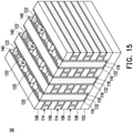
- openings 140 for isolation regions are formed through the sacrificial regions 132.
- the openings 140 divide the sacrificial regions 132 into portions that will be replaced with bit lines and source linesin subsequent processing.
- the openings 140 may be formed with an etching process that is selective to the sacrificial regions 132 (e.g., selectively removes the material of the sacrificial regions 132 at a faster rate than the material of the memory films 116).
- the etching may be any acceptable etch process, such as a reactive ion etch (RIE), neutral beam etch (NBE), the like, or a combination thereof.
- the etching may be anisotropic.
- the openings 140 can be formed through the sacrificial regions 132 by a dry etch using a fluorine-based gas (e.g., C 4 F 6 ) mixed with hydrogen (H 2 ) or oxygen (O2) gas, performed with an etching mask having a pattern of the openings 140.
- a fluorine-based gas e.g., C 4 F 6
- hydrogen (H 2 ) or oxygen (O2) gas e.g., hydrogen (H 2 ) or oxygen (O2) gas
- the semiconductor layers 118 are patterned during processing so that the semiconductor layers 118 of horizontally adjacent transistors are separated along the direction D1 (see Figures 1A and 1B ). As will be discussed in greater detail below, the semiconductor layers 118 can be patterned at one of several steps during processing, depending on the desired widths of the divided semiconductor layers 118. In this embodiment, the semiconductor layers 118 are concurrently patterned with the patterning of the sacrificial regions 132/openings 140 (see Figure 15 ). In another embodiment, the semiconductor layers 118are concurrently patterned with the patterning of the back gate isolators 120/openings 136 (see Figure 13).
- the semiconductor layers 118 are patterned in a separate step after the patterning of the back gate isolators 120/openings 136 (see Figure 13) but before there deposition of the material of the sacrificial regions 132 in the openings 136 (see Figure 14 ) or the patterning of the sacrificial regions 132/openings 140 (see Figure 15 ).
- the semiconductor layers 118 may be patterned with an etching process that is selective to the semiconductor layers 118(e.g., selectively removes the material of the semiconductor layers 118at a faster rate than the material of the memory films 116).
- the etching may be any acceptable etch process, such as a reactive ion etch (RIE), neutral beam etch (NBE), the like, or a combination thereof.
- RIE reactive ion etch
- NBE neutral beam etch
- the etching may be anisotropic.
- the semiconductor layers 118 may be patterned bya dry etch using Cl 2 , BCl 3 , CF 4 , SF 6 , or the like.
- isolation regions 142 are formed in the openings 140.
- the isolation regions 142 thus extend through the sacrificial regions 132.
- the isolation regions 142 may be formed of a material that is selected from the same group of candidate materials of the isolation regions 122, which may be formed using a method that is selected from the same group of candidate methods for forming the material of the isolation regions 122.
- the isolation regions 122 and the isolation regions 142 may be formed from the same material, or may include different materials.
- the isolation regions 142 are formed of silicon oxide deposited by CVD.
- an isolation material is formed in the openings 140.
- a removal process is then applied to the various layers to remove excess isolation material over the topmost dielectric layer 106/word line 114.
- the removal process may be a planarization process such as a chemical mechanical polish (CMP), an etch-back, combinations thereof, or the like.
- CMP chemical mechanical polish
- the remaining isolation material forms the isolation regions 142 in the openings 140.
- the sacrificial regions 132 are removed to form openings 144.
- the openings 144 may be formed with an etching process that is selective to the sacrificial regions 132 (e.g., selectively removes the material of the sacrificial regions 132 at a faster rate than the materials of the isolation regions 142, the back gate isolators 120,theisolation regions 122,the semiconductor layers 118,and the memory films 116).
- the etching may be isotropic.
- the openings 144 can be formed by a wet etch using phosphoric acid (H 3 PO4).
- a dry etch selective to the material of the sacrificial regions 132 may be used.
- bit lines 146B and source lines 146S are formed in the openings 144.
- the bit lines 146B and the source lines 146S are conductive pillars, and may also be referred to as bit line pillars and source line pillars.
- Each transistor will include a bit line 146B and a source line 146S, with anisolation region 122 disposed between thebit line 146B and the source line 146S.
- the bit lines 146B/source lines 146S extend though the semiconductor layers 118.
- the bit lines 146B/source lines 146S also extend through the memory films 116and the substrate 102.
- a liner such as a diffusion barrier layer, an adhesion layer, or the like, and a main layer are formed in the openings 144.
- the liner may be formed of a conductive material such as titanium, titanium nitride, tantalum, tantalum nitride, or the like, which may be deposited by a conformal deposition process, such as atomic layer deposition (ALD), chemical vapor deposition (CVD), physical vapor deposition (PVD), or the like.
- the liner may include an adhesion layer and at least a portion of the adhesion layer may be treated to form a diffusion barrier layer.
- the main layer may be formed of a conductive material such as tungsten, cobalt, ruthenium, aluminum, nickel, copper, a copper alloy, silver, gold, or the like, which may be deposited by ALD, CVD, PVD, or the like.
- the bit lines 146B/source lines 146S include a liner formed of titanium nitride and a main layer formed of tungsten.
- a removal process is then applied to the various layers to remove excess material(s) of the bit lines 146B/source lines 146S over the topmost dielectric layers 106/word lines 114.
- the removal process may be a planarization process such as a chemical mechanical polish (CMP), an etch-back, combinations thereof, or the like.
- CMP chemical mechanical polish
- the remaining material(s) in the openings 144 form the bit lines 146B/source lines 146S.
- the planarization process exposes the topmost dielectric layers 106/word lines 114 such that top surfaces of the bit lines 146B/source lines 146S, the isolation regions 142, the isolation regions 122, the back gate isolators 120, the semiconductor layers 118, the memory films 116, and the topmost dielectric layers 106/word lines 114 are coplanar (within process variations) after the planarization process.
- Thebit lines 146B/source lines 146S each have T-shaped cross-sections in the top-down view. Specifically, the bit lines 146B have main regions 146B M that extend along the sidewalls of the semiconductor layers 118, and have extension regions 146B E that extend along the sidewalls of theback gate isolators 120. Similarly, the source lines 146S have main regions 146S M that extend along the sidewalls of the semiconductor layers 118, and have extension regions 146S E that extend along the sidewalls of theback gate isolators 120.
- the extension regions 146B E , 146S E and the isolation regions 122 each have the same width in the second direction D 2 (see Figures 1A and 1B ).
- the patterned back gate isolators 120 allow themain regions 146B M ,146S M to contact the semiconductor layers 118, but keeps the extension regions 146B E , 146S E separated from the portions of the semiconductor layers 118 thatprovide channel regions. As such, the extension regions 146B E , 146S E can act as back gates without shorting the channel regions.
- an interconnect structure 160 is formed over the intermediate structure.
- the interconnect structure 160 may include, e.g., metallization patterns 162 in a dielectric material 164 (not shown in Figure 19A , see Figures 19B and 19C ).
- the dielectric material 164 may include one or more dielectric layers, such as one or more layers of a low-k (LK) or an extra low-K (ELK) dielectric material.
- the metallization patterns 162 may be metal interconnects (e.g., conductive lines 162L, conductive vias 162V, etc.) formed in the dielectric material 164.
- the interconnect structure 160 may be formed by a damascene process, such as a single damascene process, a dual damascene process, or the like.
- the metallization patterns 162 of the interconnect structure 160 are electrically connected to the bit lines 146B/source lines 146S, and interconnect the transistors 54 to form functional memories.
- the dielectric layers 106 and the word lines 114 may be formed in a staircase structure.
- the dielectric layers 106 and the word lines 114 may be patterned to form the staircase structure at any suitable step before the formation of the interconnect structure 160.
- Forming the interconnect structure 160 includes forming conductive contacts that are connected to the exposed portions of each of the word lines 114.
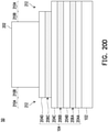
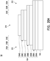
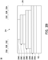
- Figures 20A through 20J are views of intermediate stages in the manufacturing of a staircase structure of a memory array 50, in accordance with some embodiments.
- Figures 20A through 20J are cross-sectional views illustrated along reference cross-section B-B' illustrated in Figure 1A .
- the multilayer stack 104 is patterned to form a staircase structure after the sacrificial layers 108 are replaced with the word lines 114. It should be appreciated that the process shown may be performed at other suitable steps of processing.
- a mask 202 is formed over the multilayer stack 104.
- the multilayer stack 104 comprises alternating dielectric layers 204 (such as the dielectric layers 106 discussed above, labeled 204A, 204B, 204C, 204D) and conductive layers 206 (such as the word lines 114 discussed above, labeled 206A, 206B, 206C).
- the mask 202 may be a photoresist or the like, which can be formed by a spin-on technique or the like.
- the mask 202 is patterned to expose the multilayer stack 104 in regions 210A while masking remaining portions of the multilayer stack 104.
- a topmost layer of the multilayer stack 104 e.g., the dielectric layer 204D
- the mask 202 may be patterned using acceptable photolithography techniques
- the exposed portions of the multilayer stack 104 in the regions 210A are etched using the mask 202 as an etching mask.
- the etching may be any acceptable etch process, such as by wet or dry etching, a reactive ion etch (RIE), neutral beam etch (NBE), the like, or a combination thereof.
- the etching may be anisotropic.
- the etching may remove portions of the dielectric layer 204D and conductive layer 206C in the regions 210A and define openings 212. Because the dielectric layer 204D and the conductive layer 206C have different material compositions, etchants used to remove exposed portions of these layers may be different.
- the conductive layer 206C acts as an etch stop layer while etching the dielectric layer 204D
- the dielectric layer 204C acts as an etch stop layer while etching conductive layer 206C.
- the portions of the conductive layer 206C and the dielectric layer 204D may be selectively removed without removing remaining layers of the multilayer stack 104, and the openings 212 may be extended to a desired depth.
- a timed etch processes may be used to stop the etching of the openings 212 after the openings 212 reach a desired depth.
- the dielectric layer 204C is exposed in the regions 210A.
- the mask 202 is trimmed to expose additional portions of the multilayer stack 104.
- the mask 202 can be trimmed using acceptable photolithography and/or etching techniques.
- a width of the mask 202 is reduced, and portions the multilayer stack 104 in regions 210B may also be exposed.
- a top surface of the dielectric layer 204C may be exposed in the regions 210A, and a top surface of the dielectric layer 204D may be exposed in the regions 210B.
- portions of the dielectric layer 204D, the conductive layer 206C, the dielectric layer 204C, and the conductive layer 206B in the regions 210A and 210B are removed by acceptable etching processes using the mask 202 as an etching mask.
- the etching may be any acceptable etch process, such as by wet or dry etching, a reactive ion etch (RIE), neutral beam etch (NBE), the like, or a combination thereof.
- the etching may be anisotropic.
- the etching may extend the openings 212 further into the multilayer stack 104.
- the conductive layer 206C acts as an etch stop layer while etching the dielectric layer 204D; the dielectric layer 204C acts as an etch stop layer while etching conductive layer 206C; the conductive layer 206B acts as an etch stop layer while etching the dielectric layer 204C; and the dielectric layer 204B acts as an etch stop layer while etching the conductive layer 206B.
- portions of the dielectric layers 204D/204C and the conductive layers 206C/206B may be selectively removed without removing remaining layers of the multilayer stack 104, and the openings 212 may be extended to a desired depth.
- unetched portions of the dielectric layers 204 and conductive layers 206 act as an etching mask for underlying layers, and as a result a previous pattern of the dielectric layer 204D and conductive layer 206C (see Figure 20D ) may be transferred to the underlying dielectric layer 204C and conductive layer 206B.
- the dielectric layer 204B is exposed in the regions 210A
- the dielectric layer 204C is exposed in the regions 210B.
- the mask 202 is trimmed to expose additional portions of the multilayer stack 104.
- the photoresist can be trimmed using acceptable photolithography techniques.
- a width of the mask 202 is reduced, and portions the multilayer stack 104 in regions 210C may also be exposed.
- a top surface of the dielectric layer 204B may be exposed in the regions 210A; a top surface of the dielectric layer 204C may be exposed in the regions 210B; and a top surface of the conductive layer 204D may be exposed in the regions 210C.
- portions of the dielectric layers 204D, 204C, 204B in the regions 210A, 210B, 210C are removed by acceptable etching processes using the mask 202 as an etching mask.
- the etching may be any acceptable etch process, such as by wet or dry etching, a reactive ion etch (RIE), neutral beam etch (NBE), the like, or a combination thereof.
- the etching may be anisotropic.
- the etching may extend the openings 212 further into the multilayer stack 104.
- the conductive layer 206C acts as an etch stop layer while etching the dielectric layer 204D; the conductive layer 206B acts as an etch stop layer while etching the dielectric layer 204C; and the conductive layer 206A acts as an etch stop layer etching the dielectric layer 204B.
- portions of the dielectric layers 204D, 204C, 204B may be selectively removed without removing remaining layers of the multilayer stack 104, and the openings 212 may be extended to a desired depth.
- each of the conductive layers 206 act as an etching mask for underlying layers, and as a result a previous pattern of the conductive layers 206C/206B (see Figure 20F ) may be transferred to the underlying dielectric layers 204C/204B.
- the conductive layer 206A is exposed in the regions 210A; the conductive layer 206B is exposed in the regions 210B; and the conductive layer 206C is exposed in the regions 210C.
- the mask 202 may be removed, such as by an acceptable ashing or wet strip process.
- a staircase structure 214 is formed.
- the staircase structure comprises a stack of alternating ones of the dielectric layers 204 and the conductive layers 206.
- Lower conductive layers 206 are wider and extend laterally past upper conductive layers 206, and a width of each of the conductive layers 206 increases in a direction towards the substrate 102.
- the conductive layer 206A may be longer than the conductive layer 206B; and the conductive layer 206B may be longer than the conductive layer 206C.
- conductive contacts can be made from above the staircase structure 214 to each of the conductive layers 206 in subsequent processing steps.
- an inter-metal dielectric (IMD) 216 is deposited over the staircase structure 214.
- the IMD 216 may be formed of a dielectric material, and may be deposited by any suitable method, such as CVD, plasma-enhanced CVD (PECVD), or FCVD.
- Dielectric materials may include phospho-silicate glass (PSG), boro-silicate glass (BSG), boron-doped phospho-silicate glass (BPSG), undoped silicate glass (USG), or the like. Other insulation materials formed by any acceptable process may be used.
- the IMD 216 extends along sidewalls of the dielectric layers 204 as well as sidewalls of the conductive layers 206. Further, the IMD 216 may contact top surfaces of each of the conductive layers 206.
- a removal process is then applied to the IMD 216 to remove excess dielectric material over the staircase structure 214.
- a planarization process such as a chemical mechanical polish (CMP), an etch-back process, combinations thereof, or the like may be utilized.
- CMP chemical mechanical polish
- the planarization process exposes the staircase structure 214such that top surfaces of the staircase structure 214and the IMD 216 are coplanar (within process variations) after the planarization process is complete.
- forming the interconnect structure 160 includes forming conductive contacts 166 through the IMD 216.
- the conductive contacts 166 may be formed by a damascene process, such as a single damascene process, a dual damascene process, or the like.
- the conductive contacts 166 are connected to the exposed portions of each of the conductive layers 206 (e.g., the word lines 114discussed above).
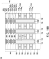
- Figures 21A through 21D are top-down views of amemory array 50, in accordance with some embodiments. Some features of an interconnect structure are illustrated.
- Figure 21A illustrates conductive vias at a first level of an interconnect structure (e.g., first-level conductive vias 162V 1 in Figures 19B and 19C ).
- Figure 21B illustrates conductive lines at a first level of an interconnect structure (e.g., first-level conductive lines 162L 1 in Figures 19B and 19C ).
- Figure 21C illustrates conductive vias at a second level of an interconnect structure (e.g., second-level conductive vias 162V 2 in Figures 19B and 19C ).
- Figure 21D illustrates conductive lines at a second level of an interconnect structure (e.g., second-level conductive lines 162L 2 in Figures 19B and 19C ).
- the conductive vias 162V 1 are over and connected to the bit lines 146B/source lines 146S.
- the bit lines 146B and the source lines 146S are formed in an alternating pattern along rows and columns of the memory array 50, in the top-down view. Forming the bit lines 146B and the source lines 146S in an alternating pattern helps avoid shorting of adjacent bit lines 146B/source lines 146S when a word line 114 (see Figures 19B and 19C) is activated.
- adjacent bit lines 146Band adjacent source lines 146S are laterally aligned with one another along the first direction D 1 (see Figures 1A and 1B ).
- the center of each conductive via 162V 1 is laterally aligned with the center of the respective underlying bit line 146B/source line 146S.
- the conductive lines 162L 1 are over and connected to the conductive vias 162V 1 .
- the conductive lines 162L 1 extend in the first direction D 1 (see Figures 1A and 1B ) and laterally offset the interconnection to the underlying bit lines/source lines.
- the conductive lines 162L 1 connected to the bit lines 146B are laterally offset from the conductive lines 162L 1 connected to the source lines 146S (see Figure 21A ) along the second direction D 2 (see Figures 1A and 1B ).
- the conductive vias 162V 2 are over and connected to theconductive lines 162L 1 . Because the conductive lines 162L 1 laterally offset the interconnection to the underlying bit lines/source lines, the center of each conductive via 162V 2 is thus laterally offset from the center of the respective underlying bit line/source line and from the center of the respective underlying conductive via 162V 1 .
- the conductive vias 162V 2 can be larger than (e.g., have greater widths than) the conductive vias 162V 1 .
- the conductive lines 162L 2 are over and connected to theconductivevias 162V 2 .
- the conductive lines 162L 2 include bit lineinterconnects 162B (which are connected to thebit lines 146B, see Figure 21A ) and source line interconnects 162S (which are connected to thesource lines 146S, see Figure 21A ). Because the conductive lines 162L 1 (see Figure 21C ) laterally offset the interconnection to the underlying bit lines/source lines, the bit lineinterconnects 162B and thesource line interconnects 162S can thus be straight conductive segments that extend in the second direction D 2 (see Figures 1A and 1B ).
- FIGS 22A through 22C are top-down view of memory cells, in accordance with various embodiments.
- the isolation regions 122 can have a width W 4 in the first direction D 1 (see Figures 1A and 1B ), which can be in the range of about 1 nm to about 100 nm.
- the back gate isolators 120 can have a width W 5 in the first direction D 1 , which can be in the range of about 1 nm to about 100 nm.
- the width W 5 is greater than the width W 4 in each illustrated embodiment.
- the semiconductor layers 118 can have a width W 6 in the first direction D 1 , which can be in the range of about 1 nm to about 100 nm.
- Figure 22A illustrates an embodiment where the semiconductor layers 118 were concurrently patterned with the patterning of the sacrificial regions 132/openings 140 (see Figure 15 ).
- the width W 6 is greater than the width W 5 .
- the width W 6 can be equal to the combined width W 7 of an isolation region 122, a source line 146S, and a bit line 146B.
- themain regions 146B M , 146S M of thebit lines 146B/source lines 146S are each separated from sidewalls of the memory films 116.
- Figure 22B illustrates an embodiment where the semiconductor layers 118were separately patterned after the patterning of the back gate isolators 120/openings 136 (see Figure 13) but before there deposition of the material of the sacrificial regions 132 in the openings 136 (see Figure 14 ) or the patterning of the sacrificial regions 132/openings 140 (see Figure 15 ).
- the width W 6 is greater than the width W 5 .
- the width W 6 is less than the combined width W 7 of an isolation region 122, a source line 146S, and a bit line 146B.
- themain regions 146B M , 146S M of thebit lines 146B/source lines 146S each contact a sidewall ofa memory film116 and a plurality of sidewalls of a semiconductor layer118.
- Figure 22C illustrates an embodiment where the semiconductor layers 118were concurrently patterned with the patterning of the back gate isolators 120/openings 136 (see Figure 13).
- the width W 6 is equal to the width W 5 .
- the width W 6 is less than the combined width W 7 of an isolation region 122, a source line 146S, and a bit line 146B.
- themain regions 146B M , 146S M of thebit lines 146B/source lines 146S each contact a sidewall ofa memory film116 and a single sidewall of a semiconductor layer118.
- Figure 23 is a cross-section view of a memory array 50, in accordance with some other embodiments.
- Figure 23 is shown along a similar cross-section as Figure 20B .
- the memory films 116 are formed of a plurality oflow-k dielectric layers. Specifically, eachof the memory films 116 includes a firstsub-layer 116L 1 , a second sub-layer 116L 2 on the first sub-layer 116L 1 , and a thirdsub-layer 116L 3 on the secondsub-layer 116L 2 .
- the first sub-layer 116L 1 and the third sub-layer 116L 3 are formed of a first dielectric material (e.g., an oxide such as silicon oxide) and the second sub-layer 116L 2 is formed of a different second dielectric material (e.g., a nitride such as silicon nitride).
- the low-k dielectric layers allow the transistors to act as floating gate transistors.
- the memory array 50 is formed over a substrate 102.
- the memory array 50 is formed as part of a standalone device (e.g., a memory die), which is integrated with other devices (e.g., a logic die) through devicepackaging.
- the memory array 50 is embedded in another device, such as a logic die.
- the substrate 102 may be omitted, or may be an underlying layer, such as an underlying dielectric layer, an underlying semiconductor substrate, or the like.
- Figure 24 is a cross-sectional view of a semiconductor device 300, in accordance with some embodiments.
- Figure 24 is a cross-sectional view shown along reference cross-section B-B' in Figure 1A .
- Figure 24 is a simplified view, and some features are omitted for clarity of illustration.
- the semiconductor device 300 includes a logic region 300L and a memory region 300M.
- Memory devices e.g., memories
- logic devices e.g., logic circuits
- a memory array 50 can be formed in the memory region 300M
- logic devices can be formed in the logic region 300L.
- the memory region 300M can be disposed at an edge of the logic region 300L, or the logic region 300L can surround the memory region 300M.
- the logic region 300L and the memory region 300M are formed over a same semiconductor substrate 302.
- the semiconductor substrate 302 may be silicon, doped or undoped, or an active layer of a semiconductor-on-insulator (SOI) substrate.
- the semiconductor substrate 302 may include other semiconductor materials, such as germanium; a compound semiconductor including silicon carbide, gallium arsenic, gallium phosphide, gallium nitride, indium phosphide, indium arsenide, and/or indium antimonide; an alloy semiconductor including SiGe, GaAsP, AlInAs, AlGaAs, GaInAs, GaInP, and/or GaInAsP; or combinations thereof.
- Other substrates, such as multilayered or gradient substrates, may also be used.
- Devices 304 are formed at the active surface of the semiconductor substrate 302.
- the devices 304 may be active devices or passive devices.
- the electrical components may be transistors, diodes, capacitors, resistors, or the like, formed by any suitable formation method.
- the devices 304 are interconnected to form the memory devices and logic devices of the semiconductor device 300.
- ILD layer(s) 306 are formed on the semiconductor substrate 302, and electrically conductive features, such as contact plugs 308, are formed electrically connected to the devices 304.
- the ILD layer(s) 306 may be formed of any suitable dielectric material, for example, a an oxide such as silicon oxide, phosphosilicate glass (PSG), borosilicate glass (BSG), boron-doped phosphosilicate glass (BPSG), or the like; nitride such as silicon nitride; or the like.
- the ILD layer(s) may be formed by any acceptable deposition process, such as spin coating, physical vapor deposition (PVD), chemical vapor deposition (CVD), the like, or a combination thereof.
- the electrically conductive features in the ILD layer(s) may be formed through any suitable process, such as deposition, damascene (e.g., single damascene, dual damascene, etc.), the like, or combinations thereof.
- An interconnect structure 310 is formed over the semiconductor substrate 302.
- the interconnect structure 310 interconnects the devices 304 to form integrated circuits in each of the logic region 300L and memory region 300M.
- the interconnect structure 310 includes multiple metallization layers M1-M5. Although five metallization layers are illustrated, it should be appreciated that more or less metallization layers may be included.
- Each of the metallization layers M1-M5 includes metallization patterns in dielectric layers.
- the metallization patterns are connectedto the devices 304 of the semiconductor substrate 302, and include, respectively, metal lines L1-L5 and metal vias V1-V5 formed in one or more inter-metal dielectric (IMD) layers.
- IMD inter-metal dielectric
- the interconnect structure 310 may formed by a damascene process, such as a single damascene process, a dual damascene process, or the like.
- the contact plugs 308 are also part of the metallization patterns, such as part of the lowest layer of metal vias VI.
- the memory array 50 is formed in the interconnect structure 310.
- the memory array 50 can be formed in any of the metallization layers M1-M5, and is illustrated as being formed in an intermediate metallization layer M4, although it could also be formed in lower metallization layers M1-M3 or an upper metallization layer M5.
- the memory array 50 is electrically connected to the devices 304.
- a metallization layer overlying the memory array 50 e.g., the metallization layer M5 contains interconnects to the source lines146S and the bit lines146B.
- the metallization layer overlying the memory array 50 can also contain interconnects to the word lines 114, such as through the conductive contacts 166 (see Figure 20J ).
- a metallization layer underlying the memory array 50 e.g., the metallization layer M3 contains interconnects to the source lines146S, the bit lines146B, and/or the word lines 114.
- the interconnect structure 310 may be formed by first forming the layers underlying the memory array 50, e.g., the metallization layers M1-M3.
- the memory array 50 can then be formed on the metallization layer M3, with the substrate 102 being an etch stop layer on the IMD of the metallization layer M3.
- the remainder of the metallization layer M4 can be formed, such as by depositing and planarizing the IMD for the metallization layer M4, and then forming metal lines M4 and metal vias M4 (which may include forming the IMD 216 and the conductive contacts 166, see Figure 20J ).
- the layers (if any) overlying the memory array 50, e.g., the metallization layer M5, can then be formed.
- Figures 25 through 27 are views of intermediate stages in the manufacturing of a memory array 50, in accordance with some other embodiments.
- Figures 25 through 27 are three-dimensional views.A portion of the memory array 50 is illustrated. Some features, such as the staircase arrangement of the word lines (see Figure 1A ), are not shown in some figures for clarity of illustration.
- a substrate 102 is provided and a multilayer stack 104 is formed over the substrate 102.
- Thesubstrate 102 and the multilayer stack 104 may be formed in a similar manner as those discussed above with respect to Figure 2 , except in this embodiment, themultilayer stack 104 includes alternating dielectric layers 106 and conductive layers 168.
- the conductive layers 168 may be formed of materials that are selected from the same group of candidate materials of the main layers 114A M ,114B M of the conductive features 114A, 114B, which may be formed using methods that are selected from the same group of candidate methods for forming the materialsof the main layers 114A M ,114B M of the conductive features 114A, 114B.
- trenches 110 are patterned in the multilayer stack 104.
- the trenches 110 may be formed in a similar manner as those discussed above with respect to Figure 3 .
- forming the trenches 110 patterns the conductive layers 168 to form word lines 114.
- the word lines 114 in this embodiment may not include multiple layers, but instead can each be a continuous layer of a conductive material (e.g., tungsten).
- thememory films 116, the semiconductor layers 118, the back gate isolators 120, and the isolation regions 122 are formed in the trenches 110. These features may be formed in a similar manner as those discussed above with respect to Figure 6 . Thefeatures of the transistors are thus formed by a single patterning process, in which only patterning process is used to form the trenches 110 and the layers of the transistors in themultilayer stack 104. After this step of processing, portions of the isolation regions 122 may bereplaced with the remaining features of the transistors, as discussed above with respect to Figures 11 through 18 . An interconnect structurecan then be formed, in a similar manner as that discussed above with respect to Figure 19A , 19B , and 19C .
- Embodiments may achieve advantages.
- the patternedback gate isolators 120 allow the extension regions 146B E , 146S E of the bit lines 146B/source lines 146S to also act as back gates duringwrite operations.
- Theback gates can help control (e.g., reduce) the surface potential of the semiconductor layers 118 (particularly the portions of the semiconductor layers 118 distal the word lines 114) duringwrite operations.
- the window for write operations may thus be widened. Reducing the surface potential of the semiconductor layers 118 during write operations also helps increase the write voltage that is applied across the memory films 116 during write operations. The performance of the memory array 50 may thus be improved.
- a device in an embodiment, includes:a word line extending in a first direction; a data storage layer on a sidewall of the word line; a channel layer on a sidewall of the data storage layer; a back gate isolator on a sidewall of the channel layer; and a bit line having a first main region and a first extension region, the first main region contacting the channel layer, the first extension region separated from the channel layer by the back gate isolator, the bit line extending in a second direction, the second direction perpendicular to the first direction.
- the first main region of the bit line is separated from the sidewall of the data storage layer by the channel layer. In some embodiments of the device, the first main region of the bit line contacts the sidewall of the data storage layer and a single sidewall of the channel layer. In some embodiments of the device, the first main region of the bit line contacts the sidewall of the data storage layer and a plurality of sidewalls of the channel layer. In some embodiments, the device further includes:a source line having a second main region and a second extension region, the second main region contacting the channel layer, the second extension region separated from the channel layer by the back gate isolator, the source line extending in the second direction; and an isolation region between the source line and the bit line.
- the isolation region, the first extension region of the bit line, and the second extension region of the source line have a same width in a third direction, the third direction perpendicular to the first direction and the second direction.
- the isolation region has a first width in the first direction and the back gate isolator has a second width in the first direction, the second width greater than the first width.
- the back gate isolator includes aluminum oxide.
- a device in an embodiment, includes:a bit line extending in a first direction, the bit line having a first T-shaped cross-section in a top-down view; a source line extending in the first direction, the source line having a second T-shaped cross-section in the top-down view;an isolation region between the source line and the bit line; a word line extending in a second direction, the second direction perpendicular to the first direction; a back gate isolator between the word line and each of the isolation region, a first portion of the bit line, and a second portion of the source line;a channel layer between the back gate isolator and the word line; anda data storage layer between the channel layer and the word line.
- the isolation region has a first width in the second direction
- the back gate isolator has a second width in the second direction, the second width greater than the first width
- the channel layer has the second width in the second direction.
- the channel layer has a third width in the second direction, and a combination of the bit line, the source line, and the isolation region has a fourth width in the second direction, the third width greater than the second width and less than the fourth width.
- the channel layer has a third width in the second direction, and a combination of the bit line, the source line, and the isolation region has the third width in the second direction, the third width greater than the second width.
- the device further includes:a source line interconnect over and connected to the source line; anda bit line interconnect over and connected to the bit line.
- the back gate isolator includes aluminum oxide.
- a method includes:forming a word line between a pair of first dielectric layers;depositing a data storage layer on sidewalls of the first dielectric layers and a sidewall of the word line;depositing a channel layer on a sidewall of the data storage layer;depositing a first dielectric layer on a sidewall of the channel layer;forming a first isolation region on a sidewall of the first dielectric layer;removing a first portion of the first isolation region, a second portion of the first isolation region remaining after the removing;after removing the first portion of the first isolation region, patterning the first dielectric layer to form a back gate isolator; and forming a bit line and a source line at opposing sides of the second portion of the first isolation region, the back gate isolator separating the channel layer from a first portion of the bit line and a second portion of the source line.
- the method further includes:patterning the channel layer while patterning the first dielectric layer. In some embodiments, the method further includes:forming a second isolation region extending through the channel layer; and patterning the channel layer while forming the second isolation region. In some embodiments, the method further includes:forming a second isolation region extending through the channel layer; and patterning the channel layer after patterning the first dielectric layer and before forming the second isolation region. In some embodiments of the method, the first dielectric layer is formed of aluminum oxide.
Landscapes
- Semiconductor Memories (AREA)
- Non-Volatile Memory (AREA)
- Metal-Oxide And Bipolar Metal-Oxide Semiconductor Integrated Circuits (AREA)
- Ultra Sonic Daignosis Equipment (AREA)
Abstract
In an embodiment, a device includes: a word line extending in a first direction; a data storage layer on a sidewall of the word line; a channel layer ona sidewall of the data storage layer; a back gate isolator ona sidewall of the channel layer; and a bit line having a first main region and a first extension region, the first main region contacting the channel layer, the first extension region separated from the channel layer by the back gate isolator, the bit lineextending in a second direction, the second direction perpendicular to the first direction.
Description
- Semiconductor memories are used in integrated circuits for electronic applications, including radios, televisions, cell phones, and personal computing devices, as examples. Semiconductor memories include two major categories. One is volatile memories; the other is non-volatile memories. Volatile memories include random access memory (RAM), which can be further divided into two subcategories, static random access memory (SRAM) and dynamic random access memory (DRAM). Both SRAM and DRAM are volatile because they will lose the information they store when they are not powered.
- On the other hand, non-volatile memories can keep data stored on them. One type of non-volatile semiconductor memory is ferroelectric random access memory (FeRAM). Advantages of FeRAM include its fast write/read speed and small size.
- Aspects of the present disclosure are best understood from the following detailed description when read with the accompanying figures. It is noted that, in accordance with the standard practice in the industry, various features are not drawn to scale. In fact, the dimensions of the various features may be arbitrarily increased or reduced for clarity of discussion.
-
Figures 1A ,1B , and1C are various views of a memory array. -
Figures 2 through 19C are various views of intermediate stages in the manufacturing of a memory array, in accordance with some embodiments. -
Figures 20A through 20J are views of intermediate stages in the manufacturing of a staircase structure of a memory array, in accordance with some embodiments. -
Figures 21A through 21D are top-down views of amemory array, in accordance with some embodiments. -
Figures 22A through 22C are top-down views of amemory array, in accordance with some embodiments. -
Figure 23 is a cross-section view of a memory array, in accordance with some other embodiments. -
Figure 24 is a cross-sectional view of a semiconductor device, in accordance with some embodiments. -
Figures 25 through 27 are various views of intermediate stages in the manufacturing of a memory array, in accordance with some other embodiments. - The following disclosure provides many different embodiments, or examples, for implementing different features of the invention. Specific examples of components and arrangements are described below to simplify the present disclosure. These are, of course, merely examples and are not intended to be limiting.For example, the formation of a first feature over or on a second feature in the description that follows may include embodiments in which the first and second features are formed in direct contact, and may also include embodiments in which additional features may be formed between the first and second features, such that the first and second features may not be in direct contact. In addition, the present disclosure may repeat reference numerals and/or letters in the various examples. This repetition is for the purpose of simplicity and clarity and does not in itself dictate a relationship between the various embodiments and/or configurations discussed.
- Further, spatially relative terms, such as "beneath," "below," "lower," "above," "upper" and the like, may be used herein for ease of description to describe one element or feature's relationship to another element(s) or feature(s) as illustrated in the figures. The spatially relative terms are intended to encompass different orientations of the device in use or operation in addition to the orientation depicted in the figures. The apparatus may be otherwise oriented (rotated 90 degrees or at other orientations) and the spatially relative descriptors used herein may likewise be interpreted accordingly.
- According to various embodiments, a three-dimensional memory array is formed of transistors (such as programmable thin film transistors (TFTs)) having source lines and bit lines with extension regions. The extension regions function as back gates. The data storage layers and channel layers of the transistors are disposed between the back gates and the word lines for the transistors. During a write operation (e.g., an erase or programming operation) for a transistor,theback gates can help control (e.g., reduce) the surface potential of the channel layers.Reducing the surface potential of the channel layers can help improve the performance of the memory array.
-
Figures 1A ,1B , and1C illustrate examples of amemory array 50, according to some embodiments.Figure 1A illustrates an example of a portion of thememory array 50 in a three-dimensional view;Figure 1B illustrates a circuit diagram of thememory array 50; andFigure 1C illustrates a top down view of a portion of thememory array 50. Thememory array 50 includes a plurality ofmemory cells 52, which may be arranged in a grid of rows and columns. Thememory cells 52 may further stacked vertically to provide a three dimensional memory array, thereby increasing device density. Thememory array 50 may be disposed in the back end of line (BEOL) of a semiconductor die. For example, thememory array 50 may be disposed in the interconnect layers of the semiconductor die, such as, above one or more active devices (e.g., transistors) formed on a semiconductor substrate. - In some embodiments, the
memory array 50 is a memory array such as a NOR memory array, or the like. Eachmemory cell 52 may include a transistor 54(such as a TFT) with an insulating,memory film 84 as a gate dielectric. In some embodiments, a gate of eachtransistor 54 is electrically coupled to a respective word line (e.g., conductive line 72), a first source/drain region of eachtransistor 54 is electrically coupled to a respective bit line (e.g.,conductive line 64B), and a second source/drain region of eachtransistor 54 is electrically coupled to a respective source line (e.g.,conductive line 64S), which electrically couples the second source/drain region to ground. Thememory cells 52 in a same horizontal row of thememory array 50 may share a common word line while thememory cells 52 in a same vertical column of thememory array 50 may share a common source line and a common bit line. - The
memory array 50 includes a plurality of vertically stacked conductive lines 72 (e.g., word lines) withdielectric layers 62 disposed between adjacent ones of theconductive lines 72. Theconductive lines 72 extend in a direction D1 parallel to a major surface of an underlying substrate (not explicitly illustrated inFigures 1A and1B ). Theconductive lines 72 may be part of a staircase structure such that lowerconductive lines 72 are longer than and extend laterally past endpoints of upperconductive lines 72. For example, inFigure 1A , multiple, stacked layers ofconductive lines 72 are illustrated with topmostconductive lines 72 being the shortest and bottommostconductive lines 72 being the longest. Respective lengths of theconductive lines 72 may increase in a direction towards the underlying substrate. In this manner, a portion of each of theconductive lines 72 may be accessible from above thememory array 50, and conductive contacts 66 (seeFigure 1C ) may be made to an exposed portion of each of theconductive lines 72. Theconductive contacts 66 may be, e.g., vias that connect the exposed portions of theconductive lines 72 to interconnects 68(seeFigure 1C ) of overlying interconnect layers, in embodiments where thememory array 50 is disposed in the interconnect layers of a semiconductor die. - The
memory array 50 further includes a plurality ofconductive lines 64B (e.g., bit lines) andconductive lines 64S (e.g., source lines). Theconductive lines conductive lines 72.Isolation regions 74 are disposed between and isolate adjacent ones of theconductive lines 64B and theconductive lines 64S. Pairs of theconductive lines conductive line 72 define boundaries of eachmemory cell 52, andanisolation region 76 is disposed between and isolates adjacent pairs of theconductive lines conductive lines 64S are electrically coupled to ground. AlthoughFigure 1A illustrates a particular placement of theconductive lines 64B relative theconductive lines 64S, it should be appreciated that the placement of theconductive lines - The
memory array 50 may also includesemiconductor layers 82. Thesemiconductor layers 82 may provide channel regions for thetransistors 54 of thememory cells 52. For example, when an appropriate voltage (e.g., higher than a respective threshold voltage (Vth) of a corresponding transistor 54) is applied through a correspondingconductive line 72, a region of asemiconductor layer 82 that intersects theconductive line 72 may allow current to flow from theconductive lines 64B to theconductive lines 64S (e.g., in the direction indicated by arrow 56). - A
memory film 84 is disposed between theconductive lines 72 and thesemiconductor layers 82, and thememory film 84 may provide gate dielectrics for thetransistors 54. In some embodiments, thememory film 84 comprises a ferroelectric material, such as a hafnium oxide, hafnium zirconium oxide, silicon-doped hafnium oxide, or the like. Accordingly, thememory array 50 may also be referred to as a ferroelectric random access memory (FERAM) array. Alternatively, thememory film 84 may be a multilayer structure comprising a layer of silicon nitride between two silicon oxide layers (e.g., an oxide-nitride-oxide (ONO) structure), a different ferroelectric material, a different type of memory layer (e.g., capable of storing a bit), or the like. - In embodiments where the
memory film 84 comprises a ferroelectric material, thememory film 84 may be polarized in one of two different directions, and the polarization direction may be changed by applying an appropriate voltage differential across thememory film 84 and generating an appropriate electric field. The polarization may be relatively localized (e.g., generally contained within each boundaries of the memory cells 52), and a continuous region of thememory film 84 may extend across a plurality ofmemory cells 52. Depending on a polarization direction of a particular region of thememory film 84, a threshold voltage of a corresponding transistor54 varies, and a digital value (e.g., 0 or 1) can be stored.For example, when a region of thememory film 84 has a first electrical polarization direction, the corresponding transistor54 may have a relatively low threshold voltage, and when the region of thememory film 84 has a second electrical polarization direction, the corresponding transistor54 may have a relatively high threshold voltage.The difference between the two threshold voltages may be referred to as the threshold voltage shift.A larger threshold voltage shift makes it easier (e.g., less error prone) to read the digital value stored in thecorresponding memory cell 52. - To perform a write operation on a
memory cell 52 in such embodiments, a write voltage is applied across a portion of thememory film 84 corresponding to thememory cell 52. The write voltage can be applied, for example, by applying appropriate voltages to a corresponding conductive line 72 (e.g., the word line) and the correspondingconductive lines memory film 84, a polarization direction of the region of thememory film 84 can be changed. As a result, the corresponding threshold voltage of the corresponding transistor54 can also be switched from a low threshold voltage to a high threshold voltage or vice versa, and a digital value can be stored in thememory cell 52. Because theconductive lines 72 intersect theconductive lines individual memory cells 52 may be selected for the write operation. - To perform a read operation on the
memory cell 52 in such embodiments, a read voltage (a voltage between the low and high threshold voltages) is applied to the corresponding conductive line 72 (e.g., the world line). Depending on the polarization direction of the corresponding region of thememory film 84, the transistor54 of thememory cell 52 may or may not be turned on. As a result, theconductive line 64B may or may not be discharged through theconductive line 64S (e.g., a source line that is coupled to ground), and the digital value stored in thememory cell 52 can be determined. Because theconductive lines 72 intersect theconductive lines individual memory cells 52 may be selected for the read operation. -
Figure 1A further illustrates reference cross-sections of thememory array 50 that are used in later figures. Cross-section B-B' is along a longitudinal axis ofconductive lines 72 and in a direction D1, for example, parallel to the direction of current flow of thetransistors 54. Cross-section C-C' is perpendicular to cross-section B-B' and in a direction D2, for example, perpendicular to a longitudinal axis of theconductive lines 72. Subsequent figures refer to these reference cross-sections for clarity. -
Figures 2 through 19C are views of intermediate stages in the manufacturing of amemory array 50, in accordance with some embodiments. Each memory cell 52of thememory array 50 includes a transistor 54 (seeFigures 19B and19C ).Figures 2 ,3 ,4 ,5 ,6 ,7 ,8 ,9 ,10 ,11 ,12 ,13 ,14 ,15 ,16 ,17 ,18 , and19A are three-dimensional views.Figure 19B is a cross-sectional view shown along reference cross-section B-B' inFigure 1A .Figure 19C is a cross-sectional view shown along reference cross-section C-C inFigure 1A . A portion of thememory array 50 is illustrated. Some features, such as the staircase arrangement of the word lines (seeFigure 1A ), are not shown in some figures for clarity of illustration. - In
Figure2 , asubstrate 102 is provided. Thesubstrate 102 may be a semiconductor substrate, such as a bulk semiconductor, a semiconductor-on-insulator (SOI) substrate, or the like, which may be doped (e.g., with a p-type or an n-type dopant) or undoped. Thesubstrate 102 may be a wafer, such as a silicon wafer. Generally, a SOI substrate is a layer of a semiconductor material formed on an insulator layer. The insulator layer may be, for example, a buried oxide (BOX) layer, a silicon oxide layer, or the like. The insulator layer is provided on a substrate, typically a silicon or glass substrate. Other substrates, such as a multilayered or gradient substrate may also be used. In some embodiments, the semiconductor material of thesubstrate 102 may include silicon; germanium; a compound semiconductor including silicon carbide, gallium arsenide, gallium phosphide, indium phosphide, indium arsenide, and/or indium antimonide; an alloy semiconductor including silicon germanium, gallium arsenide phosphide, aluminum indium arsenide, aluminum gallium arsenide, gallium indium arsenide, gallium indium phosphide, and/or gallium indium arsenide phosphide; or combinations thereof. Thesubstrate 102 may include a dielectric material. For example, thesubstrate 102 may be a dielectric layer, or may include a dielectric layer on a semiconductor substrate. Acceptable dielectric materials for thesubstrate 102 include oxides such as silicon oxide or aluminum oxide; nitrides such as silicon nitride; carbides such as silicon carbide; the like; or combinations thereof such as silicon oxynitride, silicon oxycarbide, silicon carbonitride, silicon oxycarbonitride or the like. In some embodiments, thesubstrate 102 is formed of silicon carbide. - A
multilayer stack 104 is formed over thesubstrate 102. Themultilayer stack 104 includes alternatingdielectric layers 106 andsacrificial layers 108. Thedielectric layers 106 are formed of a first dielectric material, and thesacrificial layers 108 are formed of a second dielectric material. The dielectric materials may each be selected from the candidate dielectric materials of the substrate 102.Themultilayer stack 104 will be patterned in subsequent processing. As such, the dielectric materials of thedielectric layers 106 and thesacrificial layers 108 both have a high etching selectivity from the etching of the material of thesubstrate 102. The patterneddielectric layers 106 will be used to isolate subsequently formed transistors. The patternedsacrificial layers 108 may also be referred to as dummy layers, and will be selectively replaced with word lines for the transistors in subsequent processing. As such, the second dielectric material of thesacrificial layers 108 also has a high etching selectivity from the etching of the first dielectric material of the dielectric layers 106. In embodiments where thesubstrate 102 is formed of silicon carbide, thedielectric layers 106 can be formed of silicon oxide, and thesacrificial layers 108 can be formed of silicon nitride. Other combinations of dielectric materials having acceptable etching selectivity from one another may also be used. - Each layer of the
multilayer stack 104 may be formed by an acceptable deposition process such as chemical vapor deposition (CVD), atomic layer deposition (ALD), or the like. A thickness of each of the layers may be in the range of about 40 nm to about 50 nm. In some embodiments, thedielectric layers 106 are formed to a different thickness than thesacrificial layers 108. For example, the sacrificial layers 108can be formed to a greater thickness than the dielectric layers 106. In the illustrated embodiment, themultilayer stack 104 includes five of thedielectric layers 106 and four of thesacrificial layers 108. It should be appreciated that themultilayer stack 104 may include other quantities of thedielectric layers 106 and thesacrificial layers 108. Themultilayer stack 104 can have an overall height H1 in the range of about 1000 nm to about 10000 nm. - As will be discussed in greater detail below,
Figures 3 through 10 illustrate a process in which a multiple-patterning process is used to form some of the features of the transistors. The multiple-patterning process may be a double patterning process, a quadruple patterning process, or the like.Figures 3 through 10 illustrate a double patterning process. In a double patterning process,trenches 110A (seeFigure 3 ) are patterned in portions of themultilayer stack 104 with a first etching process, and features for a first subset of the transistors are formed in thetrenches 110A.Trenches 110B (seeFigure 7 ) are then patterned in other portions of themultilayer stack 104 with a second etching process, and features for a second subset of the transistors are formed in thetrenches 110B. Forming the features of the transistors with a multiple-patterning process allowseach patterning process to be performed with a low pattern density, which can help reduce defects while still allowing thememory array 50 to have sufficient memory cell density .Further, forming the features of the transistors with a multiple-patterning process also allows each patterned portion of themultilayer stack 104 to avoid having an excessively large aspect ratio, thereby improving the structural stability of the resulting memory array. As will be discussed in greater detail below (seeFigures 25 through 27 ), a single patterning process may also be used to form some of the features of the transistors. - In
Figure 3 ,trenches 110A are patterned in themultilayer stack 104. In the illustrated embodiment, thetrenches 110A extend through themultilayer stack 104 and expose thesubstrate 102. In another embodiment, thetrenches 110A extend through some but not all layers of themultilayer stack 104. Thetrenches 110A may be patterned using acceptable photolithography and etching techniques, such as with an etching process that is selective to the multilayer stack 104 (e.g., selectively removes the dielectric materials of thedielectric layers 106 and thesacrificial layers 108 at a faster rate than the material of the substrate 102). The etching may be any acceptable etch process, such as a reactive ion etch (RIE), neutral beam etch (NBE), the like, or a combination thereof. The etching may be anisotropic. In embodiments where thesubstrate 102 is formed of silicon carbide, thedielectric layers 106 are formed of silicon oxide, and thesacrificial layers 108 are formed of silicon nitride, thetrenches 110A can be formed by a dry etch using a fluorine-based gas (e.g., C4F6) mixed with hydrogen (H2) or oxygen (O2) gas. After the patterning, respective portions of themultilayer stack 104 are disposed between respective ones of thetrenches 110A. Each portion of themultilayer stack 104 has a width W1 in the second direction D2 (seeFigures 1A and1B ), which can be in the range of about 50 nm to about 500 nm. Further, each portion of themultilayer stack 104 is separated by a separation distance S1 in the second direction D2, which can be in the range of about 50 nm to about 200 nm. - In
Figure 4 , thetrenches 110A are expanded to form sidewall recesses 112A. Specifically, portions of the sidewalls of thesacrificial layers 108 exposed by thetrenches 110A are recessed from the portions of the sidewalls of thedielectric layers 106 exposed by thetrenches 110A to form the sidewall recesses 112A. Although sidewalls of thesacrificial layers 108 are illustrated as being straight, the sidewalls may be concave or convex. The sidewall recesses 112A may be formed by an acceptable etching process, such as one that is selective to the material of the sacrificial layers 108 (e.g., selectively removes the material of thesacrificial layers 108 at a faster rate than the material(s) of thedielectric layers 106 and the substrate 102). The etching may be isotropic. In embodiments where thesubstrate 102 is formed of silicon carbide, thedielectric layers 106 are formed of silicon oxide, and the sacrificial layers 108are formed of silicon nitride, thetrenches 110A can be expanded by a wet etch using phosphoric acid (H3PO4). In another embodiment, a dry etch selective to the material of the sacrificial layers 108may be used. - After formation, the sidewall recesses 112A have a depth D4 in the second direction D2 (see
Figures 1A and1B ), extending past the sidewalls of the dielectric layers 106. Timed etch processes may be used to stop the etching of the sidewall recesses 112A after the sidewall recesses 112A reach a desired depth D4. For example, the sidewall recesses 112Acan have a depth D4 in the range of about 10 nm to about 60 nm.Forming the sidewall recesses 112A can reduce the widths of thesacrificial layers 108 by about 5% to about 25%.Continuing the previous example, after the etching, thesacrificial layers 108 can have a width W2 in the second direction D2, which can be in the range of about 50 nm to about 450 nm. - In
Figure 5 ,conductive features 114A (e.g., metal lines) are formed in the sidewall recesses 112A, thus completing a process for replacing first portions of thesacrificial layers 108. The conductive features 114A may each include one or more layers, such as seed layers, glue layers, barrier layers, diffusion layers, fill layers, and the like. In some embodiments, theconductive features 114A each include aseed layer 114AS (or barrier layer) and amain layer 114AM. Eachseed layer 114AS extends along three sides (e.g., the top surface, a sidewall, and the bottom surface) of a correspondingmain layer 114AM located within a correspondingsidewall recesses 112A. The seed layers 114AS are formed of a first conductive materialthat can be utilized to help grow or to help adhere a subsequently deposited material, such as a metal nitride, such as titanium nitride, tantalum nitride, molybdenumnitride, zirconium nitride, hafnium nitride, or the like. Themainlayers 114AM may are formed of a second conductive material, such as a metal, such as tungsten, ruthenium, molybdenum,cobalt, aluminum, nickel,copper, silver, gold, alloys thereof, or the like. The material of theseed layers 114AS is one that has good adhesion to the material of thedielectric layers 106, and the material of themainlayers 114AM is one that has good adhesion to the material of the seed layers 114AS. In embodiments where thedielectric layers 106 are formed of an oxide such as silicon oxide, the seed layers 114AS can be formed of titanium nitride ortantalum nitride, and themainlayers 114AM can be formed of tungsten. Thematerials of the seed layers 114AS andmainlayers 114AM may be formed by acceptable deposition processes such as chemical vapor deposition (CVD), atomic layer deposition (ALD), or the like.An acceptable etch process, such as a dry etch (e.g., a reactive ion etch (RIE), neutral beam etch (NBE), the like), a wet etch, the like, or a combination thereof, may be performed to remove excess material from the sidewalls of thedielectric layers 106 and the top surface of thesubstrate 102. The etching may be anisotropic. Each of theconductive features 114A can have a similar overall thickness as the sacrificial layers 108 (discussed above forFigure 2 ), and can have a similar overall width as the depth D4 of the sidewall recesses 112A (discussed above forFigure 4 ).Eachseed layer 114AS can have a thickness in the range of about 1 nm to about 10 nm, and eachmain layer 114AM can have a thickness in the range of about 15 nm to about 35 nm, with the thickness oftheseed layer 114AS being greater than the thickness of themainlayer 114AM. - In
Figure 6 ,memory films 116A, semiconductor layers 118A, backgate isolators 120A, andisolation regions 122A are formed in thetrenches 110A. The semiconductor layers 118A and theback gate isolators 120A are formed overthememory films 116A.Theisolation regions 122A extend through the semiconductor layers 118A, thus separating the semiconductor layers 118A of horizontally adjacent transistors along the direction D2 (seeFigures 1A and1B ). In the illustrated embodiment, theisolation regions 122A are formed over thememory films 116A. In another embodiment, theisolation regions 122A also extend throughthememory films 116A and thesubstrate 102,thus separating thememory films 116A of horizontally adjacent transistors along the direction D2. - Portions of the
memory films 116A providedata storage layers for the transistors and portions of the semiconductor layers 118Aprovide channel regions for the transistors. As will be discussed in greater detail below, thebackgate isolators 120A will be patterned and used to help form T-shaped source/drain regionsof the transistors. The T-shaped source/drain regions have main regions and extension regions.Theback gate isolators 120A will be patterned so that themain source/drain regions may contact the semiconductor layers 118A, but thesource/drainextension regions are separated from the portions of thesemiconductor layers 118A thatprovidethe channel regions, thus preventing shorting of the channel regions. Thesource/drainextension regions can act as back gates to help control (e.g., reduce) the surface potential of the semiconductor layers 118 (particularly the portions of the semiconductor layers 118 distal the word lines 114) duringwrite operations.The window for write operations may thus be widened. - The memory films 116Aare formed of an acceptable material for storing digital values. In some embodiments, the
memory films 116A are formed of a high-k ferroelectric material, such ashafnium zirconium oxide (HfZrO); zirconium oxide (ZrO); hafnium oxide (HfO) doped with lanthanum (La), silicon (Si), aluminum (Al), or the like; undoped hafnium oxide (HfO); or the like. In some embodiments, thememory films 116A include one or more low-k dielectric materials, such as silicon nitride, silicon oxide, silicon oxynitride, or the like. The material ofthememory films 116A may be formed by an acceptable deposition process such as ALD, CVD, physical vapor deposition (PVD), or the like. In some embodiments, thememory films 116A are HfZrO deposited by ALD. - The semiconductor layers 118A formed of an acceptable material for providing channel regions for the transistors, such as indium gallium zinc oxide (IGZO), indium tin oxide (ITO), indium gallium zinc tin oxide (IGZTO), zinc oxide (ZnO), polysilicon, amorphous silicon, or the like. The material of the semiconductor layers 118A may be formed by an acceptable deposition process such as ALD, CVD, PVD, or the like.In some embodiments, the semiconductor layers 118Aare formed of IGZTO deposited by ALD.
- The
back gate isolators 120A are formed of an acceptable material for electrically insulating subsequently formed source/drainextension regions from the portions of thesemiconductor layers 118A thatprovide channel regions. In some embodiments, thebackgate isolators 120A are formed of a dielectric material. Acceptable dielectric materials for theback gate isolators 120A include oxides such as silicon oxide or aluminum oxide; nitrides such as silicon nitride; carbides such as silicon carbide; the like; or combinations thereof such as silicon oxynitride, silicon oxycarbide, silicon carbonitride, silicon oxycarbonitride or the like.The material of thebackgate isolators 120A may be formed by an acceptable deposition process such as ALD, CVD, flowable CVD (FCVD), or the like.In some embodiments, theback gate isolators 120A are formed of an oxide such as aluminum oxide deposited by ALD. - The
isolation regions 122A are formed of an acceptablematerial for protecting and electrically isolating theunderlyingmemory films 116A. Acceptable dielectric materials fortheisolation regions 122A include oxides such as silicon oxide or aluminum oxide; nitrides such as silicon nitride; carbides such as silicon carbide; the like; or combinations thereof such as silicon oxynitride, silicon oxycarbide, silicon carbonitride, silicon oxycarbonitride or the like. The material oftheisolation regions 122 may be formed by an acceptable deposition process such as ALD, CVD, flowable CVD (FCVD), or the like.Theisolation regions 122A andtheback gate isolators 120A are formed of different dielectric materials so that the material oftheisolation regions 122A has a high etching selectivity from the etching of the material of theback gate isolators 120A.In some embodiments, the isolation regions 122Aare formed of an oxide such as silicon oxide deposited by FCVD. - The
memory films 116A, the semiconductor layers 118A, theback gate isolators 120A, and theisolation regions 122A may be formed by a combination of deposition, etching, and planarization. For example, a tunneling layer can be conformally deposited onthemultilayer stack 104 and in thetrenches 110A (e.g., on the sidewalls of theconductive features 114A and the sidewalls of the dielectric layers 106). A semiconductor layer can then be conformally deposited on the tunneling layer. A dielectric layer can then be conformally deposited on the semiconductor layer. The dielectric layer can then be patterned bya suitable etching process, such as an anisotropicetch using the tunneling layer as an etch stop layer. Thesemiconductor layercan then be patterned bya suitable etching process, such as an anisotropicetchusing thepatterneddielectric layer as an etching mask. Anisolation material can then be conformally deposited in the remaining portions oftrenches 110A (e.g., on the patterned semiconductor layer, the patterneddielectric layer, and the exposed portions of the tunneling layer). A removal process is then applied to the various layers to remove excess materials over the topmostdielectric layers 106/sacrificial layers 108.The removal process may be a planarization process such as a chemical mechanical polish (CMP), an etch-back, combinations thereof, or the like.The portions of the tunneling layer, the semiconductor layer, the dielectric layer, and theisolation material remaining in thetrenches 110A forms thememory films 116A, the semiconductor layers 118A, theback gate isolators 120A, and theisolation regions 122A,respectively. The planarization process exposes the topmostdielectric layers 106/sacrificial layers 108 such that top surfaces of thememory films 116A, the semiconductor layers 118A, theback gate isolators 120A, theisolation regions 122A, and the topmostdielectric layers 106/sacrificial layers 108 are coplanar (within process variations) after the planarization process. - Optionally, the
isolation regions 122A can be formed to also extend through the throughthememory films 116A and the substrate 102.As will be discussed in greater detail below, in some embodiments, thememory array 50 is embedded in another semiconductor device. Specifically, thememory array 50 can be formed in the interconnect structure of a semiconductor device. In such embodiments, openings can be formed throughthememory films 116A and the substrate 102before depositing the isolation material oftheisolation regions 122A. Portions oftheisolation regions 122A will be subsequently replaced withsource/drain regions of the transistors so that the source/drain regions are connected to metallization layers of the interconnect structure that underlyunderlying thememory array 50. A suitable etching process can be performed on thememory films 116A and thesubstrate 102 using the semiconductor layers 118A and theback gate isolators 120A as an etching mask. The etching process is selective to thememory films 116A and the substrate 102 (e.g., selectively removes the material(s) of thememory films 116A and thesubstrate 102 at a faster rate than the material(s)the semiconductor layers 118A and theback gate isolators 120A).The etch may be anisotropic. In some embodiments, theetching process includes multiple etches. For example, a first etch can be performed to extend the openings through thememory films 116A, and a second etch can be performed to extend the openings through thesubstrate 102. After the openings are formed, theisolation regions 122A can be formed by a similar manner as described above. - In
Figure 7 ,trenches 110B are patterned in themultilayer stack 104. In the illustrated embodiment, thetrenches 110B extend through themultilayer stack 104 and expose thesubstrate 102. In another embodiment, thetrenches 110B extend through some but not all layers of themultilayer stack 104. Thetrenches 110B may be patterned using acceptable photolithography and etching techniques, such as with an etching process that is selective to the multilayer stack 104 (e.g., selectively removes the dielectric materials of thedielectric layers 106 and thesacrificial layers 108 at a faster rate than the material of the substrate 102). The etching may be any acceptable etch process, and in some embodiments, may be similar to the etch used to form thetrenches 110A (discussed above forFigure 3 ). - After the patterning, respective portions of the
multilayer stack 104 are disposed between respective pairs of thetrenches multilayer stack 104 has a width W3 in the second direction D2 (seeFigures 1A and1B ), which can be in the range of about 50 nm to about 500 nm. Further, each portion of themultilayer stack 104 is separated by a separation distance S2 in the second direction D2, which can be in the range of about 50 nm to about 200 nm.Misalignment may occur when patterning thetrenches 110B. When misalignment occurs, the patterned portions of themultilayer stack 104 do not all have a samewidth W3. When no misalignment occurs,the patterned portions of themultilayer stack 104 have a samewidth W3. - In
Figure 8 , thetrenches 110B are expanded to form sidewall recesses 112B. Specifically, the remaining portions of thesacrificial layers 108 are removed to form the sidewall recesses 112B. Thesidewall recesses 112B thus expose the sidewalls of theconductive features 114A(e.g., the sidewalls oftheseed layers 114AS). The sidewall recesses 112B may be formed by an acceptable etching process, such as one that is selective to the material of the sacrificial layers 108 (e.g., selectively removes the material of thesacrificial layers 108 at a faster rate than the material(s) of thedielectric layers 106 and thesubstrate 102).The etching may be any acceptable etch process, and in some embodiments, may be similar to the etch used to form the sidewall recesses 112A (discussed above forFigure 4 ). - After formation, the sidewall recesses 112B have a depth D5 in the second direction D2 (see
Figures 1A and1B ), extending past the sidewalls of the dielectric layers 106. Timed etch processes may be used to stop the etching of the sidewall recesses 112B after the sidewall recesses 112B reach a desired depth D5. As noted above,misalignment may occur when patterning thetrenches 110B. When misalignment occurs, the depth D5 is different from (e.g., greater than or less than) the depth D4 (discussed above forFigure 4 ). When no misalignment occurs, the depth D5 is similar to the depth D4. - In
Figure 9 , conductive features 114B are formed in the sidewall recesses 112B, thus completing a process for replacing second portions of thesacrificial layers 108. The conductive features 114B may be formed of materials that are selected from the same group of candidate materials of theconductive features 114A, which may be formed using methods that are selected from the same group of candidate methods for forming the materialsof theconductive features 114A. The conductive features 114A and theconductive features 114B may be formed from the same material, or may include different materials. In some embodiments, theconductive features 114B each include aseed layer 114BS(or barrier layer) and amain layer 114BM. The seed layers 114BS and themain layers 114BM can have similar thicknesses as the seed layers 114AS and themain layers 114AM, respectively. In some embodiments, the seed layers 114AS andtheseed layers 114BS are formed of similar materials, in which case the seed layers 114AS andtheseed layers 114BS may merge during formation such that no discernable interfaces exist between them. In another embodiment, the seed layers 114AS andtheseed layers 114BS are formed of different materials, in which case the seed layers 114AS andtheseed layers 114BS may not merge during formation such that discernable interfaces exist between them.As noted above,misalignment may occur when patterning thetrenches 110B. When misalignment occurs, themain layers 114AM have different widths from themain layers 114BM along the second direction D2 (seeFigures 1A and IB).When no misalignment occurs,the main layers 114AMhave the same width as themain layers 114BM along the second direction D2. Portions of eachseed layer main layer 114AM and amain layer 114BM. - The conductive features 114A and theconductive features 114B are collectively referred to as
word lines 114 of thememory array 50. Adjacent pairs of theconductive features 114A and theconductive features 114B are in physical contact with one another and are electrically coupled to one another. Thus, each pair ofconductive features single word line 114. - In
Figure 10 , thememory films 116B, semiconductor layers 118B, backgate isolators 120B, andisolation regions 122B are formed in thetrenches 110B. The semiconductor layers 118B and theback gate isolators 120B are formed overthememory films 116B.Theisolation regions 122B extend through the semiconductor layers 118B, thus separating the semiconductor layers 118B of horizontally adjacent transistors along the direction D2 (seeFigures 1A and1B ). In the illustrated embodiment, theisolation regions 122B are formed over thememory films 116B. In another embodiment, theisolation regions 122B also extend through thememory films 116Band thesubstrate 102,thus separating thememory films 116B of horizontally adjacent transistors along the direction D2. - The
memory films 116B may be formed of a material that is selected from the same group of candidate materials of thememory films 116A, which may be formed using a method that is selected from the same group of candidate methods for forming the material of thememory films 116A. Thememory films 116A and thememory films 116B may be formed from the same material, or may include differentmaterials.Thememory films 116A and thememory films 116B are collectively referred to as memory films 116.A thickness of the memory films 116can be in the range of about 2 nm to about 20 nm. - The semiconductor layers 118B may be formed of a material that is selected from the same group of candidate materials of the semiconductor layers 118A, which may be formed using a method that is selected from the same group of candidate methods for forming the material of the semiconductor layers 118A. The semiconductor layers 118A and the semiconductor layers 118B may be formed from the same material, or may include different materials. Thesemiconductor layers 118A and the semiconductor layers 118B are collectively referred to as semiconductor layers 118.A thickness of the semiconductor layers 118can be in the range of about 9 nm to about 11 nm.
- The
back gate isolators 120B may be formed of a material that is selected from the same group of candidate materials of theback gate isolators 120A, which may be formed using a method that is selected from the same group of candidate methods for forming the material of theback gate isolators 120A. Theback gate isolators 120A and theback gate isolators 120B may be formed from the same material, or may include different materials.Theback gate isolators 120A and theback gate isolators 120B are collectively referred to as back gate isolators 120.A thickness of the back gate isolators 120can be in the range of about 1 nm to about 20 nm. - The
isolation regions 122B may be formed of a material that is selected from the same group of candidate materials of theisolation regions 122A, which may be formed using a method that is selected from the same group of candidate methods for forming the material of theisolation regions 122A. Theisolation regions 122A and theisolation regions 122B may be formed from the same material, or may include different materials. Theisolation regions 122B andtheback gate isolators 120B are formed of different dielectric materials so that the material oftheisolation regions 122B has a high etching selectivity from the etching of the material of theback gate isolators120B.Theisolation regions 122A and theisolation regions 122B are collectively referred to as isolation regions 122.A thickness of theisolation regions 122 can be in the range of about 42 nm to about 192 nm. - The
memory films 116B, the semiconductor layers 118B, theback gate isolators 120B, and theisolation regions 122B may be formed by a combination of deposition, etching, and planarization. For example, thememory films 116B, the semiconductor layers 118B, theback gate isolators 120B, and theisolation regions 122B may be formed by similar steps (discussed above forFigure 6 ) as those used to form thememory films 116A, the semiconductor layers 118A, theback gate isolators 120A, and theisolation regions 122A. - As will be discussed in greater detail below,
Figures 11 through 18 illustrate a process in which portions of theisolation regions 122 are replaced with the remaining features of the transistors. Specifically, portions of theisolation regions 122 are replaced with isolation regions 142 (seeFigure 16 ), and withbit lines 146B andsource lines 146S (seeFigure 18 ). The remaining portions of theisolation regions 122 separate the features of horizontally adjacent transistorsalong the direction D1 (seeFigures 1A and1B ). The bit lines 146B and the source lines 146S also act as source/drain regions of the transistors. During the process for replacing the portions of theisolation regions 122, theback gate isolators 120 are patterned. Thepatternedback gate isolators 120 allow portions of the bit lines 146B/source lines 146S to also act as back gates duringwrite operations. - In
Figure 11 , portions oftheisolation regions 122 are removed to formopenings 130. Theopenings 130 may be formed with an etching process that is selective to the isolation regions 122 (e.g., selectively removes the material of theisolation regions 122 at a faster rate than the materials of thememory films 116 and the back gate isolators 120). The etching may be any acceptable etch process, such as a reactive ion etch (RIE), neutral beam etch (NBE), the like, or a combination thereof. The etching may be anisotropic. In embodiments where theisolation regions 122 are formed of silicon oxide, theopenings 130 can be formed through theisolation regions 122 by a dry etch using ammonia (NH3) and hydrogen fluoride (HF) gas, performed with an etching mask having a pattern of theopenings 130. - In
Figure 12 ,sacrificial regions 132 are formed in the openings 130.Thesacrificial regions 132 are formed of a sacrificial material, such as a dielectric material, which will be replaced with bit lines and source lines in subsequent processing. As such, the dielectric material of thesacrificial regions 132 has a high etching selectivity from the etching of the materials of thememory films 116, the semiconductor layers 118, and theback gate isolators 120. Acceptable dielectric materials for thesacrificial regions 132 include oxides such as silicon oxide or aluminum oxide; nitrides such as silicon nitride; carbides such as silicon carbide; the like; or combinations thereof such as silicon oxynitride, silicon oxycarbide, silicon carbonitride, silicon oxycarbonitride or the like. The material of thesacrificial regions 132 may be formed by an acceptable deposition process such as ALD, CVD, flowable CVD (FCVD), or the like.In some embodiments, thesacrificial regions 132 are formed of a nitride such as silicon nitride deposited by CVD.A removal process may be applied to the material of thesacrificial regions 132 to remove excess of the material over the topmostdielectric layers 106/sacrificial layers 108.The removal process may be a planarization process such as a chemical mechanical polish (CMP), an etch-back, combinations thereof, or the like.The planarization process exposes the topmostdielectric layers 106/sacrificial layers 108 such that top surfaces of the sacrificial regions 132and the topmostdielectric layers 106/sacrificial layers 108 are coplanar (within process variations) after the planarization process. - In
Figure 13 , theback gate isolators 120 and thesacrificial regions 132 are patterned to formopenings 136. Theopenings 136 may be formed with an etching process that is selective to theback gate isolators 120 and the sacrificial regions 132 (e.g., selectively removes the materials of theback gate isolators 120 and thesacrificial regions 132 at a faster rate than the materials of the semiconductor layers 118 and/or the memory films 116). The etching may be any acceptable etch process, such as a reactive ion etch (RIE), neutral beam etch (NBE), the like, or a combination thereof. The etching may be anisotropic. In embodiments where theback gate isolators 120 are formed of aluminum oxide and thesacrificial regions 132 are formed of silicon nitride, theopenings 136 can be formed through theback gate isolators 120 and thesacrificial regions 132 bya dry etch using a fluorine-based gas (e.g., C4F6) mixed with hydrogen (H2) or oxygen (O2) gas, performed with an etching mask having a pattern of theopenings 136. - In
Figure 14 , additional material of thesacrificial regions 132 is redeposited in theopenings 136 to reform thesacrificial regions 132. Eachsacrificial region 132 thus hasfirst portions 132A and asecond portion 132B. As noted above,thesacrificial regions 132 will be replaced with bit lines and source lines in subsequent processing, and the bit lines/source lines will have main regions and extension regions. Thefirst portions 132A of the sacrificial region 132correspond to the portions of the sacrificial material that were not removed when forming theopenings 136, and will be replaced with the extension regions of thebit lines/source lines. Thesecond portions 132B of the sacrificial region 132correspond to the portions of the sacrificial material that were redeposited in theopenings 136, and will be replaced with the main regionsof thebit lines/source lines. Theportions sacrificial regions 132 may merge during redeposition such that no discernable interfaces exist between them. - In
Figure 15 ,openings 140 for isolation regions are formed through thesacrificial regions 132. Theopenings 140 divide thesacrificial regions 132 into portions that will be replaced with bit lines and source linesin subsequent processing. Theopenings 140 may be formed with an etching process that is selective to the sacrificial regions 132 (e.g., selectively removes the material of thesacrificial regions 132 at a faster rate than the material of the memory films 116). The etching may be any acceptable etch process, such as a reactive ion etch (RIE), neutral beam etch (NBE), the like, or a combination thereof. The etching may be anisotropic. In embodiments where thesacrificial regions 132 are formed of silicon nitride, theopenings 140 can be formed through thesacrificial regions 132 by a dry etch using a fluorine-based gas (e.g., C4F6) mixed with hydrogen (H2) or oxygen (O2) gas, performed with an etching mask having a pattern of theopenings 140. - The semiconductor layers 118 are patterned during processing so that the semiconductor layers 118 of horizontally adjacent transistors are separated along the direction D1 (see
Figures 1A and1B ). As will be discussed in greater detail below, the semiconductor layers 118 can be patterned at one of several steps during processing, depending on the desired widths of the divided semiconductor layers 118. In this embodiment, the semiconductor layers 118 are concurrently patterned with the patterning of thesacrificial regions 132/openings 140 (seeFigure 15 ). In another embodiment, the semiconductor layers 118are concurrently patterned with the patterning of theback gate isolators 120/openings 136 (seeFigure 13). In yet another embodiment, the semiconductor layers 118are patterned in a separate step after the patterning of theback gate isolators 120/openings 136 (seeFigure 13) but before there deposition of the material of thesacrificial regions 132 in the openings 136 (seeFigure 14 ) or the patterning of thesacrificial regions 132/openings 140 (seeFigure 15 ). When they are separately patterned, the semiconductor layers 118may be patterned with an etching process that is selective to the semiconductor layers 118(e.g., selectively removes the material of the semiconductor layers 118at a faster rate than the material of the memory films 116). The etching may be any acceptable etch process, such as a reactive ion etch (RIE), neutral beam etch (NBE), the like, or a combination thereof. The etching may be anisotropic. In embodiments where the semiconductor layers 118 are formed of IGZTO, the semiconductor layers 118may be patterned bya dry etch using Cl2, BCl3, CF4, SF6, or the like. - In
Figure 16 ,isolation regions 142 are formed in theopenings 140. Theisolation regions 142 thus extend through thesacrificial regions 132. Theisolation regions 142 may be formed of a material that is selected from the same group of candidate materials of theisolation regions 122, which may be formed using a method that is selected from the same group of candidate methods for forming the material of theisolation regions 122. Theisolation regions 122 and theisolation regions 142 may be formed from the same material, or may include different materials. In some embodiments, theisolation regions 142 are formed of silicon oxide deposited by CVD. As an example to form theisolation regions 142, an isolation material is formed in theopenings 140. A removal process is then applied to the various layers to remove excess isolation material over the topmostdielectric layer 106/word line 114. The removal process may be a planarization process such as a chemical mechanical polish (CMP), an etch-back, combinations thereof, or the like. The remaining isolation material forms theisolation regions 142 in theopenings 140. - In
Figure 17 , thesacrificial regions 132 are removed to form openings 144.Theopenings 144 may be formed with an etching process that is selective to the sacrificial regions 132 (e.g., selectively removes the material of thesacrificial regions 132 at a faster rate than the materials of theisolation regions 142, theback gate isolators 120,theisolation regions 122,the semiconductor layers 118,and the memory films 116). The etching may be isotropic. In embodiments where thesacrificial regions 132 are formed of silicon nitride, theopenings 144 can be formed by a wet etch using phosphoric acid (H3PO4). In another embodiment, a dry etch selective to the material of thesacrificial regions 132 may be used. - In
Figure 18 , conductive lines (includingbit lines 146B andsource lines 146S) are formed in theopenings 144. The bit lines 146B and the source lines 146S are conductive pillars, and may also be referred to as bit line pillars and source line pillars. Each transistor will include abit line 146B and asource line 146S, withanisolation region 122 disposed betweenthebit line 146B and thesource line 146S. In this embodiment, the bit lines 146B/source lines 146S extend though the semiconductor layers 118. In another embodiment, the bit lines 146B/source lines 146S also extend through the memory films 116and thesubstrate 102. - As an example to form the bit lines 146B/
source lines 146S, a liner, such as a diffusion barrier layer, an adhesion layer, or the like, and a main layer are formed in theopenings 144. The liner may be formed of a conductive material such as titanium, titanium nitride, tantalum, tantalum nitride, or the like, which may be deposited by a conformal deposition process, such as atomic layer deposition (ALD), chemical vapor deposition (CVD), physical vapor deposition (PVD), or the like. In some embodiments, the liner may include an adhesion layer and at least a portion of the adhesion layer may be treated to form a diffusion barrier layer. The main layer may be formed of a conductive material such as tungsten, cobalt, ruthenium, aluminum, nickel, copper, a copper alloy, silver, gold, or the like, which may be deposited by ALD, CVD, PVD, or the like. In some embodiments, the bit lines 146B/source lines 146S include a liner formed of titanium nitride and a main layer formed of tungsten. A removal process is then applied to the various layers to remove excess material(s) of the bit lines 146B/source lines 146S over the topmostdielectric layers 106/word lines 114. The removal process may be a planarization process such as a chemical mechanical polish (CMP), an etch-back, combinations thereof, or the like. The remaining material(s) in theopenings 144 form the bit lines 146B/source lines 146S. The planarization process exposes the topmostdielectric layers 106/word lines 114 such that top surfaces of the bit lines 146B/source lines 146S, theisolation regions 142, theisolation regions 122, theback gate isolators 120, the semiconductor layers 118, thememory films 116, and the topmostdielectric layers 106/word lines 114 are coplanar (within process variations) after the planarization process. - Thebit lines 146B/
source lines 146S each have T-shaped cross-sections in the top-down view. Specifically, the bit lines 146B havemain regions 146BM that extend along the sidewalls of the semiconductor layers 118, and haveextension regions 146BE that extend along the sidewalls of thebackgate isolators 120. Similarly, the source lines 146S havemain regions 146SM that extend along the sidewalls of the semiconductor layers 118, and haveextension regions 146SE that extend along the sidewalls of thebackgate isolators 120. Theextension regions isolation regions 122 each have the same width in the second direction D2 (seeFigures 1A and1B ). The patterned backgate isolators 120 allow themainregions extension regions semiconductor layers 118 thatprovide channel regions. As such, theextension regions - In
Figures 19A ,19B , and19C , aninterconnect structure 160 is formed over the intermediate structure. Theinterconnect structure 160 may include, e.g.,metallization patterns 162 in a dielectric material 164 (not shown inFigure 19A , seeFigures 19B and19C ). Thedielectric material 164 may include one or more dielectric layers, such as one or more layers of a low-k (LK) or an extra low-K (ELK) dielectric material. Themetallization patterns 162 may be metal interconnects (e.g.,conductive lines 162L,conductive vias 162V, etc.) formed in thedielectric material 164. Theinterconnect structure 160 may be formed by a damascene process, such as a single damascene process, a dual damascene process, or the like.Themetallization patterns 162 of theinterconnect structure 160 are electrically connected to the bit lines 146B/source lines 146S, and interconnect thetransistors 54 to form functional memories. - As noted above, the
dielectric layers 106 and the word lines 114 may be formed in a staircase structure. Thedielectric layers 106 and the word lines 114 may be patterned to form the staircase structure at any suitable step before the formation of theinterconnect structure 160. Forming theinterconnect structure 160 includes forming conductive contacts that are connected to the exposed portions of each of the word lines 114. -
Figures 20A through 20J are views of intermediate stages in the manufacturing of a staircase structure of amemory array 50, in accordance with some embodiments.Figures 20A through 20J are cross-sectional views illustrated along reference cross-section B-B' illustrated inFigure 1A . Some features of the transistors, such as thememory films 116, the semiconductor layers 118, theback gate isolators 120, and the like (seeFigures 6 through 19C ), are not shown for clarity of illustration. InFigures 20A through 20J , themultilayer stack 104 is patterned to form a staircase structure after thesacrificial layers 108 are replaced with the word lines 114. It should be appreciated that the process shown may be performed at other suitable steps of processing. - In
Figure 20A amask 202 is formed over themultilayer stack 104. At this step of processing, themultilayer stack 104 comprises alternating dielectric layers 204 (such as thedielectric layers 106 discussed above, labeled 204A, 204B, 204C, 204D) and conductive layers 206 (such as the word lines 114 discussed above, labeled 206A, 206B, 206C). Themask 202 may be a photoresist or the like, which can be formed by a spin-on technique or the like. - In
Figure 20B , themask 202 is patterned to expose themultilayer stack 104 inregions 210A while masking remaining portions of the multilayer stack 104.For example, a topmost layer of the multilayer stack 104 (e.g., thedielectric layer 204D) may be exposed in theregions 210A. Themask 202 may be patterned using acceptable photolithography techniques - In
Figure 20C , the exposed portions of themultilayer stack 104 in theregions 210A are etched using themask 202 as an etching mask. The etching may be any acceptable etch process, such as by wet or dry etching, a reactive ion etch (RIE), neutral beam etch (NBE), the like, or a combination thereof. The etching may be anisotropic. The etching may remove portions of thedielectric layer 204D andconductive layer 206C in theregions 210A and defineopenings 212. Because thedielectric layer 204D and theconductive layer 206C have different material compositions, etchants used to remove exposed portions of these layers may be different. In some embodiments, theconductive layer 206C acts as an etch stop layer while etching thedielectric layer 204D, and thedielectric layer 204C acts as an etch stop layer while etchingconductive layer 206C. As a result, the portions of theconductive layer 206C and thedielectric layer 204D may be selectively removed without removing remaining layers of themultilayer stack 104, and theopenings 212 may be extended to a desired depth. Alternatively, a timed etch processes may be used to stop the etching of theopenings 212 after theopenings 212 reach a desired depth. In the resulting structure, thedielectric layer 204C is exposed in theregions 210A. - In
Figure 20D , themask 202 is trimmed to expose additional portions of themultilayer stack 104. Themask 202 can be trimmed using acceptable photolithography and/or etching techniques. As a result of the trimming, a width of themask 202 is reduced, and portions themultilayer stack 104 inregions 210B may also be exposed.For example, a top surface of thedielectric layer 204C may be exposed in theregions 210A, and a top surface of thedielectric layer 204D may be exposed in theregions 210B. - In
Figure 20E , portions of thedielectric layer 204D, theconductive layer 206C, thedielectric layer 204C, and theconductive layer 206B in theregions mask 202 as an etching mask. The etching may be any acceptable etch process, such as by wet or dry etching, a reactive ion etch (RIE), neutral beam etch (NBE), the like, or a combination thereof. The etching may be anisotropic. The etching may extend theopenings 212 further into themultilayer stack 104. Because thedielectric layers 204D/204C and theconductive layers 206C/206B have different material compositions, etchants used to remove exposed portions of these layers may be different. In some embodiments, theconductive layer 206C acts as an etch stop layer while etching thedielectric layer 204D; thedielectric layer 204C acts as an etch stop layer while etchingconductive layer 206C; theconductive layer 206B acts as an etch stop layer while etching thedielectric layer 204C; and thedielectric layer 204B acts as an etch stop layer while etching theconductive layer 206B. As a result, portions of thedielectric layers 204D/204C and theconductive layers 206C/206B may be selectively removed without removing remaining layers of themultilayer stack 104, and theopenings 212 may be extended to a desired depth. Further, during the etching processes, unetched portions of the dielectric layers 204 and conductive layers 206 act as an etching mask for underlying layers, and as a result a previous pattern of thedielectric layer 204D andconductive layer 206C (seeFigure 20D ) may be transferred to theunderlying dielectric layer 204C andconductive layer 206B. In the resulting structure, thedielectric layer 204B is exposed in theregions 210A, and thedielectric layer 204C is exposed in theregions 210B. - In
Figure 20F , themask 202 is trimmed to expose additional portions of themultilayer stack 104. The photoresist can be trimmed using acceptable photolithography techniques. As a result of the trimming, a width of themask 202 is reduced, and portions themultilayer stack 104 inregions 210C may also be exposed.For example, a top surface of thedielectric layer 204B may be exposed in theregions 210A; a top surface of thedielectric layer 204C may be exposed in theregions 210B; and a top surface of theconductive layer 204D may be exposed in theregions 210C. - In
Figure 20G , portions of thedielectric layers regions mask 202 as an etching mask. The etching may be any acceptable etch process, such as by wet or dry etching, a reactive ion etch (RIE), neutral beam etch (NBE), the like, or a combination thereof. The etching may be anisotropic. The etching may extend theopenings 212 further into themultilayer stack 104. In some embodiments, theconductive layer 206C acts as an etch stop layer while etching thedielectric layer 204D; theconductive layer 206B acts as an etch stop layer while etching thedielectric layer 204C; and theconductive layer 206A acts as an etch stop layer etching thedielectric layer 204B. As a result, portions of thedielectric layers multilayer stack 104, and theopenings 212 may be extended to a desired depth. Further, during the etching processes, each of the conductive layers 206 act as an etching mask for underlying layers, and as a result a previous pattern of theconductive layers 206C/206B (seeFigure 20F ) may be transferred to the underlyingdielectric layers 204C/204B. In the resulting structure, theconductive layer 206A is exposed in theregions 210A; theconductive layer 206B is exposed in theregions 210B; and theconductive layer 206C is exposed in theregions 210C. - In
Figure 20H , themask 202 may be removed, such as by an acceptable ashing or wet strip process. Thus, astaircase structure 214 is formed. The staircase structure comprises a stack of alternating ones of the dielectric layers 204 and the conductive layers 206. Lower conductive layers 206 are wider and extend laterally past upper conductive layers 206, and a width of each of the conductive layers 206 increases in a direction towards thesubstrate 102. For example, theconductive layer 206A may be longer than theconductive layer 206B; and theconductive layer 206B may be longer than theconductive layer 206C. As a result, conductive contacts can be made from above thestaircase structure 214 to each of the conductive layers 206 in subsequent processing steps. - In
Figure 20I , an inter-metal dielectric (IMD) 216 is deposited over thestaircase structure 214. TheIMD 216 may be formed of a dielectric material, and may be deposited by any suitable method, such as CVD, plasma-enhanced CVD (PECVD), or FCVD. Dielectric materials may include phospho-silicate glass (PSG), boro-silicate glass (BSG), boron-doped phospho-silicate glass (BPSG), undoped silicate glass (USG), or the like. Other insulation materials formed by any acceptable process may be used. TheIMD 216 extends along sidewalls of the dielectric layers 204 as well as sidewalls of the conductive layers 206. Further, theIMD 216 may contact top surfaces of each of the conductive layers 206. - As further illustrated in
Figure 20I , a removal process is then applied to theIMD 216 to remove excess dielectric material over thestaircase structure 214. In some embodiments, a planarization process such as a chemical mechanical polish (CMP), an etch-back process, combinations thereof, or the like may be utilized. The planarization process exposes the staircase structure 214such that top surfaces of the staircase structure 214and theIMD 216 are coplanar (within process variations) after the planarization process is complete. - In
Figure 20J , portions of theinterconnect structure 160 are formed. Only one layer of theinterconnect structure 160 is shown for simplicity of illustration. In this embodiment, forming theinterconnect structure 160 includes formingconductive contacts 166 through the IMD 216.Theconductive contacts 166 may be formed by a damascene process, such as a single damascene process, a dual damascene process, or the like.The conductive contacts 166are connected to the exposed portions of each of the conductive layers 206 (e.g., the word lines 114discussed above). -
Figures 21A through 21D are top-down views ofamemory array 50, in accordance with some embodiments. Some features of an interconnect structure are illustrated.Figure 21A illustrates conductive vias at a first level of an interconnect structure (e.g., first-levelconductive vias 162V1 inFigures 19B and19C ).Figure 21B illustrates conductive lines at a first level of an interconnect structure (e.g., first-levelconductive lines 162L1 inFigures 19B and19C ).Figure 21C illustrates conductive vias at a second level of an interconnect structure (e.g., second-levelconductive vias 162V2 inFigures 19B and19C ).Figure 21D illustrates conductive lines at a second level of an interconnect structure (e.g., second-levelconductive lines 162L2 inFigures 19B and19C ). - Referring to
Figure 21A , theconductive vias 162V1 are over and connected to the bit lines 146B/source lines 146S.The bit lines 146B and the source lines 146S are formed in an alternating pattern along rows and columns of thememory array 50, in the top-down view. Forming thebit lines 146B and the source lines 146S in an alternating pattern helps avoid shorting ofadjacent bit lines 146B/source lines 146S when a word line 114 (seeFigures 19B and 19C) is activated. In this embodiment, adjacent bit lines 146Band adjacent source lines 146Sare laterally aligned with one another along the first direction D1 (seeFigures 1A and1B ). In some embodiments, the center of each conductive via 162V1 is laterally aligned with the center of the respectiveunderlying bit line 146B/source line 146S. - Referring to
Figure 21B , theconductive lines 162L1 are over and connected to theconductivevias 162V1. Theconductive lines 162L1 extend in the first direction D1 (seeFigures 1A and1B ) and laterally offset the interconnection to the underlying bit lines/source lines.In other words, theconductive lines 162L1 connected to thebit lines 146B (seeFigure 21A ) are laterally offset from theconductive lines 162L1 connected to thesource lines 146S (seeFigure 21A ) along the second direction D2 (seeFigures 1A and1B ). - Referring to
Figure 21C , theconductive vias 162V2 are over and connected to theconductivelines 162L1. Because theconductive lines 162L1 laterally offset the interconnection to the underlying bit lines/source lines, the center of each conductive via 162V2 is thus laterally offset from the center of the respective underlying bit line/source line and from the center of the respective underlying conductive via 162V1. Theconductive vias 162V2 can be larger than (e.g., have greater widths than) theconductive vias 162V1. - Referring to
Figure 21D , theconductive lines 162L2 are over and connected totheconductivevias 162V2. Theconductive lines 162L2 include bit lineinterconnects 162B (which are connected to thebitlines 146B, seeFigure 21A ) and source line interconnects 162S (which are connected tothesource lines 146S, seeFigure 21A ). Because theconductive lines 162L1 (seeFigure 21C ) laterally offset the interconnection to the underlying bit lines/source lines, the bit lineinterconnects 162B and thesource line interconnects 162S can thus be straight conductive segments that extend in the second direction D2 (seeFigures 1A and1B ). -
Figures 22A through 22C are top-down view of memory cells, in accordance with various embodiments. Theisolation regions 122 can have a width W4 in the first direction D1 (seeFigures 1A and1B ), which can be in the range of about 1 nm to about 100 nm. Theback gate isolators 120 can have a width W5 in the first direction D1, which can be in the range of about 1 nm to about 100 nm. The width W5 is greater than the width W4 in each illustrated embodiment. The semiconductor layers 118 can have a width W6 in the first direction D1, which can be in the range of about 1 nm to about 100 nm. -
Figure 22A illustrates an embodiment where the semiconductor layers 118 were concurrently patterned with the patterning of thesacrificial regions 132/openings 140 (seeFigure 15 ). Thus, the width W6 is greater than the width W5. Further, the width W6 can be equal to the combined width W7 of anisolation region 122, asource line 146S, and a bit line 146B.In this embodiment, themainregions thebit lines 146B/source lines 146S are each separated from sidewalls of thememory films 116. -
Figure 22B illustrates an embodiment where the semiconductor layers 118were separately patterned after the patterning of theback gate isolators 120/openings 136 (seeFigure 13) but before there deposition of the material of thesacrificial regions 132 in the openings 136 (seeFigure 14 ) or the patterning of thesacrificial regions 132/openings 140 (seeFigure 15 ). Thus, the width W6 is greater than the width W5. Further, the width W6 is less than the combined width W7 of anisolation region 122, asource line 146S, and a bit line 146B.In this embodiment, themainregions thebit lines 146B/source lines 146S each contact a sidewall ofa memory film116 and a plurality of sidewalls of a semiconductor layer118. -
Figure 22C illustrates an embodiment where the semiconductor layers 118were concurrently patterned with the patterning of theback gate isolators 120/openings 136 (seeFigure 13). Thus, the width W6 is equal to the width W5. Further, the width W6 is less than the combined width W7 of anisolation region 122, asource line 146S, and a bit line 146B.In this embodiment, themainregions thebit lines 146B/source lines 146S each contact a sidewall ofa memory film116 and a single sidewall of a semiconductor layer118. -
Figure 23 is a cross-section view of amemory array 50, in accordance with some other embodiments.Figure 23 is shown along a similar cross-section asFigure 20B . In this embodiment, thememory films 116 are formed of a plurality oflow-k dielectric layers. Specifically, eachof thememory films 116 includes a firstsub-layer 116L1, asecond sub-layer 116L2 on thefirst sub-layer 116L1, and a thirdsub-layer 116L3 on the secondsub-layer 116L2. In some embodiments, thefirst sub-layer 116L1 and thethird sub-layer 116L3 are formed of a first dielectric material (e.g., an oxide such as silicon oxide) and thesecond sub-layer 116L2 is formed of a different second dielectric material (e.g., a nitride such as silicon nitride). The low-k dielectric layers allow the transistors to act as floating gate transistors. - In the embodiments described with respect to
Figures 2 through 23 , thememory array 50 is formed over asubstrate 102. In some embodiments, thememory array 50 is formed as part of a standalone device (e.g., a memory die), which is integrated with other devices (e.g., a logic die) through devicepackaging. In some embodiments, thememory array 50 is embedded in another device, such as a logic die. In such embodiments, thesubstrate 102 may be omitted, or may be an underlying layer, such as an underlying dielectric layer, an underlying semiconductor substrate, or the like. -
Figure 24 is a cross-sectional view of asemiconductor device 300, in accordance with some embodiments.Figure 24 is a cross-sectional view shown along reference cross-section B-B' inFigure 1A .Figure 24 is a simplified view, and some features are omitted for clarity of illustration. Thesemiconductor device 300 includes alogic region 300L and amemory region 300M. Memory devices (e.g., memories) are formed in thememory region 300M and logic devices (e.g., logic circuits) are formed in thelogic region 300L. For example, a memory array 50 (seeFigure 1 ) can be formed in thememory region 300M, and logic devices can be formed in thelogic region 300L. Thememory region 300M can be disposed at an edge of thelogic region 300L, or thelogic region 300L can surround thememory region 300M. - The
logic region 300L and thememory region 300M are formed over asame semiconductor substrate 302. Thesemiconductor substrate 302 may be silicon, doped or undoped, or an active layer of a semiconductor-on-insulator (SOI) substrate. Thesemiconductor substrate 302 may include other semiconductor materials, such as germanium; a compound semiconductor including silicon carbide, gallium arsenic, gallium phosphide, gallium nitride, indium phosphide, indium arsenide, and/or indium antimonide; an alloy semiconductor including SiGe, GaAsP, AlInAs, AlGaAs, GaInAs, GaInP, and/or GaInAsP; or combinations thereof. Other substrates, such as multilayered or gradient substrates, may also be used. -
Devices 304 are formed at the active surface of thesemiconductor substrate 302. Thedevices 304 may be active devices or passive devices. For example, the electrical components may be transistors, diodes, capacitors, resistors, or the like, formed by any suitable formation method. Thedevices 304 are interconnected to form the memory devices and logic devices of thesemiconductor device 300. - One or more inter-layer dielectric (ILD) layer(s) 306 are formed on the
semiconductor substrate 302, and electrically conductive features, such as contact plugs 308, are formed electrically connected to thedevices 304. The ILD layer(s) 306 may be formed of any suitable dielectric material, for example, a an oxide such as silicon oxide, phosphosilicate glass (PSG), borosilicate glass (BSG), boron-doped phosphosilicate glass (BPSG), or the like; nitride such as silicon nitride; or the like. The ILD layer(s) may be formed by any acceptable deposition process, such as spin coating, physical vapor deposition (PVD), chemical vapor deposition (CVD), the like, or a combination thereof. The electrically conductive features in the ILD layer(s) may be formed through any suitable process, such as deposition, damascene (e.g., single damascene, dual damascene, etc.), the like, or combinations thereof. - An
interconnect structure 310 is formed over thesemiconductor substrate 302. Theinterconnect structure 310 interconnects thedevices 304 to form integrated circuits in each of thelogic region 300L andmemory region 300M. Theinterconnect structure 310 includes multiple metallization layers M1-M5. Although five metallization layers are illustrated, it should be appreciated that more or less metallization layers may be included. Each of the metallization layers M1-M5 includes metallization patterns in dielectric layers. The metallization patterns are connectedto thedevices 304 of thesemiconductor substrate 302, and include, respectively, metal lines L1-L5 and metal vias V1-V5 formed in one or more inter-metal dielectric (IMD) layers. Theinterconnect structure 310 may formed by a damascene process, such as a single damascene process, a dual damascene process, or the like. In some embodiments, the contact plugs 308 are also part of the metallization patterns, such as part of the lowest layer of metal vias VI. - In this embodiment, the
memory array 50 is formed in theinterconnect structure 310. Thememory array 50 can be formed in any of the metallization layers M1-M5, and is illustrated as being formed in an intermediate metallization layer M4, although it could also be formed in lower metallization layers M1-M3 or an upper metallization layer M5. Thememory array 50 is electrically connected to thedevices 304. In this embodiment, a metallization layer overlying the memory array 50 (e.g., the metallization layer M5) contains interconnects to the source lines146S and the bit lines146B. The metallization layer overlying the memory array 50 (e.g., the metallization layer M5) can also contain interconnects to the word lines 114, such as through the conductive contacts 166 (seeFigure 20J ). In another embodiment, a metallization layer underlying the memory array 50 (e.g., the metallization layer M3) contains interconnects to the source lines146S, the bit lines146B, and/or the word lines 114. - In some embodiments, the
interconnect structure 310 may be formed by first forming the layers underlying thememory array 50, e.g., the metallization layers M1-M3. Thememory array 50 can then be formed on the metallization layer M3, with thesubstrate 102 being an etch stop layer on the IMD of the metallization layer M3. After formation of thememory array 50, the remainder of the metallization layer M4 can be formed, such as by depositing and planarizing the IMD for the metallization layer M4, and then forming metal lines M4 and metal vias M4 (which may include forming theIMD 216 and theconductive contacts 166, seeFigure 20J ). The layers (if any) overlying thememory array 50, e.g., the metallization layer M5, can then be formed. -
Figures 25 through 27 are views of intermediate stages in the manufacturing of amemory array 50, in accordance with some other embodiments.Figures 25 through 27 are three-dimensional views.A portion of thememory array 50 is illustrated. Some features, such as the staircase arrangement of the word lines (seeFigure 1A ), are not shown in some figures for clarity of illustration. - In
Figure 25 , asubstrate 102 is provided and amultilayer stack 104 is formed over thesubstrate 102.Thesubstrate 102 and themultilayer stack 104 may be formed in a similar manner as those discussed above with respect toFigure 2 , except in this embodiment,themultilayer stack 104 includes alternatingdielectric layers 106 and conductive layers 168.The conductive layers 168 may be formed of materials that are selected from the same group of candidate materials of themain layers conductive features main layers conductive features - In
Figure 26 ,trenches 110 are patterned in themultilayer stack 104. Thetrenches 110 may be formed in a similar manner as those discussed above with respect toFigure 3 . In this embodiment, forming thetrenches 110 patterns the conductive layers 168 to form word lines 114. The word lines 114 in this embodiment may not include multiple layers, but instead can each be a continuous layer of a conductive material (e.g., tungsten). - In
Figure 27 ,thememory films 116, the semiconductor layers 118, theback gate isolators 120, and theisolation regions 122 are formed in thetrenches 110. These features may be formed in a similar manner as those discussed above with respect toFigure 6 . Thefeatures of the transistors are thus formed by a single patterning process, in which only patterning process is used to form thetrenches 110 and the layers of the transistors inthemultilayer stack 104. After this step of processing, portions of theisolation regions 122 may bereplaced with the remaining features of the transistors, as discussed above with respect toFigures 11 through 18 . An interconnect structurecan then be formed, in a similar manner as that discussed above with respect toFigure 19A ,19B , and19C . - Embodiments may achieve advantages.The
patternedback gate isolators 120 allow theextension regions source lines 146S to also act as back gates duringwrite operations.Theback gates can help control (e.g., reduce) the surface potential of the semiconductor layers 118 (particularly the portions of the semiconductor layers 118 distal the word lines 114) duringwrite operations.The window for write operations may thus be widened. Reducing the surface potential of the semiconductor layers 118 during write operations also helps increase the write voltage that is applied across thememory films 116 during write operations. The performance of thememory array 50 may thus be improved. - In an embodiment, a device includes:a word line extending in a first direction; a data storage layer on a sidewall of the word line;a channel layer on a sidewall of the data storage layer;a back gate isolator on a sidewall of the channel layer; anda bit line having a first main region and a first extension region, the first main region contacting the channel layer, the first extension region separated from the channel layer by the back gate isolator, the bit line extending in a second direction, the second direction perpendicular to the first direction.
- In some embodiments of the device, the first main region of the bit line is separated from the sidewall of the data storage layer by the channel layer. In some embodiments of the device, the first main region of the bit line contacts the sidewall of the data storage layer and a single sidewall of the channel layer. In some embodiments of the device, the first main region of the bit line contacts the sidewall of the data storage layer and a plurality of sidewalls of the channel layer. In some embodiments, the device further includes:a source line having a second main region and a second extension region, the second main region contacting the channel layer, the second extension region separated from the channel layer by the back gate isolator, the source line extending in the second direction; and an isolation region between the source line and the bit line. In some embodiments of the device, the isolation region, the first extension region of the bit line, and the second extension region of the source line have a same width in a third direction, the third direction perpendicular to the first direction and the second direction. In some embodiments of the device, the isolation region has a first width in the first direction and the back gate isolator has a second width in the first direction, the second width greater than the first width. In some embodiments of the device, the back gate isolator includes aluminum oxide.
- In an embodiment, a device includes:a bit line extending in a first direction, the bit line having a first T-shaped cross-section in a top-down view;a source line extending in the first direction, the source line having a second T-shaped cross-section in the top-down view;an isolation region between the source line and the bit line;a word line extending in a second direction, the second direction perpendicular to the first direction; a back gate isolator between the word line and each of the isolation region, a first portion of the bit line, and a second portion of the source line;a channel layer between the back gate isolator and the word line; anda data storage layer between the channel layer and the word line.
- In some embodiments of the device, the isolation region has a first width in the second direction, and the back gate isolator has a second width in the second direction, the second width greater than the first width. In some embodiments of the device, the channel layer has the second width in the second direction. In some embodiments of the device, the channel layer has a third width in the second direction, and a combination of the bit line, the source line, and the isolation region has a fourth width in the second direction, the third width greater than the second width and less than the fourth width. In some embodiments of the device, the channel layer has a third width in the second direction, and a combination of the bit line, the source line, and the isolation region has the third width in the second direction, the third width greater than the second width. In some embodiments, the device further includes:a source line interconnect over and connected to the source line; anda bit line interconnect over and connected to the bit line. In some embodiments of the device, the back gate isolator includes aluminum oxide.
- In an embodiment, a method includes:forming a word line between a pair of first dielectric layers;depositing a data storage layer on sidewalls of the first dielectric layers and a sidewall of the word line;depositing a channel layer on a sidewall of the data storage layer;depositing a first dielectric layer on a sidewall of the channel layer;forming a first isolation region on a sidewall of the first dielectric layer;removing a first portion of the first isolation region, a second portion of the first isolation region remaining after the removing;after removing the first portion of the first isolation region, patterning the first dielectric layer to form a back gate isolator; and forming a bit line and a source line at opposing sides of the second portion of the first isolation region, the back gate isolator separating the channel layer from a first portion of the bit line and a second portion of the source line.
- In some embodiments, the method further includes:patterning the channel layer while patterning the first dielectric layer. In some embodiments, the method further includes:forming a second isolation region extending through the channel layer; and patterning the channel layer while forming the second isolation region. In some embodiments, the method further includes:forming a second isolation region extending through the channel layer; and patterning the channel layer after patterning the first dielectric layer and before forming the second isolation region. In some embodiments of the method, the first dielectric layer is formed of aluminum oxide.
- The foregoing outlines features of several embodiments so that those skilled in the art may better understand the aspects of the present disclosure. Those skilled in the art should appreciate that they may readily use the present disclosure as a basis for designing or modifying other processes and structures for carrying out the same purposes and/or achieving the same advantages of the embodiments introduced herein. Those skilled in the art should also realize that such equivalent constructions do not depart from the spirit and scope of the present disclosure, and that they may make various changes, substitutions, and alterations herein without departing from the spirit and scope of the present disclosure.
Claims (8)
- A device comprising:a word line extending in a first direction;a data storage layeron a sidewall of the word line;a channel layer ona sidewall of the data storage layer;a back gate isolatorona sidewall of the channel layer; anda bit line having a first main region and afirst extension region, the first main region contacting the channel layer, the first extension region separated from the channel layer by the back gate isolator, the bit lineextending in a second direction, the second direction perpendicular to the first direction.
- The device of claim 1, wherein the first main region of thebit line is separated from the sidewall of the data storage layer by the channel layer.
- The device of claim 1, wherein the first main region of thebit line contacts the sidewall of the data storage layer and a single sidewall of the channel layer.
- The device of claim 1, wherein the first main region of thebit line contacts the sidewall of the data storage layer and a plurality of sidewalls of the channel layer.
- The device of claim 1 further comprising:a source line having a second main region and asecond extension region, the second main region contacting the channel layer, the second extension region separated from the channel layer by the back gate isolator, the source lineextending in the second direction; andan isolation region between the source line and the bit line.
- The device of claim 5, wherein the isolation region, the first extension region of thebit line, and the second extension region of thesource line have a same width in a third direction, the third direction perpendicular to the first direction and the second direction.
- The device of claim 5, wherein the isolation region has a first width in the first direction and the back gate isolator has a second width in the first direction, the second width greater than the first width.
- The device of claim 1, wherein theback gate isolator comprises aluminum oxide.
Applications Claiming Priority (2)
| Application Number | Priority Date | Filing Date | Title |
|---|---|---|---|
| US202063058619P | 2020-07-30 | 2020-07-30 | |
| US17/140,888 US11527553B2 (en) | 2020-07-30 | 2021-01-04 | Three-dimensional memory device and method |
Publications (1)
| Publication Number | Publication Date |
|---|---|
| EP3945586A1 true EP3945586A1 (en) | 2022-02-02 |
Family
ID=77411529
Family Applications (1)
| Application Number | Title | Priority Date | Filing Date |
|---|---|---|---|
| EP21188618.9A Withdrawn EP3945586A1 (en) | 2020-07-30 | 2021-07-29 | Three-dimensional memory device and method |
Country Status (7)
| Country | Link |
|---|---|
| US (3) | US11527553B2 (en) |
| EP (1) | EP3945586A1 (en) |
| JP (1) | JP2022027624A (en) |
| KR (1) | KR102636379B1 (en) |
| CN (1) | CN113675213B (en) |
| DE (1) | DE102021100089B4 (en) |
| TW (1) | TWI774251B (en) |
Families Citing this family (30)
| Publication number | Priority date | Publication date | Assignee | Title |
|---|---|---|---|---|
| US11910617B2 (en) | 2020-05-28 | 2024-02-20 | Taiwan Semiconductor Manufacturing Company, Ltd. | Ferroelectric memory device and method of forming the same |
| DE102020130975B4 (en) | 2020-05-28 | 2025-08-14 | Taiwan Semiconductor Manufacturing Co., Ltd. | FERROELECTRIC STORAGE DEVICE AND METHOD FOR FORMING THE SAME |
| DE102020123746B4 (en) | 2020-05-29 | 2023-02-16 | Taiwan Semiconductor Manufacturing Co., Ltd. | Three-dimensional non-volatile memory device and method of making same |
| US11532640B2 (en) * | 2020-05-29 | 2022-12-20 | Taiwan Semiconductor Manufacturing Co., Ltd. | Method for manufacturing a three-dimensional memory |
| US11404091B2 (en) | 2020-06-19 | 2022-08-02 | Taiwan Semiconductor Manufacturing Co., Ltd. | Memory array word line routing |
| US11653500B2 (en) * | 2020-06-25 | 2023-05-16 | Taiwan Semiconductor Manufacturing Co., Ltd. | Memory array contact structures |
| US11985825B2 (en) | 2020-06-25 | 2024-05-14 | Taiwan Semiconductor Manufacturing Co., Ltd. | 3D memory array contact structures |
| US11600520B2 (en) | 2020-06-26 | 2023-03-07 | Taiwan Semiconductor Manufacturing Co., Ltd. | Air gaps in memory array structures |
| US11532343B2 (en) | 2020-06-26 | 2022-12-20 | Taiwan Semiconductor Manufacturing Co., Ltd. | Memory array including dummy regions |
| US11640974B2 (en) | 2020-06-30 | 2023-05-02 | Taiwan Semiconductor Manufacturing Co., Ltd. | Memory array isolation structures |
| US11647634B2 (en) | 2020-07-16 | 2023-05-09 | Taiwan Semiconductor Manufacturing Co., Ltd. | Three-dimensional memory device and method |
| US11355516B2 (en) | 2020-07-16 | 2022-06-07 | Taiwan Semiconductor Manufacturing Co., Ltd. | Three-dimensional memory device and method |
| US11495618B2 (en) | 2020-07-30 | 2022-11-08 | Taiwan Semiconductor Manufacturing Co., Ltd. | Three-dimensional memory device and method |
| US11423966B2 (en) | 2020-07-30 | 2022-08-23 | Taiwan Semiconductor Manufacturing Co., Ltd. | Memory array staircase structure |
| KR20220085646A (en) * | 2020-12-15 | 2022-06-22 | 에스케이하이닉스 주식회사 | Semiconductor Device having ferroelectric layer |
| US11910615B2 (en) * | 2021-01-15 | 2024-02-20 | Taiwan Semiconductor Manufacturing Company, Ltd. | Memory device and manufacturing method thereof |
| US20220278127A1 (en) * | 2021-02-26 | 2022-09-01 | Taiwan Semiconductor Manufacturing Company, Ltd. | Semiconductor Memory Structures And Method Of Forming The Same |
| US11716856B2 (en) | 2021-03-05 | 2023-08-01 | Taiwan Semiconductor Manufacturing Co., Ltd. | Three-dimensional memory device and method |
| US11765906B2 (en) * | 2021-04-27 | 2023-09-19 | Taiwan Semiconductor Manufacturing Company Ltd. | Memory devices with shorten ferroelectric segments and methods of manufacturing thereof |
| US11758733B2 (en) | 2021-04-30 | 2023-09-12 | Taiwan Semiconductor Manufacturing Company, Ltd. | 3D memory multi-stack connection method |
| US12369316B2 (en) * | 2021-07-09 | 2025-07-22 | Taiwan Semiconductor Manufacturing Company, Ltd. | Semiconductor memory devices and methods of manufacturing thereof |
| US11818894B2 (en) * | 2021-08-29 | 2023-11-14 | Taiwan Semiconductor Manufacturing Company, Ltd. | Semiconductor device and method of manufacturing the same |
| JP2023044251A (en) * | 2021-09-17 | 2023-03-30 | キオクシア株式会社 | Semiconductor device and semiconductor storage device |
| JP2023044255A (en) * | 2021-09-17 | 2023-03-30 | キオクシア株式会社 | Semiconductor storage device and method for manufacturing the same |
| US12543322B2 (en) * | 2022-02-11 | 2026-02-03 | Taiwan Semiconductor Manufacturing Company, Ltd. | Ferroelectric memory device with carrier structures |
| US12279434B2 (en) * | 2022-05-11 | 2025-04-15 | Micron Technology, Inc. | NAND structures with polarized materials |
| US12382635B2 (en) * | 2022-06-21 | 2025-08-05 | Macronix International Co., Ltd. | 3D flash memory device and method of manufacturing the same |
| KR20230174876A (en) * | 2022-06-22 | 2023-12-29 | 삼성전자주식회사 | Three-dimensional semiconductor memory device and method for manufacturing the same |
| US12575109B2 (en) * | 2022-09-28 | 2026-03-10 | Taiwan Semiconductor Manufacturing Company, Ltd. | Antiferroelectric non-volatile memory |
| KR20250095336A (en) * | 2023-12-19 | 2025-06-26 | 삼성전자주식회사 | Vertical nonvolatile memory device and electronic apparatus including the same |
Citations (4)
| Publication number | Priority date | Publication date | Assignee | Title |
|---|---|---|---|---|
| US20100327339A1 (en) * | 2009-06-24 | 2010-12-30 | Kabushiki Kaisha Toshiba | Nonvolatile semiconductor memory device and method for manufacturing same |
| US20190319044A1 (en) * | 2018-02-02 | 2019-10-17 | Sunrise Memory Corporation | Three-dimensional vertical NOR Flash Thin-Film Transistor Strings |
| US20200026990A1 (en) * | 2018-07-17 | 2020-01-23 | Macronix International Co., Ltd. | Neural network system |
| WO2020086566A1 (en) * | 2018-10-26 | 2020-04-30 | Lam Research Corporation | Self-aligned vertical integration of three-terminal memory devices |
Family Cites Families (32)
| Publication number | Priority date | Publication date | Assignee | Title |
|---|---|---|---|---|
| US7888721B2 (en) * | 2005-07-06 | 2011-02-15 | Micron Technology, Inc. | Surround gate access transistors with grown ultra-thin bodies |
| US7344947B2 (en) * | 2006-03-10 | 2008-03-18 | Texas Instruments Incorporated | Methods of performance improvement of HVMOS devices |
| CN100412671C (en) * | 2006-03-30 | 2008-08-20 | 友达光电股份有限公司 | Liquid crystal display device having a plurality of pixel electrodes |
| JP2010118580A (en) | 2008-11-14 | 2010-05-27 | Toshiba Corp | Non-volatile semiconductor memory device |
| TWI418020B (en) | 2009-03-03 | 2013-12-01 | Macronix Int Co Ltd | 3d memory array arranged for fn tunneling program and erase |
| US8786014B2 (en) * | 2011-01-18 | 2014-07-22 | Powerchip Technology Corporation | Vertical channel transistor array and manufacturing method thereof |
| CN102956647B (en) * | 2011-08-31 | 2015-04-15 | 中国科学院微电子研究所 | Semiconductor device and manufacturing method thereof |
| CN104112748B (en) * | 2013-04-19 | 2016-12-28 | 中国科学院微电子研究所 | Memory device, manufacturing method and access method thereof |
| WO2016093947A1 (en) * | 2014-12-09 | 2016-06-16 | Sandisk Technologies Llc | Three-dimensional memory structure having a back gate electrode |
| US10014318B2 (en) * | 2015-10-24 | 2018-07-03 | Monocithic 3D Inc | Semiconductor memory device, structure and methods |
| US9502471B1 (en) | 2015-08-25 | 2016-11-22 | Sandisk Technologies Llc | Multi tier three-dimensional memory devices including vertically shared bit lines |
| JP2017050537A (en) * | 2015-08-31 | 2017-03-09 | 株式会社半導体エネルギー研究所 | Semiconductor device |
| US9589982B1 (en) | 2015-09-15 | 2017-03-07 | Macronix International Co., Ltd. | Structure and method of operation for improved gate capacity for 3D NOR flash memory |
| CN107768381B (en) | 2016-08-17 | 2021-11-09 | 上海新昇半导体科技有限公司 | Nanotube memory structure and preparation method thereof |
| EP3577689A4 (en) * | 2017-02-04 | 2021-06-02 | Monolithic 3D Inc. | THREE-DIMENSIONAL SEMICONDUCTOR DEVICE AND STRUCTURE |
| US10043808B1 (en) | 2017-03-16 | 2018-08-07 | Toshiba Memory Corporation | Semiconductor memory |
| KR102518371B1 (en) | 2018-02-02 | 2023-04-05 | 삼성전자주식회사 | Vertical-type memory device |
| JP7141462B2 (en) | 2018-02-02 | 2022-09-22 | サンライズ メモリー コーポレイション | 3D Vertical NOR Flash Thin Film Transistor String |
| US10593692B2 (en) | 2018-04-30 | 2020-03-17 | Sandisk Technologies Llc | Three-dimensional nor-type memory device and method of making the same |
| US10403631B1 (en) * | 2018-08-13 | 2019-09-03 | Wuxi Petabyte Technologies Co., Ltd. | Three-dimensional ferroelectric memory devices |
| CN109285838B (en) | 2018-08-28 | 2023-05-02 | 中国科学院微电子研究所 | Semiconductor memory device, method of manufacturing the same, and electronic apparatus including the same |
| US11380709B2 (en) * | 2018-09-04 | 2022-07-05 | Sandisk Technologies Llc | Three dimensional ferroelectric memory |
| KR102678158B1 (en) * | 2018-09-04 | 2024-06-27 | 삼성전자주식회사 | Three-dimensional semiconductor memory device and method of fabricating the same |
| JP2020043119A (en) * | 2018-09-06 | 2020-03-19 | キオクシア株式会社 | Semiconductor device |
| US10553599B1 (en) | 2018-09-26 | 2020-02-04 | Sandisk Technologies Llc | Three-dimensional memory device containing drain select isolation structures and on-pitch channels and methods of making the same without an etch stop layer |
| KR102547663B1 (en) | 2018-11-22 | 2023-06-27 | 에스케이하이닉스 주식회사 | Manufacturing method of semiconductor device |
| CN110121778B (en) | 2019-03-04 | 2020-08-25 | 长江存储科技有限责任公司 | Three-dimensional memory device |
| CN110739015B (en) | 2019-09-17 | 2021-08-06 | 长江存储科技有限责任公司 | Three-dimensional memory, its driving method, its driving device, and electronic equipment |
| KR102872609B1 (en) * | 2019-12-09 | 2025-10-17 | 에스케이하이닉스 주식회사 | non volatile memory device having ferroelectric layer |
| CN111463288A (en) * | 2020-04-17 | 2020-07-28 | 中国科学院微电子研究所 | Semiconductor device, method for manufacturing the same, and electronic equipment including the same |
| US11721767B2 (en) * | 2020-06-29 | 2023-08-08 | Taiwan Semiconductor Manufacturing Company Limited | Oxide semiconductor transistor structure in 3-D device and methods of forming the same |
| US11569165B2 (en) * | 2020-07-29 | 2023-01-31 | Taiwan Semiconductor Manufacturing Company, Ltd. | Memory cell array, semiconductor device including the same, and manufacturing method thereof |
-
2021
- 2021-01-04 US US17/140,888 patent/US11527553B2/en active Active
- 2021-01-06 DE DE102021100089.0A patent/DE102021100089B4/en active Active
- 2021-02-26 TW TW110106909A patent/TWI774251B/en active
- 2021-03-02 KR KR1020210027541A patent/KR102636379B1/en active Active
- 2021-04-06 CN CN202110367074.9A patent/CN113675213B/en active Active
- 2021-07-29 EP EP21188618.9A patent/EP3945586A1/en not_active Withdrawn
- 2021-07-29 JP JP2021123854A patent/JP2022027624A/en active Pending
-
2022
- 2022-08-09 US US17/818,562 patent/US11910616B2/en active Active
-
2024
- 2024-01-08 US US18/406,745 patent/US12453098B2/en active Active
Patent Citations (4)
| Publication number | Priority date | Publication date | Assignee | Title |
|---|---|---|---|---|
| US20100327339A1 (en) * | 2009-06-24 | 2010-12-30 | Kabushiki Kaisha Toshiba | Nonvolatile semiconductor memory device and method for manufacturing same |
| US20190319044A1 (en) * | 2018-02-02 | 2019-10-17 | Sunrise Memory Corporation | Three-dimensional vertical NOR Flash Thin-Film Transistor Strings |
| US20200026990A1 (en) * | 2018-07-17 | 2020-01-23 | Macronix International Co., Ltd. | Neural network system |
| WO2020086566A1 (en) * | 2018-10-26 | 2020-04-30 | Lam Research Corporation | Self-aligned vertical integration of three-terminal memory devices |
Also Published As
| Publication number | Publication date |
|---|---|
| TW202205623A (en) | 2022-02-01 |
| CN113675213A (en) | 2021-11-19 |
| KR20220015304A (en) | 2022-02-08 |
| CN113675213B (en) | 2024-12-24 |
| TWI774251B (en) | 2022-08-11 |
| US11527553B2 (en) | 2022-12-13 |
| KR102636379B1 (en) | 2024-02-13 |
| US12453098B2 (en) | 2025-10-21 |
| JP2022027624A (en) | 2022-02-10 |
| DE102021100089B4 (en) | 2023-10-12 |
| DE102021100089A1 (en) | 2022-02-03 |
| US20220037362A1 (en) | 2022-02-03 |
| US20220384347A1 (en) | 2022-12-01 |
| US20240164109A1 (en) | 2024-05-16 |
| US11910616B2 (en) | 2024-02-20 |
Similar Documents
| Publication | Publication Date | Title |
|---|---|---|
| US12453098B2 (en) | Three-dimensional memory devices | |
| US12167608B2 (en) | Methods of forming three-dimensional memory devices | |
| US11532640B2 (en) | Method for manufacturing a three-dimensional memory | |
| US12238926B2 (en) | Three-dimensional memory device and method | |
| EP3940780A1 (en) | Method of forming three-dimensional memory device | |
| US11716855B2 (en) | Three-dimensional memory device and method | |
| US12200940B2 (en) | Three-dimensional memory device | |
| US11856787B2 (en) | Semiconductor device and method of manufacture | |
| US20240381652A1 (en) | Three-dimensional memory devices with conductive spacers | |
| US12150306B2 (en) | Three-dimensional memory device and method | |
| US20240015982A1 (en) | Ferroelectric Memory Device and Method of Forming the Same |
Legal Events
| Date | Code | Title | Description |
|---|---|---|---|
| PUAI | Public reference made under article 153(3) epc to a published international application that has entered the european phase |
Free format text: ORIGINAL CODE: 0009012 |
|
| STAA | Information on the status of an ep patent application or granted ep patent |
Free format text: STATUS: THE APPLICATION HAS BEEN PUBLISHED |
|
| AK | Designated contracting states |
Kind code of ref document: A1 Designated state(s): AL AT BE BG CH CY CZ DE DK EE ES FI FR GB GR HR HU IE IS IT LI LT LU LV MC MK MT NL NO PL PT RO RS SE SI SK SM TR |
|
| STAA | Information on the status of an ep patent application or granted ep patent |
Free format text: STATUS: THE APPLICATION IS DEEMED TO BE WITHDRAWN |
|
| 18D | Application deemed to be withdrawn |
Effective date: 20220803 |