EP3944504A1 - A/d conversion device and a/d conversion method - Google Patents
A/d conversion device and a/d conversion method Download PDFInfo
- Publication number
- EP3944504A1 EP3944504A1 EP20773718.0A EP20773718A EP3944504A1 EP 3944504 A1 EP3944504 A1 EP 3944504A1 EP 20773718 A EP20773718 A EP 20773718A EP 3944504 A1 EP3944504 A1 EP 3944504A1
- Authority
- EP
- European Patent Office
- Prior art keywords
- signal
- gain
- state
- analog
- level
- Prior art date
- Legal status (The legal status is an assumption and is not a legal conclusion. Google has not performed a legal analysis and makes no representation as to the accuracy of the status listed.)
- Withdrawn
Links
- 238000006243 chemical reaction Methods 0.000 title claims description 48
- 238000000034 method Methods 0.000 title claims description 6
- 230000007704 transition Effects 0.000 claims abstract description 12
- 230000003321 amplification Effects 0.000 claims abstract description 7
- 238000003199 nucleic acid amplification method Methods 0.000 claims abstract description 7
- 230000001052 transient effect Effects 0.000 claims description 14
- 230000009467 reduction Effects 0.000 claims description 2
- 230000005236 sound signal Effects 0.000 description 17
- 239000003795 chemical substances by application Substances 0.000 description 13
- 238000010586 diagram Methods 0.000 description 6
- 230000006870 function Effects 0.000 description 6
- 230000004044 response Effects 0.000 description 6
- 230000008859 change Effects 0.000 description 5
- 238000001514 detection method Methods 0.000 description 5
- 230000003111 delayed effect Effects 0.000 description 3
- 238000005259 measurement Methods 0.000 description 3
- 230000000694 effects Effects 0.000 description 2
- YBIDYTOJOXKBLO-USLOAXSXSA-N (4-nitrophenyl)methyl (5r,6s)-6-[(1r)-1-hydroxyethyl]-3,7-dioxo-1-azabicyclo[3.2.0]heptane-2-carboxylate Chemical compound C([C@@H]1[C@H](C(N11)=O)[C@H](O)C)C(=O)C1C(=O)OCC1=CC=C([N+]([O-])=O)C=C1 YBIDYTOJOXKBLO-USLOAXSXSA-N 0.000 description 1
- 230000008901 benefit Effects 0.000 description 1
- 230000015556 catabolic process Effects 0.000 description 1
- 238000006731 degradation reaction Methods 0.000 description 1
- 239000012636 effector Substances 0.000 description 1
- 230000008569 process Effects 0.000 description 1
Images


Classifications
-
- H—ELECTRICITY
- H03—ELECTRONIC CIRCUITRY
- H03M—CODING; DECODING; CODE CONVERSION IN GENERAL
- H03M1/00—Analogue/digital conversion; Digital/analogue conversion
- H03M1/12—Analogue/digital converters
- H03M1/18—Automatic control for modifying the range of signals the converter can handle, e.g. gain ranging
- H03M1/181—Automatic control for modifying the range of signals the converter can handle, e.g. gain ranging in feedback mode, i.e. by determining the range to be selected from one or more previous digital output values
- H03M1/183—Automatic control for modifying the range of signals the converter can handle, e.g. gain ranging in feedback mode, i.e. by determining the range to be selected from one or more previous digital output values the feedback signal controlling the gain of an amplifier or attenuator preceding the analogue/digital converter
-
- H—ELECTRICITY
- H03—ELECTRONIC CIRCUITRY
- H03G—CONTROL OF AMPLIFICATION
- H03G3/00—Gain control in amplifiers or frequency changers
- H03G3/20—Automatic control
- H03G3/30—Automatic control in amplifiers having semiconductor devices
- H03G3/3005—Automatic control in amplifiers having semiconductor devices in amplifiers suitable for low-frequencies, e.g. audio amplifiers
- H03G3/301—Automatic control in amplifiers having semiconductor devices in amplifiers suitable for low-frequencies, e.g. audio amplifiers the gain being continuously variable
-
- H—ELECTRICITY
- H03—ELECTRONIC CIRCUITRY
- H03G—CONTROL OF AMPLIFICATION
- H03G3/00—Gain control in amplifiers or frequency changers
- H03G3/20—Automatic control
- H03G3/30—Automatic control in amplifiers having semiconductor devices
- H03G3/3005—Automatic control in amplifiers having semiconductor devices in amplifiers suitable for low-frequencies, e.g. audio amplifiers
- H03G3/3026—Automatic control in amplifiers having semiconductor devices in amplifiers suitable for low-frequencies, e.g. audio amplifiers the gain being discontinuously variable, e.g. controlled by switching
-
- H—ELECTRICITY
- H03—ELECTRONIC CIRCUITRY
- H03G—CONTROL OF AMPLIFICATION
- H03G7/00—Volume compression or expansion in amplifiers
- H03G7/002—Volume compression or expansion in amplifiers in untuned or low-frequency amplifiers, e.g. audio amplifiers
- H03G7/004—Volume compression or expansion in amplifiers in untuned or low-frequency amplifiers, e.g. audio amplifiers using continuously variable impedance devices
-
- H—ELECTRICITY
- H03—ELECTRONIC CIRCUITRY
- H03M—CODING; DECODING; CODE CONVERSION IN GENERAL
- H03M1/00—Analogue/digital conversion; Digital/analogue conversion
- H03M1/12—Analogue/digital converters
- H03M1/18—Automatic control for modifying the range of signals the converter can handle, e.g. gain ranging
-
- H—ELECTRICITY
- H03—ELECTRONIC CIRCUITRY
- H03M—CODING; DECODING; CODE CONVERSION IN GENERAL
- H03M1/00—Analogue/digital conversion; Digital/analogue conversion
- H03M1/12—Analogue/digital converters
- H03M1/18—Automatic control for modifying the range of signals the converter can handle, e.g. gain ranging
- H03M1/186—Automatic control for modifying the range of signals the converter can handle, e.g. gain ranging in feedforward mode, i.e. by determining the range to be selected directly from the input signal
- H03M1/187—Automatic control for modifying the range of signals the converter can handle, e.g. gain ranging in feedforward mode, i.e. by determining the range to be selected directly from the input signal using an auxiliary analogue/digital converter
-
- H—ELECTRICITY
- H03—ELECTRONIC CIRCUITRY
- H03M—CODING; DECODING; CODE CONVERSION IN GENERAL
- H03M1/00—Analogue/digital conversion; Digital/analogue conversion
- H03M1/12—Analogue/digital converters
Definitions
- the gain of the variable-gain amplifier is switched according to a digital sample that is output from the ADC. Also, in a floating-point A/D conversion device described in Patent Literature 2, the gain of the variable-gain amplifier is switched according to an analog signal that is input to the ADC.
- the floating-point A/D conversion device described in Patent Literature 1 switches the gain based on an output from the ADC, and accordingly, there is a problem in that, if a change occurs in the level of input to the ADC that necessitates switching of the gain, switching of the gain of the variable-gain amplifier is delayed due to a delay in the ADC.
- the present invention provides an A/D conversion device that includes: an amplifier configured to perform analog amplification on a first analog signal with a gain corresponding to a state and output the amplified signal as a second analog signal; a converter configured to convert the second analog signal to a digital signal and output the digital signal as a first digital signal; a down circuit configured to detect that the second analog signal exceeds a range defined by a first level and cause the state to transition to a state of gain of the next lower stage; and an up circuit configured to detect that the first digital signal has been continuously within a range defined by a second level for a predetermined period and cause the state to transition to a state of gain of the next higher stage, an absolute value of the second level being smaller than an absolute value of the first level.
- the ADC 12 is a converter that converts the analog signal M_A to a digital signal M_D (first digital signal).
- Vref2 and Vref3 of a first level are respectively given to the analog comparators 13 and 14.
- Vref2 and Vref3 are reference levels for determining whether or not to increase the gain of the amplifier 11, and Vref2 is a reference level on the plus side and Vref3 is a reference level on the minus side. If the voltage of the signal M_A is higher than Vref2, the analog comparator 13 outputs an H level as a signal CS2, but otherwise the analog comparator 13 outputs an L level as the signal CS2. If the voltage of the signal M_A is lower than Vref3, the analog comparator 14 outputs an H level as a signal CS3, but otherwise the analog comparator 14 outputs an L level as the signal CS3.
- the up-determination unit 23 transmits an up instruction to the state counter 25 to raise the state GS by one.
- the digital comparators 21 and 22 and the up-determination unit 23 constitute an up circuit that detects that the value of the first digital signal M_D has been continuously within the range of the second level from Vref4 to Vref1 for the predetermined period and causes the state counter 25 to make the state GS transition to a state of gain of the next higher stage. That is, the up circuit switches the gain AG of the amplifier 11 to a gain of the next higher stage if positive and negative peak values of a received audio signal continuously do not reach positive and negative reference values (positive: Vref1/AG(GS), negative: Vref4/AG(GS)) specified with the current state GS, respectively.
- the maximum value of the state GS in the state counter 25 is 7, and the state GS cannot be raised to a state above 7.
- the down-determination unit 24 transmits a down instruction to the state counter 25 to lower the state GS by one.
- the down-determination unit 24 and the analog comparators 13 and 14 described above constitute a down circuit that detects that the voltage of the second analog signal M A exceeds the range of the first level from Vref3 to Vref2 and causes the state counter 25 to make the state GS transition to a state of gain of the next lower stage.
- the down-determination unit 24 is a low-delay digital circuit that immediately changes the state GS according to outputs from the analog comparators 13 and 14.
- the gain memory 26 transmits a signal gc that indicates the timing of the switching to the restoration circuit 27.
- the restoration circuit 27 amplifies the signal M_D with the gain DG(GS) and performs calculation to reduce transient noise included in the amplified signal M_D' at a timing corresponding to the signal gc.
- comparison with the first level for determining to reduce the gain of the amplifier 11, which needs to be performed at high speed is performed using the second analog signal M_A before A/D conversion. If the audio signal exceeds the range defined by the first level, a determination to reduce the gain can be made at high speed to prevent clipping of the audio signal in the ADC 12.
- comparison with the second level for determining to increase the gain of the amplifier 11, which need not be performed at high speed, is performed through digital comparison using the signal M_D after A/D conversion.
- the digital comparison is realized using only a portion of a digital processing circuit such as an existing FPGA.
- analog comparators and an analog circuit that generates the second level are omitted from the A/D conversion device 1, and therefore the cost and power consumption of the entire device can be reduced.
- FIG. 5 is a flowchart of event processing that is executed in step S104 upon detection of an operation event indicating that the user has made an operation to change the value of any one of the reference levels Vref1 to Vref4.
- a register that corresponds to the specified reference level is set to a value that corresponds to the operation.
- a reference level that corresponds to the set register is changed to a level that corresponds to the set value.
- the FPGA 20 functions as the up circuit, but the up circuit need not operate at high speed, and therefore the control unit 110 shown in FIG. 3 functions as the up circuit in the second embodiment.
- step S403 it is possible to provide a measurement counter and measure the duration for which the results are "YES” as a count value of the counter, for example. More specifically, if the result of determination performed in step S403 is "YES" in both of the previous interruption processing and the current interruption processing, the counter is incremented, and if the result is "NO” in the previous interruption processing and "YES” in the current interruption processing, the counter is reset to 1. In this case, the duration is measured as a count value of the measurement counter. Accordingly, when the count value has reached a predetermined value, it can be determined that results of determination performed in steps S402 and S403 have been continuously "YES" for the predetermined period.
- Vref2 and Vref3 may be set to levels that have the same absolute value and opposite polarities.
- Vref1 and Vref4 may be set to levels that have the same absolute value and opposite polarities.
- the four registers R1 to R4 can be reduced to two registers (e.g., R1 and R2).
Landscapes
- Engineering & Computer Science (AREA)
- Theoretical Computer Science (AREA)
- Multimedia (AREA)
- Analogue/Digital Conversion (AREA)
Abstract
Description
- The present invention relates to an A/D conversion device and an A/D conversion method for converting an analog audio signal to a digital audio signal.
- In a floating-point A/D conversion device, a variable-gain amplifier is provided at a stage prior to an ADC (Analog Digital Converter) and switching of the gain of the variable-gain amplifier is controlled such that the level of input to the ADC does not become higher than an upper limit or lower than a lower limit.
- In a floating-point A/D conversion device described in
Patent Literature 1, the gain of the variable-gain amplifier is switched according to a digital sample that is output from the ADC. Also, in a floating-point A/D conversion device described inPatent Literature 2, the gain of the variable-gain amplifier is switched according to an analog signal that is input to the ADC. -
- Patent Literature 1:
U.S. Patent No. 9008334 - Patent Literature 2:
JP 2017-175215A - The floating-point A/D conversion device described in
Patent Literature 1 switches the gain based on an output from the ADC, and accordingly, there is a problem in that, if a change occurs in the level of input to the ADC that necessitates switching of the gain, switching of the gain of the variable-gain amplifier is delayed due to a delay in the ADC. - Also, the floating-point A/D conversion device described in
Patent Literature 2 requires an analog circuit that compares the level of an analog signal with a first level to perform control for reducing the gain of the variable-gain amplifier, an analog comparator that compares the level of the analog signal with a second level to perform control for increasing the gain, and an analog circuit that generates the first level and the second level, and there is a problem in that the circuit has a complex configuration and is large. - Also, the floating-point A/D conversion device described in
Patent Literature 2 determines the gain of the variable-gain amplifier according to the voltage of the analog signal during a period from when the analog signal is sampled and held to when the ADC performs A/D conversion on the analog signal. Accordingly, the gain is immediately increased if the absolute value of the sampled and held analog signal is small (close to a zero level), and there is a problem in that gain switching for increasing the gain is frequently performed and sound degradation due to the gain switching frequently occurs. - The present invention was made in view of the above circumstances and has an object of providing an A/D conversion device with which it is possible to make the gain of a variable-gain amplifier immediately follow a level change in an analog signal and to prevent frequent gain switching, without making an analog circuit large.
- The present invention provides an A/D conversion device that includes: an amplifier configured to perform analog amplification on a first analog signal with a gain corresponding to a state and output the amplified signal as a second analog signal; a converter configured to convert the second analog signal to a digital signal and output the digital signal as a first digital signal; a down circuit configured to detect that the second analog signal exceeds a range defined by a first level and cause the state to transition to a state of gain of the next lower stage; and an up circuit configured to detect that the first digital signal has been continuously within a range defined by a second level for a predetermined period and cause the state to transition to a state of gain of the next higher stage, an absolute value of the second level being smaller than an absolute value of the first level.
-
-
FIG. 1 is a block diagram showing a configuration of an A/D conversion device, which is a first embodiment of the present invention; -
FIG. 2 is a diagram showing a gain table in the A/D conversion device; -
FIG. 3 is a block diagram showing a configuration of an audio processing device that includes the A/D conversion device; -
FIG. 4 is a flowchart showing an operation of the audio processing device; -
FIG. 5 is a flowchart showing an operation of the audio processing device; -
FIG. 6 is a flowchart showing an operation of the audio processing device; and -
FIG. 7 is a flowchart showing an operation according to a second embodiment of the present invention. - The following describes embodiments of the present invention with reference to the drawings.
-
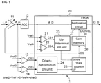
FIG. 1 is a block diagram showing a configuration of an A/D conversion device 1, which is a first embodiment of the present invention. Thedevice 1 includes anamplifier 11, anADC 12,analog comparators device 1 receives an analog signal I_A (first analog signal) as an audio signal, converts the analog signal I_A to a digital signal O_D, and outputs the digital signal O_D to a signal processing device (e.g., a signal processing unit shown inFIG. 3 ) that performs signal processing on the digital signal O_D. - The
amplifier 11 is a variable-gain amplifier that amplifies the analog signal I_A input to the A/D conversion device 1 with a gain corresponding to a current state GS and outputs the amplified analog signal M A (second analog signal). Here, the state GS indicates a stage of the gain of theamplifier 11 specified by theFPGA 20, and in the present embodiment, the gain increases as the state GS increases. - The
ADC 12 is a converter that converts the analog signal M_A to a digital signal M_D (first digital signal). - Vref2 and Vref3 of a first level are respectively given to the
analog comparators amplifier 11, and Vref2 is a reference level on the plus side and Vref3 is a reference level on the minus side. If the voltage of the signal M_A is higher than Vref2, theanalog comparator 13 outputs an H level as a signal CS2, but otherwise theanalog comparator 13 outputs an L level as the signal CS2. If the voltage of the signal M_A is lower than Vref3, theanalog comparator 14 outputs an H level as a signal CS3, but otherwise theanalog comparator 14 outputs an L level as the signal CS3. - As shown in
FIG. 1 , theFPGA 20 is programmed to function asdigital comparators determination unit 23, a down-determination unit 24, astate counter 25, again memory 26, and arestoration circuit 27. - The
state counter 25 is an up-down counter in which the current state GS is stored and that raises the state GS by one in response to an up instruction and immediately lowers the state GS by one in response to a down instruction. An operation for increasing the gain may be delayed from the up instruction to a certain extent. The state GS stored in thestate counter 25 is supplied to theamplifier 11 described above and is used to control the gain. - Vref1 and Vref4 of a second level are respectively given to the
digital comparators amplifier 11. When it is assumed that the analog signal M_A and the digital signal M_D obtained by converting the analog signal M_A are at the same level, there is a relationship Vref2>Vref1>0>Vref4>Vref3 between the levels Vref1 and Vref4 and the levels Vref2 and Vref3 described above. That is, an absolute value of the second level is smaller than an absolute value of the first level. - If the value of the signal M_D is smaller than Vref1, the
digital comparator 21 outputs an H level as a signal CS1, but otherwise thedigital comparator 21 outputs an L level as the signal CS1. Also, if the value of the signal M_D is larger than Vref4, thedigital comparator 22 outputs an H level as a signal CS4, but otherwise thedigital comparator 22 outputs an L level as the signal CS4. - If both of the signals CS1 and CS4 have continuously stayed at the H level for a predetermined period, i.e., if the level of the signal M_D has been continuously kept between Vref1 and Vref4 for the predetermined period, the up-
determination unit 23 transmits an up instruction to thestate counter 25 to raise the state GS by one. - The
digital comparators determination unit 23 constitute an up circuit that detects that the value of the first digital signal M_D has been continuously within the range of the second level from Vref4 to Vref1 for the predetermined period and causes thestate counter 25 to make the state GS transition to a state of gain of the next higher stage. That is, the up circuit switches the gain AG of theamplifier 11 to a gain of the next higher stage if positive and negative peak values of a received audio signal continuously do not reach positive and negative reference values (positive: Vref1/AG(GS), negative: Vref4/AG(GS)) specified with the current state GS, respectively. However, the maximum value of the state GS in thestate counter 25 is 7, and the state GS cannot be raised to a state above 7. - If either the signal CS2 or the signal CS3 reaches the H level, the down-
determination unit 24 transmits a down instruction to thestate counter 25 to lower the state GS by one. The down-determination unit 24 and theanalog comparators state counter 25 to make the state GS transition to a state of gain of the next lower stage. The down-determination unit 24 is a low-delay digital circuit that immediately changes the state GS according to outputs from theanalog comparators amplifier 11 to a gain of the next lower stage at the moment at which either a positive peak value or a negative peak value of a received audio signal moves out of the range between positive and negative reference values (positive: Vref2/AG(GS), negative: Vref3/AG(GS)) specified with the current state GS. However, the minimum value of the state GS in thestate counter 25 is 0, and the state GS cannot be lowered to a state below 0. - The
gain memory 26 is a memory that supplies a gain value DG(GS) that corresponds to the current state GS stored in thestate counter 25 to therestoration circuit 27 at a timing that is delayed by a period of time that corresponds to a signal delay in theADC 12. Therestoration circuit 27 amplifies the digital signal M_D with the gain DG(GS) and outputs the amplified signal as a signal O_D (second digital signal). - Inherently, there are variations in the gain of the
amplifier 11 in each state specified with the state GS due to variations in analog elements such as a resistor. In the present embodiment, measures are taken in thegain memory 26 to correct a gain error that occurs in the signal O_D due to an error between a design value of the gain of theamplifier 11 and an actual gain. - Here, assume that an error ΔG occurs between a design value G of the gain of the
amplifier 11 corresponding to a state and an actual analog gain of theamplifier 11, and the analog gain is G+ΔG. In this case, if digital amplification is performed on the signal M_D in therestoration circuit 27 with again 1/G without the error being taken into consideration, a total gain O_D/I_A is (G+ΔG)/G. The error ΔG differs between amplifiers and states, and may be a positive value or a negative value. Therefore, the total gain varies every time the state is switched, and noise that distorts the signal O_D in a stepwise manner occurs at a point in time at which the state is switched. Therefore, in the present embodiment, when the A/D conversion device 1 is manufactured, the manufacturer measures analog gains AG(GS) of theamplifier 11 for respective states GS, calculates gains DG(GS) for the respective states GS based on the analog gains, and writes a gain table that includes the gains DG(GS) for the plurality of states GS into thegain memory 26. -
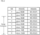
FIG. 2 is a diagram showing the gain table. As shown inFIG. 2 , a gain DG(GS)=BG-AG(GS) of therestoration circuit 27 for each state GS, which is calculated from a measured analog gain AG(GS), is stored in the gain table. Here, BG represents a base gain, and the manufacturer can determine a gain suitable for signal processing that is to be performed at a following stage as the base gain. InFIG. 2 , analog gains AG(GS) are shown as "about 60 dB" and the like because there are variations in the analog gains of theamplifier 11 as described above. - In the example shown in
FIG. 2 , the gains AG(GS) are set at intervals of 10 dB, but this is merely an example of design. Gains AG(GS) may also be set at other intervals or intervals may also be changed at an intermediate stage. - Also, in the example shown in
FIG. 2 , the gain AG(GS) increases as the value of the state GS increases, but, conversely, the gain AG(GS) may also decrease as the value of the state GS increases. In this case, the up instruction and the down instruction are interchanged inFIG. 1 . - Also, a variation range of the state GS (range from GS=0 to GS=5 in the example shown in
FIG. 2 ) may be limited according to an instruction from a user or due to a setting. For example, if it is known that a signal (a signal of a line level) for which high gain is not needed will be input to the A/D conversion device 1, unnecessary gain switching can be reduced by setting an upper limit of the variation range of the state GS. Details of this limitation will be described later in relation toFIG. 6 . - When the gain of the
amplifier 11 is switched, transient noise occurs in addition to noise due to an error of the analog gain of theamplifier 11. Therefore, in the present embodiment, when the state GS is switched, thegain memory 26 transmits a signal gc that indicates the timing of the switching to therestoration circuit 27. Therestoration circuit 27 amplifies the signal M_D with the gain DG(GS) and performs calculation to reduce transient noise included in the amplified signal M_D' at a timing corresponding to the signal gc. Therestoration circuit 27 obtains a signal O_D that is to be output from thedevice 1 by replacing, with an interpolation sample, a sample of the amplified signal M_D' within a period during which the transient noise due to switching of the gain appears in the signal M_D, more specifically, within a predetermined period from the output timing of the signal gc. The interpolation sample is calculated based on the signal M_D' before and after the period. Thus, it is possible to reduce the transient noise that occurs in the signal O_D due to switching of the gain of theamplifier 11. The transient noise can be reduced using not only such a replacement method but also a noise reduction filter according to characteristics of the transient noise. For example, a configuration is also possible in which, out of a series of samples of the signal M_D', a sample of the transient noise within a period during which the transient noise is included is predicted based on samples before the period, and the predicted noise is removed. - Next, operations and effects of the present embodiment will be described. In the present embodiment, comparison with the first level for determining to reduce the gain of the
amplifier 11, which needs to be performed at high speed, is performed using the second analog signal M_A before A/D conversion. If the audio signal exceeds the range defined by the first level, a determination to reduce the gain can be made at high speed to prevent clipping of the audio signal in theADC 12. - On the other hand, comparison with the second level for determining to increase the gain of the
amplifier 11, which need not be performed at high speed, is performed through digital comparison using the signal M_D after A/D conversion. The digital comparison is realized using only a portion of a digital processing circuit such as an existing FPGA. On the other hand, analog comparators and an analog circuit that generates the second level are omitted from the A/D conversion device 1, and therefore the cost and power consumption of the entire device can be reduced. - Also, in the present embodiment, the state GS is caused to transition to the state of gain of the next higher stage when it is detected that the audio signal (signal M_D) has been continuously within the range of the second level for the predetermined period. The gain of the
amplifier 11 is not increased even if the audio signal (signal M_D) is small for a short period, and frequent switching of the gain can be prevented. - Also, according to the present embodiment, a plurality of gains DG(GS) that correspond to measurement values of the gain of the
amplifier 11 in a plurality of states are stored in thegain memory 26. Also, therestoration circuit 27 amplifies the signal M_D with a gain DG(GS) that is stored in thegain memory 26 and corresponds to the current state GS, and outputs the amplified signal as the signal O_D. Therefore, even if the state is switched in the A/D conversion device 1, the gain of the audio signal (i.e., signal O_D/signal I_A) in theentire device 1 does not vary. - Also, in the present embodiment, the
restoration circuit 27 reduces the transient noise in a series of samples of the signal M_D amplified with the gain DG(GS), and therefore the output signal O_D includes almost no transient noise even if the gain of theamplifier 11 is switched. -
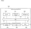
FIG. 3 is a block diagram showing an example configuration of anaudio processing device 100 that includes the same A/D conversion device as that described above. Theaudio processing device 100 is, for example, a digital mixer, a signal processing engine, an audio device, an electronic musical instrument, an effector, a PC, a smartphone, or a tablet terminal. Theaudio processing device 100 may be any device that receives an analog audio signal, converts the analog signal to a digital signal, and processes the digital signal. - As shown in
FIG. 3 , theaudio processing device 100 includes acontrol unit 110, a UI (User Interface)unit 120, astorage unit 130, an A/D conversion device 140, asignal processing unit 150, a DAC (Digital Analog Converter) 160, and abus 170 that connects these elements to each other. - The
control unit 110 is a control circuit that controls the entireaudio processing device 100 and is constituted by one or more CPUs, for example. TheUI unit 120 includes an operation unit that supplies information regarding an operation made by a user to thecontrol unit 110 in response to the operation and a display unit that visually provides information from thecontrol unit 110 to the user, for example. Thestorage unit 130 stores programs that are executed by thecontrol unit 110, control information that is used by thecontrol unit 110, and the like. The A/D conversion device 140 is the same circuit as thedevice 1 shown inFIG. 1 and converts an analog audio signal I_A to a digital audio signal O_D. Thesignal processing unit 150 performs signal processing according to an instruction from thecontrol unit 110 on the audio signal O_D output from the A/D conversion device 140 and outputs the processed audio signal to theDAC 160. TheDAC 160 converts the digital audio signal output from thesignal processing unit 150 to an analog audio signal and outputs the analog signal to a sound emission device such as a powered speaker on the outside of theaudio processing device 100. - The A/
D conversion device 140 of this application example includes four registers R1 to R4 (not shown) in which values of the reference levels Vref1 to Vref4 are stored and a register UL (not shown) in which an upper limit value of the variation range of the state GS is stored. Setting values of the registers R1 and R4 are supplied as Vref1 and Vref4 to thedigital comparators FIG. 1 . Setting values of the registers R2 and R3 are converted to analog voltages Vref2 and Vref3 by a D/A converter (not shown) and are supplied to theanalog comparators device 1. -
FIGS. 4 to 6 are flowcharts showing processing contents of a program that is executed by thecontrol unit 110 in this application example. When the power source of theaudio processing device 100 is turned ON, thecontrol unit 110 reads a main routine shown in the flowchart ofFIG. 4 from thestorage unit 130 and executes the routine. - First, the
control unit 110 executes initial setting (step S101). In the initial setting, thecontrol unit 110 reads a program that is to be caused to function as the FPGA20 shown inFIG. 2 from thestorage unit 130 and writes the program into an FPGA of the A/D conversion device 140. - Next, the
control unit 110 detects various events that occur in the audio processing device 100 (step S102) and determines the presence or absence of these events (step S103). - If it is determined in step S103 that no event has occurred, the
control unit 110 repeats detection of the events (step S102) and determination of the presence or absence of the events (step S103). - On the other hand, if it is determined in step S103 that an event has occurred, the
control unit 110 executes event processing corresponding to the detected event (step S104), and thereafter repeats detection of the events (step S102) and determination of the presence or absence of the events (step S103). -
FIG. 5 is a flowchart of event processing that is executed in step S104 upon detection of an operation event indicating that the user has made an operation to change the value of any one of the reference levels Vref1 to Vref4. In this event processing, out of the registers R1 to R4, a register that corresponds to the specified reference level is set to a value that corresponds to the operation. Thus, out of Vref1 to Vref4 shown inFIG. 1 , a reference level that corresponds to the set register is changed to a level that corresponds to the set value. -
FIG. 6 is a flowchart of event processing that is executed in step S104 upon detection of an operation event indicating that the user has made an operation to set the variation range of the state GS. In this event processing, an upper limit (5 in the example shown inFIG. 2 ) of the variation range of the state that the user specified by operating theUI unit 120 is set in the register UL in the A/D conversion device 140. When the register UL is set, the upper limit value indicated by the register UL serves as the maximum value of the state GS in thestate counter 25. If the current state GS reaches the upper limit value indicated by the UL, thestate counter 25 does not raise the state GS even when an up instruction is received. - In the A/D conversion device of the first embodiment, the
FPGA 20 functions as the up circuit, but the up circuit need not operate at high speed, and therefore thecontrol unit 110 shown inFIG. 3 functions as the up circuit in the second embodiment. - The configuration of the A/D conversion device in the second embodiment is essentially the same as that shown in
FIG. 2 , but theFPGA 20 does not include the up circuit (thecomparators control unit 110 functions as the up circuit by reading a program shown inFIG. 7 from thestorage unit 130 and executing the program. Also, the registers R1, R4, and UL can be omitted from the A/D conversion device, and the A/D conversion device includes the registers R2 and R3, registers Rmax and Rmin for giving the maximum value and the minimum value of the signal M_D to thecontrol unit 110, and a register S for receiving an up signal from thecontrol unit 110. -
FIG. 7 is a flowchart of interruption processing that is executed in step S104 upon detection of an interruption event of a timer that periodically occurs. In this interruption processing, thecontrol unit 110 first acquires a max value and a min value of the signal M_D that occurred between previous interruption processing and current interruption processing from the registers Rmax and Rmin in the A/D conversion device 140 (step S401). - Next, the
control unit 110 determines whether or not the reference level Vref1 is larger than the max value (step S402), and if the result of determination is "NO", ends the event processing routine. If the result of determination performed in step S402 is "YES", thecontrol unit 110 determines whether or not the min value is larger than the reference level Vref4, and if the result of determination is "NO", ends the event processing routine. If the result of determination performed in step S403 is "YES", thecontrol unit 110 determines whether or not results of determination performed in steps S402 and S403 have been continuously "YES" for a predetermined period, and if the result of determination is "NO", ends the event processing routine. It is possible to provide a measurement counter and measure the duration for which the results are "YES" as a count value of the counter, for example. More specifically, if the result of determination performed in step S403 is "YES" in both of the previous interruption processing and the current interruption processing, the counter is incremented, and if the result is "NO" in the previous interruption processing and "YES" in the current interruption processing, the counter is reset to 1. In this case, the duration is measured as a count value of the measurement counter. Accordingly, when the count value has reached a predetermined value, it can be determined that results of determination performed in steps S402 and S403 have been continuously "YES" for the predetermined period. - If the result of determination performed in step S404 is "YES", i.e., if the signal M_D has stayed at a level between Vref4 and Vref1 for the predetermined period, the
control unit 110 writes an up instruction into the register S (step S405), and ends the event processing routine. In response to the up instruction to the register S, thestate counter 25 of the A/D conversion device changes the state GS to a state of gain of the next higher stage. However, if a down instruction is given from the down circuit during a period from when the max value and the min value are read in step S401 to when the up instruction is given in step S405, thestate counter 25 ignores the up instruction and does not change the state GS. - As described above, in the present embodiment, the functions of the
digital comparators determination unit 23 in the above-described first embodiment are realized as a result of thecontrol unit 110 executing the program. - Effects similar to those achieved in the above-described first embodiment are also achieved in the present embodiment. Also, in the present embodiment, the
control unit 110 performs up determination, and therefore there is an advantage in that it is easy to dynamically change conditions for the up determination such as the reference levels and the predetermined period. - Although the first embodiment and the second embodiment of the present invention have been described, other embodiments of the present invention are also possible. The following are examples.
- (1) Out of the four reference levels, Vref2 and Vref3 may be set to levels that have the same absolute value and opposite polarities. Likewise, Vref1 and Vref4 may be set to levels that have the same absolute value and opposite polarities. Thus, the four registers R1 to R4 can be reduced to two registers (e.g., R1 and R2).
- (2) In the above-described first embodiment, control for reducing the gain by a single state is performed based on comparison between the signal M_A and the first level, but, instead of the signal M A, a signal that is obtained by performing full wave rectification on the signal M_A may be compared with the first level. Also, in the above-described first embodiment, control for increasing the gain by a single state is performed based on comparison between the signal M_D and the second level, but, instead of the signal M_D, a signal that is obtained by performing full wave rectification on the signal M_D may be compared with the second level. In these cases, it is possible to halve the number of analog comparators used in the former comparison and the number of digital comparators used in the latter comparison, but a response time on the negative side becomes longer than a response time on the positive side in the analog comparator.
-
1, 140 A/ D conversion device 11 Amplifier 12 ADC 13, 14 Analog comparator 20 FPGA 1,22 Digital comparator 23 Up- determination unit 24 Down- determination unit 25 State counter 26 Gain memory 27 Restoration circuit 100 Audio processing device 110 Control unit 120 UI unit 130 Storage unit 140 A/ D conversion device 150 Signal processing unit 160 DAC 170 Bus
Claims (9)
- An A/D conversion device comprising:an amplifier configured to perform analog amplification on a first analog signal with a gain corresponding to a state and output the amplified signal as a second analog signal;a converter configured to convert the second analog signal to a digital signal and output the digital signal as a first digital signal;a down circuit configured to detect that the second analog signal exceeds a range defined by a first level and cause the state to transition to a state of gain of the next lower stage; andan up circuit configured to detect that the first digital signal has been continuously within a range defined by a second level for a predetermined period and cause the state to transition to a state of gain of the next higher stage, an absolute value of the second level being smaller than an absolute value of the first level.
- The A/D conversion device according to claim 1, wherein
the down circuit includes an analog comparator that compares the second analog signal with the first level. - The A/D conversion device according to claim 2, wherein
the down circuit further includes a low-delay digital circuit that changes the state according to an output from the analog comparator. - The A/D conversion device according to any one of claims 1 to 3, further comprising
a restoration circuit that performs digital amplification on the first digital signal with a gain corresponding to the gain of the amplifier and outputs the amplified signal as a second digital signal. - The A/D conversion device according to claim 4, further comprisinga memory in which a gain value that corresponds to an analog gain of the amplifier is stored for each state, andthe restoration circuit amplifies the first digital signal with a gain corresponding to a gain value that is stored in the memory and corresponds to the state, and outputs the amplified signal as the second digital signal.
- The A/D conversion device according to claim 4 or 5, wherein
the restoration circuit reduces influence of transient noise in the first digital signal on the second digital signal, the transient noise occurring at a timing of transition of the state. - The A/D conversion device according to claim 6, wherein
the restoration circuit reduces the influence of the noise on the second digital signal by replacing, out of a series of samples of the first digital signal, a sample in which the transient noise is included with an interpolation sample. - The A/D conversion device according to claim 6, wherein
the restoration circuit reduces the transient noise using a noise reduction filter. - A method for controlling an A/D conversion device that includes an amplifier that performs analog amplification on a first analog signal with a gain corresponding to a state and outputs the amplified signal as a second analog signal and a converter that converts the second analog signal to a digital signal and outputs the digital signal as a first digital signal, the method comprising:upon detecting that the second analog signal exceeds a range defined by a first level, immediately causing the state to transition to a state of gain of the next lower stage; andupon detecting that the first digital signal has been continuously within a range defined by a second level for a predetermined period, causing the state to transition to a state of gain of the next higher stage, an absolute value of the second level being smaller than an absolute value of the first level.
Applications Claiming Priority (2)
| Application Number | Priority Date | Filing Date | Title |
|---|---|---|---|
| JP2019052618A JP7218637B2 (en) | 2019-03-20 | 2019-03-20 | A/D conversion device and A/D conversion method |
| PCT/JP2020/005453 WO2020189106A1 (en) | 2019-03-20 | 2020-02-13 | A/d conversion device and a/d conversion method |
Publications (2)
| Publication Number | Publication Date |
|---|---|
| EP3944504A1 true EP3944504A1 (en) | 2022-01-26 |
| EP3944504A4 EP3944504A4 (en) | 2022-12-21 |
Family
ID=72520686
Family Applications (1)
| Application Number | Title | Priority Date | Filing Date |
|---|---|---|---|
| EP20773718.0A Withdrawn EP3944504A4 (en) | 2019-03-20 | 2020-02-13 | A/d conversion device and a/d conversion method |
Country Status (5)
| Country | Link |
|---|---|
| US (1) | US11894858B2 (en) |
| EP (1) | EP3944504A4 (en) |
| JP (1) | JP7218637B2 (en) |
| CN (1) | CN113574804B (en) |
| WO (1) | WO2020189106A1 (en) |
Families Citing this family (2)
| Publication number | Priority date | Publication date | Assignee | Title |
|---|---|---|---|---|
| US12199626B2 (en) * | 2021-11-01 | 2025-01-14 | Electronics And Telecommunications Research Institute | Dynamic high-resolution analog to digital converter and operating method thereof |
| JP2024064359A (en) * | 2022-10-28 | 2024-05-14 | 株式会社小野測器 | Sensor signal converter |
Family Cites Families (18)
| Publication number | Priority date | Publication date | Assignee | Title |
|---|---|---|---|---|
| JPS6465927A (en) * | 1987-09-04 | 1989-03-13 | Fujitsu Ltd | Automatic gain switching system for a/d converter |
| JP3183417B2 (en) * | 1992-04-17 | 2001-07-09 | ソニー株式会社 | A / D converter |
| JPH05343994A (en) * | 1992-06-05 | 1993-12-24 | Fujitsu Ltd | Analog signal level conversion circuit |
| JPH06260861A (en) * | 1993-03-02 | 1994-09-16 | Hitachi Denshi Ltd | Demodulator |
| JPH09130245A (en) | 1995-11-06 | 1997-05-16 | Sony Corp | Variable gain circuit |
| KR100360415B1 (en) * | 2001-02-28 | 2002-11-13 | 삼성전자 주식회사 | Clamp circuit and method for having wide dynamic range of input image signal and minimizing line noise |
| US7218258B2 (en) * | 2004-02-05 | 2007-05-15 | Broadcom Corporation | Method and system for mixed analog-digital automatic gain control |
| US7468760B2 (en) * | 2005-03-31 | 2008-12-23 | Mstar Semiconductor, Inc. | Apparatus and related method for level clamping control |
| US7408493B2 (en) * | 2005-05-20 | 2008-08-05 | Texas Instruments Incorporated | Systems and methods for automatic gain control |
| JP4628881B2 (en) * | 2005-06-15 | 2011-02-09 | ルネサスエレクトロニクス株式会社 | Variable gain amplifier circuit, DC offset correction method thereof, and wireless receiver |
| CN101400994B (en) * | 2005-10-14 | 2013-03-27 | 奥林巴斯Ndt公司 | Digital time variable gain circuit for non-destructive test instrument |
| TWI311893B (en) * | 2006-09-13 | 2009-07-01 | Coretronic Corporatio | Audio control method and acoustic processing system |
| CN101557205B (en) * | 2009-05-26 | 2011-04-06 | 中国科学院微电子研究所 | A Mixed Mode AGC Loop |
| WO2011074193A1 (en) * | 2009-12-15 | 2011-06-23 | パナソニック株式会社 | Automatic gain control device and electronic apparatus |
| EP2485395B1 (en) | 2011-02-04 | 2013-05-01 | Harman International Industries Ltd. | Audio Mixing Console avoiding Signal Level Overload |
| JP2015115680A (en) * | 2013-12-10 | 2015-06-22 | ソニー株式会社 | Signal processing device, signal processing method, and program |
| GB2533300B (en) * | 2014-12-15 | 2017-03-22 | Nordic Semiconductor Asa | Packet-based radio receiver with automatic gain control |
| JP6786829B2 (en) | 2016-03-18 | 2020-11-18 | ヤマハ株式会社 | AD converter |
-
2019
- 2019-03-20 JP JP2019052618A patent/JP7218637B2/en active Active
-
2020
- 2020-02-13 CN CN202080021073.2A patent/CN113574804B/en active Active
- 2020-02-13 WO PCT/JP2020/005453 patent/WO2020189106A1/en not_active Ceased
- 2020-02-13 EP EP20773718.0A patent/EP3944504A4/en not_active Withdrawn
-
2021
- 2021-09-17 US US17/477,712 patent/US11894858B2/en active Active
Also Published As
| Publication number | Publication date |
|---|---|
| JP7218637B2 (en) | 2023-02-07 |
| CN113574804A (en) | 2021-10-29 |
| EP3944504A4 (en) | 2022-12-21 |
| CN113574804B (en) | 2025-07-04 |
| JP2020155931A (en) | 2020-09-24 |
| US11894858B2 (en) | 2024-02-06 |
| WO2020189106A1 (en) | 2020-09-24 |
| US20220006468A1 (en) | 2022-01-06 |
Similar Documents
| Publication | Publication Date | Title |
|---|---|---|
| US7965208B2 (en) | Auto ranging system and method for analog signal | |
| US11894858B2 (en) | A/D conversion device and A/D conversion method | |
| CN106324333A (en) | High-precision voltage measuring device | |
| JPH0856160A (en) | Abnormality detector for a/d converter | |
| WO2019176332A1 (en) | Sensor device | |
| US20050030099A1 (en) | AGC circuit | |
| US11451238B2 (en) | Recording device and recording method | |
| CN116937947A (en) | Method and system for switching self-adaptive circuit based on current range | |
| JP2017083249A (en) | Pulse height analyzer | |
| JPH07273650A (en) | A/d converter circuit for nonlinear signal | |
| US11509322B2 (en) | Light sensor circuit | |
| JP4647284B2 (en) | Analog / digital conversion method and analog / digital conversion circuit | |
| JP2005214849A (en) | Automatic gain control circuit | |
| JP2010068572A (en) | Digital potentiometer and protective relay | |
| CN110933319B (en) | Image signal sampling processing method and circuit | |
| KR100417114B1 (en) | Apparatus and method to measure high frequency power | |
| JP2599503Y2 (en) | Sensor device | |
| KR20040084087A (en) | Analog input module of programmable logic controller | |
| KR20000056025A (en) | Analog input circuit for plc system and control method thereof | |
| JP7553042B2 (en) | Signal processing circuit and load detection device | |
| CN120214395A (en) | Amplification factor adjustment method for current detection and current detector | |
| CN114553160A (en) | Automatic gain control method, controller and amplifying circuit | |
| JPH08128851A (en) | Sensor output signal-processing circuit | |
| KR20070105195A (en) | temperature Senser | |
| KR19980083129A (en) | Input / output value monitoring method of analog / digital converter |
Legal Events
| Date | Code | Title | Description |
|---|---|---|---|
| STAA | Information on the status of an ep patent application or granted ep patent |
Free format text: STATUS: THE INTERNATIONAL PUBLICATION HAS BEEN MADE |
|
| PUAI | Public reference made under article 153(3) epc to a published international application that has entered the european phase |
Free format text: ORIGINAL CODE: 0009012 |
|
| STAA | Information on the status of an ep patent application or granted ep patent |
Free format text: STATUS: REQUEST FOR EXAMINATION WAS MADE |
|
| 17P | Request for examination filed |
Effective date: 20210930 |
|
| AK | Designated contracting states |
Kind code of ref document: A1 Designated state(s): AL AT BE BG CH CY CZ DE DK EE ES FI FR GB GR HR HU IE IS IT LI LT LU LV MC MK MT NL NO PL PT RO RS SE SI SK SM TR |
|
| DAV | Request for validation of the european patent (deleted) | ||
| DAX | Request for extension of the european patent (deleted) | ||
| REG | Reference to a national code |
Ref country code: DE Ref legal event code: R079 Free format text: PREVIOUS MAIN CLASS: H03M0001120000 Ipc: H03G0003300000 |
|
| A4 | Supplementary search report drawn up and despatched |
Effective date: 20221117 |
|
| RIC1 | Information provided on ipc code assigned before grant |
Ipc: H03M 1/12 20060101ALN20221111BHEP Ipc: H03M 1/18 20060101ALI20221111BHEP Ipc: H03G 3/30 20060101AFI20221111BHEP |
|
| STAA | Information on the status of an ep patent application or granted ep patent |
Free format text: STATUS: THE APPLICATION IS DEEMED TO BE WITHDRAWN |
|
| 18D | Application deemed to be withdrawn |
Effective date: 20230617 |