EP3937267A1 - Graphene-containing film, production method thereof, graphene-containing film laminate, and photoelectric conversion element - Google Patents
Graphene-containing film, production method thereof, graphene-containing film laminate, and photoelectric conversion element Download PDFInfo
- Publication number
- EP3937267A1 EP3937267A1 EP19915584.7A EP19915584A EP3937267A1 EP 3937267 A1 EP3937267 A1 EP 3937267A1 EP 19915584 A EP19915584 A EP 19915584A EP 3937267 A1 EP3937267 A1 EP 3937267A1
- Authority
- EP
- European Patent Office
- Prior art keywords
- graphene
- membrane
- photoelectric conversion
- containing membrane
- anode
- Prior art date
- Legal status (The legal status is an assumption and is not a legal conclusion. Google has not performed a legal analysis and makes no representation as to the accuracy of the status listed.)
- Granted
Links
Images



Classifications
-
- H—ELECTRICITY
- H10—SEMICONDUCTOR DEVICES; ELECTRIC SOLID-STATE DEVICES NOT OTHERWISE PROVIDED FOR
- H10F—INORGANIC SEMICONDUCTOR DEVICES SENSITIVE TO INFRARED RADIATION, LIGHT, ELECTROMAGNETIC RADIATION OF SHORTER WAVELENGTH OR CORPUSCULAR RADIATION
- H10F77/00—Constructional details of devices covered by this subclass
- H10F77/20—Electrodes
- H10F77/244—Electrodes made of transparent conductive layers, e.g. transparent conductive oxide [TCO] layers
-
- H—ELECTRICITY
- H05—ELECTRIC TECHNIQUES NOT OTHERWISE PROVIDED FOR
- H05B—ELECTRIC HEATING; ELECTRIC LIGHT SOURCES NOT OTHERWISE PROVIDED FOR; CIRCUIT ARRANGEMENTS FOR ELECTRIC LIGHT SOURCES, IN GENERAL
- H05B33/00—Electroluminescent light sources
- H05B33/12—Light sources with substantially two-dimensional [2D] radiating surfaces
- H05B33/26—Light sources with substantially two-dimensional [2D] radiating surfaces characterised by the composition or arrangement of the conductive material used as an electrode
- H05B33/28—Light sources with substantially two-dimensional [2D] radiating surfaces characterised by the composition or arrangement of the conductive material used as an electrode of translucent electrodes
-
- H—ELECTRICITY
- H10—SEMICONDUCTOR DEVICES; ELECTRIC SOLID-STATE DEVICES NOT OTHERWISE PROVIDED FOR
- H10F—INORGANIC SEMICONDUCTOR DEVICES SENSITIVE TO INFRARED RADIATION, LIGHT, ELECTROMAGNETIC RADIATION OF SHORTER WAVELENGTH OR CORPUSCULAR RADIATION
- H10F71/00—Manufacture or treatment of devices covered by this subclass
- H10F71/138—Manufacture of transparent electrodes, e.g. transparent conductive oxides [TCO] or indium tin oxide [ITO] electrodes
-
- H—ELECTRICITY
- H10—SEMICONDUCTOR DEVICES; ELECTRIC SOLID-STATE DEVICES NOT OTHERWISE PROVIDED FOR
- H10F—INORGANIC SEMICONDUCTOR DEVICES SENSITIVE TO INFRARED RADIATION, LIGHT, ELECTROMAGNETIC RADIATION OF SHORTER WAVELENGTH OR CORPUSCULAR RADIATION
- H10F77/00—Constructional details of devices covered by this subclass
- H10F77/10—Semiconductor bodies
- H10F77/12—Active materials
-
- H—ELECTRICITY
- H10—SEMICONDUCTOR DEVICES; ELECTRIC SOLID-STATE DEVICES NOT OTHERWISE PROVIDED FOR
- H10F—INORGANIC SEMICONDUCTOR DEVICES SENSITIVE TO INFRARED RADIATION, LIGHT, ELECTROMAGNETIC RADIATION OF SHORTER WAVELENGTH OR CORPUSCULAR RADIATION
- H10F77/00—Constructional details of devices covered by this subclass
- H10F77/20—Electrodes
- H10F77/244—Electrodes made of transparent conductive layers, e.g. transparent conductive oxide [TCO] layers
- H10F77/247—Electrodes made of transparent conductive layers, e.g. transparent conductive oxide [TCO] layers comprising indium tin oxide [ITO]
-
- H—ELECTRICITY
- H10—SEMICONDUCTOR DEVICES; ELECTRIC SOLID-STATE DEVICES NOT OTHERWISE PROVIDED FOR
- H10K—ORGANIC ELECTRIC SOLID-STATE DEVICES
- H10K30/00—Organic devices sensitive to infrared radiation, light, electromagnetic radiation of shorter wavelength or corpuscular radiation
- H10K30/80—Constructional details
- H10K30/81—Electrodes
- H10K30/82—Transparent electrodes, e.g. indium tin oxide [ITO] electrodes
-
- H—ELECTRICITY
- H10—SEMICONDUCTOR DEVICES; ELECTRIC SOLID-STATE DEVICES NOT OTHERWISE PROVIDED FOR
- H10K—ORGANIC ELECTRIC SOLID-STATE DEVICES
- H10K50/00—Organic light-emitting devices
- H10K50/80—Constructional details
- H10K50/805—Electrodes
- H10K50/82—Cathodes
- H10K50/828—Transparent cathodes, e.g. comprising thin metal layers
-
- H—ELECTRICITY
- H10—SEMICONDUCTOR DEVICES; ELECTRIC SOLID-STATE DEVICES NOT OTHERWISE PROVIDED FOR
- H10K—ORGANIC ELECTRIC SOLID-STATE DEVICES
- H10K85/00—Organic materials used in the body or electrodes of devices covered by this subclass
- H10K85/10—Organic polymers or oligomers
- H10K85/111—Organic polymers or oligomers comprising aromatic, heteroaromatic, or aryl chains, e.g. polyaniline, polyphenylene or polyphenylene vinylene
- H10K85/113—Heteroaromatic compounds comprising sulfur or selene, e.g. polythiophene
- H10K85/1135—Polyethylene dioxythiophene [PEDOT]; Derivatives thereof
Definitions
- Embodiments of the present disclosure relate to a graphene-containing membrane, a process for producing the membrane, a graphene-containing membrane laminate, and a photoelectric conversion device.
- ITO films are normally formed by sputtering or the like. In order that the ITO films can have high electroconductivity, it is necessary to carry out the sputtering procedure at a high temperature and to anneal thereafter the formed films at a high temperature. However, it is often the case that organic materials cannot be subjected to those procedures at a high temperature. Further, when the ITO films are installed in the devices, metal ions such as indium ion and/or halogen ions may intrude into the active elements such as the photoelectric conversion layers to impair the activity of the devices.
- TCO transparent conductive oxide
- Ag or an alloy thereof
- silver nanowires are adopted as the transparent electrodes.
- silver is often deteriorated by acids or halogens.
- silver tends to cause migration and, as a result, may react with water and the like to lower the transparency of the electrode or may migrate into the active elements to impair the activity of the devices.
- metal ions contained in TCO may diffuse to impair the device activity.
- graphene-containing membranes are adopted as the material of transparent electrode.
- graphene-containing membranes are known to have various disadvantages. Specifically, there are many restrictions on their processing. For example, they need to be produced by CVD and the formed graphene membranes must be treated with hydrazine vapor.
- Graphene membranes can be also formed by wet-coating, but the resultant graphene-containing membranes often have poor electrical properties and hence photoelectric conversion devices comprising them may have unsatisfying performances.
- Patent document 1 Japanese Patent Laid-Open No. H12-089786
- the present embodiment provides a graphene-containing membrane which can be prepared by coating method and has excellent electrical properties, a producing process thereof, graphene-containing membrane laminate, and photoelectric conversion device.
- a graphene-containing membrane according to the first embodiment contains graphene in which polyethyleneimine chains are connected to the graphene skeleton, which has a ratio of the photoelectron intensity at the energy peak position of C1s orbital to that at the bonding energy on an X-ray photoelectron spectrum measured on an ITO film of 288 eV in a range of 5.5 to 20.
- a graphene-containing membrane producing process according to the second embodiment comprises, in this order, the steps of:
- a graphene-containing membrane laminate according to the third embodiment has a structure comprising a graphene oxide film overlaid on a membrane containing graphene combined with polyethyleneimine chains.
- a photoelectric conversion device comprises an anode, a cathode, a photoelectric conversion layer provided between said anode and said cathode, and a graphene-containing membrane provided between said cathode and said photoelectric conversion layer; wherein said graphene-containing membrane contains graphene in which polyethyleneimine chains are connected to the graphene skeleton and has a ratio of the photoelectron intensity at the energy peak position of C1s orbital to that at the bonding energy on an X-ray photoelectron spectrum measured on an ITO film of 288 eV in a range of 5.5 to 20.
- a photoelectric conversion device comprises an anode, a cathode, a photoelectric conversion layer provided between said anode and said cathode, and such a laminate provided between said anode and said photoelectric conversion layer as has a structure comprising a graphene oxide film overlaid on a membrane containing graphene to which polyethyleneimine chains are connected from the anode side.
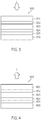
- a graphene-containing membrane 100 has a structure in which one to several layers of graphene 101 are piled up.
- the graphene-containing membrane of the embodiment has a structure in which one to several layers of sheet-shaped graphene 101 are piled up.
- the number of the piled graphene layers is preferably one to six, more preferably two to four so as to obtain sufficient transparency, electroconductivity and ion shielding effect.
- the above graphene has a structure comprising a graphene skeleton to which polyalkyleneimine chains, for example, represented by the following formula, particularly polyethyleneimine chains are connected.
- polyalkyleneimine chains for example, represented by the following formula, particularly polyethyleneimine chains are connected.
- carbon atoms in the graphene skeleton are partly replaced with nitrogen atoms.
- polyethyleneimine chains are shown as an example of the polyalkyleneimine chains.
- n is preferably 2 to 8.
- the graphene shown above can be considered to have a graphene skeleton whose surface is modified with polyalkyleneimine chains.
- Figure 1 schematically shows graphene skeletons 102 having surfaces modified with polyalkyleneimine chains 103.
- the graphene-containing membrane exhibits a characteristic X-ray photoelectron spectrum (i.e., XPS spectrum). Specifically, when measured on an ITO film, the graphene-containing membrane shows an X-ray photoelectron spectrum in which a ratio of the photoelectron intensity at the energy peak position of C1s orbital (I C1s ) to that at the bonding energy of 288 eV (I 288 ), namely, a ratio of I C1s /I 288 (hereinafter, referred to as "R C1s ”) is in a range of 5.5 to 20, preferably 6 to 10.
- the energy peak position of C1s orbital may shift depending on the kind of substituents contained in the graphene-containing membrane, on the content thereof and on the kind of the substrate, but is generally observed at the bonding energy of about 285 eV.
- graphene combined with polyalkyleneimine chains has relatively high insulating property and hence tends to have high electric resistance.
- the graphene-containing membrane of the embodiment which exhibits the above XPS spectrum, contains C-C bonds (including double bonds) in a high ratio as compared with carbonyl carbons and hence tends to have low electric resistance and small work function.
- Quantera SXM As an XPS (X-ray photoelectron spectroscopy) apparatus employed for evaluation, Quantera SXM ([trademark], manufactured by PHI Inc.) can be adopted, for example.
- This apparatus is equipped with a single crystal-monochromatized AlKa X-ray source, and the X-ray output and X-ray analysis area can be set at 50 W and ⁇ 200 ⁇ m, respectively.
- the pass energy under the measurement condition is set to be 280.0 eV (1.0 eV/step) for wide scan and 69.0 eV (0.125 eV/step) for narrow scan.
- the apparatus is also equipped with a charge neutralization gun using both Ar + and e - .
- signals in the XPS spectrum may slightly sift depending on the kind of the substrate.
- the XPS signals defined in the embodiment are limited to those obtained by measuring the membrane on an ITO film.
- the ITO film it is possible to adopt, for example, a transparent electrode of ITO/silver alloy/ITO having a surface resistance of about 10 ⁇ /square (commercially available from OIKE & Co., Ltd.).
- the graphene-containing membrane of the embodiment When measured on an ITO film, the graphene-containing membrane of the embodiment preferably shows an X-ray photoelectron spectrum indicating the bonding energy of the peak corresponding to N1s orbital (hereinafter, referred to as "E N1s ”) in the range of 399.0 to 399.5 eV. If this condition is satisfied, the membrane tends to contain so many pyridine nitrogen atoms, which are fixed in aromatic rings, that the n-electron system can be expanded enough to lower electric resistance. In addition, if containing many pyridine nitrogen atoms, the membrane tends to have high ability of trapping halogen ions and metal ions.
- the graphene-containing membrane of the embodiment preferably has a work function of 4 eV or less, provided that the work function is determined by ultraviolet photoelectron spectroscopy (UPS). If the graphene membrane satisfying this condition is so installed in a photoelectric conversion device that it may be placed between the anode and the photoelectric conversion layer, the anode tends to be improved in function.
- UPS ultraviolet photoelectron spectroscopy
- the measurement of ultraviolet photoelectron spectroscopy is, for example, carried out with Versa Probe ([trademark], manufactured by PHI Inc.) by use of He I line (21.22 eV) as the light source.
- Versa Probe [trademark], manufactured by PHI Inc.
- He I line 21.22 eV
- the sample stage is exposed to a voltage of -13 V during the measurement.
- a gold reference having a surface beforehand subjected to Ar ion etching (cleaning) is measured.
- a graphene-containing membrane producing process of the embodiment comprises, in this order, the steps of:
- the aqueous dispersion of graphene oxide in the above step (a) can be prepared by dispersing graphene oxide in an aqueous medium.
- the graphene oxide used here contains monolayer graphene oxide sheets in an amount of preferably 80 mass% or more, further preferably 90 mass% or more. If satisfying this condition, the graphene oxide can improve homogeneity of the prepared dispersion and also evenness of the coating film.
- As the aqueous dispersion medium water such as pure water or ion-exchanged water is adopted. Further, the medium may contain a small amount of aqueous organic solvent such as methanol or ethanol, if necessary.
- the content of graphene oxide in the dispersion is preferably 0.01 to 1 mass% based on the total mass of the dispersion.
- the mass ratio between the graphene oxide contained in the aqueous dispersion and the polyalkyleneimine to be added therein is preferably 1:3 to 1:20, more preferably 1:7 to 1:15. If the polyalkyleneimine is added in a small amount, dispersibility in the dispersion tends to be lowered. On the other hand, if containing the polyalkyleneimine in a large amount, the resultant film tends to have large electric resistance.
- the polyalkyleneimine preferably has 2 to 8 carbon atomsr. Examples thereof include polyethyleneimine, polypropyleneimine, and polyethylenepropyleneimine. Among them, polyethyleneimine is preferred. It is also possible to use polyalkyleneimines having various structures, such as, straight chain structure, branched chain structure and cyclic structure. However, polyalkyleneimine of branched chain structure is preferred because it makes easy to improve dispersibility.
- Heating time and temperature are so selected that the polyalkyleneimine can react effectively with the graphene oxide. They can be freely determined according to other conditions, but the mixture is generally heated at 80 to 100°C for 30 to 180 minutes.
- the reducing agent used in the above step (b) is not particularly restricted unless it impairs the effect of the embodiment.
- the agent is hence selected from reductants capable of working effectively in aqueous dispersions.
- Example thereof include hydrazine hydrate and sodium borohydride, and hydrazine hydrate is preferred because it provides an appropriate reaction rate.
- the mass ratio between the graphene oxide and the added hydrazine hydrate is preferably 1:10 to 1:200. If the amount of hydrazine hydrate is small, the graphene oxide is reduced so insufficiently that the resultant graphene-containing membrane tends to have large electric resistance. On the other hand, however, if hydrazine hydrate is added in a large amount, it results in increase of unreacted hydrazine hydrate necessary to be removed after the reaction.
- step (b) it is necessary to carry out the step (b) after the step (a). If the order of those steps is reversed, it is difficult to obtain the aimed graphene-containing membrane.
- the aimed graphene is formed in the dispersion.
- the obtained dispersion can be directly applied on a substate or the like to produce the graphene-containing membrane of the embodiment.
- the dispersion also can be subjected to washing or dispersion medium replacement.
- the washing procedure can be carried out, for example, in a manner where graphene formed as the product is separated from the obtained dispersion and then washed with water or the like. Specifically, the dispersion obtained in the step (b) is centrifuged to precipitate formed graphene, which is then recovered and again dispersed in water. This procedure may be repeated twice or more.
- the condition thereof is preferably 8000 to 15000 rpm. If the rotation rate is small, the yield of the precipitate tends to be lowered. On the other hand, if the rate is large, the precipitate is liable to be contaminated with impurities.
- the precipitated graphene obtained in the step (b') is preferably dispersed in a dispersion medium to prepare a coating solution (step (b")).
- the dispersion medium include water and alcohols.
- the dispersion medium of the coating solution low molecular alcohols having 1 to 4 carbon atoms are preferred and ethanol or 2-propanol is more preferred. Among them, in view of dispersion stability and safety, ethanol is particularly preferred.
- the reason of that is as follows. Since having a graphene skeleton combined with polyethyleneimine chains, the graphene of the embodiment tends to have high dispersibility in alcohols. In addition, alcohols have smaller surface tension than water, and accordingly the graphene dispersion of alcohol medium has the advantage of easily coating various substrates.
- the obtained dispersion is applied on a substrate (step (c)).
- the dispersion is preferably applied by bar-coating method.
- bar-coating processes it is preferred to adopt a process comprising the steps of: supplying the dispersion into a gap between the substrate and an applicator, so as to form a meniscus between them; and then sliding the substrate or bar-coater to coat said substrate.
- this process is referred to as "meniscus coating process”.
- the film thickness can be precisely controlled by adjusting the dispersion concentration, coating speed and meniscus height. Further, this process can be used for large-area coating such as roll-to-roll coating.
- the formed film can be dried according to necessity.
- a dispersion of graphene oxide may be further applied thereon to form a graphene oxide film on the graphene-containing membrane of the embodiment.
- the graphene oxide film is different from the graphene-containing membrane of the embodiment in that the graphene oxide film is not modified.
- the unmodified graphene oxide film can increase the work function and also enhance the ion-shielding of the composite laminate. If an aqueous dispersion of graphene oxide is adopted for forming the graphene oxide film, it is easily to form the film evenly because the aqueous dispersion has high affinity with the underlying graphene-containing membrane.
- graphene oxide may be dispersed and applied in an organic solvent such as methanol or ethanol.
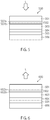
- FIG. 2 is a schematic sectional view showing the structure of a laminate 200 of the embodiment.
- the laminate 200 has a structure comprising a graphene-containing membrane 200a and a graphene oxide film 200b overlaid thereon.
- the graphene-containing membrane 200a has a structure in which one to several layers of sheet-shaped graphene 201 are piled up.
- the graphene 201 has a graphene skeleton to which polyethyleneimine chains are connected.
- the graphene skeleton can be considered to have a surface modified with polyalkyleneimine chains.
- Figure 2 schematically shows graphene skeletons 202 having surfaces modified with polyalkyleneimine chains 203.
- the membrane containing graphene combined with polyethyleneimine chains generally has a small work function, and hence is suitable as a cathode material.
- the graphene oxide film which tends to be negatively charged, is overlaid thereon, the work function tends to increase depending on orientation of the dipoles and consequently the laminate becomes suitable as an anode material. Further, the graphene oxide film also tends to enhance anion-shielding ability.
- the graphene oxide film 200b has a structure in which sheets of graphene oxide 204 are piled up as schematically shown in Figure 2 .
- the graphene oxide film preferably comprises piled one to eight layers of sheet-shaped graphene oxide. The less layers are piled up, the less the work function tends to increase. Further, the more layers are piled up, the more the electric resistance tends to increase.
- the number of the piled layers is preferably 2 to 4.
- the ratio between carbon atoms and oxygen atoms in graphene oxide is 1:0.2 to 1:0.8. If the ratio of oxygen atoms is smaller than 0.2, the film tends to be impaired in transparency and also the work function is liable to less increase. On the other hand, if it is larger than 0.8, the electric resistance tends to increase.
- the work function, which is determined by ultraviolet photoelectron spectroscopy, of the laminate can be controlled to be 4.5 eV or more, and thereby the laminate tends to be improved in performance as an anode.
- the work function is more preferably 4.8 eV or more.
- the laminate can be produced in the following manner. Subsequently to the graphene-containing membrane producing process explained above in the second embodiment, the formed graphene-containing membrane is coated with a dispersion of graphene oxide and then dried to produce the laminate. There are no particular restrictions on the conditions of applying the graphene oxide-containing membrane. For example, they are freely selected from conditions usable in coating for producing the graphene-containing membrane.
- the graphene oxide applied on the graphene-containing membrane may be either the same as a material used for producing the objective graphene- containing membrane or other graphene oxide.
- the step (b) in the graphene-containing membrane producing process can be omitted. This means that the graphene-containing membrane contained in the laminate can be formed without the treatment with a reducing agent.
- FIG. 3 is a schematic sectional view showing the structure of a solar cell 300 (photoelectric conversion device) of the embodiment.
- the solar cell 300 is a device serving as a solar cell in which light energy such as sunlight L coming thereinto is converted into electric power.
- the solar cell 300 comprises a transparent electrode 301 functioning as a cathode, a photoelectric conversion layer 303, and a graphene-containing membrane 302 provided therebetween.
- the cathode in Figure 3 is a transparent electrode, but the anode may be a transparent electrode. Further, both cathode and anode may be transparent electrodes.
- the above graphene-containing membrane 302 contains graphene in which polyethyleneimine chains are connected to the graphene skeleton, which has a ratio of the photoelectron intensity at the energy peak position of C1s orbital to that at the bonding energy on an X-ray photoelectron spectrum measured on an ITO film of 288 eV in a range of 5.5 to 20.
- This graphene-containing membrane tends to improve not only the efficiency but also the working lifetime of the device.
- the graphene-containing membrane 302 preferably has a work function of 4 eV or less.
- the above photoelectric conversion device can have an electrode containing silver.
- the electrode may have a structure comprising an ultrathin silver or silver alloy film sandwiched between transparent conductive oxide films, or otherwise may contain silver- or silver alloy-nanowires. If one electrode is transparent, the other may be a non-transparent silver electrode.
- the silver alloy is preferably silver with Pd, Pt, Au, Sn, Zn or Cu.
- the silver nanowires preferably has an average diameter of 20 to 200 nm. If the diameter is smaller than 20 nm, the stability tends to be lowered. On the other hand, if it is larger than 200 nm, the transparency tends to be lowered.
- the thickness of the ultrathin film and the diameter of nanowires can be determined in the same manner as described above.
- the transparent conductive oxide film can be desirably selected from films of generally-known oxides. Examples thereof include: indium-doped tin oxide ITO, fluorine-doped tin oxide FTO, and aluminum-doped zinc oxide AZO.
- Those metal oxides contain amorphous structures, and the films thereof preferably have thicknesses of 30 to 200 nm. Since they have amorphous structures, it is easy to continuously form even and flat films from them. If the thickness is less than 30 nm, the film tends to have large resistance. On the other hand, if the thickness is more than 200 nm, the film tends to have poor transparency and it tends to take a long time to form the film.
- the thickness is more preferably 35 to 100 nm, further preferably 40 to 70 nm.
- ITO is preferred because the zeta potential thereof in neutral pH is so near to zero as to have small interaction with cations and anions.
- the ultrathin silver or silver alloy film preferably has a thickness of 2 to 20 nm. If it is less than 2 nm, the film tends to have large resistance. On the other hand, if it is more than 20 nm, the film tends to have poor transparency.
- the thickness is more preferably 3 to 15 nm, further preferably 5 to 10 nm.
- the graphene-containing membrane of the embodiment When measured on an ITO film, the graphene-containing membrane of the embodiment preferably shows an X-ray photoelectron spectrum indicating the bonding energy of the peak corresponding to N1s orbital in the range of 399.0 to 399.5 eV. If this condition is satisfied, the membrane tends to contain so many pyridine nitrogen atoms, which are fixed in aromatic rings, that the n-electron system can be expanded enough to lower electric resistance. In addition, if containing many pyridine nitrogen atoms, the membrane tends to have high ability of trapping halogen ions and metal ions.
- the photoelectric conversion device can further comprise a UV-cut layer or a gas-barrier layer.
- ultraviolet absorbers contained in the UV-cut layer include: benzophenones, such as, 2-hydroxy-4-methoxybenzophenone, 2,2-dihydroxy-4-methoxybenzophenone, 2-hydroxy-4-methoxy-2-carboxybenzophenone, and 2-hydroxy-4-n-octoxybenzophenone; benzotriazoles, such as, 2-(2-hydroxy-3,5-di-t-butylphenyl)benzotriazole, 2-(2-hydroxy-5-methylphenyl)benzotriazole, and 2-(2-hydroxy-5-t-octylphenyl)benzotriazole; and salicylic esters, such as, phenyl salicylate and p-octylphenyl salicylate.
- the absorbers are preferably capable of cutting UV light in the wavelength range of 400 nm or less.
- the gas-barrier layer blocks preferably water vapor and oxygen, particularly preferably water vapor.
- This layer is preferably, for example, a film of inorganic substance such as SiN, SiO 2 , SiC, SiO x N y , TiO 2 or Al 2 O 3 . Further, it may be an ultrathin glass sheet.
- the thickness of the gas-barrier layer is preferably 0.01 to 3000 ⁇ m, more preferably 0.1 to 100 ⁇ m. If it is less than 0.01 ⁇ m, the layer often cannot serve fully as a barrier against gases. On the other hand, if the thickness is more than 3000 ⁇ m, the layer tends to be too thick to ensure flexibility or bendability.
- the gas-barrier layer has a water-vapor permeability (moisture permeability) of preferably 10 2 to 10 -6 g/m 2 ⁇ d, more preferably 10 1 to 10 -5 g/m 2 ⁇ d, further preferably 100 to 10 -4 g/m 2 ⁇ d.
- the moisture permeability can be measured according to JIS Z0208 and the like.
- the gas-barrier layer is preferably formed by dry processes.
- Examples of the dry processes for forming the gas-barrier layer include: vacuum deposition processes, such as, resistance heating deposition, electron beam deposition, induction heating deposition, and plasma or ion-beam assisted deposition thereof; sputtering processes, such as, reactive sputtering, ion beam sputtering, and ECR (electron cyclotron resonance) sputtering; PVD (physical vapor deposition) processes, such as, ion plating; and CVD (chemical vapor deposition) processes employing heat, light or plasma.
- vacuum deposition processes such as, resistance heating deposition, electron beam deposition, induction heating deposition, and plasma or ion-beam assisted deposition thereof
- sputtering processes such as, reactive sputtering, ion beam sputtering, and ECR (electron cyclotron resonance) sputtering
- PVD physical vapor deposition
- CVD chemical vapor deposition
- the substrate used in the device of the embodiment is, for example, a transparent substrate made of inorganic materials such as glass or of organic materials such as PET, PEN, polycarbonate and PMMA. Further, aluminum foil and SUS foil are also employable. Preferred are flexible materials because they make the photoelectric conversion device of the embodiment rich in flexibility.
- the photoelectric conversion layer 303 is a semiconductor layer that converts incident light energy into electric power to generate a current.
- the conversion layer 303 generally comprises a p-type semiconductor sub-layer and an N-type semiconductor sub-layer.
- As the photoelectric conversion layer it is also possible to use: a laminate of p-type polymer and n-type material; an inorganic semiconductor such as perovskite type represented by ABX 3 (in which A is a monovalent cation, B is a divalent cation and X is a halogen ion), silicon semiconductor, InGaAs, GaAs, chalcopyrite type, CdTe type, InP type or SiGe type; and a transparent semiconductor such as quantum dots-containing type or dye sensitizing type. Any of the above has enough high efficiency to reduce deterioration of output power.
- the device can further comprise a buffer layer between the conversion layer 303 and the transparent electrode 301.
- the anode (counter electrode) 306 may be a nontransparent metal electrode, but may be a transparent electrode according to the embodiment. Further, the anode 306 may be an ITO glass transparent electrode. In that case, although flexibility is sacrificed, the conversion device can utilize light energy at high efficiency. It is also possible to adopt a metal electrode made of stainless steel, copper, titanium, nickel, chromium, tungsten, gold, silver, molybdenum, tin and/or zinc. That electrode tends to have impaired transparency.
- the device can furthermore comprise a second graphene-containing layer 305, a charge buffer layer or a charge transport layer between the conversion layer 303 and the anode 306.
- the buffer or charge transport layer for anode may be, for example, a layer of vanadium oxide, PEDOT/PSS, P-type polymer, vanadium pentoxide (V 2 O 5 ), 2,2',7,7'-tetrakis[N,N-di(4-methoxyphenyl)amino]-9,9'- spirobifluorene (hereinafter, referred to as "Spiro- OMeTAD”), nickel oxide (NiO) or molybdenum trioxide (MoO 3 ).
- V 2 O 5 vanadium pentoxide
- Spiro- OMeTAD 2,2',7,7'-tetrakis[N,N-di(4-methoxyphenyl)amino]-9,9'- spirobifluorene
- NiO nickel oxide
- MoO 3 molybdenum trioxide
- the buffer or charge transport layer for cathode may be, for example, a layer of lithium fluoride (LiF), calcium (Ca), 6,6'-phenyl-C61-butyric acid methyl ester (C60-PCBM), 6,6'-phenyl-C71-butyric acid methyl ester (hereinafter, referred to as "C70-PCBM”), indene-C60 bisadduct (hereinafter, referred to as "ICBA”), cesium carbonate (Cs 2 CO 3 ), titanium dioxide (TiO 2 ), poly[(9,9-bis(3'-(N,N-dimethylamino)propyl)-2,7-fluorene)-alt-2,7-(9,9-dioctyl-fluorene)] (hereinafter, often referred to as "PFN”), bathocuproine (hereinafter, often referred to as "BCP”), zirconium oxide (ZrO), zinc
- the device can be equipped with a metal oxide layer between the conversion layer and the transparent electrode layer, in particular, adjacently to the graphene-containing membrane.
- the metal oxide layer is, for example, a brookite-type titanium oxide layer or a tin oxide layer. Titanium oxide is known to have three types of crystal structures, namely, rutile-type, anatase-type and brookite-type. Among them, it is preferred to employ a layer containing brookite-type titanium oxide in the embodiment.
- the brookite-type titanium oxide layer has an effect of inhibiting migration of halogen from the conversion layer to the electrode and also migration of metal ions from the electrode to the conversion layer. Consequently, it makes possible to extend the lifetime of the electrode and the device.
- the brookite-type titanium oxide layer preferably comprises nanoparticles of brookite-type titanium oxide, specifically, particles thereof having a mean size of 5 to 30 nm.
- the mean size is determined with a grain-size distribution measuring apparatus.
- Those brookite-type nanoparticles are commercially available from, for example, Kojundo Chemical Lab. Co., Ltd.
- the tin oxide layer can be formed in a manner where a solution of tin oxide dissolved in n-butanol is applied and then heated under a high humid condition.
- the photoelectric conversion device of the embodiment can have a structure sandwiched between transparent electrodes.
- the solar cell having that structure can efficiently utilize light incident from both sides.
- the energy conversion efficiency thereof is generally 5% or more.
- the photoelectric conversion device according to the present embodiment can be used not only as a photocell or solar cell but also as a photosensor.
- FIG. 4 is a schematic sectional view showing an organic EL device 400 (photoelectric conversion device) according to the present embodiment.
- the organic EL device 400 is a device serving as a light-emitting element in which electric energy inputted thereinto is converted into light L.
- the organic EL device 400 comprises a transparent electrode 401 functioning as a cathode, a photoelectric conversion layer 403, and a graphene-containing membrane 402 provided therebetween.
- the cathode in Figure 4 is a transparent electrode, but the anode may be a transparent electrode. Further, both cathode and anode may be transparent electrodes.
- the above graphene-containing membrane 402 contains graphene in which polyethyleneimine chains are connected to the graphene skeleton, which has a ratio of the photoelectron intensity at the energy peak position of C1s orbital to that at the bonding energy on an X-ray photoelectron spectrum measured on an ITO film of 288 eV in a range of 5.5 to 20.
- This graphene-containing membrane tends not only to reduce the driving voltage but also to extend the working lifetime.
- the bonding energy corresponding to N1s orbital is preferably in the range of 399.0 to 399.5 eV.
- the graphene-containing membrane 402 preferably has a work function of 4 eV or less.
- the substrate used in the device of the embodiment is, for example, a transparent substrate made of inorganic materials such as glass or of organic materials such as PET, PEN, polycarbonate and PMMA. Further, aluminum foil and SUS foil are also employable. Preferred are flexible materials because they make the photoelectric conversion device of the embodiment rich in flexibility.
- FIG. 5 is a schematic sectional view showing the structure of a solar cell 500 (photoelectric conversion device) of the embodiment.
- the solar cell 500 is a device serving as a solar cell in which light energy such as sunlight L coming thereinto is converted into electric power.
- the solar cell 500 comprises a transparent electrode 501 functioning as an anode, a photoelectric conversion layer 503, and a laminate 502 which is provided therebetween and which contains a graphene-containing membrane 502a and a graphene oxide film 502b.
- the anode in Figure 5 is a transparent electrode, but the cathode may be a transparent electrode. Further, both cathode and anode may be transparent electrodes.
- the membrane 502a contains graphene combined with polyethyleneimine chains, and generally has a work function small enough to be suitable as a cathode material.
- the work function tends to increase depending on orientation of the dipoles and consequently the laminate becomes suitable as an anode material. Further, the graphene oxide film also tends to enhance anion-shielding ability.
- FIG. 6 is a schematic sectional view showing the structure of an organic EL device 600 (photoelectric conversion device) according to the present embodiment.
- the organic EL device 600 is a device serving as a light-emitting element in which electric energy inputted thereinto is converted into light L.
- the organic EL device 600 comprises a transparent electrode 601 functioning as an anode, a photoelectric conversion layer 603, and a laminate 602 which is provided therebetween and which contains a graphene-containing membrane 602a and a graphene oxide film 602b.
- the anode in Figure 6 is a transparent electrode, but the cathode may be a transparent electrode. Further, both cathode and anode may be transparent electrodes.
- the graphene-containing membrane 602a contains graphene combined with polyethyleneimine chains, and generally has a work function small enough to be suitable as a cathode material.
- the work function tends to increase depending on orientation of the dipoles and consequently the laminate becomes suitable as an anode material. Further, the graphene oxide film also tends to enhance anion-shielding ability.
- a layered structure of ITO (thickness: 45 nm)/silver alloy (thickness: 10 nm)/ITO (thickness: 45 nm) provided on a PET film of about 180 ⁇ m thickness is coated with the above ethanol dispersion by the meniscus coating process with a bar-coater placed at a distance of 500 ⁇ m from the substrate. The coating film is then dried with an infrared heater to produce a graphene-containing membrane.
- a titanium wire is fixed on the graphene-containing membrane formed on the ITO/silver alloy/ITO/PET with silver paste so that they can be electrically connected.
- the bonding part is protected with a silicone tape, and the back surface of the PET film is also protected with a silicone tape.
- the thus-prepared sample is immersed in a 3 mass% aqueous sodium chloride solution and subjected to cyclic voltammetry.
- a sample prepared by only heating with the infrared heater as a sample not comprising the graphene- containing membrane is subjected to cyclic voltammetry in the same manner. From the waveform area on the positive potential side, the reaction amount between chloride ions and silver, namely, the integrated charge amount can be obtained.
- the integrated charge amount Q1 of the sample (1) having the graphene-containing membrane is found to be 3% or less based on that Q0 of the sample (2) not having the graphene-containing membrane. This indicates that chloride ions are shielded in the presence of the graphene-containing membrane.
- a Pt comb-like electrode of 10 ⁇ m-pitch is formed on a glass plate, then drop-coated with the above ethanol dispersion, and thereafter dried at 120°C on a hotplate. Subsequently, the voltage-current curve of the obtained sample is measured by use of a DC power supply.
- Figure 9 shows the result.
- Example 1 The procedure of Example 1 is repeated except for not adding hydrazine hydrate, to produce a graphene- containing membrane.
- Figures 7 and 8 show XPS spectra corresponding to C1s and N1s, respectively.
- the values of R C1s and E N1s are found to be 5.2 and 399.7 eV from Figures 7 and 8 , respectively.
- a Pt comb-like electrode of 10 ⁇ m-pitch is formed on a glass plate, then drop-coated with the above ethanol dispersion and dried at 120°C on a hotplate. Subsequently, the voltage-current curve of the obtained sample is measured by use of a DC power supply.
- Figure 9 shows the result.
- the electric resistance is found to be about twice as large as that of Example 1.
- the work function is found to be 3.8 eV, which is slightly larger than that of Example 1. Those indicate that this sample is inferior to that of Example 1 in suitability as a cathode material.
- Example 1 The procedure of Example 1 is repeated to form a graphene-containing membrane on the layered structure of ITO/silver alloy/ITO.
- the membrane is then coated with an aqueous dispersion of graphene oxide by the meniscus coating process with a bar-coater placed at a distance of 500 ⁇ m from the substrate, and thereafter dried with an infrared heater to produce a laminate.
- the work function is found to be 4.9 eV, which indicates that the laminate is suitable as an anode material.
- Comparative example 1 The procedure of Comparative example 1 is repeated to form a graphene-containing membrane on the layered structure of ITO/silver alloy/ITO.
- the membrane is then coated with an aqueous dispersion of graphene oxide by the meniscus coating process with a bar-coater placed at a distance of 500 ⁇ m from the substrate, and thereafter dried with an infrared heater to produce a laminate.
- the work function is found to be 4.7 eV, which indicates that the laminate is usable as an anode material.
- a layered structure of ITO (thickness: 45 nm)/silver alloy (thickness: 10 nm)/ITO (thickness: 45 nm) provided on a PET film of about 180 ⁇ m thickness is subjected to UV-ozone treatment, and then coated with the above aqueous dispersion by the meniscus coating process with a bar-coater placed at a distance of 500 ⁇ m from the substrate. The coating film is then dried with an infrared heater to produce a graphene-containing membrane.
- R C1s and E N1s are found to be 6.2 and 399.5 eV, respectively. Further, the work function is found to be 3.8 eV, and the electric resistance is found to be about 1.2 times as large as that of Example 1. Although the resistance is slightly larger than that of Example 1, this sample is suitable as a cathode material.
- Example 2 In the same manner as in Example 1, a graphene-containing membrane is formed on a PET film. The membrane is then coated with an isopropanol dispersion of silver nanowires having a diameter of 20 nm by the meniscus coating process with a bar-coater. The coating film is then dried with an infrared heater, and thereafter another graphene-containing membrane is further formed thereon in the same manner as in Example 1. The obtained sample is found to have a work function of 3.7 eV and hence is suitable as a cathode material.
- a titanium wire is fixed on the graphene-containing membrane with silver paste so that they can be electrically connected.
- the bonding part is protected with a silicone tape, and the back surface of the PET film is also protected with a silicone tape.
- the thus-prepared sample is immersed in a 3 mass% aqueous sodium chloride solution and subjected to cyclic voltammetry.
- a sample not having the upper graphene-containing membrane is subjected to cyclic voltammetry in the same manner. From the waveform area on the positive potential side, the reaction amount between chloride ions and silver, namely, the integrated charge amount can be obtained.
- the integrated charge amount Q1 of the sample (1) having the graphene-containing membrane is found to be 1% or less based on that Q0 of the sample (2) only subjected to heating and not having the graphene-containing membrane. This indicates that chloride ions are shielded in the presence of the graphene-containing membrane.
- a solar cell 1000 shown in Figure 10 is produced.
- a layered structure 1002 of ITO (thickness: 45 nm)/silver alloy (thickness: 10 nm)/ITO (thickness: 45 nm) and a graphene-containing membrane 1003 provided thereon are formed on a PET film 1001.
- the graphene-containing membrane is formed in the same manner as in Example 1.
- a toluene solution of C60-PCBN is applied with a bar coater and then dried to form an electron transport layer 1004.
- a chlorobenzene solution containing poly(3-hexyl-thiophene-2,5-diyl) (hereinafter, referred to as "P3HT”) and C60-PCBM is applied with a bar-coater, and dried with infrared light to form a photoelectric conversion layer 1005.
- One surface of a stainless steel foil 1006 provided with an insulating ceramic film formed on the other surface is treated with diluted hydrochloric acid to remove the surface oxide film, then coated with the ethanol dispersion of graphene-containing substance obtained in Example 1 by the meniscus coating process, and subsequently dried with infrared light to form a graphene-containing membrane 1007. Further, an aqueous solution of graphene oxide is applied thereon by the meniscus coating process and then dried with infrared light to form a graphene oxide film 1008.
- a laminate 1009 comprising the graphene-containing membrane and the graphene oxide film is produced.
- an aqueous PEDOT ⁇ PSS solution containing sorbitol is applied with a bar coater and dried with infrared light to form a layer 1010 containing PEDOT ⁇ PSS (thickness: 50 nm).
- This layer functions as both a hole transport layer and an adhesive layer.
- the thus-prepared laminate is then so adhered at 90°C on the photoelectric conversion layer 1005 that the above adhesive layer 1010 may be in contact with the conversion layer 1005.
- UV-cut ink containing 2-hydroxy-4-methoxybenzophenone is screen-printed on the surface of the PET film to form a UV-cut layer 1011, on which a silica film is then formed by vacuum deposition to form a gas-barrier layer 1012. Finally, the boundary is sealed to produce a solar cell 1000.
- the thus-produced solar cell shows an energy conversion efficiency of 6% or more under 1 SUN solar light illumination, and the efficiency deteriorates by less than 5% even after the solar cell is left outdoor for 1 month.
- Example 6 The procedure of Example 6 is repeated except that the ethanol dispersion of graphene-containing substance obtained in Example 1 is replaced with that obtained in Comparative example 1, to produce a solar cell.
- the thus-produced solar cell shows an energy conversion efficiency of 4% or more under 1 SUN solar light illumination.
- An organic EL device 1100 shown in Figure 11 is produced.
- N,N'-di-1-naphthyl-N,N'-diphenyl-1,1'-biphenyl-4,4'-diamine (hereinafter, referred to as "NPD") is vapor-deposited thereon in a thickness of 30 nm to form a hole transport layer 1107. Furthermore, a gold electrode 1108 is formed thereon by sputtering. Finally, the boundary is sealed to produce an organic EL device.
- the obtained organic EL device is of high brightness and hardly deteriorates in output light. Specifically, even after continuous running for 1000 hours, the output falls by 5% or less.
- a transparent solar cell 1200 shown in Figure 12 is produced.
- a graphene-containing membrane 1203 is overlaid on the layered structure 1202 of ITO (thickness: 45 nm)/silver alloy (thickness: 10 nm)/ITO (thickness: 45 nm) provided on a PET film 1201, which is obtained in Example 1, then coated with a toluene solution of C60-PCBN with a bar coater, and thereafter dried to form an electron transport layer 1204.
- a chlorobenzene solution containing poly(3-hexyl-thiophene-2,5-diyl) (hereinafter, referred to as "P3HT”) and C60-PCBM is applied thereon with a bar-coater, and dried with infrared light to form a photoelectric conversion layer 1205, on which an aqueous PEDOT ⁇ PSS solution is then applied with a bar coater and dried with infrared light to form a hole transport layer 1206 (thickness: 50 nm).
- a Teflon sheet is coated with silver nanowires by the meniscus coating process and then dried. Subsequently, the Teflon sheet is brought into contact with the hole transport layer 1206 at 70°C and thereby the silver nanowires are transferred onto the hole transport layer 1206 to produce an upper transparent electrode 1207, which is then covered with a PET film 1208.
- UV-cut ink containing 2-hydroxy-4-methoxybenzo- phenone is screen-printed to form UV-cut layers 1209, on which silica films are then respectively formed by vacuum deposition to form gas-barrier layers 1210. Finally, the boundary is sealed to produce a transparent solar cell 1200.
- the obtained solar cell is transparent and shows an energy conversion efficiency of 3% or more under 1 SUN solar light illumination.
- the efficiency deteriorates by less than 5% even after the solar cell is left outdoor for 1 month.
- a layered structure of ITO (thickness: 45 nm)/silver alloy (thickness: 10 nm)/ITO (thickness: 45 nm) provided on a PET film of about 180 ⁇ m thickness is coated with the above 2-propanol dispersion by the meniscus coating process with a bar-coater placed at a distance of 500 ⁇ m from the substrate.
- the coating film is then dried with an infrared heater to produce a graphene-containing membrane.
- the above graphene-containing membrane is then coated with an aqueous dispersion of graphene oxide by the meniscus coating process with a bar-coater placed at a distance of 500 ⁇ m from the substrate, and thereafter dried with an infrared heater to produce a graphene- containing membrane laminate.
- the work function is found to be 4.8 eV, which indicates that the laminate is suitable as an anode material.
- a solar cell 1300 shown in Figure 13 is produced.
- an aqueous PEDOT ⁇ PSS solution is then applied thereon with a bar coater and dried with infrared light to form a PEDOT ⁇ PSS-containing hole transport layer 1304, and thereafter a chlorobenzene solution containing poly(3-hexylthiophene-2,5-diyl) (hereinafter, referred to as "P3HT") and C60-PCBM is furthermore applied thereon with a bar-coater and dried with infrared light to form a photoelectric conversion layer 1305.
- P3HT poly(3-hexylthiophene-2,5-diyl)
- a 2-propanol dispersion of tin oxide nanoparticles is applied with a bar-coater and then dried to form an electron transport layer 1306. Further, silver is vapor-deposited thereon to form a counter electrode (cathode) 1307, which is then covered with a sealing film 1308 with a gas-barrier layer.
- UV-cut ink containing 2-hydroxy-4-methoxybenzophenone is screen-printed on the surface of the PET film to form a UV-cut layer 1309, on which a silica film is then formed by vacuum deposition to form a gas-barrier layer 1310. Finally, the boundary is sealed to produce a solar cell 1300.
- the obtained solar cell shows an energy conversion efficiency of 5% or more under 1 SUN solar light illumination, and the efficiency deteriorates by less than 5% even after the solar cell is left outdoor for 1 month.
Landscapes
- Physics & Mathematics (AREA)
- Electromagnetism (AREA)
- Optics & Photonics (AREA)
- Chemical & Material Sciences (AREA)
- Engineering & Computer Science (AREA)
- Materials Engineering (AREA)
- Carbon And Carbon Compounds (AREA)
- Photovoltaic Devices (AREA)
- Electroluminescent Light Sources (AREA)
- Laminated Bodies (AREA)
Abstract
Description
- Embodiments of the present disclosure relate to a graphene-containing membrane, a process for producing the membrane, a graphene-containing membrane laminate, and a photoelectric conversion device.
- According to recent increasing of energy consumption, demand for alternative energy replacing fossil energy has been rising as measures to cope with global warming. As a source of the alternative energy, solar cells have been attracted the attention and hence progressively developed. They are studied for various practical applications. From a practical viewpoint, it is particularly desired to improve their flexibility and durability so that they can be installed on various places. However, single crystal silicon solar cells, which are the most basic solar cells, are expensive in cost and it is difficult to produce flexible ones. On the other hand, organic solar cells and organic-inorganic hybrid solar cells, in which many researchers have been lately interested, have room for improvement in durability.
- In addition to the above solar cells, other photoelectric conversion devices, such as organic EL devices and photosensors, have been also researched with the aim of improving their flexibility and durability. Those devices usually comprise ITO films as transparent electrodes. The ITO films are normally formed by sputtering or the like. In order that the ITO films can have high electroconductivity, it is necessary to carry out the sputtering procedure at a high temperature and to anneal thereafter the formed films at a high temperature. However, it is often the case that organic materials cannot be subjected to those procedures at a high temperature. Further, when the ITO films are installed in the devices, metal ions such as indium ion and/or halogen ions may intrude into the active elements such as the photoelectric conversion layers to impair the activity of the devices.
- Meanwhile, it is sometimes the case that low-resistant and high-transparent transparent conductive oxide (TCO)/Ag (or an alloy thereof)/TCO or silver nanowires are adopted as the transparent electrodes. However, in those silver-containing electrodes, silver is often deteriorated by acids or halogens. In addition, silver tends to cause migration and, as a result, may react with water and the like to lower the transparency of the electrode or may migrate into the active elements to impair the activity of the devices. Further, during long term operation, metal ions contained in TCO may diffuse to impair the device activity.
- There are also some cases in which graphene-containing membranes are adopted as the material of transparent electrode. However, although excellent in electroconductivity and stability, graphene-containing membranes are known to have various disadvantages. Specifically, there are many restrictions on their processing. For example, they need to be produced by CVD and the formed graphene membranes must be treated with hydrazine vapor. Graphene membranes can be also formed by wet-coating, but the resultant graphene-containing membranes often have poor electrical properties and hence photoelectric conversion devices comprising them may have unsatisfying performances.
- [Patent document 1]
Japanese Patent Laid-Open No. H12-089786 - In view of the above-mentioned problem, the present embodiment provides a graphene-containing membrane which can be prepared by coating method and has excellent electrical properties, a producing process thereof, graphene-containing membrane laminate, and photoelectric conversion device.
- A graphene-containing membrane according to the first embodiment contains graphene in which polyethyleneimine chains are connected to the graphene skeleton, which has a ratio of the photoelectron intensity at the energy peak position of C1s orbital to that at the bonding energy on an X-ray photoelectron spectrum measured on an ITO film of 288 eV in a range of 5.5 to 20.
- A graphene-containing membrane producing process according to the second embodiment comprises, in this order, the steps of:
- (a) adding polyalkyleneimine into an aqueous dispersion of graphene oxide,
- (b) adding a reducing agent into the dispersion obtained in the above step (a), and then heating the dispersion, and
- (c) coating a substrate with the dispersion obtained in the above step (b).
- A graphene-containing membrane laminate according to the third embodiment has a structure comprising a graphene oxide film overlaid on a membrane containing graphene combined with polyethyleneimine chains.
- A photoelectric conversion device according to the fourth embodiment comprises an anode, a cathode, a photoelectric conversion layer provided between said anode and said cathode, and a graphene-containing membrane provided between said cathode and said photoelectric conversion layer; wherein
said graphene-containing membrane contains graphene in which polyethyleneimine chains are connected to the graphene skeleton and has a ratio of the photoelectron intensity at the energy peak position of C1s orbital to that at the bonding energy on an X-ray photoelectron spectrum measured on an ITO film of 288 eV in a range of 5.5 to 20. - A photoelectric conversion device according to the fifth embodiment comprises an anode, a cathode, a photoelectric conversion layer provided between said anode and said cathode, and such a laminate provided between said anode and said photoelectric conversion layer as has a structure comprising a graphene oxide film overlaid on a membrane containing graphene to which polyethyleneimine chains are connected from the anode side.
-
-
Figure 1 is a schematic sectional view showing the structure of a graphene-containing membrane according to the first embodiment. -
Figure 2 is a schematic sectional view showing the structure of a graphene-containing membrane laminate according to the third embodiment. -
Figure 3 is a schematic sectional view showing the structure of a photoelectric conversion device (solar cell) according to the fourth embodiment. -
Figure 4 is a schematic sectional view showing the structure of another photoelectric conversion device (organic EL device) according to the fourth embodiment. -
Figure 5 is a schematic sectional view showing the structure of a photoelectric conversion device (solar cell) according to the fifth embodiment. -
Figure 6 is a schematic sectional view showing the structure of another photoelectric conversion device (organic EL device) according to the fifth embodiment. -
Figure 7 shows C1s XPS spectra of graphene-containing membranes in Example 1 and Comparative example 1. -
Figure 8 shows N1s XPS spectra of graphene-containing membranes in Example 1 and Comparative example 1. -
Figure 9 shows voltage-current curves of graphene-containing membranes in Example 1 and Comparative example 1. -
Figure 10 is a schematic sectional view showing the structure of a solar cell in Example 6. -
Figure 11 is a schematic sectional view showing the structure of an organic EL device in Example 8. -
Figure 12 is a schematic sectional view showing the structure of a solar cell in Example 9. -
Figure 13 is a schematic sectional view showing the structure of a solar cell in Example 11. - Embodiments will now be explained with reference to the accompanying drawings.
- First, the structure of a graphene-containing membrane according to the first embodiment is explained with reference to
Figure 1 . - A graphene-containing
membrane 100 according to the embodiment has a structure in which one to several layers ofgraphene 101 are piled up. - As schematically shown in
Figure 1 , the graphene-containing membrane of the embodiment has a structure in which one to several layers of sheet-shaped graphene 101 are piled up. There are no particular restrictions on the number of the piled graphene layers, but the number thereof is preferably one to six, more preferably two to four so as to obtain sufficient transparency, electroconductivity and ion shielding effect. - The above graphene has a structure comprising a graphene skeleton to which polyalkyleneimine chains, for example, represented by the following formula, particularly polyethyleneimine chains are connected. In some cases, carbon atoms in the graphene skeleton are partly replaced with nitrogen atoms.

- In the above formula, polyethyleneimine chains are shown as an example of the polyalkyleneimine chains. There are no particular restrictions on the number represented by "n", but n is preferably 2 to 8. Particularly preferred are polyethyleneimine chains of n=2. It is also possible to adopt branched or cyclic polyalkyleneimine chains, as well as, straight ones.
- The graphene shown above can be considered to have a graphene skeleton whose surface is modified with polyalkyleneimine chains.
Figure 1 schematically showsgraphene skeletons 102 having surfaces modified withpolyalkyleneimine chains 103. - The graphene-containing membrane exhibits a characteristic X-ray photoelectron spectrum (i.e., XPS spectrum). Specifically, when measured on an ITO film, the graphene-containing membrane shows an X-ray photoelectron spectrum in which a ratio of the photoelectron intensity at the energy peak position of C1s orbital (IC1s) to that at the bonding energy of 288 eV (I288), namely, a ratio of IC1s/I288 (hereinafter, referred to as "RC1s") is in a range of 5.5 to 20, preferably 6 to 10. The energy peak position of C1s orbital may shift depending on the kind of substituents contained in the graphene-containing membrane, on the content thereof and on the kind of the substrate, but is generally observed at the bonding energy of about 285 eV.
- In general, graphene combined with polyalkyleneimine chains has relatively high insulating property and hence tends to have high electric resistance. However, the graphene-containing membrane of the embodiment, which exhibits the above XPS spectrum, contains C-C bonds (including double bonds) in a high ratio as compared with carbonyl carbons and hence tends to have low electric resistance and small work function.
- As an XPS (X-ray photoelectron spectroscopy) apparatus employed for evaluation, Quantera SXM ([trademark], manufactured by PHI Inc.) can be adopted, for example. This apparatus is equipped with a single crystal-monochromatized AlKa X-ray source, and the X-ray output and X-ray analysis area can be set at 50 W and Φ 200 µm, respectively. The pass energy under the measurement condition is set to be 280.0 eV (1.0 eV/step) for wide scan and 69.0 eV (0.125 eV/step) for narrow scan. The apparatus is also equipped with a charge neutralization gun using both Ar+ and e-. As for the geometry, the angle Θ (angle between the sample surface and the detector) can be set to be Θ=45°. There is an interaction between the substrate and the graphene-containing membrane to be measured, and hence signals in the XPS spectrum may slightly sift depending on the kind of the substrate. In view of that, the XPS signals defined in the embodiment are limited to those obtained by measuring the membrane on an ITO film. As the ITO film, it is possible to adopt, for example, a transparent electrode of ITO/silver alloy/ITO having a surface resistance of about 10 Ω/square (commercially available from OIKE & Co., Ltd.).
- When measured on an ITO film, the graphene-containing membrane of the embodiment preferably shows an X-ray photoelectron spectrum indicating the bonding energy of the peak corresponding to N1s orbital (hereinafter, referred to as "EN1s") in the range of 399.0 to 399.5 eV. If this condition is satisfied, the membrane tends to contain so many pyridine nitrogen atoms, which are fixed in aromatic rings, that the n-electron system can be expanded enough to lower electric resistance. In addition, if containing many pyridine nitrogen atoms, the membrane tends to have high ability of trapping halogen ions and metal ions.
- Further, the graphene-containing membrane of the embodiment preferably has a work function of 4 eV or less, provided that the work function is determined by ultraviolet photoelectron spectroscopy (UPS). If the graphene membrane satisfying this condition is so installed in a photoelectric conversion device that it may be placed between the anode and the photoelectric conversion layer, the anode tends to be improved in function.
- The measurement of ultraviolet photoelectron spectroscopy (UPS) is, for example, carried out with Versa Probe ([trademark], manufactured by PHI Inc.) by use of He I line (21.22 eV) as the light source. For the purpose of precisely detecting electrons of low kinetic energy, the sample stage is exposed to a voltage of -13 V during the measurement. Further, in order to determine the fermi edge, a gold reference having a surface beforehand subjected to Ar ion etching (cleaning) is measured.
- Next, a graphene-containing membrane producing process according to the second embodiment is explained below.
- A graphene-containing membrane producing process of the embodiment comprises, in this order, the steps of:
- (a) adding polyalkyleneimine into an aqueous dispersion of graphene oxide,
- (b) adding a reducing agent into the dispersion obtained in the above step (a), and then heating the dispersion, and
- (c) coating a substrate with the dispersion obtained in the above step (b).
- The aqueous dispersion of graphene oxide in the above step (a) can be prepared by dispersing graphene oxide in an aqueous medium. The graphene oxide used here contains monolayer graphene oxide sheets in an amount of preferably 80 mass% or more, further preferably 90 mass% or more. If satisfying this condition, the graphene oxide can improve homogeneity of the prepared dispersion and also evenness of the coating film. As the aqueous dispersion medium, water such as pure water or ion-exchanged water is adopted. Further, the medium may contain a small amount of aqueous organic solvent such as methanol or ethanol, if necessary. The content of graphene oxide in the dispersion is preferably 0.01 to 1 mass% based on the total mass of the dispersion.
- The mass ratio between the graphene oxide contained in the aqueous dispersion and the polyalkyleneimine to be added therein is preferably 1:3 to 1:20, more preferably 1:7 to 1:15. If the polyalkyleneimine is added in a small amount, dispersibility in the dispersion tends to be lowered. On the other hand, if containing the polyalkyleneimine in a large amount, the resultant film tends to have large electric resistance. The polyalkyleneimine preferably has 2 to 8 carbon atomsr. Examples thereof include polyethyleneimine, polypropyleneimine, and polyethylenepropyleneimine. Among them, polyethyleneimine is preferred. It is also possible to use polyalkyleneimines having various structures, such as, straight chain structure, branched chain structure and cyclic structure. However, polyalkyleneimine of branched chain structure is preferred because it makes easy to improve dispersibility.
- Heating time and temperature are so selected that the polyalkyleneimine can react effectively with the graphene oxide. They can be freely determined according to other conditions, but the mixture is generally heated at 80 to 100°C for 30 to 180 minutes.
- The reducing agent used in the above step (b) is not particularly restricted unless it impairs the effect of the embodiment. The agent is hence selected from reductants capable of working effectively in aqueous dispersions. Example thereof include hydrazine hydrate and sodium borohydride, and hydrazine hydrate is preferred because it provides an appropriate reaction rate.
- When hydrazine hydrate is adopted as the reducing agent, the mass ratio between the graphene oxide and the added hydrazine hydrate is preferably 1:10 to 1:200. If the amount of hydrazine hydrate is small, the graphene oxide is reduced so insufficiently that the resultant graphene-containing membrane tends to have large electric resistance. On the other hand, however, if hydrazine hydrate is added in a large amount, it results in increase of unreacted hydrazine hydrate necessary to be removed after the reaction.
- In the embodiment, it is necessary to carry out the step (b) after the step (a). If the order of those steps is reversed, it is difficult to obtain the aimed graphene-containing membrane.
- As the result of the steps (a) and (b), the aimed graphene is formed in the dispersion. In the step (c), the obtained dispersion can be directly applied on a substate or the like to produce the graphene-containing membrane of the embodiment. However, if necessary, the dispersion also can be subjected to washing or dispersion medium replacement.
- The washing procedure (step (b')) can be carried out, for example, in a manner where graphene formed as the product is separated from the obtained dispersion and then washed with water or the like. Specifically, the dispersion obtained in the step (b) is centrifuged to precipitate formed graphene, which is then recovered and again dispersed in water. This procedure may be repeated twice or more. When graphene is to be precipitated with centrifugation, the condition thereof is preferably 8000 to 15000 rpm. If the rotation rate is small, the yield of the precipitate tends to be lowered. On the other hand, if the rate is large, the precipitate is liable to be contaminated with impurities.
- Prior to the step (c), the precipitated graphene obtained in the step (b') is preferably dispersed in a dispersion medium to prepare a coating solution (step (b")). Examples of the dispersion medium include water and alcohols. However, as the dispersion medium of the coating solution, low molecular alcohols having 1 to 4 carbon atoms are preferred and ethanol or 2-propanol is more preferred. Among them, in view of dispersion stability and safety, ethanol is particularly preferred.
- The reason of that is as follows. Since having a graphene skeleton combined with polyethyleneimine chains, the graphene of the embodiment tends to have high dispersibility in alcohols. In addition, alcohols have smaller surface tension than water, and accordingly the graphene dispersion of alcohol medium has the advantage of easily coating various substrates.
- Subsequently, the obtained dispersion is applied on a substrate (step (c)). In the step (c), the dispersion is preferably applied by bar-coating method. Among various bar-coating processes, it is preferred to adopt a process comprising the steps of: supplying the dispersion into a gap between the substrate and an applicator, so as to form a meniscus between them; and then sliding the substrate or bar-coater to coat said substrate. (Hereinafter, this process is referred to as "meniscus coating process".) In the meniscus coating process, the film thickness can be precisely controlled by adjusting the dispersion concentration, coating speed and meniscus height. Further, this process can be used for large-area coating such as roll-to-roll coating.
- Successively to the step (c), the formed film can be dried according to necessity.
- After the graphene-containing membrane is formed, a dispersion of graphene oxide may be further applied thereon to form a graphene oxide film on the graphene-containing membrane of the embodiment. Here, the graphene oxide film is different from the graphene-containing membrane of the embodiment in that the graphene oxide film is not modified. The unmodified graphene oxide film can increase the work function and also enhance the ion-shielding of the composite laminate. If an aqueous dispersion of graphene oxide is adopted for forming the graphene oxide film, it is easily to form the film evenly because the aqueous dispersion has high affinity with the underlying graphene-containing membrane. However, graphene oxide may be dispersed and applied in an organic solvent such as methanol or ethanol.
- The structure of a graphene-containing membrane laminate (hereinafter, often simply referred to as "laminate") according to the third embodiment is then explained with reference to
Figure 2. Figure 2 is a schematic sectional view showing the structure of alaminate 200 of the embodiment. The laminate 200 has a structure comprising a graphene-containingmembrane 200a and agraphene oxide film 200b overlaid thereon. - As schematically shown in
Figure 2 , the graphene-containingmembrane 200a has a structure in which one to several layers of sheet-shaped graphene 201 are piled up. The graphene 201 has a graphene skeleton to which polyethyleneimine chains are connected. In other words, the graphene skeleton can be considered to have a surface modified with polyalkyleneimine chains.Figure 2 schematically showsgraphene skeletons 202 having surfaces modified withpolyalkyleneimine chains 203. The membrane containing graphene combined with polyethyleneimine chains generally has a small work function, and hence is suitable as a cathode material. However, when the graphene oxide film, which tends to be negatively charged, is overlaid thereon, the work function tends to increase depending on orientation of the dipoles and consequently the laminate becomes suitable as an anode material. Further, the graphene oxide film also tends to enhance anion-shielding ability. - The
graphene oxide film 200b has a structure in which sheets ofgraphene oxide 204 are piled up as schematically shown inFigure 2 . The graphene oxide film preferably comprises piled one to eight layers of sheet-shaped graphene oxide. The less layers are piled up, the less the work function tends to increase. Further, the more layers are piled up, the more the electric resistance tends to increase. The number of the piled layers is preferably 2 to 4. The ratio between carbon atoms and oxygen atoms in graphene oxide is 1:0.2 to 1:0.8. If the ratio of oxygen atoms is smaller than 0.2, the film tends to be impaired in transparency and also the work function is liable to less increase. On the other hand, if it is larger than 0.8, the electric resistance tends to increase. - It is possible to adopt a graphene-containing membrane which has a ratio of the photoelectron intensity at the energy peak position of C1s orbital to that at the bonding energy on an X-ray photoelectron spectrum measured on an ITO film of 288 eV in a range of 5.5 to 20. If that membrane is employed, the laminate tends to have both low electric resistance and small work function.
- The work function, which is determined by ultraviolet photoelectron spectroscopy, of the laminate can be controlled to be 4.5 eV or more, and thereby the laminate tends to be improved in performance as an anode. The work function is more preferably 4.8 eV or more.
- The laminate can be produced in the following manner. Subsequently to the graphene-containing membrane producing process explained above in the second embodiment, the formed graphene-containing membrane is coated with a dispersion of graphene oxide and then dried to produce the laminate. There are no particular restrictions on the conditions of applying the graphene oxide-containing membrane. For example, they are freely selected from conditions usable in coating for producing the graphene-containing membrane. The graphene oxide applied on the graphene-containing membrane may be either the same as a material used for producing the objective graphene- containing membrane or other graphene oxide. When the laminate of the embodiment is to be produced, the step (b) in the graphene-containing membrane producing process can be omitted. This means that the graphene-containing membrane contained in the laminate can be formed without the treatment with a reducing agent.
- The structure of a photoelectric conversion device according to the fourth embodiment is then explained with reference to
Figure 3. Figure 3 is a schematic sectional view showing the structure of a solar cell 300 (photoelectric conversion device) of the embodiment. Thesolar cell 300 is a device serving as a solar cell in which light energy such as sunlight L coming thereinto is converted into electric power. Thesolar cell 300 comprises atransparent electrode 301 functioning as a cathode, aphotoelectric conversion layer 303, and a graphene-containingmembrane 302 provided therebetween. The cathode inFigure 3 is a transparent electrode, but the anode may be a transparent electrode. Further, both cathode and anode may be transparent electrodes. - The above graphene-containing
membrane 302 contains graphene in which polyethyleneimine chains are connected to the graphene skeleton, which has a ratio of the photoelectron intensity at the energy peak position of C1s orbital to that at the bonding energy on an X-ray photoelectron spectrum measured on an ITO film of 288 eV in a range of 5.5 to 20. This graphene-containing membrane tends to improve not only the efficiency but also the working lifetime of the device. The graphene-containingmembrane 302 preferably has a work function of 4 eV or less. - The above photoelectric conversion device can have an electrode containing silver. For example, the electrode may have a structure comprising an ultrathin silver or silver alloy film sandwiched between transparent conductive oxide films, or otherwise may contain silver- or silver alloy-nanowires. If one electrode is transparent, the other may be a non-transparent silver electrode.
- The silver alloy is preferably silver with Pd, Pt, Au, Sn, Zn or Cu. The silver nanowires preferably has an average diameter of 20 to 200 nm. If the diameter is smaller than 20 nm, the stability tends to be lowered. On the other hand, if it is larger than 200 nm, the transparency tends to be lowered. The thickness of the ultrathin film and the diameter of nanowires can be determined in the same manner as described above.
- The transparent conductive oxide film can be desirably selected from films of generally-known oxides. Examples thereof include: indium-doped tin oxide ITO, fluorine-doped tin oxide FTO, and aluminum-doped zinc oxide AZO. Those metal oxides contain amorphous structures, and the films thereof preferably have thicknesses of 30 to 200 nm. Since they have amorphous structures, it is easy to continuously form even and flat films from them. If the thickness is less than 30 nm, the film tends to have large resistance. On the other hand, if the thickness is more than 200 nm, the film tends to have poor transparency and it tends to take a long time to form the film. The thickness is more preferably 35 to 100 nm, further preferably 40 to 70 nm. Among the above oxides, ITO is preferred because the zeta potential thereof in neutral pH is so near to zero as to have small interaction with cations and anions.
- The ultrathin silver or silver alloy film preferably has a thickness of 2 to 20 nm. If it is less than 2 nm, the film tends to have large resistance. On the other hand, if it is more than 20 nm, the film tends to have poor transparency. The thickness is more preferably 3 to 15 nm, further preferably 5 to 10 nm.
- When measured on an ITO film, the graphene-containing membrane of the embodiment preferably shows an X-ray photoelectron spectrum indicating the bonding energy of the peak corresponding to N1s orbital in the range of 399.0 to 399.5 eV. If this condition is satisfied, the membrane tends to contain so many pyridine nitrogen atoms, which are fixed in aromatic rings, that the n-electron system can be expanded enough to lower electric resistance. In addition, if containing many pyridine nitrogen atoms, the membrane tends to have high ability of trapping halogen ions and metal ions.
- The photoelectric conversion device according to the embodiment can further comprise a UV-cut layer or a gas-barrier layer. Examples of ultraviolet absorbers contained in the UV-cut layer include: benzophenones, such as, 2-hydroxy-4-methoxybenzophenone, 2,2-dihydroxy-4-methoxybenzophenone, 2-hydroxy-4-methoxy-2-carboxybenzophenone, and 2-hydroxy-4-n-octoxybenzophenone; benzotriazoles, such as, 2-(2-hydroxy-3,5-di-t-butylphenyl)benzotriazole, 2-(2-hydroxy-5-methylphenyl)benzotriazole, and 2-(2-hydroxy-5-t-octylphenyl)benzotriazole; and salicylic esters, such as, phenyl salicylate and p-octylphenyl salicylate. The absorbers are preferably capable of cutting UV light in the wavelength range of 400 nm or less.
- The gas-barrier layer blocks preferably water vapor and oxygen, particularly preferably water vapor. This layer is preferably, for example, a film of inorganic substance such as SiN, SiO2, SiC, SiOxNy, TiO2 or Al2O3. Further, it may be an ultrathin glass sheet. There are no particular restrictions on the thickness of the gas-barrier layer, but the thickness is preferably 0.01 to 3000 µm, more preferably 0.1 to 100 µm. If it is less than 0.01 µm, the layer often cannot serve fully as a barrier against gases. On the other hand, if the thickness is more than 3000 µm, the layer tends to be too thick to ensure flexibility or bendability. The gas-barrier layer has a water-vapor permeability (moisture permeability) of preferably 102 to 10-6 g/m2·d, more preferably 101 to 10-5 g/m2·d, further preferably 100 to 10-4 g/m2·d. The moisture permeability can be measured according to JIS Z0208 and the like. The gas-barrier layer is preferably formed by dry processes. Examples of the dry processes for forming the gas-barrier layer include: vacuum deposition processes, such as, resistance heating deposition, electron beam deposition, induction heating deposition, and plasma or ion-beam assisted deposition thereof; sputtering processes, such as, reactive sputtering, ion beam sputtering, and ECR (electron cyclotron resonance) sputtering; PVD (physical vapor deposition) processes, such as, ion plating; and CVD (chemical vapor deposition) processes employing heat, light or plasma. Among them, preferred are vacuum deposition processes, in which a film of the layer is formed by deposition in vacuum.
- The substrate used in the device of the embodiment is, for example, a transparent substrate made of inorganic materials such as glass or of organic materials such as PET, PEN, polycarbonate and PMMA. Further, aluminum foil and SUS foil are also employable. Preferred are flexible materials because they make the photoelectric conversion device of the embodiment rich in flexibility.
- The
photoelectric conversion layer 303 is a semiconductor layer that converts incident light energy into electric power to generate a current. Theconversion layer 303 generally comprises a p-type semiconductor sub-layer and an N-type semiconductor sub-layer. As the photoelectric conversion layer, it is also possible to use: a laminate of p-type polymer and n-type material; an inorganic semiconductor such as perovskite type represented by ABX3 (in which A is a monovalent cation, B is a divalent cation and X is a halogen ion), silicon semiconductor, InGaAs, GaAs, chalcopyrite type, CdTe type, InP type or SiGe type; and a transparent semiconductor such as quantum dots-containing type or dye sensitizing type. Any of the above has enough high efficiency to reduce deterioration of output power. - In order to promote or block charge injection, the device can further comprise a buffer layer between the
conversion layer 303 and thetransparent electrode 301. - The anode (counter electrode) 306 may be a nontransparent metal electrode, but may be a transparent electrode according to the embodiment. Further, the
anode 306 may be an ITO glass transparent electrode. In that case, although flexibility is sacrificed, the conversion device can utilize light energy at high efficiency. It is also possible to adopt a metal electrode made of stainless steel, copper, titanium, nickel, chromium, tungsten, gold, silver, molybdenum, tin and/or zinc. That electrode tends to have impaired transparency. - The device can furthermore comprise a second graphene-containing
layer 305, a charge buffer layer or a charge transport layer between theconversion layer 303 and theanode 306. - The buffer or charge transport layer for anode may be, for example, a layer of vanadium oxide, PEDOT/PSS, P-type polymer, vanadium pentoxide (V2O5), 2,2',7,7'-tetrakis[N,N-di(4-methoxyphenyl)amino]-9,9'- spirobifluorene (hereinafter, referred to as "Spiro- OMeTAD"), nickel oxide (NiO) or molybdenum trioxide (MoO3).
- On the other hand, the buffer or charge transport layer for cathode may be, for example, a layer of lithium fluoride (LiF), calcium (Ca), 6,6'-phenyl-C61-butyric acid methyl ester (C60-PCBM), 6,6'-phenyl-C71-butyric acid methyl ester (hereinafter, referred to as "C70-PCBM"), indene-C60 bisadduct (hereinafter, referred to as "ICBA"), cesium carbonate (Cs2CO3), titanium dioxide (TiO2), poly[(9,9-bis(3'-(N,N-dimethylamino)propyl)-2,7-fluorene)-alt-2,7-(9,9-dioctyl-fluorene)] (hereinafter, often referred to as "PFN"), bathocuproine (hereinafter, often referred to as "BCP"), zirconium oxide (ZrO), zinc oxide (ZnO), tungsten trioxide (WO3) or polyethyneimine.
- Further, the device can be equipped with a metal oxide layer between the conversion layer and the transparent electrode layer, in particular, adjacently to the graphene-containing membrane. The metal oxide layer is, for example, a brookite-type titanium oxide layer or a tin oxide layer. Titanium oxide is known to have three types of crystal structures, namely, rutile-type, anatase-type and brookite-type. Among them, it is preferred to employ a layer containing brookite-type titanium oxide in the embodiment. The brookite-type titanium oxide layer has an effect of inhibiting migration of halogen from the conversion layer to the electrode and also migration of metal ions from the electrode to the conversion layer. Consequently, it makes possible to extend the lifetime of the electrode and the device. The brookite-type titanium oxide layer preferably comprises nanoparticles of brookite-type titanium oxide, specifically, particles thereof having a mean size of 5 to 30 nm. Here, the mean size is determined with a grain-size distribution measuring apparatus. Those brookite-type nanoparticles are commercially available from, for example, Kojundo Chemical Lab. Co., Ltd. The tin oxide layer can be formed in a manner where a solution of tin oxide dissolved in n-butanol is applied and then heated under a high humid condition.
- The photoelectric conversion device of the embodiment can have a structure sandwiched between transparent electrodes. The solar cell having that structure can efficiently utilize light incident from both sides. The energy conversion efficiency thereof is generally 5% or more.
- The photoelectric conversion device according to the present embodiment can be used not only as a photocell or solar cell but also as a photosensor.
- With reference to
Figure 4 , the structure of another photoelectric conversion device according to the fourth embodiment is explained below.Figure 4 is a schematic sectional view showing an organic EL device 400 (photoelectric conversion device) according to the present embodiment. Theorganic EL device 400 is a device serving as a light-emitting element in which electric energy inputted thereinto is converted into light L. Theorganic EL device 400 comprises atransparent electrode 401 functioning as a cathode, aphotoelectric conversion layer 403, and a graphene-containingmembrane 402 provided therebetween. The cathode inFigure 4 is a transparent electrode, but the anode may be a transparent electrode. Further, both cathode and anode may be transparent electrodes. - The above graphene-containing
membrane 402 contains graphene in which polyethyleneimine chains are connected to the graphene skeleton, which has a ratio of the photoelectron intensity at the energy peak position of C1s orbital to that at the bonding energy on an X-ray photoelectron spectrum measured on an ITO film of 288 eV in a range of 5.5 to 20. This graphene-containing membrane tends not only to reduce the driving voltage but also to extend the working lifetime. - In the X-ray photoelectron spectrum shown by the graphene-containing membrane measured on an ITO film, the bonding energy corresponding to N1s orbital is preferably in the range of 399.0 to 399.5 eV. Further, the graphene-containing
membrane 402 preferably has a work function of 4 eV or less. - The substrate used in the device of the embodiment is, for example, a transparent substrate made of inorganic materials such as glass or of organic materials such as PET, PEN, polycarbonate and PMMA. Further, aluminum foil and SUS foil are also employable. Preferred are flexible materials because they make the photoelectric conversion device of the embodiment rich in flexibility.
- With reference to
Figure 5 , the structure of a photoelectric conversion device according to the fifth embodiment is then explained below.Figure 5 is a schematic sectional view showing the structure of a solar cell 500 (photoelectric conversion device) of the embodiment. Thesolar cell 500 is a device serving as a solar cell in which light energy such as sunlight L coming thereinto is converted into electric power. Thesolar cell 500 comprises atransparent electrode 501 functioning as an anode, aphotoelectric conversion layer 503, and a laminate 502 which is provided therebetween and which contains a graphene-containingmembrane 502a and agraphene oxide film 502b. The anode inFigure 5 is a transparent electrode, but the cathode may be a transparent electrode. Further, both cathode and anode may be transparent electrodes. - The
membrane 502a contains graphene combined with polyethyleneimine chains, and generally has a work function small enough to be suitable as a cathode material. However, when thegraphene oxide film 502b, which tends to be negatively charged, is overlaid thereon, the work function tends to increase depending on orientation of the dipoles and consequently the laminate becomes suitable as an anode material. Further, the graphene oxide film also tends to enhance anion-shielding ability. - With reference to
Figure 6 , the structure of another photoelectric conversion device according to the fifth embodiment is then explained below.Figure 6 is a schematic sectional view showing the structure of an organic EL device 600 (photoelectric conversion device) according to the present embodiment. Theorganic EL device 600 is a device serving as a light-emitting element in which electric energy inputted thereinto is converted into light L. Theorganic EL device 600 comprises atransparent electrode 601 functioning as an anode, aphotoelectric conversion layer 603, and a laminate 602 which is provided therebetween and which contains a graphene-containingmembrane 602a and agraphene oxide film 602b. The anode inFigure 6 is a transparent electrode, but the cathode may be a transparent electrode. Further, both cathode and anode may be transparent electrodes. - The graphene-containing
membrane 602a contains graphene combined with polyethyleneimine chains, and generally has a work function small enough to be suitable as a cathode material. However, when thegraphene oxide film 602b, which tends to be negatively charged, is overlaid thereon, the work function tends to increase depending on orientation of the dipoles and consequently the laminate becomes suitable as an anode material. Further, the graphene oxide film also tends to enhance anion-shielding ability. - The embodiments are explained below by use of the following examples.
- Into 30 g of a graphene oxide aqueous dispersion containing monolayer graphene oxide sheets in an amount of 80 mass% or more (concentration: 0.05 wt%), 2 g of a branched polyethyleneimine aqueous solution (concentration: 10 wt%) is added. The mixture is heated at 90°C for 1 hour, then 2 g of hydrazine hydrate is added therein, and thereafter the mixture is further heated at 90°C for 1 hour. The resultant mixture is centrifuged at 12000 rpm to obtain precipitates, which are then dispersed again in water. The dispersion is centrifuged at 12000 rpm to obtain precipitates. This procedure is repeated twice to remove unreacted polyethyleneimine and hydrazine hydrate. The obtained precipitates are dried and dispersed in ethanol to prepare an ethanol dispersion of graphene-containing substance.
- A layered structure of ITO (thickness: 45 nm)/silver alloy (thickness: 10 nm)/ITO (thickness: 45 nm) provided on a PET film of about 180 µm thickness is coated with the above ethanol dispersion by the meniscus coating process with a bar-coater placed at a distance of 500 µm from the substrate. The coating film is then dried with an infrared heater to produce a graphene-containing membrane.
- From XPS measurement, the content of the nitrogen atoms is found to be 12% of the carbon atoms. In this case, the membrane contains many nitrogen atoms coming from the polyethyleneimine. From IR spectroscopy, it is found that the graphene is linked with an alkyl chain. Further, from UPS measurement, the work function is found to be 3.7 eV.
Figures 7 and8 show XPS spectra corresponding to C1s and N1s, respectively. The values of RC1s and EN1s are found to be 7.1 and 399.3 eV fromFigures 7 and8 , respectively. - A titanium wire is fixed on the graphene-containing membrane formed on the ITO/silver alloy/ITO/PET with silver paste so that they can be electrically connected. The bonding part is protected with a silicone tape, and the back surface of the PET film is also protected with a silicone tape. The thus-prepared sample is immersed in a 3 mass% aqueous sodium chloride solution and subjected to cyclic voltammetry. In the meantime, a sample prepared by only heating with the infrared heater as a sample not comprising the graphene- containing membrane is subjected to cyclic voltammetry in the same manner. From the waveform area on the positive potential side, the reaction amount between chloride ions and silver, namely, the integrated charge amount can be obtained. As a result, the integrated charge amount Q1 of the sample (1) having the graphene-containing membrane is found to be 3% or less based on that Q0 of the sample (2) not having the graphene-containing membrane. This indicates that chloride ions are shielded in the presence of the graphene-containing membrane.
- Independently, a Pt comb-like electrode of 10 µm-pitch is formed on a glass plate, then drop-coated with the above ethanol dispersion, and thereafter dried at 120°C on a hotplate. Subsequently, the voltage-current curve of the obtained sample is measured by use of a DC power supply.
Figure 9 shows the result. - The procedure of Example 1 is repeated except for not adding hydrazine hydrate, to produce a graphene- containing membrane.
Figures 7 and8 show XPS spectra corresponding to C1s and N1s, respectively. The values of RC1s and EN1s are found to be 5.2 and 399.7 eV fromFigures 7 and8 , respectively. - Independently, a Pt comb-like electrode of 10 µm-pitch is formed on a glass plate, then drop-coated with the above ethanol dispersion and dried at 120°C on a hotplate. Subsequently, the voltage-current curve of the obtained sample is measured by use of a DC power supply.
Figure 9 shows the result. The electric resistance is found to be about twice as large as that of Example 1. Further, the work function is found to be 3.8 eV, which is slightly larger than that of Example 1. Those indicate that this sample is inferior to that of Example 1 in suitability as a cathode material. - The procedure of Example 1 is repeated to form a graphene-containing membrane on the layered structure of ITO/silver alloy/ITO. The membrane is then coated with an aqueous dispersion of graphene oxide by the meniscus coating process with a bar-coater placed at a distance of 500 µm from the substrate, and thereafter dried with an infrared heater to produce a laminate. From UPS measurement, the work function is found to be 4.9 eV, which indicates that the laminate is suitable as an anode material.
- The procedure of Comparative example 1 is repeated to form a graphene-containing membrane on the layered structure of ITO/silver alloy/ITO. The membrane is then coated with an aqueous dispersion of graphene oxide by the meniscus coating process with a bar-coater placed at a distance of 500 µm from the substrate, and thereafter dried with an infrared heater to produce a laminate. From UPS measurement, the work function is found to be 4.7 eV, which indicates that the laminate is usable as an anode material.
- Into 30 g of a graphene oxide aqueous dispersion containing monolayer graphene oxide sheets in an amount of 80 mass% or more (concentration: 0.05 wt%), 0.5 g of a branched polyethyleneimine aqueous solution (concentration: 10 wt%) is added. The mixture is heated at 90°C for 1 hour, then 0.2 g of hydrazine hydrate is added therein, and thereafter the mixture is further heated at 90°C for 30 hours. The resultant mixture is centrifuged at 12000 rpm to obtain precipitates, which are then dispersed again in water. The dispersion is centrifuged at 12000 rpm to obtain precipitates. This procedure is repeated twice to remove unreacted polyethyleneimine and hydrazine hydrate. The obtained precipitates are dried and dispersed in water to prepare an aqueous dispersion of graphene-containing substance.
- A layered structure of ITO (thickness: 45 nm)/silver alloy (thickness: 10 nm)/ITO (thickness: 45 nm) provided on a PET film of about 180 µm thickness is subjected to UV-ozone treatment, and then coated with the above aqueous dispersion by the meniscus coating process with a bar-coater placed at a distance of 500 µm from the substrate. The coating film is then dried with an infrared heater to produce a graphene-containing membrane.
- The values of RC1s and EN1s are found to be 6.2 and 399.5 eV, respectively. Further, the work function is found to be 3.8 eV, and the electric resistance is found to be about 1.2 times as large as that of Example 1. Although the resistance is slightly larger than that of Example 1, this sample is suitable as a cathode material.
- In the same manner as in Example 1, a graphene-containing membrane is formed on a PET film. The membrane is then coated with an isopropanol dispersion of silver nanowires having a diameter of 20 nm by the meniscus coating process with a bar-coater. The coating film is then dried with an infrared heater, and thereafter another graphene-containing membrane is further formed thereon in the same manner as in Example 1. The obtained sample is found to have a work function of 3.7 eV and hence is suitable as a cathode material.
- A titanium wire is fixed on the graphene-containing membrane with silver paste so that they can be electrically connected. The bonding part is protected with a silicone tape, and the back surface of the PET film is also protected with a silicone tape. The thus-prepared sample is immersed in a 3 mass% aqueous sodium chloride solution and subjected to cyclic voltammetry. In the meantime, a sample not having the upper graphene-containing membrane is subjected to cyclic voltammetry in the same manner. From the waveform area on the positive potential side, the reaction amount between chloride ions and silver, namely, the integrated charge amount can be obtained. As a result, the integrated charge amount Q1 of the sample (1) having the graphene-containing membrane is found to be 1% or less based on that Q0 of the sample (2) only subjected to heating and not having the graphene-containing membrane. This indicates that chloride ions are shielded in the presence of the graphene-containing membrane.
- A
solar cell 1000 shown inFigure 10 is produced. - A
layered structure 1002 of ITO (thickness: 45 nm)/silver alloy (thickness: 10 nm)/ITO (thickness: 45 nm) and a graphene-containingmembrane 1003 provided thereon are formed on aPET film 1001. The graphene-containing membrane is formed in the same manner as in Example 1. On the membrane, a toluene solution of C60-PCBN is applied with a bar coater and then dried to form anelectron transport layer 1004. Subsequently, a chlorobenzene solution containing poly(3-hexyl-thiophene-2,5-diyl) (hereinafter, referred to as "P3HT") and C60-PCBM is applied with a bar-coater, and dried with infrared light to form aphotoelectric conversion layer 1005. - One surface of a
stainless steel foil 1006 provided with an insulating ceramic film formed on the other surface is treated with diluted hydrochloric acid to remove the surface oxide film, then coated with the ethanol dispersion of graphene-containing substance obtained in Example 1 by the meniscus coating process, and subsequently dried with infrared light to form a graphene-containing membrane 1007. Further, an aqueous solution of graphene oxide is applied thereon by the meniscus coating process and then dried with infrared light to form a graphene oxide film 1008. Thus, a laminate 1009 comprising the graphene-containing membrane and the graphene oxide film is produced. - On the
laminate 1009, an aqueous PEDOT·PSS solution containing sorbitol is applied with a bar coater and dried with infrared light to form a layer 1010 containing PEDOT·PSS (thickness: 50 nm). This layer functions as both a hole transport layer and an adhesive layer. - The thus-prepared laminate is then so adhered at 90°C on the
photoelectric conversion layer 1005 that the above adhesive layer 1010 may be in contact with theconversion layer 1005. UV-cut ink containing 2-hydroxy-4-methoxybenzophenone is screen-printed on the surface of the PET film to form a UV-cut layer 1011, on which a silica film is then formed by vacuum deposition to form a gas-barrier layer 1012. Finally, the boundary is sealed to produce asolar cell 1000. - The thus-produced solar cell shows an energy conversion efficiency of 6% or more under 1 SUN solar light illumination, and the efficiency deteriorates by less than 5% even after the solar cell is left outdoor for 1 month.
- The procedure of Example 6 is repeated except that the ethanol dispersion of graphene-containing substance obtained in Example 1 is replaced with that obtained in Comparative example 1, to produce a solar cell.
- The thus-produced solar cell shows an energy conversion efficiency of 4% or more under 1 SUN solar light illumination.
- An
organic EL device 1100 shown inFigure 11 is produced. - The layered structure of graphene-containing
membrane 1102/silver nanowires 1103/graphene- containingmembrane 1104 formed on aPET film 1101, which is obtained in Example 5, is coated with a toluene solution of C60-PCBN with a bar coater and then dried to form anelectron transport layer 1105, on which tris(8-hydroxyquinoline)aluminum (Alq3) (40 nm) is vapor-deposited to form aphotoelectric conversion layer 1106. Further, N,N'-di-1-naphthyl-N,N'-diphenyl-1,1'-biphenyl-4,4'-diamine (hereinafter, referred to as "NPD") is vapor-deposited thereon in a thickness of 30 nm to form ahole transport layer 1107. Furthermore, agold electrode 1108 is formed thereon by sputtering. Finally, the boundary is sealed to produce an organic EL device. - The obtained organic EL device is of high brightness and hardly deteriorates in output light. Specifically, even after continuous running for 1000 hours, the output falls by 5% or less.
- A transparent
solar cell 1200 shown inFigure 12 is produced. - A graphene-containing
membrane 1203 is overlaid on thelayered structure 1202 of ITO (thickness: 45 nm)/silver alloy (thickness: 10 nm)/ITO (thickness: 45 nm) provided on aPET film 1201, which is obtained in Example 1, then coated with a toluene solution of C60-PCBN with a bar coater, and thereafter dried to form anelectron transport layer 1204. Subsequently, a chlorobenzene solution containing poly(3-hexyl-thiophene-2,5-diyl) (hereinafter, referred to as "P3HT") and C60-PCBM is applied thereon with a bar-coater, and dried with infrared light to form aphotoelectric conversion layer 1205, on which an aqueous PEDOT·PSS solution is then applied with a bar coater and dried with infrared light to form a hole transport layer 1206 (thickness: 50 nm). - Independently, a Teflon sheet is coated with silver nanowires by the meniscus coating process and then dried. Subsequently, the Teflon sheet is brought into contact with the
hole transport layer 1206 at 70°C and thereby the silver nanowires are transferred onto thehole transport layer 1206 to produce an uppertransparent electrode 1207, which is then covered with aPET film 1208. - On both surfaces of the thus-obtained laminate, UV-cut ink containing 2-hydroxy-4-methoxybenzo- phenone is screen-printed to form UV-cut layers 1209, on which silica films are then respectively formed by vacuum deposition to form gas-
barrier layers 1210. Finally, the boundary is sealed to produce a transparentsolar cell 1200. - The obtained solar cell is transparent and shows an energy conversion efficiency of 3% or more under 1 SUN solar light illumination. The efficiency deteriorates by less than 5% even after the solar cell is left outdoor for 1 month.
- Into 30 g of a graphene oxide aqueous dispersion containing monolayer graphene oxide sheets in an amount of 80 mass% or more (concentration: 0.05 wt%), 2 g of a branched polyethyleneimine aqueous solution (concentration: 10 wt%) is added. The mixture is heated at 90°C for 1.5 hours, then 2 g of 5% sodium borohydride aqueous solution is added therein, and thereafter the mixture is further heated at 90°C for 30 minutes. The resultant mixture is centrifuged at 12000 rpm to obtain precipitates, which are then dispersed again in water. The dispersion is centrifuged at 12000 rpm to obtain precipitates. This procedure is repeated twice to remove unreacted polyethyleneimine and sodium borohydride. The obtained precipitates are dried and dispersed in 2-propanol to prepare a 2-propanol dispersion of graphene-containing substance.
- A layered structure of ITO (thickness: 45 nm)/silver alloy (thickness: 10 nm)/ITO (thickness: 45 nm) provided on a PET film of about 180 µm thickness is coated with the above 2-propanol dispersion by the meniscus coating process with a bar-coater placed at a distance of 500 µm from the substrate. The coating film is then dried with an infrared heater to produce a graphene-containing membrane.
- The above graphene-containing membrane is then coated with an aqueous dispersion of graphene oxide by the meniscus coating process with a bar-coater placed at a distance of 500 µm from the substrate, and thereafter dried with an infrared heater to produce a graphene- containing membrane laminate. From UPS measurement, the work function is found to be 4.8 eV, which indicates that the laminate is suitable as an anode material.
- A
solar cell 1300 shown inFigure 13 is produced. - The
layered structure 1302 of ITO (thickness: 45 nm)/silver alloy (thickness: 10 nm)/ITO (thickness: 45 nm) provided on aPET film 1301, which is obtained in Example 10, and a graphene-containingmembrane laminate 1303 comprising a graphene-containingmembrane 1303/a graphene oxide film are stacked. Further, an aqueous PEDOT·PSS solution is then applied thereon with a bar coater and dried with infrared light to form a PEDOT·PSS-containinghole transport layer 1304, and thereafter a chlorobenzene solution containing poly(3-hexylthiophene-2,5-diyl) (hereinafter, referred to as "P3HT") and C60-PCBM is furthermore applied thereon with a bar-coater and dried with infrared light to form aphotoelectric conversion layer 1305. - On the above
photoelectric conversion layer 1305, a 2-propanol dispersion of tin oxide nanoparticles is applied with a bar-coater and then dried to form anelectron transport layer 1306. Further, silver is vapor-deposited thereon to form a counter electrode (cathode) 1307, which is then covered with asealing film 1308 with a gas-barrier layer. - UV-cut ink containing 2-hydroxy-4-methoxybenzophenone is screen-printed on the surface of the PET film to form a UV-
cut layer 1309, on which a silica film is then formed by vacuum deposition to form a gas-barrier layer 1310. Finally, the boundary is sealed to produce asolar cell 1300. - The obtained solar cell shows an energy conversion efficiency of 5% or more under 1 SUN solar light illumination, and the efficiency deteriorates by less than 5% even after the solar cell is left outdoor for 1 month.
- While certain embodiments have been described, these embodiments have been presented by way of example only, and are not intended to limit the scope of the inventions. Indeed, the novel methods and systems described herein may be embodied in a variety of other forms; furthermore, various omissions, substitutions and changes in the form of the methods and systems described herein may be made without departing from the spirit of the inventions. The accompanying claims and their equivalents are intended to cover such forms or modifications as would fail within the scope and spirit of the invention.
-
- 100
- graphene-containing membrane
- 101
- graphene
- 102
- graphene skeletons
- 103
- polyethyleneimine chains
- 200
- graphene-containing membrane laminate
- 200a
- graphene-containing membrane
- 200b
- graphene oxide film
- 201
- graphene
- 202
- graphene skeletons
- 203
- polyethyleneimine chains
- 204
- graphene oxide
- 300
- solar cell
- 301
- transparent electrode
- 302
- graphene-containing membrane
- 303
- photoelectric conversion layer
- 304
- cathode
- 305
- second graphene-containing membrane
- 306
- graphene oxide film
- 400
- organic EL device
- 401
- transparent electrode
- 500
- solar cell
- 501
- transparent electrode
- 502
- graphene-containing membrane laminate
- 502a
- graphene-containing membrane
- 502b
- graphene oxide film
- 503
- photoelectric conversion layer
- 504
- anode
- 600
- organic EL device
- 601
- transparent electrode
- 602
- graphene-containing membrane laminate
- 602a
- graphene-containing membrane
- 602b
- graphene oxide film
- 603
- photoelectric conversion layer
- 604
- anode
- 1000
- solar cell
- 1001
- PET film
- 1002
- layered structure of ITO/silver alloy/ITO
- 1003
- graphene-containing membrane
- 1004
- electron transport layer
- 1005
- photoelectric conversion layer
- 1006
- stainless steel foil
- 1007
- graphene-containing membrane
- 1008
- graphene oxide film
- 1009
- graphene-containing membrane laminate
- 1010
- hole transport layer/adhesive layer
- 1011
- UV-cut layer
- 1012
- gas-barrier layer
- 1100
- organic EL device
- 1101
- PET film
- 1102
- graphene-containing membrane
- 1103
- silver nanowires
- 1104
- graphene-containing membrane
- 1105
- electron transport layer
- 1106
- photoelectric conversion layer
- 1107
- hole transport layer
- 1108
- gold electrode
- 1200
- transparent solar cell
- 1201
- PET film
- 1202
- layered structure of ITO/silver alloy/ITO
- 1203
- graphene-containing membrane
- 1204
- electron transport layer
- 1205
- photoelectric conversion layer
- 1206
- hole transport layer
- 1207
- upper transparent electrode
- 1208
- PET film
- 1209
- UV-cut layer
- 1210
- gas-barrier layer
- 1300
- solar cell
- 1301
- PET film
- 1302
- layered structure of ITO/silver alloy/ITO
- 1303
- graphene-containing membrane laminate
- 1304
- hole transport layer
- 1305
- photoelectric conversion layer
- 1306
- electron transport layer
- 1307
- counter electrode
- 1308
- sealing film
- 1309
- UV-cut layer
- 1310
- gas-barrier layer
Claims (19)
- A graphene-containing membrane containing graphene in which polyethyleneimine chains are connected to the graphene skeleton; which has a ratio of the photoelectron intensity at the energy peak position of C1s orbital to that at the bonding energy on an X-ray photoelectron spectrum measured on an ITO film of 288 eV in a range of 5.5 to 20.
- The graphene-containing membrane according to claim 1, wherein said X-ray photoelectron spectrum measured on an ITO film indicates the bonding energy of the peak corresponding to N1s orbital in the range of 399.0 to 399.5 eV.
- The graphene-containing membrane according to claim 1 or 2, which has a work function of 4 eV or less according to ultraviolet photoelectron spectroscopy measurement.
- A graphene-containing membrane producing process comprising, in this order, the steps of:(a) adding polyalkyleneimine into an aqueous dispersion of graphene oxide,(b) adding a reducing agent into the dispersion obtained in the above step (a), and then heating the dispersion, and(c) coating a substrate with the dispersion obtained in the above step (b).
- The process according to claim 4, further comprising the step of:
(b') washing the dispersed product formed in said step (b) between said steps of (b) and (c). - The process according to claim 5, furthermore comprising the step of:
(b") dispersing the product obtained in said step (b') in a low molecular weight alcohol having 1 to 4 carbon atoms, so as to produce a coating solution
between said steps of (b') and (c). - The process according to any one of claims 4 to 6, wherein said step (c) is carried out by a bar-coating process comprising the steps of: supplying the dispersion obtained in said step (b) into a gap between said substrate and an applicator, so as to form a meniscus between them; and then sliding said substrate or said applicator.
- The process according to claim any one of claims 4 to7, wherein said reducing agent is hydrazine hydrate.
- A graphene-containing membrane laminate which has a structure comprising a graphene oxide film overlaid on a membrane containing graphene combined with polyethyleneimine chains.
- The graphene-containing membrane laminate according to claim 9, wherein said membrane containing graphene has a ratio of the photoelectron intensity at the energy peak position of C1s orbital to that at the bonding energy on an X-ray photoelectron spectrum measured on an ITO film of 288 eV in a range of 5.5 to 20.
- The graphene-containing membrane laminate according to claim 9 or 10, which has a work function of 4.5 eV or more according to ultraviolet photoelectron spectroscopy measurement.
- A photoelectric conversion device comprising an anode, a cathode, a photoelectric conversion layer provided between said anode and said cathode, and a graphene-containing membrane provided between said cathode and said photoelectric conversion layer; wherein
said graphene-containing membrane contains graphene in which polyethyleneimine chains are connected to the graphene skeleton and has a ratio of the photoelectron intensity at the energy peak position of C1s orbital to that at the bonding energy on an X-ray photoelectron spectrum measured on an ITO film of 288 eV in a range of 5.5 to 20. - The device according to claim 12, wherein said X-ray photoelectron spectrum measured on an ITO film indicates the bonding energy corresponding to N1s orbital in the range of 399.0 to 399.5 eV.
- The device according to claim 12 or 13, wherein said graphene-containing membrane has a work function of 4 eV or less according to ultraviolet photoelectron spectroscopy measurement.
- A photoelectric conversion device comprising an anode, a cathode, a photoelectric conversion layer provided between said anode and said cathode, and such a laminate provided between said anode and said photoelectric conversion layer as has a structure comprising a graphene oxide film overlaid on a membrane containing graphene to which polyethyleneimine chains are connected from the anode side.
- The device according to claim 15, wherein said laminate has a work function of 4.5 eV or more according to ultraviolet photoelectron spectroscopy measurement.
- The device according to claim 15 or 16, wherein said membrane containing graphene has a ratio of the photoelectron intensity at the energy peak position of C1s orbital to that at the bonding energy on an X-ray photoelectron spectrum measured on an ITO film of 288 eV in a range of 5.5 to 20.
- The device according to any one of claims 12 to 17, wherein at least one of said anode and said cathode contains silver.
- The device according to any one of claims 12 to 18, wherein at least one of said anode and said cathode is a transparent electrode containing indium-tin oxide.
Priority Applications (1)
| Application Number | Priority Date | Filing Date | Title |
|---|---|---|---|
| EP24161709.1A EP4358645A3 (en) | 2019-03-05 | 2019-03-05 | Graphene-containing film, production method thereof, graphene-containing film laminate, and photoelectric conversion element |
Applications Claiming Priority (1)
| Application Number | Priority Date | Filing Date | Title |
|---|---|---|---|
| PCT/JP2019/008551 WO2020178974A1 (en) | 2019-03-05 | 2019-03-05 | Graphene-containing film, production method thereof, graphene-containing film laminate, and photoelectric conversion element |
Related Child Applications (2)
| Application Number | Title | Priority Date | Filing Date |
|---|---|---|---|
| EP24161709.1A Division EP4358645A3 (en) | 2019-03-05 | 2019-03-05 | Graphene-containing film, production method thereof, graphene-containing film laminate, and photoelectric conversion element |
| EP24161709.1A Division-Into EP4358645A3 (en) | 2019-03-05 | 2019-03-05 | Graphene-containing film, production method thereof, graphene-containing film laminate, and photoelectric conversion element |
Publications (3)
| Publication Number | Publication Date |
|---|---|
| EP3937267A1 true EP3937267A1 (en) | 2022-01-12 |
| EP3937267A4 EP3937267A4 (en) | 2023-01-18 |
| EP3937267B1 EP3937267B1 (en) | 2024-11-06 |
Family
ID=72338460
Family Applications (2)
| Application Number | Title | Priority Date | Filing Date |
|---|---|---|---|
| EP19915584.7A Active EP3937267B1 (en) | 2019-03-05 | 2019-03-05 | Graphene-containing film, production method thereof, graphene-containing film laminate, and photoelectric conversion element |
| EP24161709.1A Pending EP4358645A3 (en) | 2019-03-05 | 2019-03-05 | Graphene-containing film, production method thereof, graphene-containing film laminate, and photoelectric conversion element |
Family Applications After (1)
| Application Number | Title | Priority Date | Filing Date |
|---|---|---|---|
| EP24161709.1A Pending EP4358645A3 (en) | 2019-03-05 | 2019-03-05 | Graphene-containing film, production method thereof, graphene-containing film laminate, and photoelectric conversion element |
Country Status (5)
| Country | Link |
|---|---|
| US (2) | US11387375B2 (en) |
| EP (2) | EP3937267B1 (en) |
| JP (1) | JP7119102B2 (en) |
| CN (1) | CN112154550A (en) |
| WO (1) | WO2020178974A1 (en) |
Families Citing this family (11)
| Publication number | Priority date | Publication date | Assignee | Title |
|---|---|---|---|---|
| DE102018101700A1 (en) * | 2018-01-25 | 2019-07-25 | Osram Opto Semiconductors Gmbh | Optoelectronic semiconductor component and method for producing an optoelectronic semiconductor component |
| WO2021176518A1 (en) | 2020-03-02 | 2021-09-10 | 株式会社 東芝 | Transparent electrode, method for producing transparent electrode, and photoelectric conversion element provided with transparent electrode |
| EP4213220A4 (en) * | 2020-09-09 | 2024-06-05 | Kabushiki Kaisha Toshiba | Transparent electrode, method for manufacturing transparent electrode, and electronic device |
| EP4302882A4 (en) | 2021-03-04 | 2025-01-29 | Kabushiki Kaisha Toshiba | Coating apparatus and coating method |
| WO2023009962A2 (en) * | 2021-07-30 | 2023-02-02 | Alliance For Sustainable Energy, Llc | Highly efficient and durable on-device metal sequestering tapes for solar cells and modules |
| JP7554344B2 (en) | 2021-08-19 | 2024-09-19 | 株式会社東芝 | Conductive member, electronic device, and method for manufacturing conductive member |
| CN114005902B (en) * | 2021-11-05 | 2023-08-22 | 电子科技大学中山学院 | Inverted multi-junction solar cell based on GaAs substrate |
| WO2024105715A1 (en) * | 2022-11-14 | 2024-05-23 | 株式会社東芝 | Solar cell sheet |
| JPWO2025032715A1 (en) * | 2023-08-08 | 2025-02-13 | ||
| CN117288809B (en) * | 2023-09-25 | 2024-04-12 | 湖南星硕传感科技有限公司 | Carbon-based hydrogen sensor chip |
| JP2025104516A (en) * | 2023-12-28 | 2025-07-10 | 株式会社アイシン | Perovskite Solar Cells |
Family Cites Families (27)
| Publication number | Priority date | Publication date | Assignee | Title |
|---|---|---|---|---|
| JPH0289786A (en) | 1988-09-28 | 1990-03-29 | Toshiba Corp | Device for detecting abnormal lowering of oil viscosity of hydraulic elevator |
| JP2000089786A (en) | 1998-09-08 | 2000-03-31 | Nippon Hoso Kyokai <Nhk> | Method and apparatus for correcting speech recognition result |
| TW201012749A (en) * | 2008-08-19 | 2010-04-01 | Univ Rice William M | Methods for preparation of graphene nanoribbons from carbon nanotubes and compositions, thin films and devices derived therefrom |
| WO2010030511A2 (en) | 2008-09-09 | 2010-03-18 | Vanguard Solar, Inc. | Solar cells and photodetectors with semiconducting nanostructures |
| US8636830B2 (en) | 2010-06-11 | 2014-01-28 | William Marsh Rice University | Aliphatic amine based nanocarbons for the absorption of carbon dioxide |
| US20120021224A1 (en) * | 2010-07-23 | 2012-01-26 | Clean Energy Labs, Llc | Graphene/graphene oxide platelet composite membranes and methods and devices thereof |
| JP5627390B2 (en) | 2010-10-22 | 2014-11-19 | 株式会社東芝 | Photoelectric conversion element and manufacturing method thereof |
| KR101469450B1 (en) * | 2011-03-02 | 2014-12-05 | 그래핀스퀘어 주식회사 | N-doping method of graphene |
| JP5961355B2 (en) * | 2011-08-31 | 2016-08-02 | 国立大学法人埼玉大学 | Photo-induced charge separation device, photovoltaic cell and method for producing the same |
| US9011968B2 (en) * | 2011-09-16 | 2015-04-21 | Empire Technology Development Llc | Alteration of graphene defects |
| JP2013211212A (en) * | 2012-03-30 | 2013-10-10 | Toshiba Corp | Laminated electrode, manufacturing method therefor and photoelectric conversion element |
| US10858296B1 (en) * | 2012-06-27 | 2020-12-08 | James J. Myrick | Energetics, compositions, manufacture and applications |
| JP2014170826A (en) * | 2013-03-04 | 2014-09-18 | Dainippon Screen Mfg Co Ltd | Wiring structure, method for forming wiring, and electronic device |
| EP3054459B1 (en) | 2013-10-04 | 2018-07-11 | ONES (Organic Nano Electronic System) Co., LTD | Electrode having excellent light transmittance and method for manufacturing same |
| TWI522499B (en) | 2014-03-19 | 2016-02-21 | 國立中興大學 | A method of modifying the reduced graphene layer on the surface of the substrate |
| US20170125171A1 (en) | 2014-04-23 | 2017-05-04 | Lg Chem, Ltd. | Organic-inorganic hybrid solar cell |
| CN104091892B (en) * | 2014-06-13 | 2016-10-05 | 中国科学院重庆绿色智能技术研究院 | A kind of photoconductive organic semiconductor device based on Graphene electrodes |
| KR101608584B1 (en) * | 2014-06-24 | 2016-04-04 | 인천대학교 산학협력단 | A graphene thin film obtained by electrochemically reducing a hydroxyl group-rich graphene oxide, and a uric acid detecting method using the same |
| KR102360025B1 (en) * | 2014-10-16 | 2022-02-08 | 삼성전자주식회사 | Method for forming amorphous carbon monolayer and electronic device having the amorphous carbon monolayer |
| US20190103599A1 (en) | 2014-11-17 | 2019-04-04 | Nanocarbon Pty Ltd. | Graphene electrode |
| AU2016208978B2 (en) | 2015-01-21 | 2020-07-16 | Commonwealth Scientific And Industrial Research Organisation | Process of forming a photoactive layer of a perovskite photoactive device |
| JP2017059651A (en) | 2015-09-16 | 2017-03-23 | 株式会社東芝 | Photoelectric conversion material dispersion and production method thereof, production method and production apparatus for photoelectric conversion film, and photoelectric conversion element |
| JP6697406B2 (en) * | 2016-01-21 | 2020-05-20 | 株式会社東芝 | Transparent electrode, electronic device, and method for manufacturing electronic device |
| CN107039588B (en) * | 2016-02-04 | 2019-05-10 | 中国科学院金属研究所 | Graphene oxide/graphene laminated transparent conductive film and its preparation and application |
| US11225713B2 (en) * | 2016-05-06 | 2022-01-18 | The Government Of The United States Of America, As Represented By The Secretary Of The Navy | Stable IR transparent conductive graphene hybrid materials and methods of making |
| JP2018046219A (en) | 2016-09-16 | 2018-03-22 | 国立大学法人 東京大学 | Compound containing amino group or alkylamino group with aromatic hydrocarbon or heteroaromatic ring skeleton and organic thin film device using the same |
| CN106784212B (en) * | 2016-12-15 | 2019-09-17 | Tcl集团股份有限公司 | QLED and preparation method thereof |
-
2019
- 2019-03-05 CN CN201980018346.5A patent/CN112154550A/en active Pending
- 2019-03-05 JP JP2020543134A patent/JP7119102B2/en active Active
- 2019-03-05 EP EP19915584.7A patent/EP3937267B1/en active Active
- 2019-03-05 WO PCT/JP2019/008551 patent/WO2020178974A1/en not_active Ceased
- 2019-03-05 EP EP24161709.1A patent/EP4358645A3/en active Pending
-
2020
- 2020-09-01 US US17/008,706 patent/US11387375B2/en active Active
-
2022
- 2022-06-13 US US17/838,432 patent/US12021159B2/en active Active
Also Published As
| Publication number | Publication date |
|---|---|
| EP4358645A3 (en) | 2024-06-26 |
| CN112154550A (en) | 2020-12-29 |
| JP7119102B2 (en) | 2022-08-16 |
| US11387375B2 (en) | 2022-07-12 |
| EP3937267B1 (en) | 2024-11-06 |
| JPWO2020178974A1 (en) | 2021-03-11 |
| WO2020178974A1 (en) | 2020-09-10 |
| US20200395491A1 (en) | 2020-12-17 |
| US12021159B2 (en) | 2024-06-25 |
| US20220320354A1 (en) | 2022-10-06 |
| EP3937267A4 (en) | 2023-01-18 |
| EP4358645A2 (en) | 2024-04-24 |
Similar Documents
| Publication | Publication Date | Title |
|---|---|---|
| US12021159B2 (en) | Graphene-containing membrane, process for producing the same, graphene-containing membrane laminate and photoelectric conversion device | |
| US10644172B2 (en) | Transparent electrode, manufacturing method thereof and electronic device employing the transparent electrode | |
| US20220181569A1 (en) | Transparent electrode, method of producing transparent electrode, and electronic device | |
| US11682740B2 (en) | Evaluation method on anion permeability of graphene-containing membrane and photoelectric conversion device | |
| EP4030496B1 (en) | Method for producing electrode and method for producing photoelectric conversion element | |
| JP2017135379A (en) | Transparent electrode, electronic device, and method of manufacturing the electronic device | |
| US11710797B2 (en) | Transparent electrode, device employing the same, and manufacturing method of the device | |
| US11942575B2 (en) | Transparent electrode, method of producing transparent electrode, and electronic device | |
| EP4553858A1 (en) | Transparent electrode, manufacturing method therefor, and electronic device employing transparent electrode | |
| JP7110516B1 (en) | Transparent electrode, manufacturing method thereof, and electronic device using transparent electrode | |
| WO2022185485A1 (en) | Transparent electrode, method for producing same, and electronic device using transparent electrode |
Legal Events
| Date | Code | Title | Description |
|---|---|---|---|
| STAA | Information on the status of an ep patent application or granted ep patent |
Free format text: STATUS: UNKNOWN |
|
| STAA | Information on the status of an ep patent application or granted ep patent |
Free format text: STATUS: THE INTERNATIONAL PUBLICATION HAS BEEN MADE |
|
| PUAI | Public reference made under article 153(3) epc to a published international application that has entered the european phase |
Free format text: ORIGINAL CODE: 0009012 |
|
| STAA | Information on the status of an ep patent application or granted ep patent |
Free format text: STATUS: REQUEST FOR EXAMINATION WAS MADE |
|
| 17P | Request for examination filed |
Effective date: 20200827 |
|
| AK | Designated contracting states |
Kind code of ref document: A1 Designated state(s): AL AT BE BG CH CY CZ DE DK EE ES FI FR GB GR HR HU IE IS IT LI LT LU LV MC MK MT NL NO PL PT RO RS SE SI SK SM TR |
|
| DAV | Request for validation of the european patent (deleted) | ||
| DAX | Request for extension of the european patent (deleted) | ||
| RIC1 | Information provided on ipc code assigned before grant |
Ipc: H05B 33/28 20060101ALI20220912BHEP Ipc: H01L 51/48 20060101AFI20220912BHEP |
|
| A4 | Supplementary search report drawn up and despatched |
Effective date: 20221220 |
|
| RIC1 | Information provided on ipc code assigned before grant |
Ipc: H05B 33/28 20060101ALI20221214BHEP Ipc: H01L 51/48 20060101AFI20221214BHEP |
|
| REG | Reference to a national code |
Ref legal event code: R079 Ref country code: DE Ref legal event code: R079 Ref document number: 602019061752 Country of ref document: DE Free format text: PREVIOUS MAIN CLASS: H01L0051480000 Ipc: H10K0030820000 |
|
| GRAP | Despatch of communication of intention to grant a patent |
Free format text: ORIGINAL CODE: EPIDOSNIGR1 |
|
| STAA | Information on the status of an ep patent application or granted ep patent |
Free format text: STATUS: GRANT OF PATENT IS INTENDED |
|
| RIC1 | Information provided on ipc code assigned before grant |
Ipc: H01L 31/18 20060101ALI20240502BHEP Ipc: H05B 33/28 20060101ALI20240502BHEP Ipc: H01L 31/0224 20060101ALI20240502BHEP Ipc: H10K 50/828 20230101ALI20240502BHEP Ipc: H10K 30/82 20230101AFI20240502BHEP |
|
| INTG | Intention to grant announced |
Effective date: 20240605 |
|
| RIN1 | Information on inventor provided before grant (corrected) |
Inventor name: SAITA, YUTAKA Inventor name: SHIDA, NAOMI Inventor name: NAITO, KATSUYUKI |
|
| GRAS | Grant fee paid |
Free format text: ORIGINAL CODE: EPIDOSNIGR3 |
|
| GRAA | (expected) grant |
Free format text: ORIGINAL CODE: 0009210 |
|
| STAA | Information on the status of an ep patent application or granted ep patent |
Free format text: STATUS: THE PATENT HAS BEEN GRANTED |
|
| AK | Designated contracting states |
Kind code of ref document: B1 Designated state(s): AL AT BE BG CH CY CZ DE DK EE ES FI FR GB GR HR HU IE IS IT LI LT LU LV MC MK MT NL NO PL PT RO RS SE SI SK SM TR |
|
| REG | Reference to a national code |
Ref country code: GB Ref legal event code: FG4D |
|
| REG | Reference to a national code |
Ref country code: CH Ref legal event code: EP |
|
| REG | Reference to a national code |
Ref country code: DE Ref legal event code: R096 Ref document number: 602019061752 Country of ref document: DE |
|
| REG | Reference to a national code |
Ref country code: IE Ref legal event code: FG4D |
|
| REG | Reference to a national code |
Ref country code: LT Ref legal event code: MG9D |
|
| REG | Reference to a national code |
Ref country code: NL Ref legal event code: MP Effective date: 20241106 |
|
| PG25 | Lapsed in a contracting state [announced via postgrant information from national office to epo] |
Ref country code: PT Free format text: LAPSE BECAUSE OF FAILURE TO SUBMIT A TRANSLATION OF THE DESCRIPTION OR TO PAY THE FEE WITHIN THE PRESCRIBED TIME-LIMIT Effective date: 20250306 Ref country code: IS Free format text: LAPSE BECAUSE OF FAILURE TO SUBMIT A TRANSLATION OF THE DESCRIPTION OR TO PAY THE FEE WITHIN THE PRESCRIBED TIME-LIMIT Effective date: 20250306 Ref country code: HR Free format text: LAPSE BECAUSE OF FAILURE TO SUBMIT A TRANSLATION OF THE DESCRIPTION OR TO PAY THE FEE WITHIN THE PRESCRIBED TIME-LIMIT Effective date: 20241106 |
|
| PG25 | Lapsed in a contracting state [announced via postgrant information from national office to epo] |
Ref country code: FI Free format text: LAPSE BECAUSE OF FAILURE TO SUBMIT A TRANSLATION OF THE DESCRIPTION OR TO PAY THE FEE WITHIN THE PRESCRIBED TIME-LIMIT Effective date: 20241106 Ref country code: NL Free format text: LAPSE BECAUSE OF FAILURE TO SUBMIT A TRANSLATION OF THE DESCRIPTION OR TO PAY THE FEE WITHIN THE PRESCRIBED TIME-LIMIT Effective date: 20241106 |
|
| REG | Reference to a national code |
Ref country code: AT Ref legal event code: MK05 Ref document number: 1740837 Country of ref document: AT Kind code of ref document: T Effective date: 20241106 |
|
| PG25 | Lapsed in a contracting state [announced via postgrant information from national office to epo] |
Ref country code: BG Free format text: LAPSE BECAUSE OF FAILURE TO SUBMIT A TRANSLATION OF THE DESCRIPTION OR TO PAY THE FEE WITHIN THE PRESCRIBED TIME-LIMIT Effective date: 20241106 |
|
| PG25 | Lapsed in a contracting state [announced via postgrant information from national office to epo] |
Ref country code: ES Free format text: LAPSE BECAUSE OF FAILURE TO SUBMIT A TRANSLATION OF THE DESCRIPTION OR TO PAY THE FEE WITHIN THE PRESCRIBED TIME-LIMIT Effective date: 20241106 |
|
| PG25 | Lapsed in a contracting state [announced via postgrant information from national office to epo] |
Ref country code: NO Free format text: LAPSE BECAUSE OF FAILURE TO SUBMIT A TRANSLATION OF THE DESCRIPTION OR TO PAY THE FEE WITHIN THE PRESCRIBED TIME-LIMIT Effective date: 20250206 |
|
| PG25 | Lapsed in a contracting state [announced via postgrant information from national office to epo] |
Ref country code: LV Free format text: LAPSE BECAUSE OF FAILURE TO SUBMIT A TRANSLATION OF THE DESCRIPTION OR TO PAY THE FEE WITHIN THE PRESCRIBED TIME-LIMIT Effective date: 20241106 Ref country code: GR Free format text: LAPSE BECAUSE OF FAILURE TO SUBMIT A TRANSLATION OF THE DESCRIPTION OR TO PAY THE FEE WITHIN THE PRESCRIBED TIME-LIMIT Effective date: 20250207 Ref country code: AT Free format text: LAPSE BECAUSE OF FAILURE TO SUBMIT A TRANSLATION OF THE DESCRIPTION OR TO PAY THE FEE WITHIN THE PRESCRIBED TIME-LIMIT Effective date: 20241106 |
|
| PG25 | Lapsed in a contracting state [announced via postgrant information from national office to epo] |
Ref country code: PL Free format text: LAPSE BECAUSE OF FAILURE TO SUBMIT A TRANSLATION OF THE DESCRIPTION OR TO PAY THE FEE WITHIN THE PRESCRIBED TIME-LIMIT Effective date: 20241106 |
|
| PG25 | Lapsed in a contracting state [announced via postgrant information from national office to epo] |
Ref country code: RS Free format text: LAPSE BECAUSE OF FAILURE TO SUBMIT A TRANSLATION OF THE DESCRIPTION OR TO PAY THE FEE WITHIN THE PRESCRIBED TIME-LIMIT Effective date: 20250206 |
|
| PG25 | Lapsed in a contracting state [announced via postgrant information from national office to epo] |
Ref country code: SM Free format text: LAPSE BECAUSE OF FAILURE TO SUBMIT A TRANSLATION OF THE DESCRIPTION OR TO PAY THE FEE WITHIN THE PRESCRIBED TIME-LIMIT Effective date: 20241106 |
|
| PG25 | Lapsed in a contracting state [announced via postgrant information from national office to epo] |
Ref country code: DK Free format text: LAPSE BECAUSE OF FAILURE TO SUBMIT A TRANSLATION OF THE DESCRIPTION OR TO PAY THE FEE WITHIN THE PRESCRIBED TIME-LIMIT Effective date: 20241106 |
|
| PG25 | Lapsed in a contracting state [announced via postgrant information from national office to epo] |
Ref country code: EE Free format text: LAPSE BECAUSE OF FAILURE TO SUBMIT A TRANSLATION OF THE DESCRIPTION OR TO PAY THE FEE WITHIN THE PRESCRIBED TIME-LIMIT Effective date: 20241106 |
|
| PG25 | Lapsed in a contracting state [announced via postgrant information from national office to epo] |
Ref country code: RO Free format text: LAPSE BECAUSE OF FAILURE TO SUBMIT A TRANSLATION OF THE DESCRIPTION OR TO PAY THE FEE WITHIN THE PRESCRIBED TIME-LIMIT Effective date: 20241106 |
|
| PG25 | Lapsed in a contracting state [announced via postgrant information from national office to epo] |
Ref country code: SK Free format text: LAPSE BECAUSE OF FAILURE TO SUBMIT A TRANSLATION OF THE DESCRIPTION OR TO PAY THE FEE WITHIN THE PRESCRIBED TIME-LIMIT Effective date: 20241106 |
|
| PG25 | Lapsed in a contracting state [announced via postgrant information from national office to epo] |
Ref country code: CZ Free format text: LAPSE BECAUSE OF FAILURE TO SUBMIT A TRANSLATION OF THE DESCRIPTION OR TO PAY THE FEE WITHIN THE PRESCRIBED TIME-LIMIT Effective date: 20241106 |
|
| PG25 | Lapsed in a contracting state [announced via postgrant information from national office to epo] |
Ref country code: IT Free format text: LAPSE BECAUSE OF FAILURE TO SUBMIT A TRANSLATION OF THE DESCRIPTION OR TO PAY THE FEE WITHIN THE PRESCRIBED TIME-LIMIT Effective date: 20241106 |
|
| REG | Reference to a national code |
Ref country code: DE Ref legal event code: R097 Ref document number: 602019061752 Country of ref document: DE |
|
| PG25 | Lapsed in a contracting state [announced via postgrant information from national office to epo] |
Ref country code: SE Free format text: LAPSE BECAUSE OF FAILURE TO SUBMIT A TRANSLATION OF THE DESCRIPTION OR TO PAY THE FEE WITHIN THE PRESCRIBED TIME-LIMIT Effective date: 20241106 |
|
| PLBE | No opposition filed within time limit |
Free format text: ORIGINAL CODE: 0009261 |
|
| STAA | Information on the status of an ep patent application or granted ep patent |
Free format text: STATUS: NO OPPOSITION FILED WITHIN TIME LIMIT |
|
| PG25 | Lapsed in a contracting state [announced via postgrant information from national office to epo] |
Ref country code: MC Free format text: LAPSE BECAUSE OF FAILURE TO SUBMIT A TRANSLATION OF THE DESCRIPTION OR TO PAY THE FEE WITHIN THE PRESCRIBED TIME-LIMIT Effective date: 20241106 |
|
| 26N | No opposition filed |
Effective date: 20250807 |
|
| REG | Reference to a national code |
Ref country code: CH Ref legal event code: H13 Free format text: ST27 STATUS EVENT CODE: U-0-0-H10-H13 (AS PROVIDED BY THE NATIONAL OFFICE) Effective date: 20251023 |
|
| PG25 | Lapsed in a contracting state [announced via postgrant information from national office to epo] |
Ref country code: LU Free format text: LAPSE BECAUSE OF NON-PAYMENT OF DUE FEES Effective date: 20250305 |
|
| GBPC | Gb: european patent ceased through non-payment of renewal fee |
Effective date: 20250305 |
|
| REG | Reference to a national code |
Ref country code: BE Ref legal event code: MM Effective date: 20250331 |
|
| PG25 | Lapsed in a contracting state [announced via postgrant information from national office to epo] |
Ref country code: GB Free format text: LAPSE BECAUSE OF NON-PAYMENT OF DUE FEES Effective date: 20250305 |
|
| PG25 | Lapsed in a contracting state [announced via postgrant information from national office to epo] |
Ref country code: FR Free format text: LAPSE BECAUSE OF NON-PAYMENT OF DUE FEES Effective date: 20250331 |
|
| PG25 | Lapsed in a contracting state [announced via postgrant information from national office to epo] |
Ref country code: BE Free format text: LAPSE BECAUSE OF NON-PAYMENT OF DUE FEES Effective date: 20250331 |
|
| PG25 | Lapsed in a contracting state [announced via postgrant information from national office to epo] |
Ref country code: CH Free format text: LAPSE BECAUSE OF NON-PAYMENT OF DUE FEES Effective date: 20250331 |
|
| PG25 | Lapsed in a contracting state [announced via postgrant information from national office to epo] |
Ref country code: IE Free format text: LAPSE BECAUSE OF NON-PAYMENT OF DUE FEES Effective date: 20250305 |
|
| PGFP | Annual fee paid to national office [announced via postgrant information from national office to epo] |
Ref country code: DE Payment date: 20260323 Year of fee payment: 8 |