EP3933898A1 - Semiconductor structure and formation method therefor - Google Patents
Semiconductor structure and formation method therefor Download PDFInfo
- Publication number
- EP3933898A1 EP3933898A1 EP21773255.1A EP21773255A EP3933898A1 EP 3933898 A1 EP3933898 A1 EP 3933898A1 EP 21773255 A EP21773255 A EP 21773255A EP 3933898 A1 EP3933898 A1 EP 3933898A1
- Authority
- EP
- European Patent Office
- Prior art keywords
- conductive structures
- structures
- substrate
- conductive
- fusible portion
- Prior art date
- Legal status (The legal status is an assumption and is not a legal conclusion. Google has not performed a legal analysis and makes no representation as to the accuracy of the status listed.)
- Withdrawn
Links
Images

Classifications
-
- H—ELECTRICITY
- H10—SEMICONDUCTOR DEVICES; ELECTRIC SOLID-STATE DEVICES NOT OTHERWISE PROVIDED FOR
- H10W—GENERIC PACKAGES, INTERCONNECTIONS, CONNECTORS OR OTHER CONSTRUCTIONAL DETAILS OF DEVICES COVERED BY CLASS H10
- H10W70/00—Package substrates; Interposers; Redistribution layers [RDL]
- H10W70/60—Insulating or insulated package substrates; Interposers; Redistribution layers
- H10W70/62—Insulating or insulated package substrates; Interposers; Redistribution layers characterised by their interconnections
- H10W70/65—Shapes or dispositions of interconnections
-
- H—ELECTRICITY
- H10—SEMICONDUCTOR DEVICES; ELECTRIC SOLID-STATE DEVICES NOT OTHERWISE PROVIDED FOR
- H10W—GENERIC PACKAGES, INTERCONNECTIONS, CONNECTORS OR OTHER CONSTRUCTIONAL DETAILS OF DEVICES COVERED BY CLASS H10
- H10W72/00—Interconnections or connectors in packages
- H10W72/20—Bump connectors, e.g. solder bumps or copper pillars; Dummy bumps; Thermal bumps
-
- H—ELECTRICITY
- H10—SEMICONDUCTOR DEVICES; ELECTRIC SOLID-STATE DEVICES NOT OTHERWISE PROVIDED FOR
- H10W—GENERIC PACKAGES, INTERCONNECTIONS, CONNECTORS OR OTHER CONSTRUCTIONAL DETAILS OF DEVICES COVERED BY CLASS H10
- H10W70/00—Package substrates; Interposers; Redistribution layers [RDL]
- H10W70/01—Manufacture or treatment
- H10W70/05—Manufacture or treatment of insulating or insulated package substrates, or of interposers, or of redistribution layers
-
- H—ELECTRICITY
- H10—SEMICONDUCTOR DEVICES; ELECTRIC SOLID-STATE DEVICES NOT OTHERWISE PROVIDED FOR
- H10W—GENERIC PACKAGES, INTERCONNECTIONS, CONNECTORS OR OTHER CONSTRUCTIONAL DETAILS OF DEVICES COVERED BY CLASS H10
- H10W72/00—Interconnections or connectors in packages
- H10W72/01—Manufacture or treatment
- H10W72/012—Manufacture or treatment of bump connectors, dummy bumps or thermal bumps
- H10W72/01251—Changing the shapes of bumps
-
- H—ELECTRICITY
- H10—SEMICONDUCTOR DEVICES; ELECTRIC SOLID-STATE DEVICES NOT OTHERWISE PROVIDED FOR
- H10W—GENERIC PACKAGES, INTERCONNECTIONS, CONNECTORS OR OTHER CONSTRUCTIONAL DETAILS OF DEVICES COVERED BY CLASS H10
- H10W72/00—Interconnections or connectors in packages
- H10W72/01—Manufacture or treatment
- H10W72/012—Manufacture or treatment of bump connectors, dummy bumps or thermal bumps
- H10W72/01251—Changing the shapes of bumps
- H10W72/01253—Changing the shapes of bumps by etching
-
- H—ELECTRICITY
- H10—SEMICONDUCTOR DEVICES; ELECTRIC SOLID-STATE DEVICES NOT OTHERWISE PROVIDED FOR
- H10W—GENERIC PACKAGES, INTERCONNECTIONS, CONNECTORS OR OTHER CONSTRUCTIONAL DETAILS OF DEVICES COVERED BY CLASS H10
- H10W72/00—Interconnections or connectors in packages
- H10W72/071—Connecting or disconnecting
- H10W72/072—Connecting or disconnecting of bump connectors
-
- H—ELECTRICITY
- H10—SEMICONDUCTOR DEVICES; ELECTRIC SOLID-STATE DEVICES NOT OTHERWISE PROVIDED FOR
- H10W—GENERIC PACKAGES, INTERCONNECTIONS, CONNECTORS OR OTHER CONSTRUCTIONAL DETAILS OF DEVICES COVERED BY CLASS H10
- H10W72/00—Interconnections or connectors in packages
- H10W72/071—Connecting or disconnecting
- H10W72/072—Connecting or disconnecting of bump connectors
- H10W72/07231—Techniques
-
- H—ELECTRICITY
- H10—SEMICONDUCTOR DEVICES; ELECTRIC SOLID-STATE DEVICES NOT OTHERWISE PROVIDED FOR
- H10W—GENERIC PACKAGES, INTERCONNECTIONS, CONNECTORS OR OTHER CONSTRUCTIONAL DETAILS OF DEVICES COVERED BY CLASS H10
- H10W72/00—Interconnections or connectors in packages
- H10W72/071—Connecting or disconnecting
- H10W72/072—Connecting or disconnecting of bump connectors
- H10W72/07231—Techniques
- H10W72/07232—Compression bonding, e.g. thermocompression bonding
-
- H—ELECTRICITY
- H10—SEMICONDUCTOR DEVICES; ELECTRIC SOLID-STATE DEVICES NOT OTHERWISE PROVIDED FOR
- H10W—GENERIC PACKAGES, INTERCONNECTIONS, CONNECTORS OR OTHER CONSTRUCTIONAL DETAILS OF DEVICES COVERED BY CLASS H10
- H10W72/00—Interconnections or connectors in packages
- H10W72/071—Connecting or disconnecting
- H10W72/072—Connecting or disconnecting of bump connectors
- H10W72/07231—Techniques
- H10W72/07236—Soldering or alloying
-
- H—ELECTRICITY
- H10—SEMICONDUCTOR DEVICES; ELECTRIC SOLID-STATE DEVICES NOT OTHERWISE PROVIDED FOR
- H10W—GENERIC PACKAGES, INTERCONNECTIONS, CONNECTORS OR OTHER CONSTRUCTIONAL DETAILS OF DEVICES COVERED BY CLASS H10
- H10W72/00—Interconnections or connectors in packages
- H10W72/20—Bump connectors, e.g. solder bumps or copper pillars; Dummy bumps; Thermal bumps
- H10W72/221—Structures or relative sizes
- H10W72/222—Multilayered bumps, e.g. a coating on top and side surfaces of a bump core
-
- H—ELECTRICITY
- H10—SEMICONDUCTOR DEVICES; ELECTRIC SOLID-STATE DEVICES NOT OTHERWISE PROVIDED FOR
- H10W—GENERIC PACKAGES, INTERCONNECTIONS, CONNECTORS OR OTHER CONSTRUCTIONAL DETAILS OF DEVICES COVERED BY CLASS H10
- H10W72/00—Interconnections or connectors in packages
- H10W72/20—Bump connectors, e.g. solder bumps or copper pillars; Dummy bumps; Thermal bumps
- H10W72/231—Shapes
- H10W72/234—Cross-sectional shape, i.e. in side view
-
- H—ELECTRICITY
- H10—SEMICONDUCTOR DEVICES; ELECTRIC SOLID-STATE DEVICES NOT OTHERWISE PROVIDED FOR
- H10W—GENERIC PACKAGES, INTERCONNECTIONS, CONNECTORS OR OTHER CONSTRUCTIONAL DETAILS OF DEVICES COVERED BY CLASS H10
- H10W72/00—Interconnections or connectors in packages
- H10W72/20—Bump connectors, e.g. solder bumps or copper pillars; Dummy bumps; Thermal bumps
- H10W72/231—Shapes
- H10W72/235—Shapes of outermost layers of multilayered bumps, e.g. bump coating not being conformal on a bump core
-
- H—ELECTRICITY
- H10—SEMICONDUCTOR DEVICES; ELECTRIC SOLID-STATE DEVICES NOT OTHERWISE PROVIDED FOR
- H10W—GENERIC PACKAGES, INTERCONNECTIONS, CONNECTORS OR OTHER CONSTRUCTIONAL DETAILS OF DEVICES COVERED BY CLASS H10
- H10W72/00—Interconnections or connectors in packages
- H10W72/20—Bump connectors, e.g. solder bumps or copper pillars; Dummy bumps; Thermal bumps
- H10W72/241—Dispositions, e.g. layouts
-
- H—ELECTRICITY
- H10—SEMICONDUCTOR DEVICES; ELECTRIC SOLID-STATE DEVICES NOT OTHERWISE PROVIDED FOR
- H10W—GENERIC PACKAGES, INTERCONNECTIONS, CONNECTORS OR OTHER CONSTRUCTIONAL DETAILS OF DEVICES COVERED BY CLASS H10
- H10W72/00—Interconnections or connectors in packages
- H10W72/20—Bump connectors, e.g. solder bumps or copper pillars; Dummy bumps; Thermal bumps
- H10W72/251—Materials
- H10W72/252—Materials comprising solid metals or solid metalloids, e.g. PbSn, Ag or Cu
-
- H—ELECTRICITY
- H10—SEMICONDUCTOR DEVICES; ELECTRIC SOLID-STATE DEVICES NOT OTHERWISE PROVIDED FOR
- H10W—GENERIC PACKAGES, INTERCONNECTIONS, CONNECTORS OR OTHER CONSTRUCTIONAL DETAILS OF DEVICES COVERED BY CLASS H10
- H10W72/00—Interconnections or connectors in packages
- H10W72/20—Bump connectors, e.g. solder bumps or copper pillars; Dummy bumps; Thermal bumps
- H10W72/251—Materials
- H10W72/253—Materials not comprising solid metals or solid metalloids, e.g. polymers or ceramics
-
- H—ELECTRICITY
- H10—SEMICONDUCTOR DEVICES; ELECTRIC SOLID-STATE DEVICES NOT OTHERWISE PROVIDED FOR
- H10W—GENERIC PACKAGES, INTERCONNECTIONS, CONNECTORS OR OTHER CONSTRUCTIONAL DETAILS OF DEVICES COVERED BY CLASS H10
- H10W72/00—Interconnections or connectors in packages
- H10W72/20—Bump connectors, e.g. solder bumps or copper pillars; Dummy bumps; Thermal bumps
- H10W72/251—Materials
- H10W72/255—Materials of outermost layers of multilayered bumps, e.g. material of a coating
-
- H—ELECTRICITY
- H10—SEMICONDUCTOR DEVICES; ELECTRIC SOLID-STATE DEVICES NOT OTHERWISE PROVIDED FOR
- H10W—GENERIC PACKAGES, INTERCONNECTIONS, CONNECTORS OR OTHER CONSTRUCTIONAL DETAILS OF DEVICES COVERED BY CLASS H10
- H10W72/00—Interconnections or connectors in packages
- H10W72/20—Bump connectors, e.g. solder bumps or copper pillars; Dummy bumps; Thermal bumps
- H10W72/281—Auxiliary members
- H10W72/287—Flow barriers
-
- H—ELECTRICITY
- H10—SEMICONDUCTOR DEVICES; ELECTRIC SOLID-STATE DEVICES NOT OTHERWISE PROVIDED FOR
- H10W—GENERIC PACKAGES, INTERCONNECTIONS, CONNECTORS OR OTHER CONSTRUCTIONAL DETAILS OF DEVICES COVERED BY CLASS H10
- H10W74/00—Encapsulations, e.g. protective coatings
-
- H—ELECTRICITY
- H10—SEMICONDUCTOR DEVICES; ELECTRIC SOLID-STATE DEVICES NOT OTHERWISE PROVIDED FOR
- H10W—GENERIC PACKAGES, INTERCONNECTIONS, CONNECTORS OR OTHER CONSTRUCTIONAL DETAILS OF DEVICES COVERED BY CLASS H10
- H10W90/00—Package configurations
- H10W90/701—Package configurations characterised by the relative positions of pads or connectors relative to package parts
- H10W90/721—Package configurations characterised by the relative positions of pads or connectors relative to package parts of bump connectors
- H10W90/724—Package configurations characterised by the relative positions of pads or connectors relative to package parts of bump connectors between a chip and a stacked insulating package substrate, interposer or RDL
Definitions
- the present disclosure relates to the field of semiconductor packaging technology, and in particular to a semiconductor structure and a method for forming the same.
- Dynamic random access memory is a semiconductor memory device widely used in semiconductor memories. As the feature size of semiconductor integrated circuit devices is getting smaller, higher requirements on the semiconductor manufacturing technology are proposed. The existing semiconductor packaging technology is limited. Advanced processed are required to enhance the company's competitiveness.
- the gap between the conductive bump and the semiconductor substrate is filled with molding compound. Due to the fallibility or compactness of the molding compound, and the wettability of the solder used in the metal interconnect structures of the chip and the substrate, the welding effect is poor, which in turn leads to product failure in the subsequent molding stage.
- the purpose of the present disclosure is to provide a semiconductor structure and a method for forming the same, which can avoid the product failure of the chip and the semiconductor substrate in the subsequent molding stage, and also strengthen the weld metal bonding force between the conductive structures and the substrate.
- a semiconductor structure formation method including: providing a chip, the chip having interconnect structures on its surface, a top of the interconnect structure having an exposed fusible portion; providing a substrate, the substrate having conductive structures on its surface; patterning the conductive structures so that edges of the conductive structures have protrusions; combining the chip with the substrate so that the fusible portion and the conductive structure are initially mechanically bonded, and then heating the fusible portion to a reflow temperature of the fusible portion to bond the fusible portion with the conductive structure by thermocompression.
- the patterning the conductive structures comprises: forming a first mask material layer on the conductive structures, the first mask material layer exposing the edges of the conductive structures; depositing a barrier material layer in the first mask material layer; and removing the first mask material layer and forming the protrusions at the edges of the conductive structures.
- the step of patterning the conductive structures comprises: forming a second mask material layer on the conductive structures, the second mask material layer covering at least edge portions of the conductive structures; and etching the conductive structures along the second mask material layer and forming the protrusions at the edges of the conductive structures.
- the barrier material layer and the conductive structures are made of the same or different materials.
- the technical solution of the present disclosure further provides a semiconductor structure, comprising:
- a central portion of the conductive structure has a curved groove, and a top surface of the interconnect structure at least partially fits with the curved groove.
- the edges of the conductive structures have protrusions and the protrusions are rectangular, triangular, or curved.
- a top of the interconnect structures has a fusible portion that fits with the conductive structure face to face.
- the conductive structures and the fusible portion are made of different materials.
- a height of the protrusion is at least greater than or equal to one third of a height of the fusible portion.
- the edge of the conductive structure has two or more protrusions, and there is a gap between each protrusion.
- the advantage of the present disclosure is that, compared with the existing semiconductor packaging process, the present disclosure is mainly aimed at improving the conductive structures of the substrate.
- the new structure design can drain the metal solder, thereby avoiding the diffusion of the metal solder along the pattern direction in the subsequent packaging technology, and also avoiding current leakage, short circuit due to poor contact, product failure and other problems between the conductive structures and the semiconductor substrate. Meanwhile, the metal solder and the conductive structures are welded on three sides to further strengthen the bonding force between the weld metals, thereby improving the yield rate of the semiconductor packaging process.
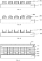
- FIG. 1 is a schematic view of a semiconductor structure in an embodiment of the present disclosure.
- a substrate 100 is provided, and conductive structures 200 arranged at intervals are formed on the surface of the substrate 100.
- the material of the semiconductor substrate 100 is mostly a printed circuit board.
- aluminum nitride substrates, aluminum silicon carbide substrates and the like may be used.
- Conductive structures 200 arranged at intervals are formed on the surface of the substrate 100.
- the conductive structures200 may be pads or traces.
- the material of the conductive structures 200 comprises at least one of copper, nickel, gold, tantalum, cobalt, indium, vanadium, and titanium nitride.
- the gap between the conductive structures 200 and the semiconductor substrate 100 is filled with molding compound 500.
- the molding compound 500 is injected after soldering. In other words, if the soldering is not strong enough, poor contact may occur at the solder joints during the subsequent molding by injection of molding compound 500, or the high-temperature molding may lead to the fusion of the solder, resulting in coupling between adjacent structures and short circuit.
- FIG. 4 shows this embodiment and FIG. 5 shows a technical solution in the prior art.
- the metal solder is generally tin alloy.
- the metal welding material is the fusible portion 400 in FIG. 4 and FIG. 5 .
- the fusible portion 400 is located at the top of the interconnect structures 201 on the chip 110, and is used to bond the fusible portion 400 and the conductive structures 200 by thermocompression to form a package of the chip 110 and the substrate 100. Further, since the conductive structures 200 are relatively infusible at the fusion temperature of the fusible portion 400, the materials of the fusible portion 400 and the conductive structures 200 are different.
- Patterning the conductive structures 200 specifically comprises the following steps.
- a first mask material layer 300 is deposited on the surface of the conductive structures 200 for etching. Further, referring to FIG. 3 , the conductive structures 200 are patterned and etched so that the edges of the conductive structures 200 have protrusions.
- a first mask material layer 300 is formed above the conductive structures 200, and the first mask material layer 300 exposes the edges of the conductive structures.
- a barrier material layer (not shown) is deposited in the first mask material layer 300. The first mask material layer 300 is removed to form protrusions at the edges of the conductive structures.
- the materials of the barrier material layer (not shown) and the conductive structures 200 may be the same or different.
- the material of the barrier material layer may be at least one of metals such as nickel, gold, tantalum, cobalt, indium, titanium nitride, vanadium, and may be a dielectric material with good wettability with the conductive structures 200.
- a second mask material layer (not shown) is formed above the conductive structures 200, the second mask material layer covering at least the edge portion of the conductive structures 200.
- the conductive structures 200 are etched along the second mask material layer to form protrusions at the edges of the conductive structures 200.
- the mask layer there are various methods for depositing the mask layer.
- chemical vapor deposition may be used, in which gases of one or more substances are activated somehow to have chemical reactions on the surface of the substrate and then deposited into a desired solid thin film.
- Physical vapor deposition may be used, in which the transfer of substances is realized by a certain physical process, that is, atoms or molecules are transferred to the surface of the silicon substrate and deposited into a thin film. Spin coating, electroplating and the like may also be used.
- a mask layer with a predetermined thickness is deposited on the surface of the conductive structures 200 by chemical vapor deposition.
- Controlling the flow rate of the introduced airflow, controlling the flow of the introduced airflow, controlling the deposition time, or controlling the deposition temperature may be used separately. By improving the accuracy in controlling the airflow and temperature, all atoms can be deposited neatly to form a single crystalline layer. Finally, a mask layer with a uniform thickness is obtained on the surface of the conductive structures 200.
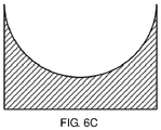
- the deposition and etching of the plurality of mask layers can enable the conductive structures 200 to be etched with a better effect. Meanwhile, a pattern is formed on the mask layer, and the conductive structures 200 are patterned and etched according to the pattern. According to the actual process requirements, for example, referring to the schematic cross-sectional views of the etched conductive structures 200 in FIGS. 6A-6C , a curved groove is formed in the central portion of the conductive structures 200, and protrusions are formed at the edges of the conductive structures 200.
- the etched conductive structures 200 have protrusions on their two edges and the protrusions are one of rectangular, triangular, or curved. Therefore, the pattern of the mask layer may be set to a rectangle, a circle, or the like.
- the conductive structures 200 are patterned and etched so that the edges of the conductive structures 200 have protrusions.
- etching processes for the manufacturing of semiconductors dry etching and wet etching. Dry etching is a process in which the plasmas generated in the gaseous state physically and chemically react with the silicon wafer exposed to the plasmas, through a masking window formed by a photolithography process, to etch away the exposed surface material on the silicon wafer. Dry etching is used in fine etching of small feature sizes in advanced circuits. Dry etching is an etching technique that uses gas as the main medium.
- the semiconductor material does not require liquid chemicals or washing, and the semiconductor material enters and exits the system in a dry state.
- dry etching shows both chemical isotropy (etching in both vertical and horizontal directions) and physical anisotropy (etching only in the vertical direction).
- the conductive structure 200 may be etched by dry etching. Specifically, the semiconductor structure is conveyed to the reaction chamber, and the pressure in the reaction chamber is decreased by a vacuum system. When the reaction chamber is in vacuum, a reaction gas is introduced into the reaction chamber. For the etching of related conductive materials of integrated circuits such as tungsten and copper, a mixture of nitrogen fluoride and oxygen is usually used as the reaction gas. Alternatively, other fluorine-containing gases may be used as the etching gas, for example carbon tetrafluoride, sulfur hexafluoride, and nitrogen trifluoride.
- the power supply creates a radio frequency electric field through the electrodes in the reaction chamber. The energy field excites the mixed gas into the plasma state. In the excited state, the etching is performed with the reactive fluorine and the reactive fluorine is converted into volatile components to be discharged by the vacuum system.
- FIGS. 6A-6C are schematic cross-section views of the etched conductive structures 200.
- FIG. 6A shows rectangular protrusions at the two edges of the etched conductive structures 200
- FIG. 6B shows triangular protrusions at the two edges of the etched conductive structures 200
- FIG. 6C shows curved protrusions at the two edges of the etched conductive structures 200.
- the corresponding effect can be obtained by etching according to the pattern set on the mask layer.
- the shape of the protrusions formed by the first mask material layer 300 is as shown in FIG. 6A .
- Other structures may be obtained by changing the shape of the mask, or by forming the shape of FIG. 6A first and then treating by other processes such as oblique ion implantation and then etching.
- the above other structures may be, for example, protrusions in the shape of FIG. 6B or 6C .
- the deposition and etching of the plurality of mask layers can enable the conductive structures 200 to be etched with a better effect.
- the height of the protrusions is at least greater than or equal to one third of that of the fusible portion 400.
- the edges of the conductive structures 200 have two or more protrusions, and there is a gap between the protrusions. Therefore, sufficient binding force and drainage capacity can be ensured.
- the present disclosure is mainly aimed at improving the conductive structures of the substrate.
- the conductive structures are re-etched. By etching the central portion of the conductive structures, there is a difference in height between the edge and the center.
- the new structure design can drain the metal solder. This can avoid the diffusion of the metal solder along the coupling direction in the subsequent packaging technology, avoid the contact between the metal solder and the surrounding materials, and prevent the metal solder from melting and then flowing to the surrounding during the subsequent high-temperature heating. Thus, this avoids the short circuit between adjacent conductive structures, the current leakage and poor contact between the substrate and the chip, and the product failure. Meanwhile, the metal solder and the conductive structures are welded on three sides to further strengthen the bonding force between the weld metals, thereby improving the yield rate of the semiconductor packaging process.
- a chip 110 is provided, and interconnect structures201 are formed on the surface of the chip 110.
- the chip 100 and the substrate 100 are combined.
- the etched conductive structures 200 are formed on the surface of the substrate 100. Further, the etched conductive structures 200, the interconnect structures 201, and the chip 110 are packaged.
- interconnect structures 201 are formed on the surface of the chip 110, and the top of the interconnect structures 201 has an exposed fusible portion 400.
- the fusible portion 400 is defined to distinguish it from the conductive structures 200.
- the fusible portion 400 is metal solder, generally tin alloy or the like. Since the conductive structures 200 are relatively infusible at the fusion temperature of the fusible portion 400, the materials of the fusible portion 400 and the conductive structures 200 are different.
- the fusible portion 400 and the conductive structures 200 are initially mechanically combined, and then the fusible portion 400 is heated to the reflow temperature of the fusible portion 400 to bond the fusible portion 400 with the conductive structures 200 by thermocompression.
- FIG. 4 shows this embodiment
- FIG. 5 shows a technical solution in the prior art. It may be understood by those skilled in the art that, in the early semiconductor packaging technology, the gap between the conductive structures 200 and the semiconductor substrate 100 is filled with molding compound 500. Due to the fallibility or compactness of the molding compound, when the conductive structures 200 are welded with the interconnect structures 201 on the chip, current leakage, short circuit due to poor contact, product failure and other problems occur between adjacent metal welding materials.
- this embodiment is mainly aimed at improving the conductive structures of the substrate.
- the conductive structures are re-etched. By etching the central portion of the conductive structures, there is a difference in height between the edge and the center.
- the new structure design can drain the metal solder. This can avoid the disordered diffusion of the metal solder in the subsequent packaging technology, and thus avoid the short circuit between adjacent conductive structures.
- the metal solder and the conductive structures are welded on three sides to further strengthen the bonding force between the weld metals. This avoids the current leakage, poor contact and other problems between the substrate and the chip, thereby improving the yield rate of the semiconductor packaging process.
- FIG. 4 is a schematic diagram of a semiconductor structure in other embodiments of the present disclosure.
- the semiconductor structure specifically comprises a substrate 100 and conductive structures 200.
- Conductive structures 200 arranged at intervals are formed on the surface of the substrate 100.
- the conductive structures 200 are located on the surface of the substrate 100. Further, after the conductive structures 200 are etched, the center of the surface is dented and the edges are protruded. Further, the height of the protrusions is at least greater than or equal to one third of that of the fusible portion 400.
- the edges of the conductive structures 200 have two or more protrusions, and there is a gap between the protrusions. Therefore, sufficient binding force and drainage capacity can be ensured.
- the material of the semiconductor substrate 100 is mostly a printed circuit board.
- the material of the semiconductor substrate 100 is mostly a printed circuit board.
- aluminum nitride substrates, aluminum silicon carbide substrates and the like may be used.
- Conductive structures 200 arranged at intervals are formed on the surface of the substrate 100.
- the conductive structures 200 may be pads or traces.
- the material of the conductive structures 200 comprises at least one of copper, nickel, gold, tantalum, cobalt, indium, vanadium, and titanium nitride.
- the protrusions at the two edges of the etched conductive structures 200 are rectangular, triangular, or curved.
- FIG. 6A shows rectangular protrusions at the two edges of the etched conductive structures 200;
- FIG. 6B shows triangular protrusions at the two edges of the etched conductive structures 200;
- FIG. 6C shows curved protrusions at the two edges of the etched conductive structures 200. Therefore, the corresponding effect can be obtained by etching according to the pattern set on the mask layer.
- the shape of the protrusions formed by the first mask material layer 300 is as shown in FIG. 6A .
- Other structures may be obtained by changing the shape of the mask, or by forming the shape of FIG. 6A first and then treating by other processes such as oblique ion implantation and then etching.
- the above other structures may be, for example, protrusions in the shape of FIG. 6B or 6C .
- a chip 110 is provided and interconnect structures 201 are formed on the surface of the chip 110.
- the chip 100 and the substrate 100 are combined.
- the etched conductive structure 200 is formed on the surface of the substrate 100. Further, the etched conductive structure 200, the interconnect structures 201, and the chip 110 are packaged.
- interconnect structures 201 are formed on the surface of the chip 110, and the top of the interconnect structures 201 has an exposed fusible portion 400.
- the fusible portion 400 is defined to distinguish it from the conductive structures 200.
- the fusible portion 400 is metal solder, generally tin alloy. Since the conductive structures 200 are relatively infusible at the fusion temperature of the fusible portion 400, the materials of the fusible portion 400 and the conductive structures 200 are different.
- the fusible portion 400 and the conductive structures 200 are initially mechanically combined, and then the fusible portion 400 is heated to the reflow temperature of the fusible portion 400 to bond the fusible portion 400 with the conductive structures 200 by thermocompression.
- FIG. 4 shows this embodiment
- FIG. 5 shows a technical solution in the prior art.
- the gap between the conductive structures 200 and the semiconductor substrate 100 is filled with molding compound 500.
- the molding compound 500 is injected after soldering.
- the soldering is not strong enough, poor contact may occur at the solder joints during the subsequent molding by injection of molding compound 500, or the high-temperature molding may lead to the fusion of the solder, resulting in coupling between adjacent structures and short circuit. Therefore, due to the fallibility or compactness of the materials, current leakage, poor contact, short circuit and other problems may occur between adjacent metal welding materials, resulting in product failure.
- this embodiment is mainly aimed at improving the conductive structures of the substrate.
- the conductive structures are re-etched. By etching the central portion of the conductive structures, there is a difference in height between the edge and the center.
- the new structure design can drain the metal solder. This can avoid the disordered diffusion of the metal solder in the subsequent packaging technology, and thus avoid the short circuit between adjacent conductive structures.
- the metal solder and the conductive structures are welded on three sides to further strengthen the bonding force between the weld metals. This avoids the current leakage, poor contact and other problems between the substrate and the chip, thereby improving the yield rate of the semiconductor packaging process.
Landscapes
- Internal Circuitry In Semiconductor Integrated Circuit Devices (AREA)
- Engineering & Computer Science (AREA)
- Ceramic Engineering (AREA)
- Physics & Mathematics (AREA)
- Geometry (AREA)
Abstract
Description
- The present disclosure claims the priority to
Chinese Patent Application 202010279542.2, titled "SEMICONDUCTOR STRUCTURES AND METHODS FOR FORMING THE SAME", filed on April 10, 2020 - The present disclosure relates to the field of semiconductor packaging technology, and in particular to a semiconductor structure and a method for forming the same.
- Dynamic random access memory is a semiconductor memory device widely used in semiconductor memories. As the feature size of semiconductor integrated circuit devices is getting smaller, higher requirements on the semiconductor manufacturing technology are proposed. The existing semiconductor packaging technology is limited. Advanced processed are required to enhance the company's competitiveness.
- In the prior art, the gap between the conductive bump and the semiconductor substrate is filled with molding compound. Due to the fallibility or compactness of the molding compound, and the wettability of the solder used in the metal interconnect structures of the chip and the substrate, the welding effect is poor, which in turn leads to product failure in the subsequent molding stage.
- Therefore, in the packaging process of semiconductors with reduced feature size, how to avoid product failure of the chip and semiconductor substrate in the subsequent molding stage and also strengthen the weld metal bonding force between the conductive structures and the substrate is a technical problem to be urgently solved.
- The purpose of the present disclosure is to provide a semiconductor structure and a method for forming the same, which can avoid the product failure of the chip and the semiconductor substrate in the subsequent molding stage, and also strengthen the weld metal bonding force between the conductive structures and the substrate.
- In order to solve the above-mentioned problem, technical solutions proposed as described herein may provide a semiconductor structure formation method including: providing a chip, the chip having interconnect structures on its surface, a top of the interconnect structure having an exposed fusible portion; providing a substrate, the substrate having conductive structures on its surface;
patterning the conductive structures so that edges of the conductive structures have protrusions; combining the chip with the substrate so that the fusible portion and the conductive structure are initially mechanically bonded, and then heating the fusible portion to a reflow temperature of the fusible portion to bond the fusible portion with the conductive structure by thermocompression. - In some embodiments, the patterning the conductive structures comprises: forming a first mask material layer on the conductive structures, the first mask material layer exposing the edges of the conductive structures; depositing a barrier material layer in the first mask material layer; and removing the first mask material layer and forming the protrusions at the edges of the conductive structures.
- In some embodiments, the step of patterning the conductive structures comprises: forming a second mask material layer on the conductive structures, the second mask material layer covering at least edge portions of the conductive structures; and etching the conductive structures along the second mask material layer and forming the protrusions at the edges of the conductive structures.
- In some embodiments, the barrier material layer and the conductive structures are made of the same or different materials.
- The technical solution of the present disclosure further provides a semiconductor structure, comprising:
- a substrate having conductive structures on its surface, the edges of the conductive structures having protrusions; and
- a chip having interconnect structures on its surface, the interconnect structures and the conductive structures fitting with each other face to face.
- In some embodiments, a central portion of the conductive structure has a curved groove, and a top surface of the interconnect structure at least partially fits with the curved groove.
- In some embodiments, the edges of the conductive structures have protrusions and the protrusions are rectangular, triangular, or curved.
- In some embodiments, a top of the interconnect structures has a fusible portion that fits with the conductive structure face to face.
- In some embodiments, the conductive structures and the fusible portion are made of different materials.
- In some embodiments, a height of the protrusion is at least greater than or equal to one third of a height of the fusible portion.
- In some embodiments, the edge of the conductive structure has two or more protrusions, and there is a gap between each protrusion.
- The advantage of the present disclosure is that, compared with the existing semiconductor packaging process, the present disclosure is mainly aimed at improving the conductive structures of the substrate. The new structure design can drain the metal solder, thereby avoiding the diffusion of the metal solder along the pattern direction in the subsequent packaging technology, and also avoiding current leakage, short circuit due to poor contact, product failure and other problems between the conductive structures and the semiconductor substrate. Meanwhile, the metal solder and the conductive structures are welded on three sides to further strengthen the bonding force between the weld metals, thereby improving the yield rate of the semiconductor packaging process.
- In order to explain technical solutions of embodiments of the present disclosure more clearly, the accompanying drawings to be used for describing the embodiments of the present disclosure will be introduced simply. Apparently, the accompanying drawings to be described below are merely some embodiments of the present disclosure. A person of ordinary skill in the art may obtain other drawings according to these drawings without paying any creative effort.
-
FIGS. 1-4 are schematic views of a semiconductor structure in an embodiment of the present disclosure; -
FIG. 5 is a schematic view of a semiconductor structure in the prior art; and -
FIGS. 6A-6C are schematic cross-section views of a semiconductor structure in an embodiment of the present disclosure, - in which:
100: semiconductor substrate; 200: conductive structure; 300: first mask material layer; 400: fusible portion; 201: interconnect structure; 110: chip; 500: molding compound. - In order to make the purposes, technical solutions and effects of the present disclosure clearer, the present disclosure will be further elaborated below with reference to the accompanying drawings. It should be understood that the embodiments to be described here are just some embodiments of the present disclosure, rather than all of the embodiments, and are not intended to limit the present disclosure. Based on the embodiments of the present disclosure, all other embodiments obtained by a person of ordinary skill in the art without paying any creative effort should be included in the protection scope of the present disclosure.
-
FIG. 1 is a schematic view of a semiconductor structure in an embodiment of the present disclosure. - Specifically, a
substrate 100 is provided, andconductive structures 200 arranged at intervals are formed on the surface of thesubstrate 100. - In the semiconductor packaging technology, the material of the
semiconductor substrate 100 is mostly a printed circuit board. For example, aluminum nitride substrates, aluminum silicon carbide substrates and the like may be used.Conductive structures 200 arranged at intervals are formed on the surface of thesubstrate 100. In this embodiment, the conductive structures200 may be pads or traces. In the semiconductor packaging technology, the material of theconductive structures 200 comprises at least one of copper, nickel, gold, tantalum, cobalt, indium, vanadium, and titanium nitride. - It may be understood by those skilled in the art that, in the semiconductor packaging technology, the gap between the
conductive structures 200 and thesemiconductor substrate 100 is filled withmolding compound 500. Themolding compound 500 is injected after soldering. In other words, if the soldering is not strong enough, poor contact may occur at the solder joints during the subsequent molding by injection ofmolding compound 500, or the high-temperature molding may lead to the fusion of the solder, resulting in coupling between adjacent structures and short circuit. - Please referring to
FIG. 4 andFIG. 5 ,FIG. 4 shows this embodiment andFIG. 5 shows a technical solution in the prior art. The metal solder is generally tin alloy. The metal welding material is thefusible portion 400 inFIG. 4 andFIG. 5 . Thefusible portion 400 is located at the top of theinterconnect structures 201 on thechip 110, and is used to bond thefusible portion 400 and theconductive structures 200 by thermocompression to form a package of thechip 110 and thesubstrate 100. Further, since theconductive structures 200 are relatively infusible at the fusion temperature of thefusible portion 400, the materials of thefusible portion 400 and theconductive structures 200 are different. - Patterning the
conductive structures 200 specifically comprises the following steps. - Please referring to
FIG. 2 , a firstmask material layer 300 is deposited on the surface of theconductive structures 200 for etching. Further, referring toFIG. 3 , theconductive structures 200 are patterned and etched so that the edges of theconductive structures 200 have protrusions. - A first
mask material layer 300 is formed above theconductive structures 200, and the firstmask material layer 300 exposes the edges of the conductive structures. A barrier material layer (not shown) is deposited in the firstmask material layer 300. The firstmask material layer 300 is removed to form protrusions at the edges of the conductive structures. The materials of the barrier material layer (not shown) and theconductive structures 200 may be the same or different. The material of the barrier material layer may be at least one of metals such as nickel, gold, tantalum, cobalt, indium, titanium nitride, vanadium, and may be a dielectric material with good wettability with theconductive structures 200. - Further, a second mask material layer (not shown) is formed above the
conductive structures 200, the second mask material layer covering at least the edge portion of theconductive structures 200. Theconductive structures 200 are etched along the second mask material layer to form protrusions at the edges of theconductive structures 200. - Specifically, in this embodiment, there are various methods for depositing the mask layer. For example, chemical vapor deposition may be used, in which gases of one or more substances are activated somehow to have chemical reactions on the surface of the substrate and then deposited into a desired solid thin film. Physical vapor deposition may be used, in which the transfer of substances is realized by a certain physical process, that is, atoms or molecules are transferred to the surface of the silicon substrate and deposited into a thin film. Spin coating, electroplating and the like may also be used. For example, in this embodiment, a mask layer with a predetermined thickness is deposited on the surface of the
conductive structures 200 by chemical vapor deposition. Controlling the flow rate of the introduced airflow, controlling the flow of the introduced airflow, controlling the deposition time, or controlling the deposition temperature may be used separately. By improving the accuracy in controlling the airflow and temperature, all atoms can be deposited neatly to form a single crystalline layer. Finally, a mask layer with a uniform thickness is obtained on the surface of theconductive structures 200. - The deposition and etching of the plurality of mask layers can enable the
conductive structures 200 to be etched with a better effect. Meanwhile, a pattern is formed on the mask layer, and theconductive structures 200 are patterned and etched according to the pattern. According to the actual process requirements, for example, referring to the schematic cross-sectional views of the etchedconductive structures 200 inFIGS. 6A-6C , a curved groove is formed in the central portion of theconductive structures 200, and protrusions are formed at the edges of theconductive structures 200. The etchedconductive structures 200 have protrusions on their two edges and the protrusions are one of rectangular, triangular, or curved. Therefore, the pattern of the mask layer may be set to a rectangle, a circle, or the like. - According to the pattern set on the first
mask material layer 300 in the above steps, theconductive structures 200 are patterned and etched so that the edges of theconductive structures 200 have protrusions. There are two basic etching processes for the manufacturing of semiconductors: dry etching and wet etching. Dry etching is a process in which the plasmas generated in the gaseous state physically and chemically react with the silicon wafer exposed to the plasmas, through a masking window formed by a photolithography process, to etch away the exposed surface material on the silicon wafer. Dry etching is used in fine etching of small feature sizes in advanced circuits. Dry etching is an etching technique that uses gas as the main medium. The semiconductor material does not require liquid chemicals or washing, and the semiconductor material enters and exits the system in a dry state. Compared with wet etching, dry etching shows both chemical isotropy (etching in both vertical and horizontal directions) and physical anisotropy (etching only in the vertical direction). - In this embodiment, the
conductive structure 200 may be etched by dry etching. Specifically, the semiconductor structure is conveyed to the reaction chamber, and the pressure in the reaction chamber is decreased by a vacuum system. When the reaction chamber is in vacuum, a reaction gas is introduced into the reaction chamber. For the etching of related conductive materials of integrated circuits such as tungsten and copper, a mixture of nitrogen fluoride and oxygen is usually used as the reaction gas. Alternatively, other fluorine-containing gases may be used as the etching gas, for example carbon tetrafluoride, sulfur hexafluoride, and nitrogen trifluoride. The power supply creates a radio frequency electric field through the electrodes in the reaction chamber. The energy field excites the mixed gas into the plasma state. In the excited state, the etching is performed with the reactive fluorine and the reactive fluorine is converted into volatile components to be discharged by the vacuum system. - In the semiconductor packaging technology, according to actual process requirements, a curved groove is formed in the central portion of the
conductive structures 200, and the top surface of theinterconnect structures 201 is at least partially engaged with the curved groove. The etchedconductive structures 200 have protrusions on its two edges and the protrusions are rectangular, triangular, or curved.FIGS. 6A-6C are schematic cross-section views of the etchedconductive structures 200. For example,FIG. 6A shows rectangular protrusions at the two edges of the etchedconductive structures 200;FIG. 6B shows triangular protrusions at the two edges of the etchedconductive structures 200; andFIG. 6C shows curved protrusions at the two edges of the etchedconductive structures 200. Therefore, the corresponding effect can be obtained by etching according to the pattern set on the mask layer. Further, in practice, generally, the shape of the protrusions formed by the firstmask material layer 300 is as shown inFIG. 6A . Other structures may be obtained by changing the shape of the mask, or by forming the shape ofFIG. 6A first and then treating by other processes such as oblique ion implantation and then etching. The above other structures may be, for example, protrusions in the shape ofFIG. 6B or6C . Meanwhile, the deposition and etching of the plurality of mask layers can enable theconductive structures 200 to be etched with a better effect. - In some embodiments, the height of the protrusions is at least greater than or equal to one third of that of the
fusible portion 400. The edges of theconductive structures 200 have two or more protrusions, and there is a gap between the protrusions. Therefore, sufficient binding force and drainage capacity can be ensured. - Therefore, in this embodiment, compared with other semiconductor packaging processes, the present disclosure is mainly aimed at improving the conductive structures of the substrate. In the new structure design, equivalently, the conductive structures are re-etched. By etching the central portion of the conductive structures, there is a difference in height between the edge and the center. The new structure design can drain the metal solder. This can avoid the diffusion of the metal solder along the coupling direction in the subsequent packaging technology, avoid the contact between the metal solder and the surrounding materials, and prevent the metal solder from melting and then flowing to the surrounding during the subsequent high-temperature heating. Thus, this avoids the short circuit between adjacent conductive structures, the current leakage and poor contact between the substrate and the chip, and the product failure. Meanwhile, the metal solder and the conductive structures are welded on three sides to further strengthen the bonding force between the weld metals, thereby improving the yield rate of the semiconductor packaging process.
- Please referring to
FIG. 4 , achip 110 is provided, and interconnect structures201 are formed on the surface of thechip 110. Thechip 100 and thesubstrate 100 are combined. The etchedconductive structures 200 are formed on the surface of thesubstrate 100. Further, the etchedconductive structures 200, theinterconnect structures 201, and thechip 110 are packaged. - Specifically,
interconnect structures 201 are formed on the surface of thechip 110, and the top of theinterconnect structures 201 has an exposedfusible portion 400. In this embodiment, thefusible portion 400 is defined to distinguish it from theconductive structures 200. Thefusible portion 400 is metal solder, generally tin alloy or the like. Since theconductive structures 200 are relatively infusible at the fusion temperature of thefusible portion 400, the materials of thefusible portion 400 and theconductive structures 200 are different. - The
fusible portion 400 and theconductive structures 200 are initially mechanically combined, and then thefusible portion 400 is heated to the reflow temperature of thefusible portion 400 to bond thefusible portion 400 with theconductive structures 200 by thermocompression. - Please referring to
FIG. 4 andFIG. 5 ,FIG. 4 shows this embodiment andFIG. 5 shows a technical solution in the prior art. It may be understood by those skilled in the art that, in the early semiconductor packaging technology, the gap between theconductive structures 200 and thesemiconductor substrate 100 is filled withmolding compound 500. Due to the fallibility or compactness of the molding compound, when theconductive structures 200 are welded with theinterconnect structures 201 on the chip, current leakage, short circuit due to poor contact, product failure and other problems occur between adjacent metal welding materials. - Therefore, compared with other semiconductor packaging processes, this embodiment is mainly aimed at improving the conductive structures of the substrate. In the new structure design, equivalently, the conductive structures are re-etched. By etching the central portion of the conductive structures, there is a difference in height between the edge and the center. The new structure design can drain the metal solder. This can avoid the disordered diffusion of the metal solder in the subsequent packaging technology, and thus avoid the short circuit between adjacent conductive structures. Meanwhile, the metal solder and the conductive structures are welded on three sides to further strengthen the bonding force between the weld metals. This avoids the current leakage, poor contact and other problems between the substrate and the chip, thereby improving the yield rate of the semiconductor packaging process.
- In other embodiments of the present disclosure provides a semiconductor structure.
-
FIG. 4 is a schematic diagram of a semiconductor structure in other embodiments of the present disclosure. - The semiconductor structure specifically comprises a
substrate 100 andconductive structures 200. -
Conductive structures 200 arranged at intervals are formed on the surface of thesubstrate 100. Theconductive structures 200 are located on the surface of thesubstrate 100. Further, after theconductive structures 200 are etched, the center of the surface is dented and the edges are protruded. Further, the height of the protrusions is at least greater than or equal to one third of that of thefusible portion 400. The edges of theconductive structures 200 have two or more protrusions, and there is a gap between the protrusions. Therefore, sufficient binding force and drainage capacity can be ensured. - Specifically, in the semiconductor packaging technology, the material of the
semiconductor substrate 100 is mostly a printed circuit board. For example, aluminum nitride substrates, aluminum silicon carbide substrates and the like may be used.Conductive structures 200 arranged at intervals are formed on the surface of thesubstrate 100. In this embodiment, theconductive structures 200 may be pads or traces. In the semiconductor packaging technology, the material of theconductive structures 200 comprises at least one of copper, nickel, gold, tantalum, cobalt, indium, vanadium, and titanium nitride. - According to actual process requirements, referring to the schematic views of the etched
conductive structures 200 inFIGS. 6A-6C , for example, the protrusions at the two edges of the etchedconductive structures 200 are rectangular, triangular, or curved.FIG. 6A shows rectangular protrusions at the two edges of the etchedconductive structures 200;FIG. 6B shows triangular protrusions at the two edges of the etchedconductive structures 200; andFIG. 6C shows curved protrusions at the two edges of the etchedconductive structures 200. Therefore, the corresponding effect can be obtained by etching according to the pattern set on the mask layer. Further, in practice, generally, the shape of the protrusions formed by the firstmask material layer 300 is as shown inFIG. 6A . Other structures may be obtained by changing the shape of the mask, or by forming the shape ofFIG. 6A first and then treating by other processes such as oblique ion implantation and then etching. The above other structures may be, for example, protrusions in the shape ofFIG. 6B or6C . - A
chip 110 is provided andinterconnect structures 201 are formed on the surface of thechip 110. Thechip 100 and thesubstrate 100 are combined. The etchedconductive structure 200 is formed on the surface of thesubstrate 100. Further, the etchedconductive structure 200, theinterconnect structures 201, and thechip 110 are packaged. - Specifically,
interconnect structures 201 are formed on the surface of thechip 110, and the top of theinterconnect structures 201 has an exposedfusible portion 400. In this embodiment, thefusible portion 400 is defined to distinguish it from theconductive structures 200. Thefusible portion 400 is metal solder, generally tin alloy. Since theconductive structures 200 are relatively infusible at the fusion temperature of thefusible portion 400, the materials of thefusible portion 400 and theconductive structures 200 are different. - The
fusible portion 400 and theconductive structures 200 are initially mechanically combined, and then thefusible portion 400 is heated to the reflow temperature of thefusible portion 400 to bond thefusible portion 400 with theconductive structures 200 by thermocompression. - Please referring to
FIG. 4 andFIG. 5 ,FIG. 4 shows this embodiment andFIG. 5 shows a technical solution in the prior art. - It may be understood by those skilled in the art that, in the semiconductor packaging technology, the gap between the
conductive structures 200 and thesemiconductor substrate 100 is filled withmolding compound 500. Themolding compound 500 is injected after soldering. In other words, if the soldering is not strong enough, poor contact may occur at the solder joints during the subsequent molding by injection ofmolding compound 500, or the high-temperature molding may lead to the fusion of the solder, resulting in coupling between adjacent structures and short circuit. Therefore, due to the fallibility or compactness of the materials, current leakage, poor contact, short circuit and other problems may occur between adjacent metal welding materials, resulting in product failure. - Therefore, compared with other semiconductor packaging processes, this embodiment is mainly aimed at improving the conductive structures of the substrate. In the new structure design, equivalently, the conductive structures are re-etched. By etching the central portion of the conductive structures, there is a difference in height between the edge and the center. The new structure design can drain the metal solder. This can avoid the disordered diffusion of the metal solder in the subsequent packaging technology, and thus avoid the short circuit between adjacent conductive structures. Meanwhile, the metal solder and the conductive structures are welded on three sides to further strengthen the bonding force between the weld metals. This avoids the current leakage, poor contact and other problems between the substrate and the chip, thereby improving the yield rate of the semiconductor packaging process.
- The foregoing descriptions are merely preferred embodiments of the present disclosure. It should be noted that, for a person of ordinary skill in the art, various improvements and modifications may be made without departing from the principle of the present disclosure, and these improvements and modifications shall be deemed as falling into the protection scope of the present disclosure.
Claims (10)
- A method for forming a semiconductor structure, comprising:providing a chip, the chip having interconnect structures on its surface, a top of the interconnect structure having an exposed fusible portion;providing a substrate, the substrate having conductive structures on its surface;patterning the conductive structures so that edges of the conductive structures have protrusions;combining the chip with the substrate so that the fusible portion and the conductive structure are initially mechanically bonded, and then heating the fusible portion to a reflow temperature of the fusible portion to bond the fusible portion with the conductive structure by thermocompression.
- The method for forming a semiconductor structure according to claim 1, wherein the patterning the conductive structures comprises: forming a first mask material layer on the conductive structures, the first mask material layer exposing the edges of the conductive structures;depositing a barrier material layer in the first mask material layer; andremoving the first mask material layer and forming the protrusions at the edges of the conductive structures.
- The method for forming a semiconductor structure according to claim 1, wherein the patterning the conductive structures comprises: forming a second mask material layer on the conductive structures, the second mask material layer covering at least edge portions of the conductive structures; and
etching the conductive structures along the second mask material layer and forming the protrusions at the edges of the conductive structures. - The method for forming a semiconductor structure according to claim 2, wherein the barrier material layer and the conductive structures are made of same or different materials.
- A semiconductor structure, comprising:a substrate, having conductive structures on its surface, edges of the conductive structures having protrusions; anda chip, having interconnect structures on its surface, the interconnect structures and the conductive structures fitting with each other face to face.
- The semiconductor structure according to claim 5, wherein a central portion of the conductive structure has a curved groove, and a top surface of the interconnect structure at least partially fits with the curved groove.
- The semiconductor structure according to claim 5, wherein shape of the protrusions is one of rectangular, triangular, or curved.
- The semiconductor structure according to claim 5, wherein a top of the interconnect structure has a fusible portion that fits with the conductive structure face to face.
- The semiconductor structure according to claim 8, wherein a height of the protrusion is at least greater than or equal to one third of a height of the fusible portion.
- The semiconductor structure according to claim 5, wherein the edge of the conductive structure has two or more protrusions, and there is a gap between each protrusion.
Applications Claiming Priority (2)
| Application Number | Priority Date | Filing Date | Title |
|---|---|---|---|
| CN202010279542.2A CN113517209A (en) | 2020-04-10 | 2020-04-10 | Semiconductor structure and method of forming the same |
| PCT/CN2021/079980 WO2021203900A1 (en) | 2020-04-10 | 2021-03-10 | Semiconductor structure and formation method therefor |
Publications (2)
| Publication Number | Publication Date |
|---|---|
| EP3933898A1 true EP3933898A1 (en) | 2022-01-05 |
| EP3933898A4 EP3933898A4 (en) | 2023-08-09 |
Family
ID=78023379
Family Applications (1)
| Application Number | Title | Priority Date | Filing Date |
|---|---|---|---|
| EP21773255.1A Withdrawn EP3933898A4 (en) | 2020-04-10 | 2021-03-10 | SEMICONDUCTOR STRUCTURE AND METHOD FOR FORMING IT |
Country Status (4)
| Country | Link |
|---|---|
| US (1) | US12033933B2 (en) |
| EP (1) | EP3933898A4 (en) |
| CN (1) | CN113517209A (en) |
| WO (1) | WO2021203900A1 (en) |
Families Citing this family (1)
| Publication number | Priority date | Publication date | Assignee | Title |
|---|---|---|---|---|
| CN116759321A (en) * | 2023-08-21 | 2023-09-15 | 广州市艾佛光通科技有限公司 | Semiconductor chip pad and manufacturing method, chip packaging method |
Family Cites Families (14)
| Publication number | Priority date | Publication date | Assignee | Title |
|---|---|---|---|---|
| CN101431037B (en) * | 2007-11-06 | 2011-03-30 | 宏茂微电子(上海)有限公司 | Manufacturing method of wafer level packaging structure |
| US8604624B2 (en) | 2008-03-19 | 2013-12-10 | Stats Chippac Ltd. | Flip chip interconnection system having solder position control mechanism |
| JP5237242B2 (en) * | 2009-11-27 | 2013-07-17 | 日東電工株式会社 | Wiring circuit structure and manufacturing method of semiconductor device using the same |
| US8241963B2 (en) * | 2010-07-13 | 2012-08-14 | Taiwan Semiconductor Manufacturing Company, Ltd. | Recessed pillar structure |
| US9087701B2 (en) * | 2011-04-30 | 2015-07-21 | Stats Chippac, Ltd. | Semiconductor device and method of embedding TSV semiconductor die within substrate for vertical interconnect in POP |
| JPWO2014033977A1 (en) * | 2012-08-29 | 2016-08-08 | パナソニックIpマネジメント株式会社 | Semiconductor device |
| US9117825B2 (en) * | 2012-12-06 | 2015-08-25 | Taiwan Semiconductor Manufacturing Company, Ltd. | Substrate pad structure |
| US20150318259A1 (en) * | 2014-05-02 | 2015-11-05 | KyungOe Kim | Integrated circuit packaging system with no-reflow connection and method of manufacture thereof |
| JP6615701B2 (en) * | 2016-06-24 | 2019-12-04 | 新光電気工業株式会社 | WIRING BOARD, SEMICONDUCTOR DEVICE, AND WIRING BOARD MANUFACTURING METHOD |
| US10390440B1 (en) * | 2018-02-01 | 2019-08-20 | Nxp B.V. | Solderless inter-component joints |
| US20200006273A1 (en) * | 2018-06-28 | 2020-01-02 | Intel Corporation | Microelectronic device interconnect structure |
| JP7516786B2 (en) * | 2019-06-21 | 2024-07-17 | 株式会社村田製作所 | Semiconductor device and its manufacturing method |
| EP3793336A1 (en) * | 2019-09-10 | 2021-03-17 | AT & S Austria Technologie & Systemtechnik Aktiengesellschaft | Connection arrangement, component carrier and method of forming a component carrier structure |
| US11682641B2 (en) * | 2020-08-13 | 2023-06-20 | Microchip Technology Incorporated | Integrated circuit bond pad with multi-material toothed structure |
-
2020
- 2020-04-10 CN CN202010279542.2A patent/CN113517209A/en active Pending
-
2021
- 2021-03-10 EP EP21773255.1A patent/EP3933898A4/en not_active Withdrawn
- 2021-03-10 US US17/432,191 patent/US12033933B2/en active Active
- 2021-03-10 WO PCT/CN2021/079980 patent/WO2021203900A1/en not_active Ceased
Also Published As
| Publication number | Publication date |
|---|---|
| CN113517209A (en) | 2021-10-19 |
| WO2021203900A1 (en) | 2021-10-14 |
| EP3933898A4 (en) | 2023-08-09 |
| US12033933B2 (en) | 2024-07-09 |
| US20230118163A1 (en) | 2023-04-20 |
Similar Documents
| Publication | Publication Date | Title |
|---|---|---|
| US9589879B2 (en) | Substrates with through vias with conductive features for connection to integrated circuit elements, and methods for forming through vias in substrates | |
| CN202352660U (en) | Microelectronic package | |
| US6878633B2 (en) | Flip-chip structure and method for high quality inductors and transformers | |
| KR100708282B1 (en) | Semiconductor device and fabrication method thereof | |
| WO2019221974A1 (en) | Structures for bonding elements | |
| US20050142835A1 (en) | Method of disposing conductive bumps onto a semiconductor device and semiconductor devices so formed | |
| TWI402925B (en) | Metal pillar bump structure and forming method thereof | |
| KR100927120B1 (en) | Semiconductor device packaging method | |
| JP2003203940A (en) | Semiconductor chip, wiring board, and manufacturing method thereof, semiconductor wafer, semiconductor device, circuit board, and electronic equipment | |
| TW201401482A (en) | Stacked package component and method of packaging semiconductor wafer | |
| JP6383791B2 (en) | Wafer dicing method for improving die packaging quality | |
| US20030019917A1 (en) | Bump forming method, presoldering treatment method, soldering method, bump forming apparatus, presoldering treatment device and soldering apparatus | |
| KR102947134B1 (en) | Bumpless superconducting device | |
| US12033933B2 (en) | Semiconductor structures and methods for forming the same | |
| US20140103522A1 (en) | Semiconductor substrate, semiconductor device, and method of manfacturing semiconductor substrate | |
| TW202312374A (en) | Stiffener frame for semiconductor device packages | |
| JP4155154B2 (en) | Semiconductor device, circuit board, and electronic device | |
| CN101521170A (en) | Solder contacts and methods of forming same | |
| TWI593079B (en) | Electronic package and its manufacturing method | |
| US6699780B1 (en) | Method of connecting a conductive trace to a semiconductor chip using plasma undercut etching | |
| JP2008218884A (en) | Semiconductor device and manufacturing method thereof | |
| US9312175B2 (en) | Surface modified TSV structure and methods thereof | |
| US11855032B2 (en) | Semiconductor structure and manufacturing method thereof | |
| CN210467824U (en) | Semiconductor packaging structure | |
| CN121035094A (en) | A semiconductor packaging structure and its fabrication method |
Legal Events
| Date | Code | Title | Description |
|---|---|---|---|
| STAA | Information on the status of an ep patent application or granted ep patent |
Free format text: STATUS: UNKNOWN |
|
| STAA | Information on the status of an ep patent application or granted ep patent |
Free format text: STATUS: THE INTERNATIONAL PUBLICATION HAS BEEN MADE |
|
| PUAI | Public reference made under article 153(3) epc to a published international application that has entered the european phase |
Free format text: ORIGINAL CODE: 0009012 |
|
| STAA | Information on the status of an ep patent application or granted ep patent |
Free format text: STATUS: REQUEST FOR EXAMINATION WAS MADE |
|
| 17P | Request for examination filed |
Effective date: 20210929 |
|
| AK | Designated contracting states |
Kind code of ref document: A1 Designated state(s): AL AT BE BG CH CY CZ DE DK EE ES FI FR GB GR HR HU IE IS IT LI LT LU LV MC MK MT NL NO PL PT RO RS SE SI SK SM TR |
|
| DAV | Request for validation of the european patent (deleted) | ||
| DAX | Request for extension of the european patent (deleted) | ||
| A4 | Supplementary search report drawn up and despatched |
Effective date: 20230710 |
|
| RIC1 | Information provided on ipc code assigned before grant |
Ipc: H01L 23/00 20060101ALI20230704BHEP Ipc: H01L 21/603 20060101AFI20230704BHEP |
|
| STAA | Information on the status of an ep patent application or granted ep patent |
Free format text: STATUS: THE APPLICATION HAS BEEN WITHDRAWN |
|
| 18W | Application withdrawn |
Effective date: 20231208 |