EP3929997B1 - Anzeigevorrichtung und verfahren zur bereitstellung davon - Google Patents
Anzeigevorrichtung und verfahren zur bereitstellung davon Download PDFInfo
- Publication number
- EP3929997B1 EP3929997B1 EP21180605.4A EP21180605A EP3929997B1 EP 3929997 B1 EP3929997 B1 EP 3929997B1 EP 21180605 A EP21180605 A EP 21180605A EP 3929997 B1 EP3929997 B1 EP 3929997B1
- Authority
- EP
- European Patent Office
- Prior art keywords
- layer
- color
- light
- sub
- light emitting
- Prior art date
- Legal status (The legal status is an assumption and is not a legal conclusion. Google has not performed a legal analysis and makes no representation as to the accuracy of the status listed.)
- Active
Links
Images








Classifications
-
- H—ELECTRICITY
- H10—SEMICONDUCTOR DEVICES; ELECTRIC SOLID-STATE DEVICES NOT OTHERWISE PROVIDED FOR
- H10K—ORGANIC ELECTRIC SOLID-STATE DEVICES
- H10K59/00—Integrated devices, or assemblies of multiple devices, comprising at least one organic light-emitting element covered by group H10K50/00
- H10K59/50—OLEDs integrated with light modulating elements, e.g. with electrochromic elements, photochromic elements or liquid crystal elements
-
- G—PHYSICS
- G02—OPTICS
- G02B—OPTICAL ELEMENTS, SYSTEMS OR APPARATUS
- G02B5/00—Optical elements other than lenses
- G02B5/20—Filters
- G02B5/201—Filters in the form of arrays
-
- G—PHYSICS
- G02—OPTICS
- G02B—OPTICAL ELEMENTS, SYSTEMS OR APPARATUS
- G02B5/00—Optical elements other than lenses
- G02B5/30—Polarising elements
-
- H—ELECTRICITY
- H10—SEMICONDUCTOR DEVICES; ELECTRIC SOLID-STATE DEVICES NOT OTHERWISE PROVIDED FOR
- H10K—ORGANIC ELECTRIC SOLID-STATE DEVICES
- H10K59/00—Integrated devices, or assemblies of multiple devices, comprising at least one organic light-emitting element covered by group H10K50/00
- H10K59/10—OLED displays
- H10K59/12—Active-matrix OLED [AMOLED] displays
- H10K59/121—Active-matrix OLED [AMOLED] displays characterised by the geometry or disposition of pixel elements
-
- H—ELECTRICITY
- H10—SEMICONDUCTOR DEVICES; ELECTRIC SOLID-STATE DEVICES NOT OTHERWISE PROVIDED FOR
- H10K—ORGANIC ELECTRIC SOLID-STATE DEVICES
- H10K59/00—Integrated devices, or assemblies of multiple devices, comprising at least one organic light-emitting element covered by group H10K50/00
- H10K59/10—OLED displays
- H10K59/12—Active-matrix OLED [AMOLED] displays
- H10K59/122—Pixel-defining structures or layers, e.g. banks
-
- H—ELECTRICITY
- H10—SEMICONDUCTOR DEVICES; ELECTRIC SOLID-STATE DEVICES NOT OTHERWISE PROVIDED FOR
- H10K—ORGANIC ELECTRIC SOLID-STATE DEVICES
- H10K59/00—Integrated devices, or assemblies of multiple devices, comprising at least one organic light-emitting element covered by group H10K50/00
- H10K59/10—OLED displays
- H10K59/12—Active-matrix OLED [AMOLED] displays
- H10K59/126—Shielding, e.g. light-blocking means over the TFTs
-
- H—ELECTRICITY
- H10—SEMICONDUCTOR DEVICES; ELECTRIC SOLID-STATE DEVICES NOT OTHERWISE PROVIDED FOR
- H10K—ORGANIC ELECTRIC SOLID-STATE DEVICES
- H10K59/00—Integrated devices, or assemblies of multiple devices, comprising at least one organic light-emitting element covered by group H10K50/00
- H10K59/30—Devices specially adapted for multicolour light emission
- H10K59/35—Devices specially adapted for multicolour light emission comprising red-green-blue [RGB] subpixels
- H10K59/353—Devices specially adapted for multicolour light emission comprising red-green-blue [RGB] subpixels characterised by the geometrical arrangement of the RGB subpixels
-
- H—ELECTRICITY
- H10—SEMICONDUCTOR DEVICES; ELECTRIC SOLID-STATE DEVICES NOT OTHERWISE PROVIDED FOR
- H10K—ORGANIC ELECTRIC SOLID-STATE DEVICES
- H10K59/00—Integrated devices, or assemblies of multiple devices, comprising at least one organic light-emitting element covered by group H10K50/00
- H10K59/30—Devices specially adapted for multicolour light emission
- H10K59/38—Devices specially adapted for multicolour light emission comprising colour filters or colour changing media [CCM]
-
- H—ELECTRICITY
- H10—SEMICONDUCTOR DEVICES; ELECTRIC SOLID-STATE DEVICES NOT OTHERWISE PROVIDED FOR
- H10K—ORGANIC ELECTRIC SOLID-STATE DEVICES
- H10K59/00—Integrated devices, or assemblies of multiple devices, comprising at least one organic light-emitting element covered by group H10K50/00
- H10K59/80—Constructional details
- H10K59/8791—Arrangements for improving contrast, e.g. preventing reflection of ambient light
- H10K59/8792—Arrangements for improving contrast, e.g. preventing reflection of ambient light comprising light absorbing layers, e.g. black layers
-
- H—ELECTRICITY
- H10—SEMICONDUCTOR DEVICES; ELECTRIC SOLID-STATE DEVICES NOT OTHERWISE PROVIDED FOR
- H10K—ORGANIC ELECTRIC SOLID-STATE DEVICES
- H10K71/00—Manufacture or treatment specially adapted for the organic devices covered by this subclass
-
- H—ELECTRICITY
- H10—SEMICONDUCTOR DEVICES; ELECTRIC SOLID-STATE DEVICES NOT OTHERWISE PROVIDED FOR
- H10K—ORGANIC ELECTRIC SOLID-STATE DEVICES
- H10K2102/00—Constructional details relating to the organic devices covered by this subclass
- H10K2102/301—Details of OLEDs
- H10K2102/302—Details of OLEDs of OLED structures
- H10K2102/3023—Direction of light emission
- H10K2102/3026—Top emission
-
- H—ELECTRICITY
- H10—SEMICONDUCTOR DEVICES; ELECTRIC SOLID-STATE DEVICES NOT OTHERWISE PROVIDED FOR
- H10K—ORGANIC ELECTRIC SOLID-STATE DEVICES
- H10K2102/00—Constructional details relating to the organic devices covered by this subclass
- H10K2102/301—Details of OLEDs
- H10K2102/331—Nanoparticles used in non-emissive layers, e.g. in packaging layer
-
- H—ELECTRICITY
- H10—SEMICONDUCTOR DEVICES; ELECTRIC SOLID-STATE DEVICES NOT OTHERWISE PROVIDED FOR
- H10K—ORGANIC ELECTRIC SOLID-STATE DEVICES
- H10K59/00—Integrated devices, or assemblies of multiple devices, comprising at least one organic light-emitting element covered by group H10K50/00
- H10K59/30—Devices specially adapted for multicolour light emission
- H10K59/32—Stacked devices having two or more layers, each emitting at different wavelengths
-
- H—ELECTRICITY
- H10—SEMICONDUCTOR DEVICES; ELECTRIC SOLID-STATE DEVICES NOT OTHERWISE PROVIDED FOR
- H10K—ORGANIC ELECTRIC SOLID-STATE DEVICES
- H10K59/00—Integrated devices, or assemblies of multiple devices, comprising at least one organic light-emitting element covered by group H10K50/00
- H10K59/80—Constructional details
- H10K59/875—Arrangements for extracting light from the devices
- H10K59/877—Arrangements for extracting light from the devices comprising scattering means
-
- H—ELECTRICITY
- H10—SEMICONDUCTOR DEVICES; ELECTRIC SOLID-STATE DEVICES NOT OTHERWISE PROVIDED FOR
- H10K—ORGANIC ELECTRIC SOLID-STATE DEVICES
- H10K59/00—Integrated devices, or assemblies of multiple devices, comprising at least one organic light-emitting element covered by group H10K50/00
- H10K59/80—Constructional details
- H10K59/875—Arrangements for extracting light from the devices
- H10K59/878—Arrangements for extracting light from the devices comprising reflective means
Definitions
- the disclosure relates to a display device and a method of providing the same.
- LCD liquid crystal display
- OLED organic light emitting display
- the display devices include a self-light emitting display device which includes a self-light emitting element such as an organic light emitting diode and excludes a separate power source.
- the self-light emitting element may include two opposing electrodes and a light emitting layer which is interposed therebetween.
- the organic light emitting diode as the self-light emitting element, the electrons and holes from the two electrodes are recombined in the light emitting layer to produce excitons, which transition from the excited state to the ground state, emitting light.
- Such a self-light emitting display device is attracting attention as a next-generation display as meeting the high display quality requirements such as wide viewing angle, high brightness and contrast, and quick response speed, as well as having a low power consumption, a light weight, and a small thickness due to omitting the separate power source.
- EP 3 355 357 A1 discloses a light-emitting display device.
- Embodiments of the invention provide a display device having reduced color mixing between adjacent pixels and/or between adjacent sub-pixels and a method of providing the display device having the reduced color mixing.
- An embodiment of a display device includes a first display substrate including a light emitting element which emits light of a first color or light of a second color different from the first color, a second display substrate including in order toward the first display substrate, a layer including both a bank layer defining an opening and a wavelength control pattern in the opening, a capping layer covering the wavelength control pattern and the bank layer, and a color absorbing layer which corresponds to the bank layer and blocks the light of the first color and the light of the second color.
- the capping layer includes a first area corresponding to the color absorbing layer
- the bank layer includes a second area corresponding to the color absorbing layer
- the first area of the capping layer is between the color absorbing layer and the second area of the bank layer.
- An embodiment of a display device includes a substrate, a light emitting element which faces the substrate and emits blue light and green light; and in order from the substrate to the light emitting element a layer including both a bank layer defining an opening and a wavelength control pattern in the opening, a capping layer covering the wavelength control pattern and the bank layer and a color absorbing layer which corresponds to the bank layer.
- the color absorbing layer blocks both the blue light and the green light which is emitted from the light emitting element, and transmits red light.
- An embodiment of a method of fabricating a display device includes providing a bank layer defining an opening on a substrate, providing a color control layer in the opening, providing a capping layer covering the bank layer and the color control layer, after providing the capping layer, providing a color absorbing material layer on the capping layer, and patterning the color absorbing material layer on the capping layer, to provide a color absorbing pattern corresponding to the bank layer.
- the capping layer includes a first area corresponding to the color absorbing pattern
- the bank layer includes a second area corresponding to the color absorbing pattern
- the first area of the capping layer is between the color absorbing pattern and the second area of the bank layer.
- color mixing between adjacent pixels and/or between adjacent sub-pixels is reduced or effectively prevented.
- first,” “second,” etc. may be used herein to describe various elements, these elements, should not be limited by these terms. These terms may be used to distinguish one element from another element. Thus, a first element discussed below may be termed a second element without departing from teachings of one or more embodiments. The description of an element as a “first” element may not require or imply the presence of a second element or other elements.
- the terms “first,” “second,” etc. may also be used herein to differentiate different categories or sets of elements. For conciseness, the terms “first,” “second,” etc. may represent “first-category (or first-set)", “second-category (or second-set),” etc., respectively.
- relative terms such as “lower” or “bottom” and “upper” or “top,” may be used herein to describe one element's relationship to another element as illustrated in the Figures. It will be understood that relative terms are intended to encompass different orientations of the device in addition to the orientation depicted in the Figures. For example, if the device in one of the figures is turned over, elements described as being on the “lower” side of other elements would then be oriented on “upper” sides of the other elements. The term “lower,” can therefore, encompasses both an orientation of “lower” and “upper,” depending on the particular orientation of the figure.
- Embodiments are described herein with reference to cross section illustrations that are schematic illustrations of idealized embodiments. As such, variations from the shapes of the illustrations as a result, for example, of manufacturing techniques and/or tolerances, are to be expected. Thus, embodiments described herein should not be construed as limited to the particular shapes of regions as illustrated herein but are to include deviations in shapes that result, for example, from manufacturing. For example, a region illustrated or described as flat may, typically, have rough and/or nonlinear features. Moreover, sharp angles that are illustrated may be rounded. Thus, the regions illustrated in the figures are schematic in nature and their shapes are not intended to illustrate the precise shape of a region and are not intended to limit the scope of the claims.
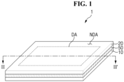
- FIG. 1 is a perspective view of an embodiment of a display device 1.
- a display device 1 may refer to any electronic device providing a display screen at which an image is displayed.
- Examples of the display device 1 may include a television, a laptop computer, a monitor, a billboard, a mobile phone, a smartphone, a tablet personal computer ("PC"), an electronic watch, a smart watch, a watch phone, a mobile communication terminal, an electronic notebook, an electronic book, a portable multimedia player ("PMP"), a navigation device, a game machine, a digital camera, an Internet-of-Things device and the like, which provide a display screen.
- PMP portable multimedia player
- the display device 1 illustrated in the drawing is a television ("TV”).
- the display device 1 may have a high resolution or an ultra-high resolution such as high definition (“HD”), ultra-high definition (“UHD”), 4K and 8K, without being limited thereto.
- HD high definition
- UHD ultra-high definition
- 4K 4K
- 8K 8K
- the display device 1 may have a rectangular shape in a plan view.
- the planar shape of the display device 1 is not limited to the exemplified one, but may have a circular shape or other planar shapes.
- the display device 1 may include a display area DA at which an image is displayed and a non-display area NDA at which an image is not displayed.
- the display area DA may include a pixel PX provided in plural including a plurality of pixels PX at which light is generated, an image is displayed, etc.
- the non-display area NDA is adjacent to the display area DA.
- the non-display area NDA may be located around the display area DA and may surround the display area DA, in the plan view.
- FIG. 2 is a cross-sectional view taken along line II-II' of FIG. 1 .
- the display device 1 may include a first display substrate 10 and a second display substrate 20 facing the first display substrate 10.
- the display device 1 may further include a sealing member 50 that couples the first display substrate 10 to the second display substrate 20, and a filling layer 70 which fills a space between the first display substrate 10 and the second display substrate 20.
- the first display substrate 10 may include elements and circuits for generating and/or displaying an image.
- the first display substrate 10 may include, for example, a pixel circuit such as a switching element, a self-light emitting element, and a pixel defining layer PDL that defines an emission region EMA (e.g., light emission region) and a non-emission region NEM which is adjacent to the emission region EMA, which will be described later, in the display area DA.
- a pixel circuit such as a switching element, a self-light emitting element, and a pixel defining layer PDL that defines an emission region EMA (e.g., light emission region) and a non-emission region NEM which is adjacent to the emission region EMA, which will be described later, in the display area DA.
- EMA e.g., light emission region
- NEM non-emission region
- the self-light emitting element may include at least one of an organic light emitting diode, a quantum dot light emitting diode, an inorganic micro light emitting diode (e.g., micro LED) and an inorganic nano light emitting diode (e.g., nano LED).
- an organic light emitting diode e.g., a quantum dot light emitting diode
- an inorganic micro light emitting diode e.g., micro LED
- an inorganic nano light emitting diode e.g., nano LED
- the second display substrate 20 may be located above the first display substrate 10 to face the first display substrate 10.
- the second display substrate 20 may include a color control structure that converts the color of light incident thereto (e.g., incident light).
- the color control structure may control the wavelength of incident light, thereby converting the color of incident light.
- the sealing member 50 may be positioned between the first display substrate 10 and the second display substrate 20, in the non-display area NDA.
- the sealing member 50 may be disposed along edges of the first display substrate 10 and the second display substrate 20 in the non-display area NDA, and may surround the display area DA in a plan view.
- the first display substrate 10 and the second display substrate 20 may be coupled to each other via the sealing member 50.
- the sealing member 50 may include an organic material.
- the sealing member 50 may include or be made of an epoxy resin, but is not limited thereto.
- a filling layer 70 may be disposed in a space defined between the first display substrate 10 and the second display substrate 20 together with the sealing member 50.
- the filling layer 70 may fill the space between the first display substrate 10 and the second display substrate 20. That is, the filling layer 70 may fill the space between the first display substrate 10 and the second display substrate 20, and may serve to bond the first display substrate 10 and the second display substrate 20 to each other.
- the filling layer 70 may include or be made of a material that can transmit light.
- the filling layer 70 may include an organic material. In an embodiment, for example, the filling layer 70 may include or be formed of a Si-based organic material, an epoxy-based organic material or the like, but is not limited thereto. In an embodiment, the filling layer 70 may be omitted.
- FIG. 3 is a schematic plan view showing an embodiment of a pixel arrangement of a display device 1.
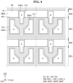
- FIG. 4 is a schematic plan view showing an embodiment of a pixel arrangement relative to an arrangement of a color mixing prevention layer MCL in a display device 1.
- FIG. 4 shows a planar arrangement of an embodiment of a color mixing prevention layer MCL.
- a first direction DR1 indicates a horizontal direction
- a second direction DR2 indicates a vertical direction which intersects the first direction DR1
- a third direction DR3 indicates a thickness direction of the display device 1 (see FIG. 1 ) which intersects both the first direction DR1 and the second direction DR2.
- the display area DA of the display device 1 includes a plurality of pixels PX.
- the pixel PX represents a minimum unit repeated for generation of light, display of an image, etc.
- each pixel PX may include a plurality of sub-pixels PXS emitting different colors.
- each one of the pixels PX may include a first sub-pixel PXS_1 at which red light is emitted from the display device 1 (e.g., red light emission), a second sub-pixel PXS_2 at which green light is emitted from the display device 1 (e.g., green light emission), and a third sub-pixel PXS_3 at which blue light is emitted from the display device 1 (e.g., blue light emission).
- the first sub-pixel PXS_1, the second sub-pixel PXS_2 and the third sub-pixel PXS_3 may be provided in one-to-one correspondence within each of the pixels PX.
- Each of the sub-pixels PXS may include a light transmission region TA and a light blocking region BA which is adjacent to the light transmission region TA.
- the light blocking region BA may be located around the light transmission region TA and may surround the light transmission region TA, in the plan view.
- the light transmission region TA may be a planar area at which light emitted from the emission region EMA is transmitted to the outside of the display device 1 (see FIG. 1 ). In other words, light emitted from the emission region EMA is transmitted to the outside of the display device 1 (see FIG. 1 ) through the light transmission region TA.
- the light blocking region BA may be a planar area at which light emitted from the emission region EMA is not transmitted to the outside of the display device 1 (see FIG. 1 ). In other words, the light blocking region BA may block light emitted from the emission region EMA such that the light is not transmitted to the outside of the display device 1 through the light blocking region BA (see FIG. 1 ).
- the light blocking region BA of one of the sub-pixels PXS is in contact with the light blocking region BA of a neighboring one of the sub-pixels PXS (regardless of whether the light blocking regions BA respectively correspond to sub-pixels PXS in a same one of the pixels PX).
- the light blocking regions BA of the sub-pixels PXS which are adjacent to each other may be integrally connected to each other. Further, the light blocking regions BA of all the sub-pixels PXS may be integrally connected to each other, but is not limited thereto.
- the light transmission regions TA of the sub-pixels PXS which are adjacent to each other may be separated from and distinguished from each other by the light blocking region BA. The light transmission region TA and the light blocking region BA will be described in detail later.
- the light transmission regions TA include a first light transmission region TA1, a second light transmission region TA2 and a third light transmission region TA3 (e.g., light transmission regions TA1, TA2 and TA3).
- the planar shapes of the light transmission regions TA of the sub-pixels PXS in each of the pixels PX may not be the same.
- the planar shape of the first light transmission region TA1 of the first sub-pixel PXS_1 may be substantially the same as the planar shape of the second light transmission region TA2 of the second sub-pixel PXS_2, but may be different from the planar shape of the third light transmission region TA3 of the third sub-pixel PXS_3, without being limited thereto.
- planar shape of the first light transmission region TA1 of the first sub-pixel PXS_1 and the planar shape of the second light transmission region TA2 of the second sub-pixel PXS_2 may be symmetrical to each other in the plan view, with respect to boundary between the first sub-pixel PXS_1 and the second sub-pixel PXS_2 which are adjacent to each other.
- the distances d1, d2, d3 and d4 may be in the range of about 18 micrometers ( ⁇ m) to about 22 ⁇ m, or may be about 20 ⁇ m.
- the distances d1, d2, d3 and d4 which are respectively between the light transmission regions TA1, TA2 and TA3 may all be the same, but are not limited thereto. In an embodiment, the distances d1, d2, d3 and d4 may all be different from each other, or a portion may be different from each other.
- the respective light emitting layer that emits green light may include a fluorescent material including, for example, tris(8-hydroxyquinolinato)aluminium(III) (Alq3), or a phosphorescent material such as fac tris(2-phenylpyridine)iridium (Ir(ppy)3), bis(2-phenylpyridine)(acetylacetonate)iridium(III) (Ir(ppy)2(acac)), or 2-phenyl-4-methyl-pyridine iridium (Ir(mpyp)3).
- a fluorescent material including, for example, tris(8-hydroxyquinolinato)aluminium(III) (Alq3), or a phosphorescent material such as fac tris(2-phenylpyridine)iridium (Ir(ppy)3), bis(2-phenylpyridine)(acetylacetonate)iridium(III) (Ir(ppy)2(acac)), or 2-phenyl-4-methyl-pyridine
- the first hole transport layer HTL1 may be positioned on the sub-pixel electrode PXSE.
- the first hole transport layer HTL1 serves to facilitate the transport of holes and may include a hole transport material.
- the first electron blocking layer BIL1 may be positioned on the first hole transport layer HTL1, and between the first hole transport layer HTL1 and the first light emitting layer EML1. That is, a hole transport layer may face a sub-light emitting layer with an electron blocking layer therebetween.
- the first electron blocking layer BIL1 may include a hole transport material and a metal or metal material to reduce or effectively prevent movement of electrons generated in the first light emitting layer EML1 into the first hole transport layer HTL1.
- the first hole transport layer HTL1 and the first electron blocking layer BIL1 described above may also be provided or formed of a single layer in which respective materials are combined.
- the first electron transport layer ETL1 may be positioned on the first sub-light emitting layer EML1, and between the first charge generation layer CGL1 and the first sub-light emitting layer EML1.
- the first electron transport layer ETL1 may include an electron transport material.
- the first charge generation layer CGL1 may be disposed on the first stack ST1.
- the first charge generation layer CGL1 may be positioned between the first stack ST1 and the second stack ST2.
- the first charge generation layer CGL1 may serve to allow electric charges to be injected into each sub-light emitting layer.
- the first charge generation layer CGL1 may serve to control an electrical charge balance between the first stack ST1 and the second stack ST2.
- the first charge generation layer CGL1 may include a first n-type charge generation layer CGL11 and a first p-type charge generation layer CGL12.
- the first p-type charge generation layer CGL12 may be disposed on the first n-type charge generation layer CGL11, and between the first n-type charge generation layer CGL11 and the second stack ST2.
- the first charge generation layer CGL1 may have a structure in which the first n-type charge generation layer CGL11 and the first p-type charge generation layer CGL12 are in contact with each other, such as to form an interface therebetween.
- the first n-type charge generation layer CGL11 is disposed closer to the sub-pixel electrode PXSE than the first p-type charge generation layer CGL12, in order between the sub-pixel electrode PXSE and a common electrode CME.
- the first p-type charge generation layer CGL12 is disposed closer to the common electrode CME than the first n-type charge generation layer CGL11, between the sub-pixel electrode PXSE and the common electrode CME of the light emitting layer EML.
- the second stack ST2 may be positioned on the first charge generation layer CGL1, and further include a second hole transport layer HTL2, a second electron blocking layer BIL2 and a second electron transport layer ETL2 in order.
- the second hole transport layer HTL2 may be positioned on the first charge generation layer CGL1.
- the second hole transport layer HTL2 may include or be made of the same material as the first hole transport layer HTL1, or may include one or more materials selected from materials included in the first hole transport layer HTL1.
- the second hole transport layer HTL2 may include or be formed of a single layer or a plurality of layers.
- the second electron transport layer ETL2 may be positioned on the second sub-light emitting layer EML2, and between the second charge generation layer CGL2 and the second sub-light emitting layer EML2.
- the second electron transport layer ETL2 may include or be formed of the same material and the same structure as the first electron transport layer ETL1, or may include one or more materials selected from materials included in the first electron transport layer ETL1.
- the second electron transport layer ETL2 may include or be formed of a single layer or a plurality of layers.
- the second charge generation layer CGL2 may be positioned on the second stack ST2 and between the second stack ST2 and the third stack ST3.
- the second charge generation layer CGL2 may have the same structure as the first charge generation layer CGL1 described above.
- the second charge generation layer CGL2 may include a second n-type charge generation layer CGL21 disposed closer to the second stack ST2 and a second p-type charge generation layer CGL22 disposed closer to the common electrode CME, from among the second n-type charge generation layer CGL21 and the second p-type charge generation layer CGL22.
- the second p-type charge generation layer CGL22 may be disposed on the second n-type charge generation layer CGL21.
- the second charge generation layer CGL2 may have a structure in which the second n-type charge generation layer CGL21 and the second p-type charge generation layer CGL22 are in contact with each other.
- the first charge generation layer CGL1 and the second charge generation layer CGL2 may include or be made of different materials, or may include or be made of the same material.
- the third stack ST3 may be positioned on the second charge generation layer CGL2, and may further include a third hole transport layer HTL3, a third electron blocking layer BIL3 and a third electron transport layer ETL3 in order.
- the third hole transport layer HTL3 may be positioned on the second charge generation layer CGL2.
- the third hole transport layer HTL3 may include or be made of the same material as the first hole transport layer HTL1, or may include one or more materials selected from materials included in the first hole transport layer HTL1.
- the third hole transport layer HTL3 may include or be formed of a single layer or a plurality of layers.
- the third electron blocking layer BIL3 may be positioned on the third hole transport layer HTL3, and between the third hole transport layer HTL3 and the third sub-light emitting layer EML3.
- the third electron blocking layer BIL3 may include or be formed of the same material and the same structure as the first electron blocking layer BIL1, or may include one or more materials selected from materials included in the first electron blocking layer BIL1.
- the third electron transport layer ETL3 may be positioned on the third sub-light emitting layer EML3, and between the third charge generation layer CGL3 and the third sub-light emitting layer EML3.
- the third electron transport layer ETL3 may include or be formed of the same material and the same structure as the first electron transport layer ETL1, or may include one or more materials selected from materials included in the first electron transport layer ETL1.
- the third electron transport layer ETL3 may include or be formed of a single layer or a plurality of layers.
- the third charge generation layer CGL3 may be positioned on the third stack ST3 and between the third stack ST3 and the fourth stack ST4.
- the third charge generation layer CGL3 may have the same structure as the first charge generation layer CGL1 described above.
- the third charge generation layer CGL3 may include a third n-type charge generation layer CGL31 disposed closer to the third stack ST3 and a third p-type charge generation layer CGL32 disposed closer to the common electrode CME, from among the third n-type charge generation layer CGL31 and the third p-type charge generation layer CGL32.
- the third p-type charge generation layer CGL32 may be disposed on the third n-type charge generation layer CGL31.
- the third charge generation layer CGL3 may have a structure in which the third n-type charge generation layer CGL31 and the third p-type charge generation layer CGL32 are in contact with each other.
- the first charge generation layer CGL1 and the third charge generation layer CGL3 may include or be made of different materials or may include or be made of the same material.
- the fourth stack ST4 may be positioned on the third charge generation layer CGL3, and may further include a fourth hole transport layer HTL4 and a fourth electron transport layer ETL4 in order.
- the fourth hole transport layer HTL4 may be positioned on the third charge generation layer CGL3.
- the fourth hole transport layer HTL4 may include or be made of the same material as the first hole transport layer HTL1, or may include one or more materials selected from materials included in the first hole transport layer HTL1.
- the fourth hole transport layer HTL4 may include or be formed of a single layer or a plurality of layers. When the fourth hole transport layer HTL4 includes or is formed of a plurality of layers, each layer may include a different material.
- the fourth electron transport layer ETL4 may be positioned on the fourth sub-light emitting layer EML4, and between the common electrode CME and the fourth light emitting layer EML4.
- the fourth electron transport layer ETL4 may include or be formed of the same material and the same structure as the first electron transport layer ETL1, or may include one or more materials selected from materials included in the first electron transport layer ETL1.
- the fourth electron transport layer ETL4 may include or be formed of a single layer or a plurality of layers. When the fourth electron transport layer ETL4 includes or is formed of a plurality of layers, each layer may include a different material.
- a hole injection layer may be further disposed at a position between the first stack ST1 and the sub-pixel electrode PXSE, between the second stack ST2 and the first charge generation layer CGL1, between the third stack ST3 and the second charge generation layer CGL2, and/or between the fourth stack ST4 and the third charge generation layer CGL3.
- the hole injection layer may serve to allow holes to be more smoothly injected into the first sub-light emitting layer EML1, the second sub-light emitting layer EML2, the third sub-light emitting layer EML3, and the fourth sub-light emitting layer EML4.
- an electron injection layer may be further disposed between the fourth electron transport layer ETL4 and the common electrode CME, between the third charge generation layer CGL3 and the third stack ST3, between the second charge generation layer CGL2 and the second stack ST2, and/or between the first charge generation layer CGL1 and the first stack ST1.
- the light emitting layer EML has been described as including the first to fourth sub-light emitting layers EML1, EML2, EML3 and EML4, but is not limited thereto.
- the light emitting layer EML may include the first to third sub-light emitting layers EML1, EML2 and EML3, and all of the first to third sub-light emitting layers EML1, EML2 and EML3 may emit blue light.
- the wavelength of light emitted from the light emitting layer EML for each of the sub-pixels PXS may be the same for each of the sub-pixels PXS.
- the light emitting layer EML of each of the sub-pixels PXS may emit ultraviolet light or a mixed light in which blue light and green light are mixed.
- the light emitting from the light emitting layer EML may be incident to a color control structure.
- the color control structure may include a wavelength conversion pattern WCL to display a color for each of the sub-pixels PXS.
- the wavelength of light emitted from the light emitting layer EML for each of the sub-pixel PXS may be different for each of the sub-pixels PXS.
- the light emitting layer EML of the first sub-pixel PXS_1 may emit light of a first color
- the light emitting layer EML of the second sub-pixel PXS_2 may emit light of a second color
- the light emitting layer EML of the third sub-pixel PXS_3 may emit light of a third color.
- the common electrode CME may be disposed on the sub-light emitting layers.
- the common electrode CME may be in contact with the respective sub-light emitting layer as well as the top surface of the pixel defining layer PDL.
- the common electrode CME may be continuous across the sub-pixels PXS.
- the common electrode CME may be a full surface electrode disposed over an entirety of the first substrate 110 without distinguishing the sub-pixels PXS.
- the common electrode CME may be a second electrode (e.g., a cathode electrode) of a light emitting diode.
- the common electrode CME may include a material layer having a low work function, such as Li, Ca, LiF/Ca, LiF/Al, Al, Mg, Ag, Pt, Pd, Ni, Au Nd, Ir, Cr, BaF, Ba or a combination thereof (e.g., a combination of Ag and Mg).
- the common electrode CME may further include a transparent metal oxide layer disposed on the material layer having a low work function.
- the sub-pixel electrode PXSE, the light emitting layer EML and the common electrode CME may constitute a light emitting element (e.g., an organic light emitting element). Light emitted from the light emitting layer EML may be emitted upward through the common electrode CME.
- a light emitting element e.g., an organic light emitting element
- a thin film encapsulation structure 120 may be disposed on the common electrode CME.
- the thin film encapsulation structure 120 may include at least one thin film encapsulation layer.
- the thin film encapsulation layer may include a first inorganic film 121 (e.g., first inorganic layer), an organic film 122 (e.g., an organic layer), and a second inorganic film 123 (e.g., second inorganic layer).
- Each of the first inorganic film 121 and the second inorganic film 123 may include silicon nitride, silicon oxide, silicon oxynitride or the like.
- the organic film 122 may include an organic insulating material such as acrylic resin, epoxy resin, phenolic resin, polyamide resin, polyimide resin, unsaturated polyester resin, polyphenylene resin, polyphenylenesulfide resin or benzocyclobutene ("BCB").
- organic insulating material such as acrylic resin, epoxy resin, phenolic resin, polyamide resin, polyimide resin, unsaturated polyester resin, polyphenylene resin, polyphenylenesulfide resin or benzocyclobutene (“BCB").
- the second display substrate 20 may be disposed above the thin film encapsulation structure 120 to face the thin film encapsulation structure 120.
- a second substrate 210 of the second display substrate 20 may include a transparent material.
- the second substrate 210 may include a transparent insulating material such as glass, quartz or the like.
- the second substrate 210 may be a rigid substrate.
- the second substrate 210 is not limited to the exemplified one.
- the second substrate 210 may include plastic such as polyimide or the like, and may have a flexible property to be twistable, bendable, foldable or rollable.
- the second substrate 210 may have the same substrate as the first substrate 110, but may have a different material, thickness, transmittance and the like. In an embodiment, for example, the second substrate 210 may have a higher transmittance than the first substrate 110. The second substrate 210 may be thicker or thinner than the first substrate 110.
- Color filter layers CFL may be disposed on one surface of the second substrate 210.
- Each of the color filter layers CFL may include a colorant such as a dyes or a pigment that absorbs wavelengths of light other than the color wavelength corresponding to a sub-pixel.
- the color filter layers CFL may serve to block the emission of light of a color other than the corresponding color of each of the sub-pixels PXS. That is, the color filter layers CFL may selectively transmit light having a color.
- the color filter layers CFL may include a first color filter layer CFL_1 (e.g., first color filter pattern), a second color filter layer CFL_2 (e.g., second color filter pattern), and a third color filter layer CFL_3 (e.g., third color filter pattern).
- the first color filter layer CFL_1 may be a red color filter layer
- the second color filter layer CFL_2 may be a green color filter layer
- the third color filter layer CFL_3 may be a blue color filter layer. That is, the first color filter layer CFL_1 may selectively transmit red light
- the second color filter layer CFL_2 may selectively transmit green light
- the third color filter layer CFL_3 may selectively transmit blue light.
- the first color filter layer CFL_1 may be disposed in the first sub-pixel PXS_1, the second color filter layer CFL_2 may be disposed in the second sub-pixel PXS_2, and the third color filter layer CFL_3 may be disposed in the third sub-pixel PXS_3.
- the first color filter layer CFL_1, the second color filter layer CFL_2, and the third color filter layer CFL_3 may extend from a transmission area TA to define an extended portion thereof in the light blocking region BA.
- any one of the first color filter layer CFL_1, the second color filter layer CFL_2 and the third color filter layer CFL_3 may be disposed in the light transmission region TA of one of the pixels PX.
- the third color filter layer CFL_3 may be disposed in the light blocking region BA of one of the pixels PX, and at least one of the first color filter layer CFL_1 and the second color filter layer CFL_2 may be further disposed therein.
- the third color filter layer CFL_3 may be disposed in the light blocking region BA, and the first color filter layer CFL_1, the second color filter layer CFL_2, or both of the first and second color filter layers CFL_1 and CFL_2 may be disposed on the third color filter layer CFL_3 in a portion of the light blocking region BA.
- the first color filter layer CFL_1 overlaps the second color filter layer CFL_2 at an upper portion of light blocking region BA, but are not limited thereto, and the two portions may not overlap each other in the upper portion.
- the first color filter layer CFL_1 may be disposed in or corresponding to the first light transmission region TA1
- the second color filter layer CFL_2 may be disposed in the second light transmission region TA2
- the third color filter layer CFL_3 may be disposed in the third light transmission region TA3.
- each of the color filter layers CFL blocks the emission of light of a color other than the corresponding color of each of the sub-pixels PXS. Accordingly, transmissions of, red, green and blue light may all be blocked in the light blocking region BA.
- an upper light absorbing member may be disposed on the second substrate 210.
- the upper light absorbing member (not shown) may overlap or correspond to the pixel defining layer PDL of the first display substrate 10 and be positioned in the non-emission region NEM.
- the upper light absorbing member (not shown) may include a light absorbing material that absorbs a visible light wavelength band.
- the upper light absorbing member (not shown) may include or be made of a material used as a black matrix of the display device 1.
- the upper light absorbing member (not shown) may be a type of light blocking member.
- a low refractive layer LRL may be disposed on the color filter layers CFL.
- the low refractive layer LRL may be disposed in both the light transmission region TA and the light blocking region BA.
- the low refractive layer LRL may have a lower refractive index than a color control layer WCL and TPL.
- the low refractive layer LRL may have a refractive index of about 1.1 or more and about 1.4 or less.
- the low refractive layer LRL may reflect a portion of the light emitted toward the second substrate 210 from the color control layer WCL and TPL back to the color control layer WCL and TPL. That is, the low refractive layer LRL may recycle at least a portion of the light that is emitted toward the second substrate 210 through the color control layer WCL and TPL, thereby improving light utilization efficiency, and as a result, the light efficiency of the display device 1 can be improved.
- the low refractive layer LRL may include an organic material, and may include particles dispersed therein.
- the particles included in the low refractive layer LRL may be at least any one of zinc oxide (ZnO) particles, titanium dioxide (TiO 2 ) particles, hollow silica particles, non-hollow silica particles, nano silicate particles, and porogen particles.
- a bottom surface which is furthest from the second substrate 210 may be flat despite a stepped portion of the upper surface opposite to the top surface.
- the low refractive layer LRL may completely cover bottom surfaces of the color filter layers CFL. Despite the height difference between the color filter layers CFL disposed in the light transmission region TA and the color filter layers CFL disposed in the light blocking region BA, the bottom surface of the low refractive layer LRL may be substantially flat.
- a first capping layer CPL1 may be disposed on the low refractive layer LRL.
- the first capping layer CPL1 may reduce or effectively prevent impurities such as moisture or air from permeating from the outside and damaging or contaminating the color filter layers CFL and/or the low refractive layer LRL. Further, the first capping layer CPL1 may reduce or effectively prevent the colorants of the color filter layers CFL from being diffused into other components or layers.
- the first capping layer CPL1 may directly contact one surface (the bottom surface in FIG. 5 ) of the low refractive layer LRL.
- the first capping layer CPL1 may include or be made of an inorganic material.
- the first capping layer CPL1 may include silicon nitride, aluminum nitride, zirconium nitride, titanium nitride, hafnium nitride, tantalum nitride, silicon oxide, aluminum oxide, titanium oxide, tin oxide, silicon oxynitride, or the like.
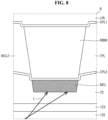
- a bank layer MBM is disposed on the first capping layer CPL1.
- the bank layer MBM may include an organic material.
- the bank layer MBM may include a light absorbing material that absorbs light in a visible wavelength band.
- the bank layer MBM may include an organic light blocking material.
- the bank layer MBM may be a type of light blocking member.
- the bank layer MBM is disposed along the boundaries of the sub-pixels PXS within a pixel PX, and each of the sub-pixels PXS may be distinguished from each other by portions of the bank layer MBM.
- the bank layer MBM may define the light blocking region BA and the light transmission region TA.
- the planar area where the bank layer MBM is disposed corresponds to the light blocking region BA.
- the color control layer WCL and TPL that is not covered by the bank layer MBM or is exposed by the bank layer MBM to outside thereof, may correspond to the light transmission region TA.
- the bank layer MBM includes or is made of a material capable of blocking light transmission, and serves to reduce or effectively prevent light from invading into sub-pixels PXS which are adjacent to each other and causing the color mixing.
- the bank layer MBM may serve as a partition wall that guides an ink material to be injected stably to a position in a direction along the second substrate 210.
- the bank layer MBM may include a plurality of holes penetrating the bank layer MBM along the thickness direction.
- the plurality of holes may be spaced apart from each other in a direction along the second substrate 210.
- the color control layer WCL and TPL or a spacer may be disposed in the plurality of holes.
- a hole in which the color control layer WCL and TPL is disposed is referred to as an opening, and a hole in which the spacer is disposed is referred to as a through hole.
- the bank layer MBM may define the opening in plural including openings OP1, OP2 and OP3 (e.g., first opening, second opening and third opening) that partially exposes the first capping layer CPL1 to outside the bank layer MBM.
- the openings OP1, OP2 and OP3 is disposed in the light transmission region TA and may be aligned with the light transmission region TA along the thickness direction.
- the openings OP1, OP2 and OP3 may overlap the color filter layers CFL along the thickness direction.
- the color filter layers CFL respectively overlapping the openings OP1, OP2 and OP3 may be any one of the first color filter layer CFL_1, the second color filter layer CFL_2 and the third color filter layer CFL_3.
- the openings OP1, OP2 and OP3 defined by the bank layer MBM may be provided in plural number, and each of the plurality of openings OP1, OP2 and OP3 may overlap or be aligned with any one of the first color filter layer CFL_1, the second color filter layer CFL_2 and the third color filter layer CFL_3.
- the bank layer MBM may protrude further than the color control layer WCL and TPL along the thickness direction, to define a protruded portion but is not limited thereto.
- the height (or thickness) of the protruded portion of the bank layer MBM relative to a pattern of the wavelength conversion layer WCL or the light transmitting layer TPL may be about 1 micrometer ( ⁇ m) to about 3 ⁇ m, about 1.4 ⁇ m to about 1.8 ⁇ m, or about 1.6 ⁇ m.
- the embodiment is not limited thereto.
- the color control layer WCL and TPL are respectively disposed in the openings OP1, OP2 and OP3 defined by the bank layer MBM.
- the color control layer WCL and TPL may include the wavelength conversion layer WCL that converts the wavelength of the incident light and/or a light transmitting layer TPL that maintains the wavelength of the incident light passing therethrough.
- the patterns of the wavelength conversion layer WCL or the light transmitting layer TPL may be disposed to be separated from each other for each of the sub-pixels PXS.
- the wavelength conversion layer WCL or the light transmitting layer TPL may overlap the emission region EMA and the light transmission region TA along the thickness direction.
- the wavelength conversion layer WCL or the light transmitting layer TPL which are adjacent to each other may be spaced apart from each other. The separation space may generally overlap the light blocking region BA.
- the wavelength conversion layer WCL may be disposed in the sub-pixels PXS in which the wavelength of light incident from the light emitting layer EML is converted due to the difference from the color of the sub-pixel PXS corresponding thereto.
- the light transmitting layer TPL may be disposed in the sub-pixel PXS in which the wavelength of light incident from the light emitting layer EML is the same as the color of the sub-pixel PXS corresponding thereto.
- FIG. 5 illustrates the light emitting layer EML of each of the sub-pixels PXS emits a third color, and shows the wavelength conversion layer WCL is disposed in the first sub-pixel PXS_1 and the second sub-pixel PXS_2 while the light transmitting layer TPL is disposed in the third sub-pixel PXS_3.
- the light emitting layer EML of each of the sub-pixels PXS emits light, such as ultraviolet light, having a wavelength different from the color of each of the sub-pixels PXS
- only the wavelength conversion layer WCL may be provided while the light transmitting layer TPL is omitted.
- the light emitting layer EML of each of the sub-pixels PXS when the light emitting layer EML of each of the sub-pixels PXS emits light corresponding to the color of each of the sub-pixels PXS, only the light transmitting layer TPL may be provided while the wavelength conversion layer WCL is omitted, or the light transmitting layer TPL may be omitted in all of the sub-pixels PXS.
- the wavelength conversion layer WCL may include a first wavelength conversion pattern WCL1 disposed in the first sub-pixel PXS_1 and a second wavelength conversion pattern WCL2 disposed in the second sub-pixel PXS_2 (e.g., wavelength conversion patterns WCL1 and WCL2).
- the color mixing prevention layer MCL may block at least a portion of light in a visible wavelength band.
- the color mixing prevention layer MCL (e.g., color absorbing pattern or color absorbing layer) may include a light absorbing material capable of absorbing at least a portion of light in a visible wavelength band.
- the light absorbing material may include, for example, a black dye, black pigment or the like, but is not limited thereto.
- the color mixing prevention layer MCL may absorb all light in a visible wavelength band. Therefore, the color mixing prevention layer MCL may block most of light in a visible wavelength band, for example, may block red light, green light, blue light and the like.
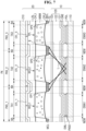
- the color mixing prevention layer MCL may block the light L directed to the bank layer MBM as a portion of the light L emitted from the light emitting layer EML disposed in the second emission region EMA2. Accordingly, suppression or effective prevention of a portion of the light L emitted from the light emitting layer EML disposed in the second emission region EMA2 from penetrating the bank layer MBM to enter the neighboring first wavelength conversion pattern WCL1 or light transmitting layer TPL is possible, thereby further suppressing or effectively preventing the color mixing between pixels PX and/or between sub-pixels PXS which are adjacent to each other, and improving the color matching rate of the display device 1.
- the color filter layers CFL may include the first color filter layer CFL_1, the second color filter layer CFL_2 and the third color filter layer CFL_3.
- the color filter layers CFL e.g., the first to third color filter layers CFL_1, CFL_2 and CFL_3 may be provided or formed by applying a photosensitive organic material including a colorant having a color and then exposing and developing the photosensitive organic material.
- the first to third color filter layers CFL_1, CFL_2 and CFL_3 may be provided or formed from the second substrate 210 in the order of the third color filter layer CFL_3, the first color filter layer CFL_1 and the second color filter layer CFL_2, although not limited thereto.
- the organic material layer from which the color mixing prevention layer MCL is provided layer may further include a light absorbing material. That is, the color mixing prevention layer MCL may be a patterned light absorbing layer.
- the color mixing prevention layer MCL may be provided or formed after the color control layer WCL and TPL and the second capping layer CPL2 are provided or formed. Accordingly, the color mixing prevention layer MCL does not directly contact the bank layer MBM having a lyophobic component, and the material layer from which the color mixing prevention layer MCL is provided may be patterned at a desired position on the second capping layer CPL2, thereby improving the reliability of the display device 1 (see FIG. 1 ).
- the filling layer 70 may be applied on the second capping layer CPL2 and the color mixing prevention layer MCL to bond the first display substrate 10 to the second display substrate 20. That is, a filler (e.g., the filling layer 70) covers a color absorbing layer (e.g., color mixing prevention layer MCL) and a layer which includes both the bank layer MBM and the wavelength control pattern and is in direct contact with the color absorbing layer. For convenience of explanation, repeated detailed description thereof will be omitted.
- a filler e.g., the filling layer 70
- a color absorbing layer e.g., color mixing prevention layer MCL
- FIG. 13 is a cross-sectional view of an embodiment of a display device 1_1. A description of the same components described above will be omitted or simplified, and differences will be mainly described.
- a display device 1_1 is different from that of the embodiment of FIG. 5 in that the display device 1_1 includes a color mixing prevention layer MCL_1, and the color mixing prevention layer MCL_1 transmits red light. That is, the color absorbing layer (e.g., color mixing prevention layer MCL_1) blocks both the blue light and the green light which is emitted from the light emitting element, and transmits red light.
- the color absorbing layer e.g., color mixing prevention layer MCL_1
- the color mixing prevention layer MCL_1 may include a light absorbing material, and the light absorbing material may include a red dye or a red pigment.
- the color mixing prevention layer MCL_1 may absorb and block blue light and green light, but may transmit red light.
- Light emitted from the light emitting layer EML includes one of blue light having a blue wavelength band or green light having a green wavelength band. Even if the color mixing prevention layer MCL_1 transmits red light, blue light and green light may be blocked. Therefore, the color mixing prevention layer MCL_1 may block the light from one of the pixels PX of sub-pixels PXS which is directed to another one of the pixels PX and/or an adjacent one of the sub pixels PXS, as a portion of the light emitted from the light emitting layer EML.
- the color mixing prevention layer MCL_1 Due to the color mixing prevention layer MCL_1, the color mixing between pixels PX and/or between sub-pixels PXS which are respectively adjacent to each other is further suppressed or effectively prevented, and the color matching rate of the display device 1_1 can be further improved.
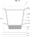
- FIG. 14 is an enlarged cross-sectional view showing an embodiment of an area of a display device 1_2.
- a display device 1_2 is different from that of the embodiment of FIG. 5 in that the display device 1_2 further includes a reflective layer RF_2 in addition to the color mixing prevention layer MCL.
- the display device 1_2 include the color mixing prevention layer MCL disposed below the bank layer MBM to be closer to the light emitting layer EML than the bank layer MBM, and may further include the reflective layer RF_2 disposed on the side surface or sidewall of the bank layer MBM which defines an opening thereof.
- the reflective layer RF_2 may be disposed on the side surface of the bank layer MBM and between the bank layer MBM and the color control layer WCL and TPL.
- the second capping layer CPL2 may cover the bank layer MBM and the color control layer WCL and TPL as well as the reflective layer RF_2.
- the second capping layer CPL2 may contact each of the bank layer MBM, the color control layer WCL and TPL and the reflective layer RF_2.
- the color mixing prevention layer MCL Due to the color mixing prevention layer MCL, the color mixing between pixels PX and/or between sub-pixels PXS which are respectively adjacent to each other is further suppressed or effectively prevented, and the color matching rate of the display device 1_2 can be further improved.
- the reflective layer RF_2 is further provided, light emitted from the light emitting layer EML (see FIG. 5 ) is reflected by the reflective layer RF_2 and directed to outside of the display device 1_2 without being absorbed into the bank layer MBM, thereby improving the light efficiency.
- FIG. 15 is a schematic plan view showing an embodiment of a pixel arrangement of a display device 1_3.
- a display device 1_3 is different from that of the embodiment of FIG. 4 in that the display device 1_3 includes a color mixing prevention layer MCL_3, and the color mixing prevention layer MCL_3 has substantially the same planar pattern as the light blocking region BA.
- the color mixing prevention layer MCL_3 may be disposed over the entire light blocking region BA.
- the color mixing prevention region MCA in which the color mixing prevention layer MCL_3 is disposed may be substantially the same as the light blocking region BA, in a plan view.
- the planar pattern of the color mixing prevention layer MCL_3 may be substantially the same as the planar pattern of the light blocking region BA.
- the color mixing prevention layer MCL_3 may be provided or formed in substantially the same pattern as the bank layer MBM (see FIG. 5 ), in a plan view.
- the color mixing prevention layer MCL_3 entirely overlaps the bank layer MBM (see FIG. 5 ), and may have the same planar area as the bank layer MBM in a plan view.
- the color mixing prevention layer MCL_3 Due to the color mixing prevention layer MCL_3, the color mixing between pixels PX and/or between sub-pixels PXS which are respectively adjacent to each other is further suppressed or effectively prevented, and the color matching rate of the display device 1_3 can be further improved.
Landscapes
- Physics & Mathematics (AREA)
- Engineering & Computer Science (AREA)
- Microelectronics & Electronic Packaging (AREA)
- General Physics & Mathematics (AREA)
- Optics & Photonics (AREA)
- Manufacturing & Machinery (AREA)
- Geometry (AREA)
- Electroluminescent Light Sources (AREA)
Claims (17)
- Anzeigevorrichtung (1), umfassend:ein erstes Anzeigesubstrat (10), beinhaltend ein lichtemittierendes Element (EML), das Licht einer ersten Farbe oder Licht einer zweiten Farbe, die sich von der ersten Farbe unterscheidet, emittiert; undein zweites Anzeigesubstrat (20), das dem ersten Anzeigesubstrat (10) zugewandt ist, wobei das zweite Anzeigesubstrat (20) in der Reihenfolge zu dem ersten Anzeigesubstrat (10) hingerichtet Folgendes beinhaltet:gekennzeichnet durcheine erste Deckschicht (CPL1);eine Schicht, beinhaltend die beiden Folgenden:eine Dammschicht (MBM) auf der ersten Deckschicht (CPL1), die eine Öffnung (OP) definiert; undein Wellenlängensteuermuster (WCL, TPL) in der Öffnung (OP);eine zweite Deckschicht (CPL2), die das Wellenlängensteuermuster (WCL, TPL) und die Dammschicht (MBM) bedeckt; undeine farbabsorbierende Schicht (MCL), welche die Dammschicht (MBM) überlappt und das Licht der ersten Farbe und das Licht der zweiten Farbe, das von dem lichtemittierenden Element (EML) emittiert wird, blockiert,
wobeidie zweite Deckschicht (CPL2) eine erste Fläche beinhaltet, welche die farbabsorbierende Schicht (MCL) überlappt,die Dammschicht (MBM) eine zweite Fläche beinhaltet, welche die farbabsorbierende Schicht (MCL) überlappt,die erste Deckschicht (CPL1) eine dritte Fläche beinhaltet, welche die farbabsorbierende Schicht (MCL) überlappt,sich die erste Fläche der zweiten Deckschicht (CPL2) zwischen der farbabsorbierenden Schicht (MCL) und der zweiten Fläche der Dammschicht (MBM) befindet unddie erste Fläche der zweiten Deckschicht (CPL2) und die dritte Fläche der ersten Deckschicht (CPL1) voneinander beabstandet sind, wobei die farbabsorbierende Schicht (MCL) dazwischen eingefügt ist. - Anzeigevorrichtung (1) nach Anspruch 1, wobeidie farbabsorbierende Schicht ein rotes Pigment oder einen roten Farbstoff beinhaltet und Licht einer dritten Farbe, die sich von der ersten Farbe und der zweiten Farbe unterscheidet, durchlässt unddie erste Farbe blau ist, die zweite Farbe grün ist und die dritte Farbe rot ist.
- Anzeigevorrichtung (1) nach mindestens einem der Ansprüche 1 oder 2, wobeidie farbabsorbierende Schicht (MCL) ein schwarzes Pigment oder einen schwarzen Farbstoff beinhaltet und Licht einer dritten Farbe, die sich von der ersten Farbe und der zweiten Farbe unterscheidet, blockiert, unddie erste Farbe blau ist, die zweite Farbe grün ist und die dritte Farbe rot ist.
- Anzeigevorrichtung (1) nach mindestens einem der Ansprüche 1 bis 3, wobei eine Gesamtheit der farbabsorbierenden Schicht (MCL) die Dammschicht (MBM) überlappt,die farbabsorbierende Schicht und die Dammschicht (MBM) jeweils eine ebene Fläche aufweisen, unddie ebene Fläche der farbabsorbierenden Schicht kleiner ist als die ebene Fläche der Dammschicht (MBM).
- Anzeigevorrichtung (1) nach Anspruch 4, wobeidie ebene Fläche der farbabsorbierenden Schicht (MCL) und die ebene Fläche der Dammschicht (MBM) jeweils ein ebenes Muster aufweisen, unddas ebene Muster der farbabsorbierenden Schicht sich von dem ebenen Muster der Dammschicht (MBM) unterscheidet.
- Anzeigevorrichtung (1) nach mindestens einem der Ansprüche 1 bis 5, ferner umfassend einen Füllstoff, der sich zwischen dem ersten Anzeigesubstrat (10) und dem zweiten Anzeigesubstrat (20) befindet,
wobei der Füllstoff die farbabsorbierende Schicht (MCL) und die Schicht bedeckt, die sowohl die Dammschicht (MBM) als auch das Wellenlängensteuermuster (WCL, TPL) beinhaltet und in direktem Kontakt mit der farbabsorbierenden Schicht (MCL) steht. - Anzeigevorrichtung (1) nach mindestens einem der Ansprüche 1 bis 6, wobei das lichtemittierende Element (EML) Folgendes beinhaltet:eine erste Elektrode (PXSE);eine zweite Elektrode (CME), die der ersten Elektrode (PXSE) zugewandt ist; undeine lichtemittierende Schicht (EML) zwischen der ersten Elektrode (PXSE) und der zweiten Elektrode (CME); undwobei das erste Anzeigesubstrat (10) ferner eine pixeldefinierende Schicht (PDL) beinhaltet, die eine Öffnung definiert, welche die erste Elektrode (PXSE) des lichtemittierenden Elements (EML) einem Bereich außerhalb der pixeldefinierenden Schicht (PDL) aussetzt.
- Anzeigevorrichtung (1) nach Anspruch 7, wobeidie lichtemittierende Schicht (EML) eine erste lichtemittierende Unterschicht (EML1) und eine zweite lichtemittierende Unterschicht (EML2) beinhaltet, die einander überlappen,die erste lichtemittierende Unterschicht (EML1) das Licht der ersten Farbe emittiert,die zweite lichtemittierende Unterschicht (EML2) das Licht der zweiten Farbe emittiert, unddie erste Farbe blau ist und die zweite Farbe grün ist.
- Anzeigevorrichtung (1) nach Anspruch 8, wobeidie lichtemittierende Schicht (EML) ferner eine dritte lichtemittierende Unterschicht (EML3) und eine vierte lichtemittierende Unterschicht (EML4) beinhaltet, die jeweils sowohl die erste lichtemittierende Unterschicht (EML1) als auch die zweite lichtemittierende Unterschicht (EML2) überlappen, undsowohl die dritte lichtemittierende Unterschicht (EML3) als auch die vierte lichtemittierende Unterschicht (EML4) das Licht der ersten Farbe emittieren.
- Anzeigevorrichtung (1) nach mindestens einem der Ansprüche 1 bis 9, ferner umfassend ein Pixel (PX), das Folgendes beinhaltet:ein erstes Unterpixel (PXS_1), von dem die erste Farbe emittiert wird,ein zweites Unterpixel (PXS_2), von dem die zweite Farbe emittiert wird,ein drittes Unterpixel (PXS_3), von dem eine dritte Farbe, die sich von der ersten Farbe und der zweiten Farbe unterscheidet, emittiert wird,einen ersten Lichtdurchlassbereich (TA1), der dem ersten Unterpixel (PXS_1) entspricht;einen zweiten Lichtdurchlassbereich (TA2), der dem zweiten Unterpixel (PXS_2) entspricht;einen dritten Lichtdurchlassbereich (TA3), der dem dritten Unterpixel (PXS_3) entspricht; undeinen Lichtblockierbereich (BA) rund um jeden des ersten Lichtdurchlassbereichs (TA1), des zweiten Lichtdurchlassbereichs (TA2) und des dritten Lichtdurchlassbereichs (TA3),wobei sich die farbabsorbierende Schicht in dem Lichtdurchlassbereich (BA) befindet.
- Anzeigevorrichtung (1) nach Anspruch 10, wobei innerhalb des Pixels (PX):der erste Lichtdurchlassbereich (TA1), der zweite Lichtdurchlassbereich (TA2) und der dritte Lichtdurchlassbereich (TA3) jeweils durch einen ersten Abstand voneinander getrennt sind, undder erste Abstand etwa 20 Mikrometer beträgt.
- Anzeigevorrichtung (1) nach Anspruch 11, ferner umfassend innerhalb des Pixels (PX):einen ersten Emissionsbereich innerhalb des ersten Lichtdurchlassbereichs,einen zweiten Emissionsbereich innerhalb des zweiten Lichtdurchlassbereichs und einen dritten Emissionsbereich innerhalb des dritten Lichtdurchlassbereichs, jeder des ersten Lichtdurchlassbereichs (TA1), des ersten Emissionsbereichs,des zweiten Lichtdurchlassbereichs (TA2), des zweiten Emissionsbereichs, des dritten Lichtdurchlassbereichs (TA3) und des dritten Emissionsbereichs eine Außenkante aufweist,die Außenkante des ersten Lichtdurchlassbereichs (TA1), des zweiten Lichtdurchlassbereichs (TA2) und des dritten Lichtdurchlassbereichs (TA3) jeweils von der Außenkante des ersten Emissionsbereichs, des zweiten Emissionsbereichs und des dritten Emissionsbereichs um einen zweiten Abstand beabstandet ist, undder zweite Abstand etwa 8 Mikrometer beträgt.
- Anzeigevorrichtung (1) nach mindestens einem der Ansprüche 10 bis 12, wobei innerhalb des Pixels (PX) die farbabsorbierende Schicht (MCL) den ersten Lichtdurchlassbereich (TA1) teilweise umgibt und sowohl den zweiten Lichtdurchlassbereich (TA2) als auch den dritten Lichtdurchlassbereich (TA3) vollständig umgibt.
- Anzeigevorrichtung (1) nach Anspruch 13, wobeidas Pixel (PX) in einer Vielzahl bereitgestellt ist, die ein erstes Pixel (PX1) und ein zweites Pixel (PX2) beinhaltet, die entlang einer ersten Richtung (DR1) benachbart zueinander sind, undsich die farbabsorbierende Schicht (MCL) in dem ersten Pixel (PX1) befindet und sich entlang der ersten Richtung (DR1) von dem ersten Pixel (PX1) erstreckt, um sich in dem zweiten Pixel (PX2) zu befinden.
- Verfahren zum Bereitstellen einer Anzeigevorrichtung (1), umfassend:Bereitstellen einer ersten Deckschicht (CPL1) auf einer Schicht mit geringer Brechung (LRL);Bereitstellen einer Dammschicht (MBM), die eine Öffnung auf der ersten Deckschicht (CPL1) definiert;Bereitstellen einer Farbsteuerschicht (WCL) in der Öffnung;Bereitstellen einer zweiten Deckschicht (CPL2), welche die Dammschicht (MBM) und die Farbsteuerschicht (WCL) bedeckt;gekennzeichnet durch die folgenden Schritte:nach dem Bereitstellen der zweiten Deckschicht (CPL2), Bereitstellen einer Schicht aus farbabsorbierendem Material (MCL) auf der zweiten Deckschicht (CPL2); undMustern der Schicht aus farbabsorbierendem Material (MCL) auf der zweiten Deckschicht (CPL2), um ein farbabsorbierendes Muster bereitzustellen, das die Dammschicht (MBM) überlappt,
wobeidie zweite Deckschicht (CPL2) eine erste Fläche beinhaltet, die das Farbabsorptionsmuster überlappt,die Dammschicht (MBM) eine zweite Fläche beinhaltet, die das Farbabsorptionsmuster überlappt, wobei die erste Deckschicht (CPL1) eine dritte Fläche beinhaltet, welche die farbabsorbierende Schicht (MCL) überlappt,die erste Fläche der zweiten Deckschicht (CPL2) sich zwischen dem farbabsorbierenden Muster und der zweiten Fläche der Dammschicht (MBM) befindet, unddie erste Fläche der zweiten Deckschicht (CPL2) und die dritte Fläche der ersten Deckschicht (CPL1) voneinander beabstandet sind, wobei die farbabsorbierende Schicht dazwischen eingefügt ist. - Verfahren nach Anspruch 15, wobei das Bereitstellen des farbabsorbierenden Musters Belichten und Entwickeln der Schicht aus farbabsorbierendem Material unter Verwendung einer Fotomaske umfasst.
- Verfahren nach Anspruch 16, wobei die Schicht aus farbabsorbierendem Material (MCL) ein rotes Pigment oder einen roten Farbstoff beinhaltet, blaues Licht und grünes Licht blockiert und rotes Licht durchlässt.
Applications Claiming Priority (1)
| Application Number | Priority Date | Filing Date | Title |
|---|---|---|---|
| KR1020200075574A KR102900590B1 (ko) | 2020-06-22 | 2020-06-22 | 표시 장치 및 표시 장치의 제조 방법 |
Publications (3)
| Publication Number | Publication Date |
|---|---|
| EP3929997A2 EP3929997A2 (de) | 2021-12-29 |
| EP3929997A3 EP3929997A3 (de) | 2022-05-04 |
| EP3929997B1 true EP3929997B1 (de) | 2025-04-02 |
Family
ID=76553513
Family Applications (1)
| Application Number | Title | Priority Date | Filing Date |
|---|---|---|---|
| EP21180605.4A Active EP3929997B1 (de) | 2020-06-22 | 2021-06-21 | Anzeigevorrichtung und verfahren zur bereitstellung davon |
Country Status (4)
| Country | Link |
|---|---|
| US (2) | US11903261B2 (de) |
| EP (1) | EP3929997B1 (de) |
| KR (1) | KR102900590B1 (de) |
| CN (1) | CN113903776A (de) |
Families Citing this family (20)
| Publication number | Priority date | Publication date | Assignee | Title |
|---|---|---|---|---|
| US11864443B2 (en) | 2019-10-04 | 2024-01-02 | Jdi Design And Development G. K. | Self-luminous display panel having different optical distances between light-shielding film and light emission reference points depending on light emission color |
| CN114582246B (zh) * | 2020-11-17 | 2025-03-18 | 京东方科技集团股份有限公司 | 显示面板及其制造方法和显示装置 |
| CN114582924B (zh) * | 2020-11-30 | 2025-07-29 | 华为技术有限公司 | 一种有机发光显示面板及显示装置 |
| KR102873653B1 (ko) * | 2020-12-11 | 2025-10-17 | 엘지디스플레이 주식회사 | 유기발광 표시장치 |
| KR20220169014A (ko) * | 2021-06-17 | 2022-12-27 | 삼성디스플레이 주식회사 | 색변환 기판 및 이를 포함하는 표시 장치 |
| KR20230103692A (ko) * | 2021-12-31 | 2023-07-07 | 엘지디스플레이 주식회사 | 발광 소자를 포함한 표시 장치 |
| KR20230127431A (ko) | 2022-02-24 | 2023-09-01 | 삼성디스플레이 주식회사 | 디스플레이 장치 |
| CN116998251A (zh) * | 2022-03-01 | 2023-11-03 | 京东方科技集团股份有限公司 | 彩膜基板、显示基板及其制造方法、显示装置 |
| KR20230146711A (ko) | 2022-04-12 | 2023-10-20 | 삼성디스플레이 주식회사 | 표시장치 |
| KR20230168225A (ko) | 2022-06-03 | 2023-12-13 | 삼성디스플레이 주식회사 | 색변환 기판, 이를 포함하는 표시 장치, 및 색변환 기판의 제조 방법 |
| KR20230172050A (ko) * | 2022-06-14 | 2023-12-22 | 삼성디스플레이 주식회사 | 표시장치 |
| KR20240042311A (ko) * | 2022-09-23 | 2024-04-02 | 삼성디스플레이 주식회사 | 색 제어 부재 및 이를 포함하는 표시 장치 |
| KR20240108078A (ko) * | 2022-12-30 | 2024-07-09 | 엘지디스플레이 주식회사 | 표시 장치 |
| CN116018000A (zh) * | 2023-02-06 | 2023-04-25 | 固安翌光科技有限公司 | 一种显示装置 |
| US12408488B2 (en) * | 2023-03-13 | 2025-09-02 | Mikro Mesa Technology Co., Ltd. | Micro light-emitting diode device |
| US12439740B2 (en) * | 2023-03-13 | 2025-10-07 | Mikro Mesa Technology Co., Ltd. | Micro light-emitting diode device |
| KR20240146138A (ko) * | 2023-03-27 | 2024-10-08 | 삼성디스플레이 주식회사 | 표시패널 |
| CN120323121A (zh) * | 2023-10-26 | 2025-07-15 | 京东方科技集团股份有限公司 | 色转换基板和显示装置 |
| KR20250108801A (ko) * | 2024-01-08 | 2025-07-16 | 삼성디스플레이 주식회사 | 표시 장치 및 이의 구동 방법 |
| KR20250123973A (ko) * | 2024-02-08 | 2025-08-19 | 삼성디스플레이 주식회사 | 표시 장치 |
Family Cites Families (14)
| Publication number | Priority date | Publication date | Assignee | Title |
|---|---|---|---|---|
| JP2009252406A (ja) * | 2008-04-02 | 2009-10-29 | Fuji Electric Holdings Co Ltd | 色変換フィルタ |
| JP2015128027A (ja) * | 2013-12-27 | 2015-07-09 | シャープ株式会社 | 有機el装置、表示装置 |
| EP3439042B1 (de) * | 2016-04-01 | 2021-07-28 | Seoul Semiconductor Co., Ltd. | Anzeigevorrichtung und herstellungsverfahren dafür |
| KR102783429B1 (ko) | 2017-01-25 | 2025-03-18 | 삼성디스플레이 주식회사 | 표시 장치 |
| KR102454192B1 (ko) | 2017-07-19 | 2022-10-13 | 삼성디스플레이 주식회사 | 색변환 패널 및 이를 포함하는 표시 장치 |
| KR102467651B1 (ko) | 2017-07-27 | 2022-11-16 | 삼성디스플레이 주식회사 | 표시 장치 및 그 제조 방법 |
| KR102617876B1 (ko) | 2018-02-01 | 2023-12-27 | 삼성디스플레이 주식회사 | 색변환 패널, 이를 포함하는 표시 장치 및 이의 제조 방법 |
| KR102708520B1 (ko) * | 2018-09-17 | 2024-09-23 | 삼성디스플레이 주식회사 | 표시 장치 |
| KR102747738B1 (ko) * | 2018-11-09 | 2025-01-02 | 삼성디스플레이 주식회사 | 표시 장치 및 이의 제조 방법 |
| KR102818046B1 (ko) * | 2018-11-19 | 2025-06-11 | 삼성디스플레이 주식회사 | 표시장치 |
| KR102758517B1 (ko) * | 2018-11-20 | 2025-01-24 | 삼성디스플레이 주식회사 | 표시 패널 |
| KR102807368B1 (ko) | 2019-04-02 | 2025-05-15 | 삼성디스플레이 주식회사 | 표시 장치 |
| KR102325381B1 (ko) | 2019-04-15 | 2021-11-10 | 삼성디스플레이 주식회사 | 표시 장치 |
| KR102815025B1 (ko) * | 2019-08-16 | 2025-05-30 | 삼성디스플레이 주식회사 | 표시 장치 |
-
2020
- 2020-06-22 KR KR1020200075574A patent/KR102900590B1/ko active Active
-
2021
- 2021-05-20 US US17/325,380 patent/US11903261B2/en active Active
- 2021-06-21 EP EP21180605.4A patent/EP3929997B1/de active Active
- 2021-06-22 CN CN202110691186.XA patent/CN113903776A/zh active Pending
-
2023
- 2023-11-28 US US18/520,805 patent/US12193279B2/en active Active
Also Published As
| Publication number | Publication date |
|---|---|
| CN113903776A (zh) | 2022-01-07 |
| EP3929997A2 (de) | 2021-12-29 |
| KR20210157932A (ko) | 2021-12-30 |
| US20210399068A1 (en) | 2021-12-23 |
| KR102900590B1 (ko) | 2025-12-16 |
| EP3929997A3 (de) | 2022-05-04 |
| US11903261B2 (en) | 2024-02-13 |
| US20240099074A1 (en) | 2024-03-21 |
| US12193279B2 (en) | 2025-01-07 |
Similar Documents
| Publication | Publication Date | Title |
|---|---|---|
| US12193279B2 (en) | Display device including color absorbing layer between capping and bank layers for improving color matching, and method of providing the same | |
| EP3913683B1 (de) | Anzeigevorrichtung und verfahren zur bereitstellung davon | |
| KR102406606B1 (ko) | 유기 발광 소자, 이를 포함하는 유기 발광 표시 장치, 및 이의 제조 방법 | |
| US20210050388A1 (en) | Display device | |
| EP4036983B1 (de) | Anzeigevorrichtung | |
| EP4016637B1 (de) | Anzeigevorrichtung | |
| KR20220096853A (ko) | 표시 장치 | |
| US12501810B2 (en) | Display panel and display apparatus | |
| CN113889515B (zh) | 显示装置 | |
| KR102752574B1 (ko) | 표시장치 | |
| US20250089513A1 (en) | Display Substrate, Manufacturing Method Therefor, and Display Device | |
| KR102935572B1 (ko) | 표시 장치 | |
| US11495775B2 (en) | Light-emitting device including encapsulation layers having different refractive indexes, method of manufacturing the same and electronic apparatus | |
| CN116806446A (zh) | 显示装置和显示装置制造方法 | |
| US20260136795A1 (en) | Display panel and displaying device | |
| EP4503895A1 (de) | Anzeigevorrichtung und verfahren zur herstellung davon | |
| JP2008098046A (ja) | 発光装置及び電子機器 | |
| KR20260057739A (ko) | 표시 장치 | |
| CN120130156A (zh) | 显示面板、显示装置 | |
| KR20260004656A (ko) | 표시 장치 | |
| KR20260004640A (ko) | 표시패널 및 이의 제조방법 | |
| KR20260028971A (ko) | 표시 장치 | |
| KR20250138329A (ko) | 표시 장치 및 이의 제조 방법 | |
| KR20250123973A (ko) | 표시 장치 |
Legal Events
| Date | Code | Title | Description |
|---|---|---|---|
| PUAI | Public reference made under article 153(3) epc to a published international application that has entered the european phase |
Free format text: ORIGINAL CODE: 0009012 |
|
| STAA | Information on the status of an ep patent application or granted ep patent |
Free format text: STATUS: THE APPLICATION HAS BEEN PUBLISHED |
|
| AK | Designated contracting states |
Kind code of ref document: A2 Designated state(s): AL AT BE BG CH CY CZ DE DK EE ES FI FR GB GR HR HU IE IS IT LI LT LU LV MC MK MT NL NO PL PT RO RS SE SI SK SM TR |
|
| PUAL | Search report despatched |
Free format text: ORIGINAL CODE: 0009013 |
|
| AK | Designated contracting states |
Kind code of ref document: A3 Designated state(s): AL AT BE BG CH CY CZ DE DK EE ES FI FR GB GR HR HU IE IS IT LI LT LU LV MC MK MT NL NO PL PT RO RS SE SI SK SM TR |
|
| RIC1 | Information provided on ipc code assigned before grant |
Ipc: H01L 51/50 20060101ALI20220401BHEP Ipc: H01L 51/52 20060101ALI20220401BHEP Ipc: H01L 27/32 20060101AFI20220401BHEP |
|
| STAA | Information on the status of an ep patent application or granted ep patent |
Free format text: STATUS: REQUEST FOR EXAMINATION WAS MADE |
|
| 17P | Request for examination filed |
Effective date: 20221104 |
|
| RBV | Designated contracting states (corrected) |
Designated state(s): AL AT BE BG CH CY CZ DE DK EE ES FI FR GB GR HR HU IE IS IT LI LT LU LV MC MK MT NL NO PL PT RO RS SE SI SK SM TR |
|
| P01 | Opt-out of the competence of the unified patent court (upc) registered |
Effective date: 20230516 |
|
| REG | Reference to a national code |
Ref country code: DE Ref legal event code: R079 Free format text: PREVIOUS MAIN CLASS: H01L0027320000 Ipc: H01L0027150000 Ref document number: 602021028399 Country of ref document: DE |
|
| GRAP | Despatch of communication of intention to grant a patent |
Free format text: ORIGINAL CODE: EPIDOSNIGR1 |
|
| STAA | Information on the status of an ep patent application or granted ep patent |
Free format text: STATUS: GRANT OF PATENT IS INTENDED |
|
| RIC1 | Information provided on ipc code assigned before grant |
Ipc: H10K 59/38 20230101ALI20241129BHEP Ipc: H10K 59/32 20230101ALI20241129BHEP Ipc: H01L 27/15 20060101AFI20241129BHEP |
|
| INTG | Intention to grant announced |
Effective date: 20241220 |
|
| GRAS | Grant fee paid |
Free format text: ORIGINAL CODE: EPIDOSNIGR3 |
|
| GRAA | (expected) grant |
Free format text: ORIGINAL CODE: 0009210 |
|
| STAA | Information on the status of an ep patent application or granted ep patent |
Free format text: STATUS: THE PATENT HAS BEEN GRANTED |
|
| AK | Designated contracting states |
Kind code of ref document: B1 Designated state(s): AL AT BE BG CH CY CZ DE DK EE ES FI FR GB GR HR HU IE IS IT LI LT LU LV MC MK MT NL NO PL PT RO RS SE SI SK SM TR |
|
| REG | Reference to a national code |
Ref country code: GB Ref legal event code: FG4D |
|
| REG | Reference to a national code |
Ref country code: IE Ref legal event code: FG4D |
|
| REG | Reference to a national code |
Ref country code: DE Ref legal event code: R096 Ref document number: 602021028399 Country of ref document: DE |
|
| REG | Reference to a national code |
Ref country code: NL Ref legal event code: FP |
|
| PGFP | Annual fee paid to national office [announced via postgrant information from national office to epo] |
Ref country code: NL Payment date: 20250520 Year of fee payment: 5 |
|
| PGFP | Annual fee paid to national office [announced via postgrant information from national office to epo] |
Ref country code: DE Payment date: 20250520 Year of fee payment: 5 |
|
| PGFP | Annual fee paid to national office [announced via postgrant information from national office to epo] |
Ref country code: GB Payment date: 20250520 Year of fee payment: 5 |
|
| PGFP | Annual fee paid to national office [announced via postgrant information from national office to epo] |
Ref country code: FR Payment date: 20250521 Year of fee payment: 5 |
|
| PGFP | Annual fee paid to national office [announced via postgrant information from national office to epo] |
Ref country code: AT Payment date: 20250721 Year of fee payment: 5 |
|
| REG | Reference to a national code |
Ref country code: AT Ref legal event code: MK05 Ref document number: 1782192 Country of ref document: AT Kind code of ref document: T Effective date: 20250402 |
|
| PG25 | Lapsed in a contracting state [announced via postgrant information from national office to epo] |
Ref country code: FI Free format text: LAPSE BECAUSE OF FAILURE TO SUBMIT A TRANSLATION OF THE DESCRIPTION OR TO PAY THE FEE WITHIN THE PRESCRIBED TIME-LIMIT Effective date: 20250402 Ref country code: PT Free format text: LAPSE BECAUSE OF FAILURE TO SUBMIT A TRANSLATION OF THE DESCRIPTION OR TO PAY THE FEE WITHIN THE PRESCRIBED TIME-LIMIT Effective date: 20250804 Ref country code: ES Free format text: LAPSE BECAUSE OF FAILURE TO SUBMIT A TRANSLATION OF THE DESCRIPTION OR TO PAY THE FEE WITHIN THE PRESCRIBED TIME-LIMIT Effective date: 20250402 |
|
| REG | Reference to a national code |
Ref country code: LT Ref legal event code: MG9D |
|
| PG25 | Lapsed in a contracting state [announced via postgrant information from national office to epo] |
Ref country code: GR Free format text: LAPSE BECAUSE OF FAILURE TO SUBMIT A TRANSLATION OF THE DESCRIPTION OR TO PAY THE FEE WITHIN THE PRESCRIBED TIME-LIMIT Effective date: 20250703 Ref country code: NO Free format text: LAPSE BECAUSE OF FAILURE TO SUBMIT A TRANSLATION OF THE DESCRIPTION OR TO PAY THE FEE WITHIN THE PRESCRIBED TIME-LIMIT Effective date: 20250702 |
|
| PG25 | Lapsed in a contracting state [announced via postgrant information from national office to epo] |
Ref country code: PL Free format text: LAPSE BECAUSE OF FAILURE TO SUBMIT A TRANSLATION OF THE DESCRIPTION OR TO PAY THE FEE WITHIN THE PRESCRIBED TIME-LIMIT Effective date: 20250402 |
|
| PG25 | Lapsed in a contracting state [announced via postgrant information from national office to epo] |
Ref country code: BG Free format text: LAPSE BECAUSE OF FAILURE TO SUBMIT A TRANSLATION OF THE DESCRIPTION OR TO PAY THE FEE WITHIN THE PRESCRIBED TIME-LIMIT Effective date: 20250402 |
|
| PG25 | Lapsed in a contracting state [announced via postgrant information from national office to epo] |
Ref country code: HR Free format text: LAPSE BECAUSE OF FAILURE TO SUBMIT A TRANSLATION OF THE DESCRIPTION OR TO PAY THE FEE WITHIN THE PRESCRIBED TIME-LIMIT Effective date: 20250402 |
|
| PG25 | Lapsed in a contracting state [announced via postgrant information from national office to epo] |
Ref country code: AT Free format text: LAPSE BECAUSE OF FAILURE TO SUBMIT A TRANSLATION OF THE DESCRIPTION OR TO PAY THE FEE WITHIN THE PRESCRIBED TIME-LIMIT Effective date: 20250402 |
|
| PG25 | Lapsed in a contracting state [announced via postgrant information from national office to epo] |
Ref country code: RS Free format text: LAPSE BECAUSE OF FAILURE TO SUBMIT A TRANSLATION OF THE DESCRIPTION OR TO PAY THE FEE WITHIN THE PRESCRIBED TIME-LIMIT Effective date: 20250702 |
|
| PG25 | Lapsed in a contracting state [announced via postgrant information from national office to epo] |
Ref country code: IS Free format text: LAPSE BECAUSE OF FAILURE TO SUBMIT A TRANSLATION OF THE DESCRIPTION OR TO PAY THE FEE WITHIN THE PRESCRIBED TIME-LIMIT Effective date: 20250802 |
|
| PG25 | Lapsed in a contracting state [announced via postgrant information from national office to epo] |
Ref country code: LV Free format text: LAPSE BECAUSE OF FAILURE TO SUBMIT A TRANSLATION OF THE DESCRIPTION OR TO PAY THE FEE WITHIN THE PRESCRIBED TIME-LIMIT Effective date: 20250402 |
|
| REG | Reference to a national code |
Ref country code: DE Ref legal event code: R097 Ref document number: 602021028399 Country of ref document: DE |
|
| PG25 | Lapsed in a contracting state [announced via postgrant information from national office to epo] |
Ref country code: SM Free format text: LAPSE BECAUSE OF FAILURE TO SUBMIT A TRANSLATION OF THE DESCRIPTION OR TO PAY THE FEE WITHIN THE PRESCRIBED TIME-LIMIT Effective date: 20250402 Ref country code: DK Free format text: LAPSE BECAUSE OF FAILURE TO SUBMIT A TRANSLATION OF THE DESCRIPTION OR TO PAY THE FEE WITHIN THE PRESCRIBED TIME-LIMIT Effective date: 20250402 |
|
| PG25 | Lapsed in a contracting state [announced via postgrant information from national office to epo] |
Ref country code: CZ Free format text: LAPSE BECAUSE OF FAILURE TO SUBMIT A TRANSLATION OF THE DESCRIPTION OR TO PAY THE FEE WITHIN THE PRESCRIBED TIME-LIMIT Effective date: 20250402 |
|
| PG25 | Lapsed in a contracting state [announced via postgrant information from national office to epo] |
Ref country code: EE Free format text: LAPSE BECAUSE OF FAILURE TO SUBMIT A TRANSLATION OF THE DESCRIPTION OR TO PAY THE FEE WITHIN THE PRESCRIBED TIME-LIMIT Effective date: 20250402 |
|
| PG25 | Lapsed in a contracting state [announced via postgrant information from national office to epo] |
Ref country code: RO Free format text: LAPSE BECAUSE OF FAILURE TO SUBMIT A TRANSLATION OF THE DESCRIPTION OR TO PAY THE FEE WITHIN THE PRESCRIBED TIME-LIMIT Effective date: 20250402 Ref country code: SK Free format text: LAPSE BECAUSE OF FAILURE TO SUBMIT A TRANSLATION OF THE DESCRIPTION OR TO PAY THE FEE WITHIN THE PRESCRIBED TIME-LIMIT Effective date: 20250402 |
|
| REG | Reference to a national code |
Ref country code: CH Ref legal event code: H13 Free format text: ST27 STATUS EVENT CODE: U-0-0-H10-H13 (AS PROVIDED BY THE NATIONAL OFFICE) Effective date: 20260127 |
|
| PG25 | Lapsed in a contracting state [announced via postgrant information from national office to epo] |
Ref country code: IT Free format text: LAPSE BECAUSE OF FAILURE TO SUBMIT A TRANSLATION OF THE DESCRIPTION OR TO PAY THE FEE WITHIN THE PRESCRIBED TIME-LIMIT Effective date: 20250402 |
|
| PG25 | Lapsed in a contracting state [announced via postgrant information from national office to epo] |
Ref country code: MC Free format text: LAPSE BECAUSE OF FAILURE TO SUBMIT A TRANSLATION OF THE DESCRIPTION OR TO PAY THE FEE WITHIN THE PRESCRIBED TIME-LIMIT Effective date: 20250402 |
|
| PLBE | No opposition filed within time limit |
Free format text: ORIGINAL CODE: 0009261 |
|
| STAA | Information on the status of an ep patent application or granted ep patent |
Free format text: STATUS: NO OPPOSITION FILED WITHIN TIME LIMIT |
|
| REG | Reference to a national code |
Ref country code: CH Ref legal event code: L10 Free format text: ST27 STATUS EVENT CODE: U-0-0-L10-L00 (AS PROVIDED BY THE NATIONAL OFFICE) Effective date: 20260211 |
|
| PG25 | Lapsed in a contracting state [announced via postgrant information from national office to epo] |
Ref country code: LU Free format text: LAPSE BECAUSE OF NON-PAYMENT OF DUE FEES Effective date: 20250621 |
|
| REG | Reference to a national code |
Ref country code: BE Ref legal event code: MM Effective date: 20250630 |
|
| 26N | No opposition filed |
Effective date: 20260105 |
|
| PG25 | Lapsed in a contracting state [announced via postgrant information from national office to epo] |
Ref country code: IE Free format text: LAPSE BECAUSE OF NON-PAYMENT OF DUE FEES Effective date: 20250621 |
|
| PG25 | Lapsed in a contracting state [announced via postgrant information from national office to epo] |
Ref country code: BE Free format text: LAPSE BECAUSE OF NON-PAYMENT OF DUE FEES Effective date: 20250630 |
|
| PG25 | Lapsed in a contracting state [announced via postgrant information from national office to epo] |
Ref country code: CH Free format text: LAPSE BECAUSE OF NON-PAYMENT OF DUE FEES Effective date: 20250630 |