EP3929925A1 - Read/write conversion circuit and drive method and storage device thereof - Google Patents
Read/write conversion circuit and drive method and storage device thereof Download PDFInfo
- Publication number
- EP3929925A1 EP3929925A1 EP20894037.9A EP20894037A EP3929925A1 EP 3929925 A1 EP3929925 A1 EP 3929925A1 EP 20894037 A EP20894037 A EP 20894037A EP 3929925 A1 EP3929925 A1 EP 3929925A1
- Authority
- EP
- European Patent Office
- Prior art keywords
- signal
- terminal
- switch unit
- power supply
- read
- Prior art date
- Legal status (The legal status is an assumption and is not a legal conclusion. Google has not performed a legal analysis and makes no representation as to the accuracy of the status listed.)
- Granted
Links
Images




Classifications
-
- G—PHYSICS
- G11—INFORMATION STORAGE
- G11C—STATIC STORES
- G11C5/00—Details of stores covered by group G11C11/00
- G11C5/02—Disposition of storage elements, e.g. in the form of a matrix array
- G11C5/025—Geometric lay-out considerations of storage- and peripheral-blocks in a semiconductor storage device
-
- G—PHYSICS
- G06—COMPUTING OR CALCULATING; COUNTING
- G06F—ELECTRIC DIGITAL DATA PROCESSING
- G06F13/00—Interconnection of, or transfer of information or other signals between, memories, input/output devices or central processing units
- G06F13/38—Information transfer, e.g. on bus
- G06F13/40—Bus structure
- G06F13/4004—Coupling between buses
- G06F13/4022—Coupling between buses using switching circuits, e.g. switching matrix, connection or expansion network
-
- G—PHYSICS
- G11—INFORMATION STORAGE
- G11C—STATIC STORES
- G11C11/00—Digital stores characterised by the use of particular electric or magnetic storage elements; Storage elements therefor
- G11C11/21—Digital stores characterised by the use of particular electric or magnetic storage elements; Storage elements therefor using electric elements
- G11C11/34—Digital stores characterised by the use of particular electric or magnetic storage elements; Storage elements therefor using electric elements using semiconductor devices
- G11C11/40—Digital stores characterised by the use of particular electric or magnetic storage elements; Storage elements therefor using electric elements using semiconductor devices using transistors
- G11C11/401—Digital stores characterised by the use of particular electric or magnetic storage elements; Storage elements therefor using electric elements using semiconductor devices using transistors forming cells needing refreshing or charge regeneration, i.e. dynamic cells
- G11C11/4063—Auxiliary circuits, e.g. for addressing, decoding, driving, writing, sensing or timing
- G11C11/407—Auxiliary circuits, e.g. for addressing, decoding, driving, writing, sensing or timing for memory cells of the field-effect type
- G11C11/409—Read-write [R-W] circuits
-
- G—PHYSICS
- G11—INFORMATION STORAGE
- G11C—STATIC STORES
- G11C11/00—Digital stores characterised by the use of particular electric or magnetic storage elements; Storage elements therefor
- G11C11/21—Digital stores characterised by the use of particular electric or magnetic storage elements; Storage elements therefor using electric elements
- G11C11/34—Digital stores characterised by the use of particular electric or magnetic storage elements; Storage elements therefor using electric elements using semiconductor devices
- G11C11/40—Digital stores characterised by the use of particular electric or magnetic storage elements; Storage elements therefor using electric elements using semiconductor devices using transistors
- G11C11/401—Digital stores characterised by the use of particular electric or magnetic storage elements; Storage elements therefor using electric elements using semiconductor devices using transistors forming cells needing refreshing or charge regeneration, i.e. dynamic cells
- G11C11/4063—Auxiliary circuits, e.g. for addressing, decoding, driving, writing, sensing or timing
- G11C11/407—Auxiliary circuits, e.g. for addressing, decoding, driving, writing, sensing or timing for memory cells of the field-effect type
- G11C11/409—Read-write [R-W] circuits
- G11C11/4096—Input/output [I/O] data management or control circuits, e.g. reading or writing circuits, I/O drivers or bit-line switches
-
- G—PHYSICS
- G11—INFORMATION STORAGE
- G11C—STATIC STORES
- G11C7/00—Arrangements for writing information into, or reading information out from, a digital store
- G11C7/10—Input/output [I/O] data interface arrangements, e.g. I/O data control circuits, I/O data buffers
- G11C7/1048—Data bus control circuits, e.g. precharging, presetting, equalising
-
- G—PHYSICS
- G11—INFORMATION STORAGE
- G11C—STATIC STORES
- G11C7/00—Arrangements for writing information into, or reading information out from, a digital store
- G11C7/10—Input/output [I/O] data interface arrangements, e.g. I/O data control circuits, I/O data buffers
- G11C7/1051—Data output circuits, e.g. read-out amplifiers, data output buffers, data output registers, data output level conversion circuits
- G11C7/1069—I/O lines read out arrangements
-
- G—PHYSICS
- G11—INFORMATION STORAGE
- G11C—STATIC STORES
- G11C7/00—Arrangements for writing information into, or reading information out from, a digital store
- G11C7/10—Input/output [I/O] data interface arrangements, e.g. I/O data control circuits, I/O data buffers
- G11C7/1078—Data input circuits, e.g. write amplifiers, data input buffers, data input registers, data input level conversion circuits
- G11C7/1096—Write circuits, e.g. I/O line write drivers
-
- G—PHYSICS
- G11—INFORMATION STORAGE
- G11C—STATIC STORES
- G11C7/00—Arrangements for writing information into, or reading information out from, a digital store
- G11C7/10—Input/output [I/O] data interface arrangements, e.g. I/O data control circuits, I/O data buffers
- G11C7/1015—Read-write modes for single port memories, i.e. having either a random port or a serial port
- G11C7/1042—Read-write modes for single port memories, i.e. having either a random port or a serial port using interleaving techniques, i.e. read-write of one part of the memory while preparing another part
Definitions
- the present invention relates to the field of storage technologies, and in particular, to a read-write conversion circuit, a read-write conversion circuit driving method, and a memory.
- FIG. 1 is a schematic structural diagram of a dynamic random-access memory in the related art.
- the dynamic random-access memory usually includes a memory array 01, an SA (sense amplifier) array 02, an XDEC (row decoding circuit) 04, a YDEC (column decoding circuit) 03, and a read amplification circuit and write driver (SSA & write driver) circuit 05 of Gdata & Gdata# signals.
- FIG. 2 is a partially enlarged diagram of FIG. 1 . After a word line (WL) is selected (through XDEC decoding control), data is transmitted to the SAs on both upper and lower sides and is amplified by the SAs. Then, the amplified data is written back to a cell unit connected to the selected WL.
- WL word line
- a corresponding SA is selected through the YDEC column decoding, and the data is transmitted by a group of Gdata & Gdata# to a group of Ldata & Ldata# by using a local read-write conversion circuit (lrwap), and then written to a corresponding SA and a connected cell unit.
- the data transmission may follow an opposite direction.
- a corresponding SA is selected through YDEC column decoding, and the data is transmitted to a group of Ldata & Ldata#, and then is transmitted to a group of Gdata &Gdata# by using a local read-write conversion circuit (lrwap). Finally, the data is amplified and output by an SSA (second sense amplifier).
- FIG. 3 is a schematic structural diagram of an exemplary embodiment of a read-write conversion circuit in the related art.
- a signal may be read from a signal terminal Ldata to a signal terminal Gdata, and a signal may be read from a signal terminal Ldata# to a signal terminal Gdata#; and a signal on the signal terminal Gdata may be written to the signal terminal Ldata, and a signal on the signal terminal Gdata# may be written to the signal terminal Ldata#.
- the read-write conversion circuit may first write a reset voltage, through transistors T8, T9, and T10, to the signal terminals Ldata and Ldata#.
- a valid level may be input to a signal terminal Wr to turn on transistors T1 and T2, so that a signal from the signal terminal Gdata may be written to the signal terminal Ldata, and a signal from the signal terminal Gdata# may be written to the signal terminal Ldata#.
- the read-write conversion circuit may first write a high-level signal to the signal terminals Gdata and the Gdata#. Then, a valid level may be input to a signal terminal Rd to turn on transistors T4, T6, and T7.
- T3 When the signal terminal Ldata# is at a high level and Ldata is at a low level, T3 is turned on by the signal terminal Ldata#, so that a low-level signal from a ground terminal GND may be transmitted to the signal terminal Gdata. Simultaneously, T5 may be turned off by the signal terminal Ldata, and Gdata# may be kept at a high level. Likewise, when the signal terminal Ldata# is at a low level and Ldata is at a high level, Gdata# may be at a low level, and Gdata may be at a high level.
- the read-write conversion circuit in the read-write conversion circuit, during data writing and data reading, the signal terminals Gdata and Gdata# need to be in opposite complementary polarities. That is, levels of signals on the signal terminals Gdata and Gdata# need to be logically opposite.
- the read-write conversion circuit has a relatively slow read-write speed, and a precharge driver component and a write driver component that are connected to the read-write conversion circuit have relatively large sizes and relatively high power consumption.
- a read-write conversion circuit may include a first precharge circuit, a positive feedback circuit, a second precharge circuit, a fourth switch unit, a sixth switch unit, a seventh switch unit, an eighth switch unit, a tenth switch unit, an eleventh switch unit, a twelfth switch unit, a thirteenth switch unit, a fourteenth switch unit, and a fifteenth switch unit.
- the first precharge circuit may be connected to a first precharge control terminal, a first power supply terminal, a first signal terminal, and a second signal terminal, and is configured to transmit a signal of the first power supply terminal to the first signal terminal and the second signal terminal in response to a signal of the first precharge control terminal.
- the positive feedback circuit may be connected to the first signal terminal, the second signal terminal, and a second power supply terminal, and is configured to transmit a signal of the second power supply terminal to the second signal terminal in response to a signal of the first signal terminal and simultaneously disconnect the first signal terminal and the second power supply terminal in response to a signal of the second signal terminal, and configured to transmit a signal of the second power supply terminal to the first signal terminal in response to a signal of the second signal terminal and simultaneously disconnect the second signal terminal and the second power supply terminal in response to a signal of the first signal terminal.
- the second precharge circuit may be configured to precharge a voltage to a third signal terminal and a fourth signal terminal.
- the fourth switch unit may have a control terminal connected to a first write control terminal, a first terminal connected to the third signal terminal, and a second terminal connected to the first signal terminal.
- the sixth switch unit may have a control terminal connected to the third signal terminal, and a first terminal connected to the second signal terminal.
- the seventh switch unit may have a control terminal connected to the first write control terminal, a first terminal connected to a second terminal of the sixth switch unit, and a second terminal connected to a third power supply terminal.
- the eighth switch unit may have a control terminal connected to a second write control terminal, a first terminal connected to the second signal terminal, and a second terminal connected to the fourth signal terminal.
- the tenth switch unit may have a control terminal connected to the fourth signal terminal, and a first terminal connected to the first signal terminal.
- the eleventh switch unit may have a control terminal connected to the second write control terminal, a first terminal connected to a second terminal of the tenth switch unit, and a second terminal connected to the third power supply terminal.
- the twelfth switch unit may have a control terminal connected to the second signal terminal, and a first terminal connected to the third signal terminal.
- the thirteenth switch unit may have a control terminal connected to a first read control terminal, a first terminal connected to a second terminal of the twelfth switch unit, and a second terminal connected to the third power supply terminal.
- the fourteenth switch unit may have a control terminal connected to the first signal terminal, and a first terminal connected to the fourth signal terminal.
- the fifteenth switch unit may have a control terminal connected to a second read control terminal, a first terminal connected to a second terminal of the fourteenth switch unit, and a second terminal connected to the third power supply terminal.
- the first precharge circuit may include a first switch unit, a second switch unit, and a third switch unit.
- the first switch unit may have a control terminal connected to the first precharge control terminal, a first terminal connected to the first power supply terminal, and a second terminal connected to the first signal terminal.
- the second switch unit may have a control terminal connected to the first precharge control terminal, a first terminal connected to the first power supply terminal, and a second terminal connected to the second signal terminal.
- the third switch unit may have a control terminal connected to the first precharge control terminal, a first terminal connected to the first signal terminal, and a second terminal connected to the second signal terminal.
- the positive feedback circuit may include a fifth switch unit and a ninth switch unit.
- the fifth switch unit may have a control terminal connected to the first signal terminal, a first terminal connected to the second power supply terminal, and a second terminal connected to the second signal terminal.
- the ninth switch unit may have a control terminal connected to the second signal terminal, a first terminal connected to the second power supply terminal, and a second terminal connected to the first signal terminal.
- the fifth switch unit may be a P-type transistor
- the sixth switch unit is an N-type transistor.
- the signal of the second power supply terminal may be a high-level signal
- a signal of the third power supply terminal may be a low-level signal.
- the fifth switch unit may be an N-type transistor, and the sixth switch unit may be a P-type transistor.
- the signal of the second power supply terminal may be a low-level signal, and a signal of the third power supply terminal may be a high-level signal.
- the ninth switch unit may be a P-type transistor, and the tenth switch unit may be an N-type transistor.
- the signal of the second power supply terminal may be a high-level signal, and a signal of the third power supply terminal may be a low-level signal.
- the ninth switch unit may be an N-type transistor, and the tenth switch unit may be a P-type transistor.
- the signal of the second power supply terminal may be a low-level signal, and a signal of the third power supply terminal may be a high-level signal.
- the twelfth switch unit may be an N-type transistor.
- the signal of the third power supply terminal may be a low-level signal, and the second precharge circuit may be configured to precharge a high-level signal to the third signal terminal and the fourth signal terminal.
- the twelfth switch unit may be a P-type transistor.
- the signal of the third power supply terminal may be a high-level signal, and the second precharge circuit may be configured to precharge a low-level signal to the third signal terminal and the fourth signal terminal.
- the fourteenth switch unit may be an N-type transistor.
- the signal of the third power supply terminal may be a low-level signal, and the second precharge circuit may be configured to precharge a high-level signal to the third signal terminal and the fourth signal terminal.
- the fourteenth switch unit may be a P-type transistor.
- the signal of the third power supply terminal may be a high-level signal, and the second precharge circuit may be configured to precharge a low-level signal to the third signal terminal and the fourth signal terminal.
- a read-write conversion circuit driving method for driving any one of the foregoing read-write conversion circuits.
- the method may include a signal write stage and a signal read stage.
- the signal write stage may include a first write stage and a second write stage.
- the first write stage may include inputting a valid level signal to the first precharge control terminal to transmit a signal of the first power supply terminal to the first signal terminal and the second signal terminal in response to the valid level signal of the first precharge control terminal by using the first precharge circuit.
- the second write stage may include inputting a first to-be-written signal to the third signal terminal to transmit the first to-be-written signal of the third signal terminal to the first signal terminal in response to a signal of the first write control terminal and transmit a signal of the second power supply terminal to the second signal terminal in response to a signal of the first signal terminal, or transmit a signal of the third power supply terminal to the second signal terminal in response to a signal of the first write control terminal and a signal of the third signal terminal; and simultaneously writing a second to-be-written signal to the fourth signal terminal.
- the second write stage may include inputting a third to-be-written signal to the fourth signal terminal to transmit the third to-be-written signal of the fourth signal terminal to the second signal terminal in response to a signal of the second write control terminal and transmit a signal of the second power supply terminal to the first signal terminal in response to a signal of the second signal terminal, or transmit a signal of the third power supply terminal to the first signal terminal in response to a signal of the second write control terminal and a signal of the fourth signal terminal; and simultaneously writing a fourth to-be-written signal to the third signal terminal.
- the signal read stage may include a first read stage and a second read stage.
- the first read stage may include precharging a voltage to the third signal terminal and the fourth signal terminal by using the second precharge circuit.
- the second read stage may include inputting a valid level signal to the first read control terminal to transmit a signal of the third power supply terminal to the third signal terminal in response to a signal of the second signal terminal and a signal of the first read control terminal; and simultaneously precharging a voltage to the fourth signal terminal by using the second precharge circuit.
- the second read stage may include inputting a valid level signal to the second read control terminal to transmit a signal of the third power supply terminal to the fourth signal terminal in response to a signal of the first signal terminal and a signal of the second read control terminal; and simultaneously precharging a voltage to the third signal terminal by using the second precharge circuit.
- a memory is provided.
- the memory may include any one of the foregoing read-write conversion circuits.
- a read-write conversion circuit In the read-write conversion circuit, corresponding signals can be read from a third signal terminal and a fourth signal terminal by using only one of a first signal terminal or a second signal terminal in a signal read stage, and corresponding signals can be written to the first signal terminal and the second signal terminal by using only one of the third signal terminal or the fourth signal terminal in a signal write stage.
- FIG. 4 is a schematic structural diagram of an exemplary embodiment of a read-write conversion circuit according to the present invention.
- the read-write conversion circuit may include a first precharge circuit 1, a positive feedback circuit 2, a second precharge circuit 3, a fourth switch unit T4, a sixth switch unit T6, a seventh switch unit T7, an eighth switch unit T8, a tenth switch unit T10, an eleventh switch unit T11, a twelfth switch unit T12, a thirteenth switch unit T13, a fourteenth switch unit T14, and a fifteenth switch unit T15.
- the first precharge circuit 1 may be connected to a first precharge control terminal PreEqN, a first power supply terminal VI, a first signal terminal Ldata, and a second signal terminal Ldata#.
- the first precharge circuit 1 may be configured to transmit a signal of the first power supply terminal V1 to the first signal terminal Ldata and the second signal terminal Ldata# in response to a signal of the first precharge control terminal PreEqN.
- the positive feedback circuit 2 may be connected to the first signal terminal Ldata, the second signal terminal Ldata#, and a second power supply terminal V2.
- the positive feedback circuit 2 may be configured to transmit a signal of the second power supply terminal V2 to the second signal terminal Ldata# in response to a signal of the first signal terminal Ldata and simultaneously disconnect the first signal terminal Ldata and the second power supply terminal V2 in response to a signal of the second signal terminal Ldata#.
- the positive feedback circuit 2 may be further configured to transmit a signal of the second power supply terminal V2 to the first signal terminal Ldata in response to a signal of the second signal terminal Ldata# and simultaneously disconnect the second signal terminal Ldata# and the second power supply terminal V2 in response to a signal of the first signal terminal Ldata.
- the second precharge circuit 3 may be configured to precharge a voltage to a third signal terminal Gdata and a fourth signal terminal Gdata#.
- the fourth switch unit T4 may have a control terminal connected to a first write control terminal Wr1, a first terminal connected to the third signal terminal Gdata, and a second terminal connected to the first signal terminal Ldata.
- the sixth switch unit T6 may have a control terminal connected to the third signal terminal Gdata, and a first terminal connected to the second signal terminal Ldata#.
- the seventh switch unit T7 may have a control terminal connected to the first write control terminal Wr1, a first terminal connected to a second terminal of the sixth switch unit T6, and a second terminal connected to a third power supply terminal V3.
- the eighth switch unit T8 may have a control terminal connected to a second write control terminal Wr2, a first terminal connected to the second signal terminal Ldata#, and a second terminal connected to the fourth signal terminal Gdata#.
- the tenth switch unit T10 may have a control terminal connected to the fourth signal terminal Gdata#, and a first terminal connected to the first signal terminal Ldata.
- the eleventh switch unit T11 may have a control terminal connected to the second write control terminal Wr2, a first terminal connected to a second terminal of the tenth switch unit T10, and a second terminal connected to the third power supply terminal V3.
- the twelfth switch unit T12 may have a control terminal connected to the second signal terminal Ldata#, and a first terminal connected to the third signal terminal Gdata.
- the thirteenth switch unit T13 may have a control terminal connected to a first read control terminal Rd1, a first terminal connected to a second terminal of the twelfth switch unit T12, and a second terminal connected to the third power supply terminal V3.
- the fourteenth switch unit T14 may have a control terminal connected to the first signal terminal Ldata, and a first terminal connected to the fourth signal terminal Gdata#.
- the fifteenth switch unit T15 may have a control terminal connected to a second read control terminal Rd2, a first terminal connected to a second terminal of the fourteenth switch unit T14, and a second terminal connected to the third power supply terminal V3.
- the present invention provides a read-write conversion circuit.
- corresponding signals can be read from a third signal terminal and a fourth signal terminal by using only one of a first signal terminal or a second signal terminal in a signal read stage, and corresponding signals can be written to the first signal terminal and the second signal terminal by using only one of the third signal terminal or the fourth signal terminal in a signal write stage.
- a usage period of the third signal terminal and the fourth signal terminal increases from the original tCCD (an interval between adjacent write commands) to tCCD ⁇ 2.
- the time sequence requirement can be significantly relaxed, or, in other words, the read-write speed can be further improved.
- a precharge or prewrite operation may be performed on the third or the fourth signal terminals that is idle so that a read-write signal has more time to work, thereby reducing the sizes and the power consumption of the precharge driver component and the write driver component.
- the first precharge circuit 1 may include a first switch unit T1, a second switch unit T2, and a third switch unit T3.
- the first switch unit T1 may have a control terminal connected to the first precharge control terminal PreEqN, a first terminal connected to the first power supply terminal VI, and a second terminal connected to the first signal terminal Ldata.
- the second switch unit T2 may have a control terminal connected to the first precharge control terminal PreEqN, a first terminal connected to the first power supply terminal VI, and a second terminal connected to the second signal terminal Ldata#.
- the third switch unit T3 may have a control terminal connected to the first precharge control terminal PreEqN, a first terminal connected to the first signal terminal Ldata, and a second terminal connected to the second signal terminal Ldata#.
- a precharge operation may need to be performed on the read-write conversion circuit before read-write driving.
- a valid level signal may be input to the first precharge control terminal PreEqN to turn on the first switch unit T1, the second switch unit T2, and the third switch unit T3.
- the first power supply terminal V1 may precharge a reset level to the first signal terminal Ldata and the second signal terminal Ldata#.
- the positive feedback circuit 2 may include a fifth switch unit T5 and a ninth switch unit T9.
- the fifth switch unit T5 may have a control terminal connected to the first signal terminal Ldata, a first terminal connected to the second power supply terminal V2, and a second terminal connected to the second signal terminal Ldata#.
- the ninth switch unit T9 may have a control terminal connected to the second signal terminal Ldata#, a first terminal connected to the second power supply terminal V2, and a second terminal connected to the first signal terminal Ldata.
- the fifth switch unit T5 may be a P-type transistor, and the sixth switch unit may be an N-type transistor.
- the signal of the second power supply terminal V2 may be a high-level signal
- a signal of the third power supply terminal V3 may be a low-level signal.
- signals can be written to the first signal terminal Ldata and the second signal terminal Ldata# by using the third signal terminal Gdata.
- a valid level signal may be input to Wr1 to turn on the fourth switch unit T4 and the seventh switch unit T7 to transmit the signal of the third signal terminal Gdata to the first signal terminal Ldata.
- the high-level signal of the third signal terminal Gdata may cause the sixth switch unit to be turned on to transmit the low-level signal of the third power supply terminal V3 to the second signal terminal Ldata#.
- a valid level signal may be input to Wr1 to turn on the fourth switch unit T4 to transmit the signal of the third signal terminal Gdata to the first signal terminal Ldata.
- the low-level signal of the first signal terminal Ldata may cause the fifth switch unit T5 to be turned on to transmit the high-level signal of the second power supply terminal V2 to the second signal terminal Ldata#.
- the high-level signal of the second signal terminal Ldata# may cause the ninth switch unit T9 to be turned off so that the low-level signal of the first signal terminal Ldata may not be affected by the high-level signal of the second power supply terminal V2.
- the ninth switch unit may be a P-type transistor, and the tenth switch unit may be an N-type transistor.
- the signal of the second power supply terminal V2 may be a high-level signal
- a signal of the third power supply terminal V3 may be a low-level signal.
- signals can be written to the first signal terminal Ldata and the second signal terminal Ldata# by using the fourth signal terminal Gdata#.
- a valid level signal is input to Wr2 to close the eighth switch unit T8 and the eleventh switch unit T11 to transmit the signal of the fourth signal terminal Gdata# to the second signal terminal Ldata#.
- the high-level signal of the fourth signal terminal Gdata# may cause the tenth switch unit T10 to be closed to transmit the low-level signal of the third power supply terminal V3 to the first signal terminal Ldata.
- a valid level signal may be input to Wr2 to close the eighth switch unit T8 to transmit the signal of the fourth signal terminal Gdata# to the second signal terminal Ldata#.
- the low-level signal of the second signal terminal Ldata# may cause the ninth switch unit T9 to be closed to transmit the high-level signal of the second power supply terminal V2 to the first signal terminal Ldata.
- the high-level signal of the first signal terminal Ldata may cause the fifth switch unit T5 to be open so that the low-level signal of the second signal terminal Ldata# may not be affected by the high-level signal of the second power supply terminal V2.
- the twelfth switch unit may be an N-type transistor.
- a signal of the third power supply terminal V3 may be a low-level signal
- the second precharge circuit 3 may be configured to precharge a high-level signal to the third signal terminal Gdata and the fourth signal terminal Gdata#.
- signals can be read from the third signal terminal Gdata and the fourth signal terminal Gdata# by using the second signal terminal Ldata#.
- the twelfth switch unit T12 may be turned on.
- a valid level signal may be input to the first read control terminal Rd1 to turn on the thirteenth switch unit T13 to transmit the low-level signal of the third power supply terminal V3 to the third signal terminal Gdata.
- the fourth signal terminal Gdata# may maintain the high-level signal that is precharged by the second precharge circuit to the fourth signal terminal Gdata#.
- the fourteenth switch unit may be an N-type transistor.
- a signal of the third power supply terminal V3 may be a low-level signal
- the second precharge circuit 3 may be configured to precharge a high-level signal to the third signal terminal Gdata and the fourth signal terminal Gdata#.
- signals can be read from the third signal terminal Gdata and the fourth signal terminal Gdata# by using the first signal terminal Ldata.
- the fourteenth switch unit T14 may be turned on.
- a valid level signal may be input to the second read control terminal Rd2 to turn on the fifteenth switch unit T15 to transmit the low-level signal of the third power supply terminal V3 to the fourth signal terminal Gdata#.
- the third signal terminal Gdata may maintain the high-level signal that is precharged by the second precharge circuit to the third signal terminal Gdata.
- the first switch unit T1, the second switch unit T2, the third switch unit T3, the fourth switch unit T4, the seventh switch unit T7, the eighth switch unit T8, the ninth switch unit T9, the eleventh switch unit T11, the thirteenth switch unit T13, and the fifteenth switch unit T15 may be P-type transistors or N-type transistors.
- the first switch unit T1, the second switch unit T2, and the third switch unit T3 may be P-type transistors
- the fourth switch unit T4, the seventh switch unit T7, the eighth switch unit T8, the ninth switch unit T9, the eleventh switch unit T11, the thirteenth switch unit T13, and the fifteenth switch unit T15 may be N-type transistors.
- a driving method of the read-write conversion circuit may include a signal read stage and a signal write stage.
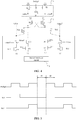
- FIG. 5 is a time sequence diagram of nodes in an exemplary embodiment of a read-write conversion circuit according to the present invention.
- the signal write stage may include a first write stage t1 and a second write stage t2.
- the first precharge control terminal PreEqN may be at a low level
- the first write control terminal Wr1 and the second write control terminal Wr2 may be at a low level
- the first precharge circuit may precharge a reset signal to the first signal terminal Ldata and the second signal terminal Ldata#.
- the first write control terminal Wr1 may be at a high level, and the second write control terminal Wr2 may be at a low level, so that signals can be written to the first signal terminal Ldata and the second signal terminal Ldata# by using the third signal terminal Gdata.
- the fourth signal terminal Gdata# may be a free terminal, and a data signal may be precharged to the fourth signal terminal Gdata# to write signals to the first signal terminal Ldata and the second signal terminal Ldata# by using the fourth signal terminal Gdata# in the next signal write stage.
- FIG. 6 is a time sequence diagram of nodes in another exemplary embodiment of a read-write conversion circuit according to the present invention.
- the signal read stage includes a first read stage t1 and a second read stage t2.
- the second precharge circuit may precharge a high-level signal to the third signal terminal Gdata and the fourth signal terminal Gdata#.
- a high-level signal may be input to the first read control terminal Rd1 to turn on the thirteenth switch unit, and the high-level signal of the second signal terminal Ldata# may cause the twelfth switch unit T12 to be turned on to transmit a low-level signal of the third power supply terminal to the third signal terminal Gdata.
- the fourth signal terminal may maintain the high-level signal that is precharged by the second precharge circuit to the fourth signal terminal in the first stage t1.
- the fourth signal terminal Gdata# may be a free terminal, and a precharge operation for the next signal read stage may be performed on the fourth signal terminal Gdata#.
- a high-level signal may be input to the second read control terminal Rd2 to turn on the fifteenth switch unit T15, and the high-level signal of the first signal terminal Ldata causes the fourteenth switch unit T14 to be turned on to transmit a low-level signal of the third power supply terminal to the fourth signal terminal Gdata#.
- the third signal terminal may maintain the high-level signal that is precharged by the second precharge circuit to the third signal terminal in the first stage.
- the third signal terminal Gdata may be a free terminal, and a precharge operation for the next signal read stage may be performed on the third signal terminal Gdata.
- FIG. 7 is a schematic structural diagram of another embodiment of a read-write conversion circuit according to the present invention.
- the fifth switch unit T5 may be an N-type transistor
- the sixth switch unit T6 may be a P-type transistor
- the ninth switch unit T9 may be an N-type transistor
- the tenth switch unit T10 may be a P-type transistor.
- the signal of the second power supply terminal V2 may be a low-level signal
- the signal of the third power supply terminal V3 may be a high-level signal.
- the twelfth switch unit T12 may be a P-type transistor
- the fourteenth switch unit T14 may be a P-type transistor.
- the second precharge circuit 3 may be configured to precharge a low-level signal to the third signal terminal Gdata and the fourth signal terminal Gdata#.
- the first switch unit T1, the second switch unit T2, the third switch unit T3, the fourth switch unit T4, the seventh switch unit T7, the eighth switch unit T8, the ninth switch unit T9, the eleventh switch unit T11, the thirteenth switch unit T13, and the fifteenth switch unit T15 may be P-type transistors or N-type transistors. As shown in FIG.
- the first switch unit T1, the second switch unit T2, and the third switch unit T3 may be P-type transistors
- the fourth switch unit T4, the seventh switch unit T7, the eighth switch unit T8, the ninth switch unit T9, the eleventh switch unit T11, the thirteenth switch unit T13, and the fifteenth switch unit T15 may be N-type transistors.
- a driving method of the read-write conversion circuit provided in this embodiment is the same as the driving method of the read-write conversion circuit shown in FIG. 4 , and details are not repeatedly described herein.
- FIG. 8 is a schematic structural diagram of another embodiment of a read-write conversion circuit according to the present invention.
- the first switch unit T1 and the second switch unit T2 may be N-type transistors, and the third switch unit may be a P-type transistor.
- the first precharge control terminal PreEqN may be connected to a first node N1 by using a second phase inverter P2.
- Control terminals of the first switch unit T1 and the second switch unit T2 may both be connected to the first node N1, and a control terminal of the third switch unit T3 may be connected to the first node N1 by using a first phase inverter PI.
- An embodiment of the present invention further provides a read-write conversion circuit driving method for driving the foregoing read-write conversion circuit.
- the method may include a signal write stage and a signal read stage.
- the signal write stage may include a first write stage and a second write stage.
- the first write stage may include: inputting a valid level signal to the first precharge control terminal to transmit a signal of the first power supply terminal to the first signal terminal and the second signal terminal in response to the valid level signal of the first precharge control terminal by using the first precharge circuit.
- the second write stage may include: inputting a first to-be-written signal to the third signal terminal to transmit the first to-be-written signal of the third signal terminal to the first signal terminal in response to a signal of the first write control terminal and transmit a signal of the second power supply terminal to the second signal terminal in response to a signal of the first signal terminal, or transmit a signal of the third power supply terminal to the second signal terminal in response to a signal of the first write control terminal and a signal of the third signal terminal; and simultaneously writing a second to-be-written signal to the fourth signal terminal.
- the second write stage may include: inputting a third to-be-written signal to the fourth signal terminal to transmit the third to-be-written signal of the fourth signal terminal to the second signal terminal in response to a signal of the second write control terminal and transmit a signal of the second power supply terminal to the first signal terminal in response to a signal of the second signal terminal, or transmit a signal of the third power supply terminal to the first signal terminal in response to a signal of the second write control terminal and a signal of the fourth signal terminal; and simultaneously writing a fourth to-be-written signal to the third signal terminal.
- the signal read stage may include a first read stage and a second read stage.
- the first read stage may include: precharging a voltage to the third signal terminal and the fourth signal terminal by using the second precharge circuit.
- the second read stage may include: inputting a valid level signal to the first read control terminal to transmit a signal of the third power supply terminal to the third signal terminal in response to a signal of the second signal terminal and a signal of the first read control terminal; and simultaneously precharging a voltage to the fourth signal terminal by using the second precharge circuit.
- the second read stage may include: inputting a valid level signal to the second read control terminal to transmit a signal of the third power supply terminal to the fourth signal terminal in response to a signal of the first signal terminal and a signal of the second read control terminal; and simultaneously precharging a voltage to the third signal terminal by using the second precharge circuit.
- An embodiment of the present invention further provides a memory.
- the memory may include any one of the foregoing read-write conversion circuits.
- the memory provided in this embodiment may have the same technical feature and working principle as the foregoing read-write conversion circuit.
- the technical feature and working principle are described above in detail, and details are not repeatedly described herein.
Landscapes
- Engineering & Computer Science (AREA)
- Computer Hardware Design (AREA)
- Microelectronics & Electronic Packaging (AREA)
- Physics & Mathematics (AREA)
- General Engineering & Computer Science (AREA)
- Theoretical Computer Science (AREA)
- Mathematical Physics (AREA)
- General Physics & Mathematics (AREA)
- Databases & Information Systems (AREA)
- Static Random-Access Memory (AREA)
Abstract
Description
- This application claims priority to
Chinese Patent Application No.: 201911181058.X filed on November 27, 2019 - The present invention relates to the field of storage technologies, and in particular, to a read-write conversion circuit, a read-write conversion circuit driving method, and a memory.
-
FIG. 1 is a schematic structural diagram of a dynamic random-access memory in the related art. The dynamic random-access memory usually includes amemory array 01, an SA (sense amplifier)array 02, an XDEC (row decoding circuit) 04, a YDEC (column decoding circuit) 03, and a read amplification circuit and write driver (SSA & write driver)circuit 05 of Gdata & Gdata# signals.FIG. 2 is a partially enlarged diagram ofFIG. 1 . After a word line (WL) is selected (through XDEC decoding control), data is transmitted to the SAs on both upper and lower sides and is amplified by the SAs. Then, the amplified data is written back to a cell unit connected to the selected WL. When data needs to be changed or rewritten, a corresponding SA is selected through the YDEC column decoding, and the data is transmitted by a group of Gdata & Gdata# to a group of Ldata & Ldata# by using a local read-write conversion circuit (lrwap), and then written to a corresponding SA and a connected cell unit. When data is read, the data transmission may follow an opposite direction. A corresponding SA is selected through YDEC column decoding, and the data is transmitted to a group of Ldata & Ldata#, and then is transmitted to a group of Gdata &Gdata# by using a local read-write conversion circuit (lrwap). Finally, the data is amplified and output by an SSA (second sense amplifier). -
FIG. 3 is a schematic structural diagram of an exemplary embodiment of a read-write conversion circuit in the related art. In the read-write conversion circuit, a signal may be read from a signal terminal Ldata to a signal terminal Gdata, and a signal may be read from a signal terminal Ldata# to a signal terminal Gdata#; and a signal on the signal terminal Gdata may be written to the signal terminal Ldata, and a signal on the signal terminal Gdata# may be written to the signal terminal Ldata#. In a write stage, the read-write conversion circuit may first write a reset voltage, through transistors T8, T9, and T10, to the signal terminals Ldata and Ldata#. Then, a valid level may be input to a signal terminal Wr to turn on transistors T1 and T2, so that a signal from the signal terminal Gdata may be written to the signal terminal Ldata, and a signal from the signal terminal Gdata# may be written to the signal terminal Ldata#. In a read stage, the read-write conversion circuit may first write a high-level signal to the signal terminals Gdata and the Gdata#. Then, a valid level may be input to a signal terminal Rd to turn on transistors T4, T6, and T7. When the signal terminal Ldata# is at a high level and Ldata is at a low level, T3 is turned on by the signal terminal Ldata#, so that a low-level signal from a ground terminal GND may be transmitted to the signal terminal Gdata. Simultaneously, T5 may be turned off by the signal terminal Ldata, and Gdata# may be kept at a high level. Likewise, when the signal terminal Ldata# is at a low level and Ldata is at a high level, Gdata# may be at a low level, and Gdata may be at a high level. - However, in the related art, in the read-write conversion circuit, during data writing and data reading, the signal terminals Gdata and Gdata# need to be in opposite complementary polarities. That is, levels of signals on the signal terminals Gdata and Gdata# need to be logically opposite. In the related art, the read-write conversion circuit has a relatively slow read-write speed, and a precharge driver component and a write driver component that are connected to the read-write conversion circuit have relatively large sizes and relatively high power consumption.
- The information disclosed in the background part is only used to enhance the understanding of the background of the present invention and therefore may include information that does not constitute the prior art known to a person of ordinary skill in the art.
- According to one aspect of the present invention, a read-write conversion circuit is provided. The read-write conversion circuit may include a first precharge circuit, a positive feedback circuit, a second precharge circuit, a fourth switch unit, a sixth switch unit, a seventh switch unit, an eighth switch unit, a tenth switch unit, an eleventh switch unit, a twelfth switch unit, a thirteenth switch unit, a fourteenth switch unit, and a fifteenth switch unit. The first precharge circuit may be connected to a first precharge control terminal, a first power supply terminal, a first signal terminal, and a second signal terminal, and is configured to transmit a signal of the first power supply terminal to the first signal terminal and the second signal terminal in response to a signal of the first precharge control terminal. The positive feedback circuit may be connected to the first signal terminal, the second signal terminal, and a second power supply terminal, and is configured to transmit a signal of the second power supply terminal to the second signal terminal in response to a signal of the first signal terminal and simultaneously disconnect the first signal terminal and the second power supply terminal in response to a signal of the second signal terminal, and configured to transmit a signal of the second power supply terminal to the first signal terminal in response to a signal of the second signal terminal and simultaneously disconnect the second signal terminal and the second power supply terminal in response to a signal of the first signal terminal. The second precharge circuit may be configured to precharge a voltage to a third signal terminal and a fourth signal terminal. The fourth switch unit may have a control terminal connected to a first write control terminal, a first terminal connected to the third signal terminal, and a second terminal connected to the first signal terminal. The sixth switch unit may have a control terminal connected to the third signal terminal, and a first terminal connected to the second signal terminal. The seventh switch unit may have a control terminal connected to the first write control terminal, a first terminal connected to a second terminal of the sixth switch unit, and a second terminal connected to a third power supply terminal. The eighth switch unit may have a control terminal connected to a second write control terminal, a first terminal connected to the second signal terminal, and a second terminal connected to the fourth signal terminal. The tenth switch unit may have a control terminal connected to the fourth signal terminal, and a first terminal connected to the first signal terminal. The eleventh switch unit may have a control terminal connected to the second write control terminal, a first terminal connected to a second terminal of the tenth switch unit, and a second terminal connected to the third power supply terminal. The twelfth switch unit may have a control terminal connected to the second signal terminal, and a first terminal connected to the third signal terminal. The thirteenth switch unit may have a control terminal connected to a first read control terminal, a first terminal connected to a second terminal of the twelfth switch unit, and a second terminal connected to the third power supply terminal. The fourteenth switch unit may have a control terminal connected to the first signal terminal, and a first terminal connected to the fourth signal terminal. The fifteenth switch unit may have a control terminal connected to a second read control terminal, a first terminal connected to a second terminal of the fourteenth switch unit, and a second terminal connected to the third power supply terminal.
- In an embodiment of the present invention, the first precharge circuit may include a first switch unit, a second switch unit, and a third switch unit. The first switch unit may have a control terminal connected to the first precharge control terminal, a first terminal connected to the first power supply terminal, and a second terminal connected to the first signal terminal. The second switch unit may have a control terminal connected to the first precharge control terminal, a first terminal connected to the first power supply terminal, and a second terminal connected to the second signal terminal. The third switch unit may have a control terminal connected to the first precharge control terminal, a first terminal connected to the first signal terminal, and a second terminal connected to the second signal terminal.
- In an embodiment of the present invention, the positive feedback circuit may include a fifth switch unit and a ninth switch unit. The fifth switch unit may have a control terminal connected to the first signal terminal, a first terminal connected to the second power supply terminal, and a second terminal connected to the second signal terminal. The ninth switch unit may have a control terminal connected to the second signal terminal, a first terminal connected to the second power supply terminal, and a second terminal connected to the first signal terminal.
- In an embodiment of the present invention, the fifth switch unit may be a P-type transistor, and the sixth switch unit is an N-type transistor. The signal of the second power supply terminal may be a high-level signal, and a signal of the third power supply terminal may be a low-level signal.
- In an embodiment of the present invention, the fifth switch unit may be an N-type transistor, and the sixth switch unit may be a P-type transistor. The signal of the second power supply terminal may be a low-level signal, and a signal of the third power supply terminal may be a high-level signal.
- In an embodiment of the present invention, the ninth switch unit may be a P-type transistor, and the tenth switch unit may be an N-type transistor. The signal of the second power supply terminal may be a high-level signal, and a signal of the third power supply terminal may be a low-level signal.
- In an embodiment of the present invention, the ninth switch unit may be an N-type transistor, and the tenth switch unit may be a P-type transistor. The signal of the second power supply terminal may be a low-level signal, and a signal of the third power supply terminal may be a high-level signal.
- In an embodiment of the present invention, the twelfth switch unit may be an N-type transistor. The signal of the third power supply terminal may be a low-level signal, and the second precharge circuit may be configured to precharge a high-level signal to the third signal terminal and the fourth signal terminal.
- In an embodiment of the present invention, the twelfth switch unit may be a P-type transistor. The signal of the third power supply terminal may be a high-level signal, and the second precharge circuit may be configured to precharge a low-level signal to the third signal terminal and the fourth signal terminal.
- In an embodiment of the present invention, the fourteenth switch unit may be an N-type transistor. The signal of the third power supply terminal may be a low-level signal, and the second precharge circuit may be configured to precharge a high-level signal to the third signal terminal and the fourth signal terminal.
- In an embodiment of the present invention, the fourteenth switch unit may be a P-type transistor. The signal of the third power supply terminal may be a high-level signal, and the second precharge circuit may be configured to precharge a low-level signal to the third signal terminal and the fourth signal terminal.
- According to another aspect of the present invention, a read-write conversion circuit driving method is provided for driving any one of the foregoing read-write conversion circuits. The method may include a signal write stage and a signal read stage.
- The signal write stage may include a first write stage and a second write stage.
- The first write stage may include inputting a valid level signal to the first precharge control terminal to transmit a signal of the first power supply terminal to the first signal terminal and the second signal terminal in response to the valid level signal of the first precharge control terminal by using the first precharge circuit.
- The second write stage may include inputting a first to-be-written signal to the third signal terminal to transmit the first to-be-written signal of the third signal terminal to the first signal terminal in response to a signal of the first write control terminal and transmit a signal of the second power supply terminal to the second signal terminal in response to a signal of the first signal terminal, or transmit a signal of the third power supply terminal to the second signal terminal in response to a signal of the first write control terminal and a signal of the third signal terminal; and simultaneously writing a second to-be-written signal to the fourth signal terminal.
- Alternatively, the second write stage may include inputting a third to-be-written signal to the fourth signal terminal to transmit the third to-be-written signal of the fourth signal terminal to the second signal terminal in response to a signal of the second write control terminal and transmit a signal of the second power supply terminal to the first signal terminal in response to a signal of the second signal terminal, or transmit a signal of the third power supply terminal to the first signal terminal in response to a signal of the second write control terminal and a signal of the fourth signal terminal; and simultaneously writing a fourth to-be-written signal to the third signal terminal.
- The signal read stage may include a first read stage and a second read stage.
- The first read stage may include precharging a voltage to the third signal terminal and the fourth signal terminal by using the second precharge circuit.
- The second read stage may include inputting a valid level signal to the first read control terminal to transmit a signal of the third power supply terminal to the third signal terminal in response to a signal of the second signal terminal and a signal of the first read control terminal; and simultaneously precharging a voltage to the fourth signal terminal by using the second precharge circuit.
- Alternatively, the second read stage may include inputting a valid level signal to the second read control terminal to transmit a signal of the third power supply terminal to the fourth signal terminal in response to a signal of the first signal terminal and a signal of the second read control terminal; and simultaneously precharging a voltage to the third signal terminal by using the second precharge circuit.
- According to another aspect of the present invention, a memory is provided. The memory may include any one of the foregoing read-write conversion circuits.
- According to another aspect of the present invention, a read-write conversion circuit is provided. In the read-write conversion circuit, corresponding signals can be read from a third signal terminal and a fourth signal terminal by using only one of a first signal terminal or a second signal terminal in a signal read stage, and corresponding signals can be written to the first signal terminal and the second signal terminal by using only one of the third signal terminal or the fourth signal terminal in a signal write stage.
- The foregoing general descriptions and the following detailed descriptions are merely examples and explanations and do not limit the present invention.
- The accompanying drawings herein are incorporated in the specification to become a part of the specification, show embodiments that are in accordance with the present invention, and are used with the specification to explain the principle of the present invention. The accompanying drawings in the following descriptions show merely some embodiments of the present invention. A person of ordinary skill in the art may still derive other accompanying drawings from these accompanying drawings without creative efforts.
-
FIG. 1 is a schematic structural diagram of a dynamic random-access memory in the related art. -
FIG. 2 is a partially enlarged diagram ofFIG. 1 . -
FIG. 3 is a schematic structural diagram of an exemplary embodiment of a read-write conversion circuit in the related art. -
FIG. 4 is a schematic structural diagram of an exemplary embodiment of a read-write conversion circuit according to the present invention. -
FIG. 5 is a time sequence diagram of nodes in an exemplary embodiment of a read-write conversion circuit according to the present invention. -
FIG. 6 is a time sequence diagram of nodes in another exemplary embodiment of a read-write conversion circuit according to the present invention. -
FIG. 7 is a schematic structural diagram of another exemplary embodiment of a read-write conversion circuit according to the present invention. -
FIG. 8 is a schematic structural diagram of another exemplary embodiment of a read-write conversion circuit according to the present invention. - The exemplary embodiments are comprehensively described with reference to the accompanying drawings. The exemplary embodiments can be implemented in a plurality of forms and are not intended to be limited to embodiments described herein. On the contrary, providing these embodiments makes the present invention more comprehensive and complete, and the concepts of the exemplary embodiments are comprehensively conveyed to a person skilled in the art. Same reference signs in the figures represent same or similar structures and therefore are not repeatedly described in detail.
- Although relative terms such as "on" and "under" are used in the specification to describe a relative relationship of a component with a reference sign to another component with a reference sign, these terms are used in the specification for convenience only, for example, indicate directions in the examples described according to the accompanying drawings. If an apparatus with a reference sign is inverted, a component described to be "on" becomes a component described to be "under". Other relative terms such as "high", "low", "top", "bottom", "left", and "right" have similar meanings. When a structure is "on" another structure, it may mean that the structure is integrated onto another structure, or that the structure is "directly" disposed on another structure, or that the structure is "indirectly" disposed on another structure by using another structure.
- The terms "one", "a", and "the" are used to indicate the existence of one or more elements/components/etc. The terms "include" and "have" are used to indicate open inclusion and the existence of an element/a component/etc. in addition to the listed element/component/etc.
- An embodiment of the present invention first provides a read-write conversion circuit.
FIG. 4 is a schematic structural diagram of an exemplary embodiment of a read-write conversion circuit according to the present invention. The read-write conversion circuit may include a first precharge circuit 1, a positive feedback circuit 2, a secondprecharge circuit 3, a fourth switch unit T4, a sixth switch unit T6, a seventh switch unit T7, an eighth switch unit T8, a tenth switch unit T10, an eleventh switch unit T11, a twelfth switch unit T12, a thirteenth switch unit T13, a fourteenth switch unit T14, and a fifteenth switch unit T15. The first precharge circuit 1 may be connected to a first precharge control terminal PreEqN, a first power supply terminal VI, a first signal terminal Ldata, and a second signal terminal Ldata#. The first precharge circuit 1 may be configured to transmit a signal of the first power supply terminal V1 to the first signal terminal Ldata and the second signal terminal Ldata# in response to a signal of the first precharge control terminal PreEqN. The positive feedback circuit 2 may be connected to the first signal terminal Ldata, the second signal terminal Ldata#, and a second power supply terminal V2. The positive feedback circuit 2 may be configured to transmit a signal of the second power supply terminal V2 to the second signal terminal Ldata# in response to a signal of the first signal terminal Ldata and simultaneously disconnect the first signal terminal Ldata and the second power supply terminal V2 in response to a signal of the second signal terminal Ldata#. The positive feedback circuit 2 may be further configured to transmit a signal of the second power supply terminal V2 to the first signal terminal Ldata in response to a signal of the second signal terminal Ldata# and simultaneously disconnect the second signal terminal Ldata# and the second power supply terminal V2 in response to a signal of the first signal terminal Ldata. The secondprecharge circuit 3 may be configured to precharge a voltage to a third signal terminal Gdata and a fourth signal terminal Gdata#. The fourth switch unit T4 may have a control terminal connected to a first write control terminal Wr1, a first terminal connected to the third signal terminal Gdata, and a second terminal connected to the first signal terminal Ldata. The sixth switch unit T6 may have a control terminal connected to the third signal terminal Gdata, and a first terminal connected to the second signal terminal Ldata#. The seventh switch unit T7 may have a control terminal connected to the first write control terminal Wr1, a first terminal connected to a second terminal of the sixth switch unit T6, and a second terminal connected to a third power supply terminal V3. The eighth switch unit T8 may have a control terminal connected to a second write control terminal Wr2, a first terminal connected to the second signal terminal Ldata#, and a second terminal connected to the fourth signal terminal Gdata#. The tenth switch unit T10 may have a control terminal connected to the fourth signal terminal Gdata#, and a first terminal connected to the first signal terminal Ldata. The eleventh switch unit T11 may have a control terminal connected to the second write control terminal Wr2, a first terminal connected to a second terminal of the tenth switch unit T10, and a second terminal connected to the third power supply terminal V3. The twelfth switch unit T12 may have a control terminal connected to the second signal terminal Ldata#, and a first terminal connected to the third signal terminal Gdata. The thirteenth switch unit T13 may have a control terminal connected to a first read control terminal Rd1, a first terminal connected to a second terminal of the twelfth switch unit T12, and a second terminal connected to the third power supply terminal V3. The fourteenth switch unit T14 may have a control terminal connected to the first signal terminal Ldata, and a first terminal connected to the fourth signal terminal Gdata#. The fifteenth switch unit T15 may have a control terminal connected to a second read control terminal Rd2, a first terminal connected to a second terminal of the fourteenth switch unit T14, and a second terminal connected to the third power supply terminal V3. - The present invention provides a read-write conversion circuit. In the read-write conversion circuit, corresponding signals can be read from a third signal terminal and a fourth signal terminal by using only one of a first signal terminal or a second signal terminal in a signal read stage, and corresponding signals can be written to the first signal terminal and the second signal terminal by using only one of the third signal terminal or the fourth signal terminal in a signal write stage. On the one hand, through the two-stage pipeline described above, a usage period of the third signal terminal and the fourth signal terminal increases from the original tCCD (an interval between adjacent write commands) to tCCD×2. Thus, the time sequence requirement can be significantly relaxed, or, in other words, the read-write speed can be further improved. On the other hand, a precharge or prewrite operation may be performed on the third or the fourth signal terminals that is idle so that a read-write signal has more time to work, thereby reducing the sizes and the power consumption of the precharge driver component and the write driver component.
- In this embodiment, as shown in
FIG. 4 , the first precharge circuit 1 may include a first switch unit T1, a second switch unit T2, and a third switch unit T3. The first switch unit T1 may have a control terminal connected to the first precharge control terminal PreEqN, a first terminal connected to the first power supply terminal VI, and a second terminal connected to the first signal terminal Ldata. The second switch unit T2 may have a control terminal connected to the first precharge control terminal PreEqN, a first terminal connected to the first power supply terminal VI, and a second terminal connected to the second signal terminal Ldata#. The third switch unit T3 may have a control terminal connected to the first precharge control terminal PreEqN, a first terminal connected to the first signal terminal Ldata, and a second terminal connected to the second signal terminal Ldata#. A precharge operation may need to be performed on the read-write conversion circuit before read-write driving. In a precharge phase, a valid level signal may be input to the first precharge control terminal PreEqN to turn on the first switch unit T1, the second switch unit T2, and the third switch unit T3. The first power supply terminal V1 may precharge a reset level to the first signal terminal Ldata and the second signal terminal Ldata#. - In this embodiment, as shown in
FIG. 4 , the positive feedback circuit 2 may include a fifth switch unit T5 and a ninth switch unit T9. The fifth switch unit T5 may have a control terminal connected to the first signal terminal Ldata, a first terminal connected to the second power supply terminal V2, and a second terminal connected to the second signal terminal Ldata#. The ninth switch unit T9 may have a control terminal connected to the second signal terminal Ldata#, a first terminal connected to the second power supply terminal V2, and a second terminal connected to the first signal terminal Ldata. - In this embodiment, as shown in
FIG. 4 , the fifth switch unit T5 may be a P-type transistor, and the sixth switch unit may be an N-type transistor. Correspondingly, the signal of the second power supply terminal V2 may be a high-level signal, and a signal of the third power supply terminal V3 may be a low-level signal. In the read-write conversion circuit, signals can be written to the first signal terminal Ldata and the second signal terminal Ldata# by using the third signal terminal Gdata. When a signal of the third signal terminal Gdata is a high-level signal, a valid level signal may be input to Wr1 to turn on the fourth switch unit T4 and the seventh switch unit T7 to transmit the signal of the third signal terminal Gdata to the first signal terminal Ldata. Simultaneously, the high-level signal of the third signal terminal Gdata may cause the sixth switch unit to be turned on to transmit the low-level signal of the third power supply terminal V3 to the second signal terminal Ldata#. When a signal of the third signal terminal Gdata is a low-level signal, a valid level signal may be input to Wr1 to turn on the fourth switch unit T4 to transmit the signal of the third signal terminal Gdata to the first signal terminal Ldata. Simultaneously, the low-level signal of the first signal terminal Ldata may cause the fifth switch unit T5 to be turned on to transmit the high-level signal of the second power supply terminal V2 to the second signal terminal Ldata#. Simultaneously, the high-level signal of the second signal terminal Ldata# may cause the ninth switch unit T9 to be turned off so that the low-level signal of the first signal terminal Ldata may not be affected by the high-level signal of the second power supply terminal V2. - In this embodiment, as shown in
FIG. 4 , the ninth switch unit may be a P-type transistor, and the tenth switch unit may be an N-type transistor. Correspondingly, the signal of the second power supply terminal V2 may be a high-level signal, and a signal of the third power supply terminal V3 may be a low-level signal. In the read-write conversion circuit, signals can be written to the first signal terminal Ldata and the second signal terminal Ldata# by using the fourth signal terminal Gdata#. When a signal of the fourth signal terminal Gdata# is a high-level signal, a valid level signal is input to Wr2 to close the eighth switch unit T8 and the eleventh switch unit T11 to transmit the signal of the fourth signal terminal Gdata# to the second signal terminal Ldata#. Simultaneously, the high-level signal of the fourth signal terminal Gdata# may cause the tenth switch unit T10 to be closed to transmit the low-level signal of the third power supply terminal V3 to the first signal terminal Ldata. When a signal of the fourth signal terminal Gdata# is a low-level signal, a valid level signal may be input to Wr2 to close the eighth switch unit T8 to transmit the signal of the fourth signal terminal Gdata# to the second signal terminal Ldata#. Simultaneously, the low-level signal of the second signal terminal Ldata# may cause the ninth switch unit T9 to be closed to transmit the high-level signal of the second power supply terminal V2 to the first signal terminal Ldata. Simultaneously, the high-level signal of the first signal terminal Ldata may cause the fifth switch unit T5 to be open so that the low-level signal of the second signal terminal Ldata# may not be affected by the high-level signal of the second power supply terminal V2. - In this embodiment, as shown in
FIG. 4 , the twelfth switch unit may be an N-type transistor. Correspondingly, a signal of the third power supply terminal V3 may be a low-level signal, and the secondprecharge circuit 3 may be configured to precharge a high-level signal to the third signal terminal Gdata and the fourth signal terminal Gdata#. In the read-write conversion circuit, signals can be read from the third signal terminal Gdata and the fourth signal terminal Gdata# by using the second signal terminal Ldata#. When the signal of the second signal terminal Ldata# is a high-level signal, the twelfth switch unit T12 may be turned on. Simultaneously, a valid level signal may be input to the first read control terminal Rd1 to turn on the thirteenth switch unit T13 to transmit the low-level signal of the third power supply terminal V3 to the third signal terminal Gdata. Simultaneously, the fourth signal terminal Gdata# may maintain the high-level signal that is precharged by the second precharge circuit to the fourth signal terminal Gdata#. - In this embodiment, as shown in
FIG. 4 , the fourteenth switch unit may be an N-type transistor. Correspondingly, a signal of the third power supply terminal V3 may be a low-level signal, and the secondprecharge circuit 3 may be configured to precharge a high-level signal to the third signal terminal Gdata and the fourth signal terminal Gdata#. In the read-write conversion circuit, signals can be read from the third signal terminal Gdata and the fourth signal terminal Gdata# by using the first signal terminal Ldata. When the signal of the first signal terminal Ldata is a high-level signal, the fourteenth switch unit T14 may be turned on. Simultaneously, a valid level signal may be input to the second read control terminal Rd2 to turn on the fifteenth switch unit T15 to transmit the low-level signal of the third power supply terminal V3 to the fourth signal terminal Gdata#. Simultaneously, the third signal terminal Gdata may maintain the high-level signal that is precharged by the second precharge circuit to the third signal terminal Gdata. - In this embodiment, the first switch unit T1, the second switch unit T2, the third switch unit T3, the fourth switch unit T4, the seventh switch unit T7, the eighth switch unit T8, the ninth switch unit T9, the eleventh switch unit T11, the thirteenth switch unit T13, and the fifteenth switch unit T15 may be P-type transistors or N-type transistors. As shown in
FIG. 4 , in this embodiment, for example, the first switch unit T1, the second switch unit T2, and the third switch unit T3 may be P-type transistors, and the fourth switch unit T4, the seventh switch unit T7, the eighth switch unit T8, the ninth switch unit T9, the eleventh switch unit T11, the thirteenth switch unit T13, and the fifteenth switch unit T15 may be N-type transistors. - In this embodiment, a driving method of the read-write conversion circuit may include a signal read stage and a signal write stage.
FIG. 5 is a time sequence diagram of nodes in an exemplary embodiment of a read-write conversion circuit according to the present invention. The signal write stage may include a first write stage t1 and a second write stage t2. In the first write stage t1, the first precharge control terminal PreEqN may be at a low level, the first write control terminal Wr1 and the second write control terminal Wr2 may be at a low level, and the first precharge circuit may precharge a reset signal to the first signal terminal Ldata and the second signal terminal Ldata#. In the second write stage t2, the first write control terminal Wr1 may be at a high level, and the second write control terminal Wr2 may be at a low level, so that signals can be written to the first signal terminal Ldata and the second signal terminal Ldata# by using the third signal terminal Gdata. In this case, the fourth signal terminal Gdata# may be a free terminal, and a data signal may be precharged to the fourth signal terminal Gdata# to write signals to the first signal terminal Ldata and the second signal terminal Ldata# by using the fourth signal terminal Gdata# in the next signal write stage.FIG. 6 is a time sequence diagram of nodes in another exemplary embodiment of a read-write conversion circuit according to the present invention. The signal read stage includes a first read stage t1 and a second read stage t2. In the first read stage t1, the second precharge circuit may precharge a high-level signal to the third signal terminal Gdata and the fourth signal terminal Gdata#. In the second read stage t2, when the signal of the first signal terminal Ldata is a low-level signal and the signal of the second signal terminal Ldata# is a high-level signal, a high-level signal may be input to the first read control terminal Rd1 to turn on the thirteenth switch unit, and the high-level signal of the second signal terminal Ldata# may cause the twelfth switch unit T12 to be turned on to transmit a low-level signal of the third power supply terminal to the third signal terminal Gdata. The fourth signal terminal may maintain the high-level signal that is precharged by the second precharge circuit to the fourth signal terminal in the first stage t1. In this case, the fourth signal terminal Gdata# may be a free terminal, and a precharge operation for the next signal read stage may be performed on the fourth signal terminal Gdata#. Likewise, when the signal of the first signal terminal Ldata is a high-level signal and the signal of the second signal terminal Ldata# is a low-level signal, a high-level signal may be input to the second read control terminal Rd2 to turn on the fifteenth switch unit T15, and the high-level signal of the first signal terminal Ldata causes the fourteenth switch unit T14 to be turned on to transmit a low-level signal of the third power supply terminal to the fourth signal terminal Gdata#. The third signal terminal may maintain the high-level signal that is precharged by the second precharge circuit to the third signal terminal in the first stage. In this case, the third signal terminal Gdata may be a free terminal, and a precharge operation for the next signal read stage may be performed on the third signal terminal Gdata. -
FIG. 7 is a schematic structural diagram of another embodiment of a read-write conversion circuit according to the present invention. In this embodiment, the fifth switch unit T5 may be an N-type transistor, the sixth switch unit T6 may be a P-type transistor, the ninth switch unit T9 may be an N-type transistor, and the tenth switch unit T10 may be a P-type transistor. Correspondingly, the signal of the second power supply terminal V2 may be a low-level signal, and the signal of the third power supply terminal V3 may be a high-level signal. In this embodiment, the twelfth switch unit T12 may be a P-type transistor, and the fourteenth switch unit T14 may be a P-type transistor. Correspondingly, the secondprecharge circuit 3 may be configured to precharge a low-level signal to the third signal terminal Gdata and the fourth signal terminal Gdata#. In this embodiment, the first switch unit T1, the second switch unit T2, the third switch unit T3, the fourth switch unit T4, the seventh switch unit T7, the eighth switch unit T8, the ninth switch unit T9, the eleventh switch unit T11, the thirteenth switch unit T13, and the fifteenth switch unit T15 may be P-type transistors or N-type transistors. As shown inFIG. 7 , in this embodiment, the first switch unit T1, the second switch unit T2, and the third switch unit T3 may be P-type transistors, and the fourth switch unit T4, the seventh switch unit T7, the eighth switch unit T8, the ninth switch unit T9, the eleventh switch unit T11, the thirteenth switch unit T13, and the fifteenth switch unit T15 may be N-type transistors. A driving method of the read-write conversion circuit provided in this embodiment is the same as the driving method of the read-write conversion circuit shown inFIG. 4 , and details are not repeatedly described herein. -
FIG. 8 is a schematic structural diagram of another embodiment of a read-write conversion circuit according to the present invention. In this read-write conversion circuit, the first switch unit T1 and the second switch unit T2 may be N-type transistors, and the third switch unit may be a P-type transistor. The first precharge control terminal PreEqN may be connected to a first node N1 by using a second phase inverter P2. Control terminals of the first switch unit T1 and the second switch unit T2 may both be connected to the first node N1, and a control terminal of the third switch unit T3 may be connected to the first node N1 by using a first phase inverter PI. - An embodiment of the present invention further provides a read-write conversion circuit driving method for driving the foregoing read-write conversion circuit. The method may include a signal write stage and a signal read stage.
- The signal write stage may include a first write stage and a second write stage.
- The first write stage may include: inputting a valid level signal to the first precharge control terminal to transmit a signal of the first power supply terminal to the first signal terminal and the second signal terminal in response to the valid level signal of the first precharge control terminal by using the first precharge circuit.
- The second write stage may include: inputting a first to-be-written signal to the third signal terminal to transmit the first to-be-written signal of the third signal terminal to the first signal terminal in response to a signal of the first write control terminal and transmit a signal of the second power supply terminal to the second signal terminal in response to a signal of the first signal terminal, or transmit a signal of the third power supply terminal to the second signal terminal in response to a signal of the first write control terminal and a signal of the third signal terminal; and simultaneously writing a second to-be-written signal to the fourth signal terminal.
- Alternatively, the second write stage may include: inputting a third to-be-written signal to the fourth signal terminal to transmit the third to-be-written signal of the fourth signal terminal to the second signal terminal in response to a signal of the second write control terminal and transmit a signal of the second power supply terminal to the first signal terminal in response to a signal of the second signal terminal, or transmit a signal of the third power supply terminal to the first signal terminal in response to a signal of the second write control terminal and a signal of the fourth signal terminal; and simultaneously writing a fourth to-be-written signal to the third signal terminal.
- The signal read stage may include a first read stage and a second read stage.
- The first read stage may include: precharging a voltage to the third signal terminal and the fourth signal terminal by using the second precharge circuit.
- The second read stage may include: inputting a valid level signal to the first read control terminal to transmit a signal of the third power supply terminal to the third signal terminal in response to a signal of the second signal terminal and a signal of the first read control terminal; and simultaneously precharging a voltage to the fourth signal terminal by using the second precharge circuit.
- Alternatively, the second read stage may include: inputting a valid level signal to the second read control terminal to transmit a signal of the third power supply terminal to the fourth signal terminal in response to a signal of the first signal terminal and a signal of the second read control terminal; and simultaneously precharging a voltage to the third signal terminal by using the second precharge circuit.
- An embodiment of the present invention further provides a memory. The memory may include any one of the foregoing read-write conversion circuits.
- The memory provided in this embodiment may have the same technical feature and working principle as the foregoing read-write conversion circuit. The technical feature and working principle are described above in detail, and details are not repeatedly described herein.
- A person skilled in the art can easily figure out other embodiments of the present invention after considering the specification and practicing the invention that is disclosed herein. This application is intended to cover any variations, functions, or adaptive changes of the present invention. These variations, functions, or adaptive changes comply with general principles of the present invention and include common knowledge or a commonly used technical means that is in the technical field and that is not disclosed in the present invention. The specification and the embodiments are merely considered as examples, and the actual scope and spirit of the present invention are specified by the claims.
- The present invention is not limited to the accurate structures that are described above and that are shown in the accompanying drawings, and various modifications and changes may be made without departing from the scope of the present invention. The scope of the present invention is limited only by the appended claims.
Claims (13)
- A read-write conversion circuit, comprising:a first precharge circuit, connected to a first precharge control terminal, a first power supply terminal, a first signal terminal, and a second signal terminal, and configured to transmit a signal of the first power supply terminal to the first signal terminal and the second signal terminal in response to a signal of the first precharge control terminal;a positive feedback circuit, connected to the first signal terminal, the second signal terminal, and a second power supply terminal, and configured to transmit a signal of the second power supply terminal to the second signal terminal in response to a signal of the first signal terminal and simultaneously disconnect the first signal terminal and the second power supply terminal in response to a signal of the second signal terminal, and configured to transmit a signal of the second power supply terminal to the first signal terminal in response to a signal of the second signal terminal and simultaneously disconnect the second signal terminal and the second power supply terminal in response to a signal of the first signal terminal;a second precharge circuit, configured to precharge a voltage to a third signal terminal and a fourth signal terminal;a fourth switch unit having a control terminal connected to a first write control terminal, a first terminal connected to the third signal terminal, and a second terminal connected to the first signal terminal;a sixth switch unit having a control terminal connected to the third signal terminal, and a first terminal connected to the second signal terminal;a seventh switch unit having a control terminal connected to the first write control terminal, a first terminal connected to a second terminal of the sixth switch unit, and a second terminal connected to a third power supply terminal;an eighth switch unit having a control terminal connected to a second write control terminal, a first terminal connected to the second signal terminal, and a second terminal connected to the fourth signal terminal;a tenth switch unit having a control terminal connected to the fourth signal terminal, and a first terminal connected to the first signal terminal;an eleventh switch unit having a control terminal connected to the second write control terminal, a first terminal connected to a second terminal of the tenth switch unit, and a second terminal connected to the third power supply terminal;a twelfth switch unit having a control terminal connected to the second signal terminal, and a first terminal connected to the third signal terminal;a thirteenth switch unit having a control terminal connected to a first read control terminal, a first terminal connected to a second terminal of the twelfth switch unit, and a second terminal connected to the third power supply terminal;a fourteenth switch unit having a control terminal connected to the first signal terminal, and a first terminal connected to the fourth signal terminal; anda fifteenth switch unit having a control terminal connected to a second read control terminal, a first terminal connected to a second terminal of the fourteenth switch unit, and a second terminal connected to the third power supply terminal.
- The read-write conversion circuit of claim 1, wherein the positive feedback circuit comprises:a fifth switch unit having a control terminal connected to the first signal terminal, a first terminal connected to the second power supply terminal, and a second terminal connected to the second signal terminal; anda ninth switch unit having a control terminal connected to the second signal terminal, a first terminal connected to the second power supply terminal, and a second terminal connected to the first signal terminal.
- The read-write conversion circuit of claim 1, wherein the first precharge circuit comprises:a first switch unit having a control terminal connected to the first precharge control terminal, a first terminal connected to the first power supply terminal, and a second terminal connected to the first signal terminal;a second switch unit having a control terminal connected to the first precharge control terminal, a first terminal connected to the first power supply terminal, and a second terminal connected to the second signal terminal; anda third switch unit having a control terminal connected to the first precharge control terminal, a first terminal connected to the first signal terminal, and a second terminal connected to the second signal terminal.
- The read-write conversion circuit of claim 2, wherein the fifth switch unit is a P-type transistor, and the sixth switch unit is an N-type transistor; and
the signal of the second power supply terminal is a high-level signal, and a signal of the third power supply terminal is a low-level signal. - The read-write conversion circuit of claim 2, wherein the fifth switch unit is an N-type transistor, and the sixth switch unit is a P-type transistor; and
the signal of the second power supply terminal is a low-level signal, and a signal of the third power supply terminal is a high-level signal. - The read-write conversion circuit of claim 2, wherein the ninth switch unit is a P-type transistor, and the tenth switch unit is an N-type transistor; and
the signal of the second power supply terminal is a high-level signal, and a signal of the third power supply terminal is a low-level signal. - The read-write conversion circuit of claim 2, wherein the ninth switch unit is an N-type transistor, and the tenth switch unit is a P-type transistor; and
the signal of the second power supply terminal is a low-level signal, and a signal of the third power supply terminal is a high-level signal. - The read-write conversion circuit of claim 1, wherein the twelfth switch unit is an N-type transistor, a signal of the third power supply terminal is a low-level signal, and the second precharge circuit is configured to precharge a high-level signal to the third signal terminal and the fourth signal terminal.
- The read-write conversion circuit of claim 1, wherein the twelfth switch unit is a P-type transistor, a signal of the third power supply terminal is a high-level signal, and the second precharge circuit is configured to precharge a low-level signal to the third signal terminal and the fourth signal terminal.
- The read-write conversion circuit of claim 1, wherein the fourteenth switch unit is an N-type transistor, a signal of the third power supply terminal is a low-level signal, and the second precharge circuit is configured to precharge a high-level signal to the third signal terminal and the fourth signal terminal.
- The read-write conversion circuit of claim 1, wherein the fourteenth switch unit is a P-type transistor, a signal of the third power supply terminal is a high-level signal, and the second precharge circuit is configured to precharge a low-level signal to the third signal terminal and the fourth signal terminal.
- A read-write conversion circuit driving method for driving the read-write conversion circuit of any one of claims 1-11, comprising:a signal write stage, comprising:a first write stage comprising:
inputting a valid level signal to the first precharge control terminal to transmit a signal of the first power supply terminal to the first signal terminal and the second signal terminal in response to the valid level signal of the first precharge control terminal by using the first precharge circuit; anda second write stage comprising:inputting a first to-be-written signal to the third signal terminal to transmit the first to-be-written signal of the third signal terminal to the first signal terminal in response to a signal of the first write control terminal and transmit a signal of the second power supply terminal to the second signal terminal in response to a signal of the first signal terminal, or transmit a signal of the third power supply terminal to the second signal terminal in response to a signal of the first write control terminal and a signal of the third signal terminal; and simultaneously writing a second to-be-written signal to the fourth signal terminal; orinputting a third to-be-written signal to the fourth signal terminal to transmit the third to-be-written signal of the fourth signal terminal to the second signal terminal in response to a signal of the second write control terminal and transmit a signal of the second power supply terminal to the first signal terminal in response to a signal of the second signal terminal, or transmit a signal of the third power supply terminal to the first signal terminal in response to a signal of the second write control terminal and a signal of the fourth signal terminal; and simultaneously writing a fourth to-be-written signal to the third signal terminal; anda signal read stage, comprising:a first read stage comprising:
precharging a voltage to the third signal terminal and the fourth signal terminal by using the second precharge circuit; anda second read stage comprising:inputting a valid level signal to the first read control terminal to transmit a signal of the third power supply terminal to the third signal terminal in response to a signal of the second signal terminal and a signal of the first read control terminal; and simultaneously precharging a voltage to the fourth signal terminal by using the second precharge circuit; orinputting a valid level signal to the second read control terminal to transmit a signal of the third power supply terminal to the fourth signal terminal in response to a signal of the first signal terminal and a signal of the second read control terminal; and simultaneously precharging a voltage to the third signal terminal by using the second precharge circuit. - A memory, comprising the read-write conversion circuit of any one of claims 1-11.
Applications Claiming Priority (2)
| Application Number | Priority Date | Filing Date | Title |
|---|---|---|---|
| CN201911181058.XA CN112863570B (en) | 2019-11-27 | 2019-11-27 | Read-write conversion circuit, driving method thereof and memory |
| PCT/CN2020/103520 WO2021103595A1 (en) | 2019-11-27 | 2020-07-22 | Read/write conversion circuit and drive method and storage device thereof |
Publications (3)
| Publication Number | Publication Date |
|---|---|
| EP3929925A1 true EP3929925A1 (en) | 2021-12-29 |
| EP3929925A4 EP3929925A4 (en) | 2022-05-18 |
| EP3929925B1 EP3929925B1 (en) | 2023-12-27 |
Family
ID=75985541
Family Applications (1)
| Application Number | Title | Priority Date | Filing Date |
|---|---|---|---|
| EP20894037.9A Active EP3929925B1 (en) | 2019-11-27 | 2020-07-22 | Read/write conversion circuit and drive method and storage device thereof |
Country Status (4)
| Country | Link |
|---|---|
| US (1) | US11830571B2 (en) |
| EP (1) | EP3929925B1 (en) |
| CN (1) | CN112863570B (en) |
| WO (1) | WO2021103595A1 (en) |
Families Citing this family (1)
| Publication number | Priority date | Publication date | Assignee | Title |
|---|---|---|---|---|
| CN113689899B (en) * | 2021-08-27 | 2023-09-01 | 西安微电子技术研究所 | Memory array circuit structure and large-scale memory array circuit structure |
Family Cites Families (28)
| Publication number | Priority date | Publication date | Assignee | Title |
|---|---|---|---|---|
| JPH081754B2 (en) * | 1986-06-10 | 1996-01-10 | 日本電気株式会社 | Memory circuit |
| JPH11242886A (en) * | 1997-12-24 | 1999-09-07 | Mitsubishi Electric Corp | Semiconductor integrated circuit |
| JP2001057075A (en) * | 1999-08-17 | 2001-02-27 | Nec Corp | Semiconductor memory |
| JP2001332087A (en) * | 2000-05-19 | 2001-11-30 | Nec Corp | Sense amplifier circuit |
| US6552944B2 (en) * | 2001-05-31 | 2003-04-22 | International Business Machines Corporation | Single bitline direct sensing architecture for high speed memory device |
| KR100425474B1 (en) * | 2001-11-21 | 2004-03-30 | 삼성전자주식회사 | Data output method and data output circuit for applying reduced precharge level |
| JP4929668B2 (en) * | 2005-10-12 | 2012-05-09 | 富士通セミコンダクター株式会社 | Semiconductor memory |
| JP5166175B2 (en) * | 2008-09-03 | 2013-03-21 | ルネサスエレクトロニクス株式会社 | SRAM (Static Random Access Memory) and SRAM test method |
| US8050114B2 (en) * | 2008-10-14 | 2011-11-01 | Arm Limited | Memory device having a single pass-gate transistor per bitline column multiplexer coupled to latch circuitry and method thereof |
| JP5451281B2 (en) * | 2009-09-16 | 2014-03-26 | ピーエスフォー ルクスコ エスエイアールエル | Sense amplifier circuit and semiconductor device including the same |
| CN102280128B (en) * | 2010-06-09 | 2014-11-19 | 上海华虹宏力半导体制造有限公司 | Memory |
| CN102280130B (en) * | 2010-06-09 | 2014-11-05 | 上海华虹宏力半导体制造有限公司 | Flash memory and read amplification circuit thereof |
| US8588009B2 (en) * | 2011-09-28 | 2013-11-19 | International Business Machines Corporation | Circuit for memory cell recovery |
| US8873182B2 (en) * | 2012-03-09 | 2014-10-28 | Lsi Corporation | Multi-path data processing system |
| KR102043265B1 (en) * | 2012-12-11 | 2019-11-12 | 에스케이하이닉스 주식회사 | Sense amplifier and semiconductor apparatus including the same |
| CN103632178B (en) * | 2013-12-11 | 2016-12-07 | 威海北洋电气集团股份有限公司 | RFID dense archive management device and using method thereof |
| US9281027B1 (en) * | 2014-10-10 | 2016-03-08 | Arm Limited | Test techniques in memory devices |
| CN104572559B (en) * | 2015-01-08 | 2017-07-21 | 江苏杰瑞科技集团有限责任公司 | A kind of read-write operation change-over circuit of Multibus buses to isa bus |
| US9478278B1 (en) * | 2015-03-31 | 2016-10-25 | Arm Limited | Read-write contention circuitry |
| US9679614B1 (en) * | 2015-11-25 | 2017-06-13 | Micron Technology, Inc. | Semiconductor device with single ended main I/O line |
| CN106205664B (en) * | 2016-06-28 | 2017-05-17 | 湖南恒茂高科股份有限公司 | Memory read-write transmission gate management and control circuit |
| US9824749B1 (en) * | 2016-09-02 | 2017-11-21 | Arm Limited | Read assist circuitry |
| US10614878B2 (en) * | 2016-09-23 | 2020-04-07 | Taiwan Semiconductor Manufacturing Company Limited | High speed SRAM device with cross coupled bit line charging circuit and voltage |
| CN108665917A (en) * | 2017-03-31 | 2018-10-16 | 晨星半导体股份有限公司 | Receiver and method of controlling receiver |
| US10777255B2 (en) * | 2018-03-19 | 2020-09-15 | Samsung Electronics Co., Ltd. | Control signal generator for sense amplifier and memory device including the control signal generator |
| US10811061B1 (en) * | 2019-08-14 | 2020-10-20 | Micron Technology, Inc. | Reduced die size and improved memory cell restore using shared common source driver |
| CN210805233U (en) * | 2019-11-27 | 2020-06-19 | 长鑫存储技术有限公司 | Read-write conversion circuit, memory |
| US11264081B1 (en) * | 2020-08-30 | 2022-03-01 | Taiwan Semiconductor Manfacturing Company, Ltd. | Memory circuit, electronic device having the memory circuit, and method of operating memory circuit |
-
2019
- 2019-11-27 CN CN201911181058.XA patent/CN112863570B/en active Active
-
2020
- 2020-07-22 EP EP20894037.9A patent/EP3929925B1/en active Active
- 2020-07-22 WO PCT/CN2020/103520 patent/WO2021103595A1/en not_active Ceased
-
2021
- 2021-06-24 US US17/356,775 patent/US11830571B2/en active Active
Also Published As
| Publication number | Publication date |
|---|---|
| CN112863570B (en) | 2024-05-14 |
| EP3929925B1 (en) | 2023-12-27 |
| EP3929925A4 (en) | 2022-05-18 |
| WO2021103595A1 (en) | 2021-06-03 |
| US11830571B2 (en) | 2023-11-28 |
| CN112863570A (en) | 2021-05-28 |
| US20210319814A1 (en) | 2021-10-14 |
Similar Documents
| Publication | Publication Date | Title |
|---|---|---|
| US8023351B2 (en) | Semiconductor memory device | |
| US7447058B2 (en) | Write margin of SRAM cells improved by controlling power supply voltages to the inverters via corresponding bit lines | |
| US7486571B2 (en) | Semiconductor memory device | |
| US7558134B2 (en) | Semiconductor memory device and its operation method | |
| JP4171201B2 (en) | Semiconductor memory device | |
| US11995341B2 (en) | Read/write switching circuit and memory | |
| US20080239849A1 (en) | Semiconductor memory device with reduced sense amplification time and operation method thereof | |
| JP2009064512A (en) | Semiconductor memory device | |
| US11783877B2 (en) | Read-write conversion circuit and memory | |
| CN115620761A (en) | Sensitive amplifier, memory and method of operation thereof | |
| US20160284387A1 (en) | Memory device | |
| EP3929925B1 (en) | Read/write conversion circuit and drive method and storage device thereof | |
| JP2014078305A (en) | Semiconductor storage device | |
| US8913452B2 (en) | Semiconductor device and semiconductor memory device | |
| CN210805233U (en) | Read-write conversion circuit, memory | |
| JPH06333386A (en) | Semiconductor memory device | |
| US11610612B2 (en) | High speed SRAM using enhance wordline/global buffer drive | |
| JP2006085812A (en) | Data read / rewrite circuit for ferroelectric memory device, ferroelectric memory device, electronic device | |
| US7106645B2 (en) | Semiconductor memory device having a word line drive circuit and a dummy word line drive circuit | |
| KR20210015209A (en) | Data line switching control circuit and semiconductor apparatus including the same | |
| JPH0329180A (en) | Semiconductor storage device | |
| CN112786090B (en) | Memory writing device and method | |
| US8004916B2 (en) | Semiconductor circuit | |
| KR100687877B1 (en) | Active Core Voltage Driver Control Circuit | |
| JP2012216271A (en) | Semiconductor device, and information processing system including semiconductor device |
Legal Events
| Date | Code | Title | Description |
|---|---|---|---|
| STAA | Information on the status of an ep patent application or granted ep patent |
Free format text: STATUS: THE INTERNATIONAL PUBLICATION HAS BEEN MADE |
|
| PUAI | Public reference made under article 153(3) epc to a published international application that has entered the european phase |
Free format text: ORIGINAL CODE: 0009012 |
|
| STAA | Information on the status of an ep patent application or granted ep patent |
Free format text: STATUS: REQUEST FOR EXAMINATION WAS MADE |
|
| 17P | Request for examination filed |
Effective date: 20210924 |
|
| AK | Designated contracting states |
Kind code of ref document: A1 Designated state(s): AL AT BE BG CH CY CZ DE DK EE ES FI FR GB GR HR HU IE IS IT LI LT LU LV MC MK MT NL NO PL PT RO RS SE SI SK SM TR |
|
| A4 | Supplementary search report drawn up and despatched |
Effective date: 20220414 |
|
| RIC1 | Information provided on ipc code assigned before grant |
Ipc: G11C 5/02 20060101ALI20220408BHEP Ipc: G11C 7/10 20060101ALI20220408BHEP Ipc: G11C 11/409 20060101AFI20220408BHEP |
|
| STAA | Information on the status of an ep patent application or granted ep patent |
Free format text: STATUS: EXAMINATION IS IN PROGRESS |
|
| 17Q | First examination report despatched |
Effective date: 20230201 |
|
| DAV | Request for validation of the european patent (deleted) | ||
| DAX | Request for extension of the european patent (deleted) | ||
| GRAP | Despatch of communication of intention to grant a patent |
Free format text: ORIGINAL CODE: EPIDOSNIGR1 |
|
| STAA | Information on the status of an ep patent application or granted ep patent |
Free format text: STATUS: GRANT OF PATENT IS INTENDED |
|
| INTG | Intention to grant announced |
Effective date: 20230717 |
|
| P01 | Opt-out of the competence of the unified patent court (upc) registered |
Effective date: 20230822 |
|
| GRAS | Grant fee paid |
Free format text: ORIGINAL CODE: EPIDOSNIGR3 |
|
| GRAA | (expected) grant |
Free format text: ORIGINAL CODE: 0009210 |
|
| STAA | Information on the status of an ep patent application or granted ep patent |
Free format text: STATUS: THE PATENT HAS BEEN GRANTED |
|
| AK | Designated contracting states |
Kind code of ref document: B1 Designated state(s): AL AT BE BG CH CY CZ DE DK EE ES FI FR GB GR HR HU IE IS IT LI LT LU LV MC MK MT NL NO PL PT RO RS SE SI SK SM TR |
|
| REG | Reference to a national code |
Ref country code: GB Ref legal event code: FG4D |
|
| REG | Reference to a national code |
Ref country code: CH Ref legal event code: EP |
|
| REG | Reference to a national code |
Ref country code: DE Ref legal event code: R096 Ref document number: 602020023612 Country of ref document: DE |
|
| REG | Reference to a national code |
Ref country code: IE Ref legal event code: FG4D |
|
| PG25 | Lapsed in a contracting state [announced via postgrant information from national office to epo] |
Ref country code: GR Free format text: LAPSE BECAUSE OF FAILURE TO SUBMIT A TRANSLATION OF THE DESCRIPTION OR TO PAY THE FEE WITHIN THE PRESCRIBED TIME-LIMIT Effective date: 20240328 |
|
| REG | Reference to a national code |
Ref country code: LT Ref legal event code: MG9D |
|
| PG25 | Lapsed in a contracting state [announced via postgrant information from national office to epo] |
Ref country code: LT Free format text: LAPSE BECAUSE OF FAILURE TO SUBMIT A TRANSLATION OF THE DESCRIPTION OR TO PAY THE FEE WITHIN THE PRESCRIBED TIME-LIMIT Effective date: 20231227 |
|
| PG25 | Lapsed in a contracting state [announced via postgrant information from national office to epo] |
Ref country code: ES Free format text: LAPSE BECAUSE OF FAILURE TO SUBMIT A TRANSLATION OF THE DESCRIPTION OR TO PAY THE FEE WITHIN THE PRESCRIBED TIME-LIMIT Effective date: 20231227 |
|
| PG25 | Lapsed in a contracting state [announced via postgrant information from national office to epo] |
Ref country code: LT Free format text: LAPSE BECAUSE OF FAILURE TO SUBMIT A TRANSLATION OF THE DESCRIPTION OR TO PAY THE FEE WITHIN THE PRESCRIBED TIME-LIMIT Effective date: 20231227 Ref country code: GR Free format text: LAPSE BECAUSE OF FAILURE TO SUBMIT A TRANSLATION OF THE DESCRIPTION OR TO PAY THE FEE WITHIN THE PRESCRIBED TIME-LIMIT Effective date: 20240328 Ref country code: FI Free format text: LAPSE BECAUSE OF FAILURE TO SUBMIT A TRANSLATION OF THE DESCRIPTION OR TO PAY THE FEE WITHIN THE PRESCRIBED TIME-LIMIT Effective date: 20231227 Ref country code: ES Free format text: LAPSE BECAUSE OF FAILURE TO SUBMIT A TRANSLATION OF THE DESCRIPTION OR TO PAY THE FEE WITHIN THE PRESCRIBED TIME-LIMIT Effective date: 20231227 Ref country code: BG Free format text: LAPSE BECAUSE OF FAILURE TO SUBMIT A TRANSLATION OF THE DESCRIPTION OR TO PAY THE FEE WITHIN THE PRESCRIBED TIME-LIMIT Effective date: 20240327 |
|
| REG | Reference to a national code |
Ref country code: NL Ref legal event code: MP Effective date: 20231227 |
|
| REG | Reference to a national code |
Ref country code: AT Ref legal event code: MK05 Ref document number: 1645313 Country of ref document: AT Kind code of ref document: T Effective date: 20231227 |
|
| PG25 | Lapsed in a contracting state [announced via postgrant information from national office to epo] |
Ref country code: NL Free format text: LAPSE BECAUSE OF FAILURE TO SUBMIT A TRANSLATION OF THE DESCRIPTION OR TO PAY THE FEE WITHIN THE PRESCRIBED TIME-LIMIT Effective date: 20231227 |
|
| PG25 | Lapsed in a contracting state [announced via postgrant information from national office to epo] |
Ref country code: SE Free format text: LAPSE BECAUSE OF FAILURE TO SUBMIT A TRANSLATION OF THE DESCRIPTION OR TO PAY THE FEE WITHIN THE PRESCRIBED TIME-LIMIT Effective date: 20231227 Ref country code: RS Free format text: LAPSE BECAUSE OF FAILURE TO SUBMIT A TRANSLATION OF THE DESCRIPTION OR TO PAY THE FEE WITHIN THE PRESCRIBED TIME-LIMIT Effective date: 20231227 Ref country code: NO Free format text: LAPSE BECAUSE OF FAILURE TO SUBMIT A TRANSLATION OF THE DESCRIPTION OR TO PAY THE FEE WITHIN THE PRESCRIBED TIME-LIMIT Effective date: 20240327 Ref country code: NL Free format text: LAPSE BECAUSE OF FAILURE TO SUBMIT A TRANSLATION OF THE DESCRIPTION OR TO PAY THE FEE WITHIN THE PRESCRIBED TIME-LIMIT Effective date: 20231227 Ref country code: LV Free format text: LAPSE BECAUSE OF FAILURE TO SUBMIT A TRANSLATION OF THE DESCRIPTION OR TO PAY THE FEE WITHIN THE PRESCRIBED TIME-LIMIT Effective date: 20231227 Ref country code: HR Free format text: LAPSE BECAUSE OF FAILURE TO SUBMIT A TRANSLATION OF THE DESCRIPTION OR TO PAY THE FEE WITHIN THE PRESCRIBED TIME-LIMIT Effective date: 20231227 |
|
| PG25 | Lapsed in a contracting state [announced via postgrant information from national office to epo] |
Ref country code: IS Free format text: LAPSE BECAUSE OF FAILURE TO SUBMIT A TRANSLATION OF THE DESCRIPTION OR TO PAY THE FEE WITHIN THE PRESCRIBED TIME-LIMIT Effective date: 20240427 |
|
| PG25 | Lapsed in a contracting state [announced via postgrant information from national office to epo] |
Ref country code: CZ Free format text: LAPSE BECAUSE OF FAILURE TO SUBMIT A TRANSLATION OF THE DESCRIPTION OR TO PAY THE FEE WITHIN THE PRESCRIBED TIME-LIMIT Effective date: 20231227 Ref country code: AT Free format text: LAPSE BECAUSE OF FAILURE TO SUBMIT A TRANSLATION OF THE DESCRIPTION OR TO PAY THE FEE WITHIN THE PRESCRIBED TIME-LIMIT Effective date: 20231227 |
|
| PG25 | Lapsed in a contracting state [announced via postgrant information from national office to epo] |
Ref country code: SK Free format text: LAPSE BECAUSE OF FAILURE TO SUBMIT A TRANSLATION OF THE DESCRIPTION OR TO PAY THE FEE WITHIN THE PRESCRIBED TIME-LIMIT Effective date: 20231227 |
|
| PG25 | Lapsed in a contracting state [announced via postgrant information from national office to epo] |
Ref country code: SM Free format text: LAPSE BECAUSE OF FAILURE TO SUBMIT A TRANSLATION OF THE DESCRIPTION OR TO PAY THE FEE WITHIN THE PRESCRIBED TIME-LIMIT Effective date: 20231227 Ref country code: SK Free format text: LAPSE BECAUSE OF FAILURE TO SUBMIT A TRANSLATION OF THE DESCRIPTION OR TO PAY THE FEE WITHIN THE PRESCRIBED TIME-LIMIT Effective date: 20231227 Ref country code: RO Free format text: LAPSE BECAUSE OF FAILURE TO SUBMIT A TRANSLATION OF THE DESCRIPTION OR TO PAY THE FEE WITHIN THE PRESCRIBED TIME-LIMIT Effective date: 20231227 Ref country code: IT Free format text: LAPSE BECAUSE OF FAILURE TO SUBMIT A TRANSLATION OF THE DESCRIPTION OR TO PAY THE FEE WITHIN THE PRESCRIBED TIME-LIMIT Effective date: 20231227 Ref country code: IS Free format text: LAPSE BECAUSE OF FAILURE TO SUBMIT A TRANSLATION OF THE DESCRIPTION OR TO PAY THE FEE WITHIN THE PRESCRIBED TIME-LIMIT Effective date: 20240427 Ref country code: EE Free format text: LAPSE BECAUSE OF FAILURE TO SUBMIT A TRANSLATION OF THE DESCRIPTION OR TO PAY THE FEE WITHIN THE PRESCRIBED TIME-LIMIT Effective date: 20231227 Ref country code: CZ Free format text: LAPSE BECAUSE OF FAILURE TO SUBMIT A TRANSLATION OF THE DESCRIPTION OR TO PAY THE FEE WITHIN THE PRESCRIBED TIME-LIMIT Effective date: 20231227 Ref country code: AT Free format text: LAPSE BECAUSE OF FAILURE TO SUBMIT A TRANSLATION OF THE DESCRIPTION OR TO PAY THE FEE WITHIN THE PRESCRIBED TIME-LIMIT Effective date: 20231227 |
|
| PG25 | Lapsed in a contracting state [announced via postgrant information from national office to epo] |
Ref country code: PT Free format text: LAPSE BECAUSE OF FAILURE TO SUBMIT A TRANSLATION OF THE DESCRIPTION OR TO PAY THE FEE WITHIN THE PRESCRIBED TIME-LIMIT Effective date: 20240429 Ref country code: PL Free format text: LAPSE BECAUSE OF FAILURE TO SUBMIT A TRANSLATION OF THE DESCRIPTION OR TO PAY THE FEE WITHIN THE PRESCRIBED TIME-LIMIT Effective date: 20231227 |
|
| PG25 | Lapsed in a contracting state [announced via postgrant information from national office to epo] |
Ref country code: PT Free format text: LAPSE BECAUSE OF FAILURE TO SUBMIT A TRANSLATION OF THE DESCRIPTION OR TO PAY THE FEE WITHIN THE PRESCRIBED TIME-LIMIT Effective date: 20240429 Ref country code: PL Free format text: LAPSE BECAUSE OF FAILURE TO SUBMIT A TRANSLATION OF THE DESCRIPTION OR TO PAY THE FEE WITHIN THE PRESCRIBED TIME-LIMIT Effective date: 20231227 |
|
| REG | Reference to a national code |
Ref country code: DE Ref legal event code: R097 Ref document number: 602020023612 Country of ref document: DE |
|
| PG25 | Lapsed in a contracting state [announced via postgrant information from national office to epo] |
Ref country code: DK Free format text: LAPSE BECAUSE OF FAILURE TO SUBMIT A TRANSLATION OF THE DESCRIPTION OR TO PAY THE FEE WITHIN THE PRESCRIBED TIME-LIMIT Effective date: 20231227 |
|
| PG25 | Lapsed in a contracting state [announced via postgrant information from national office to epo] |
Ref country code: DK Free format text: LAPSE BECAUSE OF FAILURE TO SUBMIT A TRANSLATION OF THE DESCRIPTION OR TO PAY THE FEE WITHIN THE PRESCRIBED TIME-LIMIT Effective date: 20231227 |
|
| PLBE | No opposition filed within time limit |
Free format text: ORIGINAL CODE: 0009261 |
|
| STAA | Information on the status of an ep patent application or granted ep patent |
Free format text: STATUS: NO OPPOSITION FILED WITHIN TIME LIMIT |
|
| 26N | No opposition filed |
Effective date: 20240930 |
|
| PG25 | Lapsed in a contracting state [announced via postgrant information from national office to epo] |
Ref country code: MC Free format text: LAPSE BECAUSE OF FAILURE TO SUBMIT A TRANSLATION OF THE DESCRIPTION OR TO PAY THE FEE WITHIN THE PRESCRIBED TIME-LIMIT Effective date: 20231227 |
|
| REG | Reference to a national code |
Ref country code: CH Ref legal event code: PL |
|
| PG25 | Lapsed in a contracting state [announced via postgrant information from national office to epo] |
Ref country code: LU Free format text: LAPSE BECAUSE OF NON-PAYMENT OF DUE FEES Effective date: 20240722 |
|
| PG25 | Lapsed in a contracting state [announced via postgrant information from national office to epo] |
Ref country code: LU Free format text: LAPSE BECAUSE OF NON-PAYMENT OF DUE FEES Effective date: 20240722 |
|
| PG25 | Lapsed in a contracting state [announced via postgrant information from national office to epo] |
Ref country code: SI Free format text: LAPSE BECAUSE OF FAILURE TO SUBMIT A TRANSLATION OF THE DESCRIPTION OR TO PAY THE FEE WITHIN THE PRESCRIBED TIME-LIMIT Effective date: 20231227 Ref country code: BE Free format text: LAPSE BECAUSE OF NON-PAYMENT OF DUE FEES Effective date: 20240731 Ref country code: CH Free format text: LAPSE BECAUSE OF NON-PAYMENT OF DUE FEES Effective date: 20240731 |
|
| REG | Reference to a national code |
Ref country code: BE Ref legal event code: MM Effective date: 20240731 |
|
| PG25 | Lapsed in a contracting state [announced via postgrant information from national office to epo] |
Ref country code: IE Free format text: LAPSE BECAUSE OF NON-PAYMENT OF DUE FEES Effective date: 20240722 |
|
| PGFP | Annual fee paid to national office [announced via postgrant information from national office to epo] |
Ref country code: DE Payment date: 20250722 Year of fee payment: 6 |
|
| PGFP | Annual fee paid to national office [announced via postgrant information from national office to epo] |
Ref country code: GB Payment date: 20250722 Year of fee payment: 6 |
|
| PGFP | Annual fee paid to national office [announced via postgrant information from national office to epo] |
Ref country code: FR Payment date: 20250725 Year of fee payment: 6 |
|
| PG25 | Lapsed in a contracting state [announced via postgrant information from national office to epo] |
Ref country code: CY Free format text: LAPSE BECAUSE OF FAILURE TO SUBMIT A TRANSLATION OF THE DESCRIPTION OR TO PAY THE FEE WITHIN THE PRESCRIBED TIME-LIMIT; INVALID AB INITIO Effective date: 20200722 |
|
| PG25 | Lapsed in a contracting state [announced via postgrant information from national office to epo] |
Ref country code: HU Free format text: LAPSE BECAUSE OF FAILURE TO SUBMIT A TRANSLATION OF THE DESCRIPTION OR TO PAY THE FEE WITHIN THE PRESCRIBED TIME-LIMIT; INVALID AB INITIO Effective date: 20200722 |