EP3929602B1 - Schaltung und chip zur erfassung von spannungsabhängigem angriff - Google Patents
Schaltung und chip zur erfassung von spannungsabhängigem angriff Download PDFInfo
- Publication number
- EP3929602B1 EP3929602B1 EP20924972.1A EP20924972A EP3929602B1 EP 3929602 B1 EP3929602 B1 EP 3929602B1 EP 20924972 A EP20924972 A EP 20924972A EP 3929602 B1 EP3929602 B1 EP 3929602B1
- Authority
- EP
- European Patent Office
- Prior art keywords
- voltage
- range
- attack
- sensor
- detection circuit
- Prior art date
- Legal status (The legal status is an assumption and is not a legal conclusion. Google has not performed a legal analysis and makes no representation as to the accuracy of the status listed.)
- Active
Links
Images
Classifications
-
- G—PHYSICS
- G06—COMPUTING OR CALCULATING; COUNTING
- G06F—ELECTRIC DIGITAL DATA PROCESSING
- G06F21/00—Security arrangements for protecting computers, components thereof, programs or data against unauthorised activity
- G06F21/70—Protecting specific internal or peripheral components, in which the protection of a component leads to protection of the entire computer
- G06F21/71—Protecting specific internal or peripheral components, in which the protection of a component leads to protection of the entire computer to assure secure computing or processing of information
- G06F21/75—Protecting specific internal or peripheral components, in which the protection of a component leads to protection of the entire computer to assure secure computing or processing of information by inhibiting the analysis of circuitry or operation
- G06F21/755—Protecting specific internal or peripheral components, in which the protection of a component leads to protection of the entire computer to assure secure computing or processing of information by inhibiting the analysis of circuitry or operation with measures against power attack
-
- G—PHYSICS
- G01—MEASURING; TESTING
- G01R—MEASURING ELECTRIC VARIABLES; MEASURING MAGNETIC VARIABLES
- G01R31/00—Arrangements for testing electric properties; Arrangements for locating electric faults; Arrangements for electrical testing characterised by what is being tested not provided for elsewhere
- G01R31/28—Testing of electronic circuits, e.g. by signal tracer
- G01R31/2832—Specific tests of electronic circuits not provided for elsewhere
-
- G—PHYSICS
- G01—MEASURING; TESTING
- G01R—MEASURING ELECTRIC VARIABLES; MEASURING MAGNETIC VARIABLES
- G01R19/00—Arrangements for measuring currents or voltages or for indicating presence or sign thereof
- G01R19/165—Indicating that current or voltage is either above or below a predetermined value or within or outside a predetermined range of values
- G01R19/16533—Indicating that current or voltage is either above or below a predetermined value or within or outside a predetermined range of values characterised by the application
-
- G—PHYSICS
- G01—MEASURING; TESTING
- G01R—MEASURING ELECTRIC VARIABLES; MEASURING MAGNETIC VARIABLES
- G01R19/00—Arrangements for measuring currents or voltages or for indicating presence or sign thereof
- G01R19/165—Indicating that current or voltage is either above or below a predetermined value or within or outside a predetermined range of values
- G01R19/16533—Indicating that current or voltage is either above or below a predetermined value or within or outside a predetermined range of values characterised by the application
- G01R19/16538—Indicating that current or voltage is either above or below a predetermined value or within or outside a predetermined range of values characterised by the application in AC or DC supplies
-
- G—PHYSICS
- G01—MEASURING; TESTING
- G01R—MEASURING ELECTRIC VARIABLES; MEASURING MAGNETIC VARIABLES
- G01R31/00—Arrangements for testing electric properties; Arrangements for locating electric faults; Arrangements for electrical testing characterised by what is being tested not provided for elsewhere
- G01R31/28—Testing of electronic circuits, e.g. by signal tracer
- G01R31/282—Testing of electronic circuits specially adapted for particular applications not provided for elsewhere
- G01R31/2827—Testing of electronic protection circuits
-
- G—PHYSICS
- G05—CONTROLLING; REGULATING
- G05F—SYSTEMS FOR REGULATING ELECTRIC OR MAGNETIC VARIABLES
- G05F1/00—Automatic systems in which deviations of an electric quantity from one or more predetermined values are detected at the output of the system and fed back to a device within the system to restore the detected quantity to its predetermined value or values, i.e. retroactive systems
- G05F1/10—Regulating voltage or current
Definitions
- Embodiments of the present application relate to the field of electronics, and in particular, to a voltage attack detection circuit and a chip containing or equipped with the voltage attack detection circuit.
- a security chip can be used to implement functions such as user identification and key data storage, and it is widely applied in the financial field.
- the security chip plays an essential role in information security.
- more and more chip-level attack methods and instances have been disclosed, and accordingly, higher and higher requirements are put forward for chip-level security.
- error injection attack There are many ways of chip-level attacks, among which error injection attack is the most effective.
- the purpose of the error injection attack is to force the chip to perform an abnormal operation, thereby causing security information in the chip to be exposed. At this point, an attacker can easily obtain confidential data in the security chip by using fault analysis technology.
- the error injection attacks such as voltage attack, temperature attack, laser attack, electromagnetic attack and the like.
- each power domain In general, inside of the chip is divided into a plurality of different power domains. Although each power domain is independent, there are certain dependencies and interactions between them. Therefore, each power domain must be protected. In other words, the chip needs to build a complete voltage attack protection solution for the whole power domain. In addition, the current voltage attack protection solution is merely for the protection of the voltage to be detected, and its protection form is single and there are certain protection blind spots.
- US20150346246A1 discloses a monolithic integrated circuit device, the monolithic integrated circuit device includes a supply voltage glitch detector for detecting improper supply voltage conditions.
- the detection threshold of the supply voltage glitch detector is adaptively set based on the mode of operation of the device or a particular part of the device, which is internally known to the device based on certain inputs received by the device, such as commands, interrupts, control signals, and so forth.
- US20180164351A1 discloses a power supply glitch detector, the power supply glitch detector includes a sense node AC coupled to a power supply node on which voltage glitches having a magnitude of V glitch are to be detected.
- a sensing inverter has an input and an output, the input coupled to the sensing node, the sensing inverter having a trip voltage V trip below which the output of the sensing inverter is at a voltage representing a logic high state and above which the output of the sensing inverter is at a voltage representing a logic low state.
- An adjustable voltage biasing circuit is coupled to the sensing node to maintain the input of the sensing inverter at a bias voltage V bias , wherein V bias is chosen such that either both conditions (V bias ⁇ V trip ) and (V bias +V glitch >V trip ) or both conditions (V bias >V trip ) and (V bias -V glitch ⁇ V trip ) are always true.
- a voltage attack detection circuit and a chip are provided, which can not only perform voltage attack protection for the whole power domain, but improve the reliability of the protection solution.
- a voltage attack detection circuit including:
- a voltage attack with an attack duration in the first range and an attack strength in the second range can be detected, and through the at least one glitch sensor, a voltage attack with an attack duration in the third range and an attack strength in the fourth range can be detected, which can perform voltage attack protection in all aspects in terms of the attack duration and the attack strength, so as to improve the reliability of the voltage attack protection solution.
- the minimum value of the first range is 0.1 us.
- the third range is 1 ns to 0.1 us.
- the absolute value of the maximum value of the second range and/or an absolute value of a minimum value of the fourth range is proportional to an absolute value of a voltage of the external supply.
- the second range is -0.5 ⁇ V ⁇ 0.5 ⁇ V, where V represents a voltage value of the external supply.
- the fourth range is 0.5 ⁇ V - V, and/or the fourth range is -V ⁇ -0.5 ⁇ V.
- the at least one voltage sensor is connected to the at least one internal supply respectively, to receive the at least one first voltage respectively, and the at least one voltage sensor is configured to output the at least one first signal based on a received reference voltage and the at least one first voltage.
- the voltage attack detection circuit further includes:
- each voltage regulation circuit of the at least one voltage regulation circuit includes at least one of following elements: a low dropout regulation circuit, a charge pump, a BUCK converter, a Boost converter and a Direct current-Direct current converter.
- each voltage sensor of the at least one voltage sensor includes a hysteresis comparator.
- a chip including:
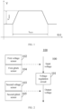
- FIG. 1 is a schematic structure diagram of a voltage attack type of an embodiment of the present application.
- attack strength V attack and attack duration t attack two characteristics of voltage attacks are defined, namely attack strength V attack and attack duration t attack . Accordingly, based on the characteristics of voltage attacks, voltage attacks are divided into a first type voltage attack and a second type voltage attack, where in the first type voltage attack, V attack is small and the t attack is large, and in the second type voltage attack, V attack is large and t attack is small.
- the first type voltage attack may be a supply voltage attack
- the second type voltage attack may be a glitch attack. Both the first type voltage attack and the second type voltage attack can make the circuit inside the chip work abnormally, causing a trigger to enter an error state and causing a processor to skip or perform a wrong operation, such that the security information in the chip is exposed.
- a voltage sensor may be configured for protection against the first type voltage attack, and a glitch sensor may be configured for protection against the second type voltage attack.
- a chip has a plurality of power domains (that is, internal supply).
- a voltage regulation circuit Voltage Regulator
- the chip contains a plurality such voltage regulation circuits, complex and diverse power domains are formed, and each power domain needs a voltage sensor and a glitch sensor to detect whether it is under voltage attack.
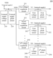
- FIG. 2 is a schematic structure diagram of the positional relationship between a voltage sensor and a glitch sensor and a voltage regulation circuit according to an embodiment of the present application.
- the voltage attack detection circuit 100 may include a voltage regulation circuit 101, a first voltage sensor 102, a second voltage sensor 103, a first glitch sensor 104 and a second glitch sensor 105.
- the first voltage sensor 102 and the first glitch sensor 104 are connected to an input terminal of the voltage regulation circuit 101
- the second voltage sensor 103 and the second glitch sensor 105 are connected to an output terminal of the voltage regulation circuit 101.
- the first voltage sensor 102 and the second voltage sensor 103 are configured to detect the input voltage and output voltage of the voltage regulation circuit 101 respectively, so as to detect whether the power domain where the voltage regulation circuit 101 is located is under voltage attack of the first voltage attack type.
- the first glitch sensor 104 and the second glitch sensor 105 are configured to detect the input voltage and output voltage of the voltage regulation circuit 101 respectively, to detect whether the power domain where the voltage regulation circuit 101 is located is under voltage attack of the second voltage attack type.
- FIG. 3 is a schematic structure diagram of a voltage attack detection circuit of an embodiment of the present application.
- the voltage attack detection circuit 200 may include at least one voltage regulation circuit.
- the at least one voltage regulation circuit may include a first voltage regulation circuit 231 and a second voltage regulation circuit 232, ..., and a N th voltage regulation circuit 23N, as shown in FIG. 3 .
- the at least one voltage regulation circuit is connected to an external supply (VDD), the at least one voltage regulation circuit is configured to convert the external supply to at least one internal supply respectively.
- the at least one internal supply may include internal supply V1, V2, ..., and VN shown in FIG. 3 , the at least one internal supply is configured to output at least one first voltage respectively for supplying power to one or some modules in the chip.
- the at least one first voltage may be partially equal, fully equal, or not equal to each other. This is not specifically limited in the embodiments of the present application.
- the voltage attack detection circuit 200 may further include a plurality of external supplies, in this case, each external supply of the plurality external supplies may be the external supply shown in FIG. 3 .
- the plurality of external supplies may be connected to a plurality of voltage regulation circuits respectively, and each voltage regulation circuit of the plurality of voltage regulation circuits is configured to convert the external supply connected thereto into the internal supply, the first voltage output by each voltage regulation circuit of the plurality of voltage regulation circuits may be connected to one voltage sensor and one glitch sensor, so that the first voltage sensor and the first glitch sensor perform the voltage attack detection, and accordingly, perform the attack protection in the whole power domain.
- the voltage attack detection circuit 200 may further include at least one voltage sensor.
- the voltage attack detection circuit 200 may include a first voltage sensor 241 and a second voltage sensor 242, ..., and a N th voltage sensor 24N as shown in FIG. 3 .
- the voltage attack detection circuit 200 may further include at least one glitch sensor; for example, the voltage attack detection circuit 200 may further include a first glitch sensor 251, a second glitch sensor 252,..., and a N th glitch sensor 25N as shown in FIG. 3 .
- the at least one voltage sensor is configured to receive the at least one first voltage respectively, and configured to output at least one first signal respectively
- the at least one first signal is configured to indicate whether the at least one internal supply is under voltage attack of a duration in a first range and an attack strength in a second range respectively
- the at least one glitch sensor is configured to receive the at least one first voltage respectively, and configured to output at least one second signal respectively
- the at least one second signal is configured to indicate whether the at least one internal supply is under voltage attack of a duration in a third range and an attack strength in a fourth range
- a minimum value of the first range is greater than or equal to a maximum value of the third range
- an absolute value of a maximum value of the second range is less than or equal to an absolute value of any value of the fourth range.
- a voltage attack with an attack duration in the first range and an attack strength in the second range can be detected, and through the at least one glitch sensor, a voltage attack with an attack duration in the third range and an attack strength in the fourth range can be detected, which can perform voltage attack protection in all aspects in terms of the attack duration and the attack strength, so as to improve the reliability of the voltage attack protection solution.
- the minimum value of the first range is 0.1 microsecond (us).
- the first range is 0.1us ⁇ + ⁇ , where the V attack may be a direct current voltage value, and the t attack is configured to indicate the duration of the voltage.
- the third range is 1 nanosecond (ns) to 0.1 microsecond (us).
- the second range is -0.5*V - 0.5*V, where V represents a voltage value of the external supply.
- the fourth range is 0.5*V - V, and/or the fourth range is -V - -0.5*V.
- first range the second range
- third range the fourth range
- fourth range a larger layout area and power consumption will be required, that is, when the glitch sensor is configured to detect a voltage attack with a shorter attack duration, it will require a smaller layout area and power consumption.
- third range and the fourth range based on the actual configuration of the glitch sensor or the actual requirements of the layout area and power consumption.
- those skilled in the art can also adjust the first range and the second range according to the actual configuration or actual requirements of the voltage sensor.
- the first range and the third range distinguished by 0.1 us, and the second range and the fourth range distinguished by ⁇ 0.5 ⁇ V shown in Table 1 are merely examples. This is not specifically limited in the embodiments of the present application.
- the absolute value of the maximum value of the second range and/or an absolute value of a minimum value of the fourth range is proportional to an absolute value of a voltage of the external supply.
- the absolute value of the maximum value of the second range and/or the absolute value of the minimum value of the fourth range may be a product of the absolute value of the voltage of the external supply and a preset percentage.
- the second range and the fourth range may be distinguished by 20% of the voltage of the external supply, that is, the second range is -0.2 ⁇ V ⁇ 0.2 ⁇ V.
- the fourth range is 0.2 ⁇ V ⁇ V, and/or the fourth range is -V ⁇ -0.2 ⁇ V.
- the at least one voltage sensor is connected to the at least one internal supply respectively, to receive the at least one first voltage respectively, and the at least one voltage sensor is configured to output the at least one first signal based on a received reference voltage and the at least one first voltage.
- each voltage sensor of the at least one voltage sensor may be configured to output a first signal component according to a received first voltage and a received first reference signal, the first signal component is configured to indicate whether the first voltage is greater than or equal to the first reference voltage, each voltage sensor of the at least one voltage sensor may further configured to output a second signal component according to the received first voltage and a received second reference voltage, and the second signal component may be configured to indicate whether the first voltage is less than or equal to the second reference voltage, where the first reference voltage is greater than the second reference voltage.
- the glitch sensor in embodiments of the present application may be any sensor that can be configured to detect the second type voltage attack.
- the glitch sensor may include a sensor of a latch.
- the voltage attack detection circuit further includes:
- a voltage sensor and a glitch sensor can be configured dedicatedly for the external supply.
- each voltage regulation circuit of the at least one voltage regulation circuit includes at least one of following elements: a low dropout regulator (LDO), a charge pump, a BUCK converter (BUCK), a Boost converter (Boost), and a bidirectional Direct current-Direct current converter (DC-DC converter), which can provide a voltage of stable output voltage.
- LDO low dropout regulator
- BUCK BUCK converter
- Boost Boost converter
- DC-DC converter bidirectional Direct current-Direct current converter
- each voltage sensor of the at least one voltage sensor includes a hysteresis comparator.
- FIGS. 1 to 3 are merely examples of the present application and may not be understood as limiting the present application
- the voltage attack detection circuit 200 may further include a reference voltage generation circuit, the reference voltage generation circuit is configured to generate a reference voltage, and the reference voltage generation circuit is connected to the at least one voltage sensor and the at least one glitch sensor respectively, so that each voltage senor of the at least one voltage sensor outputs a first signal based on the received reference voltage and the received first voltage, and each glitch sensor of the at least one glitch sensor outputs a second signal based on the received reference voltage and the received first voltage.
- the voltage attack detection circuit 200 may further include a reference voltage detection circuit, connected to the reference voltage generation circuit, for detecting whether the reference voltage is abnormal, and then generating an indication signal and outputting it to the at least one voltage sensor and the at least one glitch sensor.
- a reference voltage detection circuit connected to the reference voltage generation circuit, for detecting whether the reference voltage is abnormal, and then generating an indication signal and outputting it to the at least one voltage sensor and the at least one glitch sensor.
- the indication signal indicates that the reference voltage is abnormal, even if the at least one first signal is configured to indicate that the at least one internal supply is under attack of a duration in the first range and an attack strength in the second range, it is reset it to indicate that the at least one internal supply is not under voltage attack.
- the voltage attack circuit 200 may further include a glitch signal detection circuit, connected to the reference voltage generation circuit, to eliminate glitches on the reference voltage, thereby improving the accuracy of the indication signal.
- the present application is further provided with a chip, including a power management unit and the voltage attack detection circuit described above; where the power management unit is connected to the voltage attack detection circuit, and the voltage attack detection circuit is configured to detect whether a supply voltage of the power management unit is under voltage attack.
- the voltage attack detection circuit can be applied to any chip with a power management unit.
- a security chip for example, the security chip may be a fingerprint sensor chip or a processor chip, etc.
- the security chip is applicable for any kind of electronic device.
- portable or mobile computing devices such as smart-phones, laptops, tablets and game devices, and other electronic devices such as electronic databases, automobiles and bank automated teller machines (ATM).
- ATM bank automated teller machines
- the disclosed system, apparatus, and method may be implemented in other manners.
- the described apparatus embodiment is merely an example.
- the unit division is merely logical function division and may be other division in actual implementation.
- a plurality of units or components may be combined or integrated into another system, or some features may be ignored or not performed.
- the displayed or discussed mutual coupling or direct coupling or communication connection may be indirect coupling or communication connection via some interfaces, devices or units, and may be in electrical, mechanical or other forms.
- the units described as separate parts may be or may not be separated physically, and a component displayed as a unit may be or may not be a physical unit, namely, may be located in one place, or may be distributed on a plurality of network units. Part of or all of the units here may be selected according to a practical need to achieve the objectives of the solutions of the embodiments of the present application.
- functional units in the embodiments of the present disclosure may be integrated into one processing unit, or each of the units may exist alone physically, or two or more units are integrated into one unit.
- the functions When the functions are implemented in the form of a software functional unit and sold or used as an independent product, the functions may be stored in a computer-readable storage medium.
- the technical solution of the present application substantially, or the part of the present application making contribution to the prior art, or a part of the technical solution may be embodied in the form of a software product, and the computer software product is stored in a storage medium, which includes multiple instructions enabling computer equipment (which may be a personal computer, a server, network equipment or the like) to execute all of or part of the steps in the methods of the embodiments of the present application.
- the foregoing storage medium includes any medium that can store program code, such as a USB flash drive, a removable hard disk, a read-only memory (ROM), a random access memory (RAM), a magnetic disk, or an optical disc.
Landscapes
- Engineering & Computer Science (AREA)
- Physics & Mathematics (AREA)
- General Physics & Mathematics (AREA)
- General Engineering & Computer Science (AREA)
- Theoretical Computer Science (AREA)
- Computer Hardware Design (AREA)
- Power Engineering (AREA)
- Computer Security & Cryptography (AREA)
- Software Systems (AREA)
- Mathematical Physics (AREA)
- Measurement Of Current Or Voltage (AREA)
- Dc-Dc Converters (AREA)
- Power Sources (AREA)
Claims (11)
- Eine Schaltung zur Erkennung eines Spannungsangriffs (200), umfassend:mindestens eine Spannungsregelschaltung (101), wobei die mindestens eine Spannungsregelschaltung mit einer externen Versorgung verbunden ist, die mindestens eine Spannungsregelungsschaltung so konfiguriert ist, dass sie die externe Versorgung jeweils in mindestens eine interne Versorgung umwandelt, und die mindestens eine interne Versorgung so konfiguriert ist, dass sie jeweils mindestens eine erste Spannung ausgibt;mindestens einen Spannungssensor (102, 103) und mindestens einen Glitch-Sensor (104, 105), wobei jeder Spannungssensor in dem mindestens einen Spannungssensor so konfiguriert ist, dass er mit einer der mindestens einen Spannungsregelungsschaltung verbunden ist und so konfiguriert ist, dass er jeweils eine der mindestens einen ersten Spannung empfängt, und so konfiguriert ist, dass er jeweils mindestens ein erstes Signal ausgibt, wobei das mindestens eine erste Signal so konfiguriert ist, dass es anzeigt, ob die mindestens eine interne Versorgung einem Spannungsangriff mit einer Dauer innerhalb eines ersten Bereichs bzw. einer Angriffsstärke innerhalb eines zweiten Bereichs ausgesetzt ist, jeder Störungssensor in dem mindestens einen Störungssensor für eine der mindestens einen Spannungsregelungsschaltung konfiguriert ist und konfiguriert ist, jeweils eine der mindestens einen ersten Spannung zu empfangen, und konfiguriert ist, jeweils mindestens ein zweites Signal auszugeben, das mindestens eine zweite Signal so konfiguriert ist, dass es anzeigt, ob die mindestens eine interne Versorgung einem Spannungsangriff mit einer Dauer innerhalb eines dritten Bereichs bzw. einer Angriffsstärke innerhalb eines vierten Bereichs unterliegt, ein Minimalwert des ersten Bereichs größer als oder gleich einem Maximalwert des dritten Bereichs ist und ein Absolutwert eines Maximalwerts des zweiten Bereichs kleiner als oder gleich einem Absolutwert eines beliebigen Werts des vierten Bereichs ist.
- Schaltung zur Erkennung eines Spannungsangriffs (200) nach Anspruch 1, wobei der Mindestwert des ersten Bereichs 0,1 us beträgt.
- Schaltung zur Erkennung eines Spannungsangriffs (200) nach Anspruch 1 oder 2, wobei der dritte Bereich 1 ns bis 0,1 us beträgt.
- Schaltung zur Erkennung eines Spannungsangriffs (200) nach einem der Ansprüche 1 bis 3, wobei der Absolutwert des Maximalwerts des zweiten Bereichs und/oder ein Absolutwert eines Minimalwerts des vierten Bereichs proportional zu einem Absolutwert einer Spannung der externen Versorgung ist.
- Schaltung zur Erkennung eines Spannungsangriffs (200) nach Anspruch 4, wobei der zweite Bereich -0,5*V - 0,5*V beträgt, wobei V einen Spannungswert der externen Versorgung darstellt.
- Schaltung zur Erkennung eines Spannungsangriffs (200) nach Anspruch 4, wobei der vierte Bereich 0,5*V bis V ist und/oder der vierte Bereich -V - -0,5*V ist.
- Schaltung zur Erkennung eines Spannungsangriffs (200) nach einem der Ansprüche 1 bis 6, wobei der mindestens eine Spannungssensor jeweils mit der mindestens einen internen Versorgung verbunden ist, um jeweils die mindestens eine erste Spannung zu empfangen, und der mindestens eine Spannungssensor so konfiguriert ist, dass er das mindestens eine erste Signal auf der Grundlage einer empfangenen Spannungsreferenz und der mindestens einen ersten Spannung ausgibt.
- Schaltung zur Erkennung eines Spannungsangriffs (200) nach einem der Ansprüche 1 bis 7, wobei die Schaltung zur Erkennung eines Spannungsangriffs (200) weiterhin umfasst:einen Sensor für die externe Versorgungsspannung (210) und einen Glitch-Sensor für die externe Versorgung (220);wobei die externe Versorgung so konfiguriert ist, dass sie eine zweite Spannung ausgibt, der Sensor für die Spannung der externen Versorgung (210) mit der externen Versorgung verbunden ist, der Sensor für die Spannung der externen Versorgung (210) so konfiguriert ist, dass er die zweite Spannung empfängt und ein drittes Signal ausgibt, das dritte Signal so konfiguriert ist, dass es anzeigt, ob die zweite Spannung unter einem Spannungsangriff mit einer Dauer innerhalb des ersten Bereichs und einer Angriffsstärke innerhalb des zweiten Bereichs steht; der Glitch-Sensor für die externe Versorgung (220) mit der externen Versorgung verbunden ist, der Glitch-Sensor für die externe Versorgung (220) so konfiguriert ist, dass er die zweite Spannung empfängt und ein viertes Signal ausgibt, und das vierte Signal so konfiguriert ist, dass es anzeigt, ob die zweite Spannung unter einem Spannungsangriff mit einer Dauer innerhalb des dritten Bereichs und einer Angriffsstärke innerhalb des vierten Bereichs steht.
- Schaltung zur Erkennung eines Spannungsangriffs (200) nach einem der Ansprüche 1 bis 8, wobei jeder Spannungsregelkreis des mindestens einen Spannungsregelkreises mindestens eines der folgenden Elemente umfasst: einen Low-Dropout-Regler, eine Ladungspumpe, einen BUCK-Wandler, einen Boost-Wandler und einen bidirektionalen Gleichstrom-Gleichstrom-Wandler.
- Die Schaltung zur Erkennung eines Spannungsangriffs (200) nach einem der Ansprüche 1 bis 9, wobei jeder Spannungssensor des mindestens einen Spannungssensors einen Hysteresekomparator umfasst.
- Ein Chip, umfassend:eine Energieverwaltungseinheit; unddie Schaltung zur Erkennung eines Spannungsangriffs (200) nach einem der Ansprüche 1 bis 10;wobei die Leistungsverwaltungseinheit mit der Spannungsangriffserkennungsschaltung (200) verbunden ist und die Spannungsangriffserkennungsschaltung (200) so konfiguriert ist, dass sie erkennt, ob eine Versorgungsspannung der Leistungsverwaltungseinheit einem Spannungsangriff ausgesetzt ist.
Applications Claiming Priority (1)
| Application Number | Priority Date | Filing Date | Title |
|---|---|---|---|
| PCT/CN2020/082830 WO2021196094A1 (zh) | 2020-04-01 | 2020-04-01 | 电压攻击检测电路和芯片 |
Publications (3)
| Publication Number | Publication Date |
|---|---|
| EP3929602A1 EP3929602A1 (de) | 2021-12-29 |
| EP3929602A4 EP3929602A4 (de) | 2022-05-18 |
| EP3929602B1 true EP3929602B1 (de) | 2023-05-10 |
Family
ID=72075492
Family Applications (1)
| Application Number | Title | Priority Date | Filing Date |
|---|---|---|---|
| EP20924972.1A Active EP3929602B1 (de) | 2020-04-01 | 2020-04-01 | Schaltung und chip zur erfassung von spannungsabhängigem angriff |
Country Status (4)
| Country | Link |
|---|---|
| US (1) | US11940471B2 (de) |
| EP (1) | EP3929602B1 (de) |
| CN (1) | CN111566492B (de) |
| WO (1) | WO2021196094A1 (de) |
Families Citing this family (1)
| Publication number | Priority date | Publication date | Assignee | Title |
|---|---|---|---|---|
| CN114915397B (zh) * | 2022-04-25 | 2025-02-25 | 北京邮电大学 | 针对侧信道攻击的可同步精确电压毛刺注入电路及方法 |
Family Cites Families (13)
| Publication number | Priority date | Publication date | Assignee | Title |
|---|---|---|---|---|
| JP3863508B2 (ja) * | 2003-07-03 | 2006-12-27 | Necエレクトロニクス株式会社 | 電源電圧検出回路及び半導体集積回路装置 |
| EP2019996A1 (de) * | 2006-05-10 | 2009-02-04 | Nxp B.V. | Sensor mit einer schaltungs anordnung |
| US8988114B2 (en) * | 2012-11-20 | 2015-03-24 | Freescale Semiconductor, Inc. | Low-power voltage tamper detection |
| CN103034804B (zh) * | 2012-12-11 | 2015-12-23 | 深圳国微技术有限公司 | 安全芯片及其攻击检测电路 |
| US9523722B2 (en) * | 2014-06-02 | 2016-12-20 | Winbond Electronics Corporation | Method and apparatus for supply voltage glitch detection in a monolithic integrated circuit device |
| CN105629028B (zh) * | 2014-11-04 | 2019-03-01 | 华邦电子股份有限公司 | 检测电源电压突波方法以及单芯片集成电路装置 |
| CN105510688B (zh) * | 2016-01-25 | 2018-09-04 | 大唐微电子技术有限公司 | 一种实现cp测试的电压检测器 |
| US10156595B2 (en) * | 2016-12-09 | 2018-12-18 | Microsemi Soc Corp. | Power supply glitch detector |
| CN107505560B (zh) * | 2017-08-28 | 2019-09-06 | 北京银联金卡科技有限公司 | 芯片错误注入测试中的能量参数调整系统及方法 |
| CN107462827B (zh) * | 2017-08-31 | 2019-07-23 | 北京智芯微电子科技有限公司 | 带有内部稳压器的电源毛刺检测电路 |
| US12182260B2 (en) * | 2017-12-18 | 2024-12-31 | Nuvoton Technology Corporation | System and method for detecting fault injection attacks |
| US11074370B2 (en) * | 2018-03-09 | 2021-07-27 | Megachips Corporation | Information processing system, information processing device, and method for controlling information processing device |
| FR3107357B1 (fr) * | 2020-02-13 | 2022-03-04 | St Microelectronics Grenoble 2 | Détection de perturbations d'une alimentation électrique d'un circuit électronique |
-
2020
- 2020-04-01 EP EP20924972.1A patent/EP3929602B1/de active Active
- 2020-04-01 CN CN202080001158.4A patent/CN111566492B/zh active Active
- 2020-04-01 WO PCT/CN2020/082830 patent/WO2021196094A1/zh not_active Ceased
-
2021
- 2021-09-27 US US17/486,292 patent/US11940471B2/en active Active
Also Published As
| Publication number | Publication date |
|---|---|
| US11940471B2 (en) | 2024-03-26 |
| CN111566492A (zh) | 2020-08-21 |
| US20220011351A1 (en) | 2022-01-13 |
| EP3929602A4 (de) | 2022-05-18 |
| CN111566492B (zh) | 2022-02-11 |
| WO2021196094A1 (zh) | 2021-10-07 |
| EP3929602A1 (de) | 2021-12-29 |
Similar Documents
| Publication | Publication Date | Title |
|---|---|---|
| US12086294B2 (en) | Voltage attack detection circuit and chip | |
| EP3926349B1 (de) | Spannungsangriffdetektionsschaltung und -chip | |
| US11609277B2 (en) | Power glitch signal detection circuit and security chip | |
| US10164457B2 (en) | Charging method and apparatus | |
| US11181566B2 (en) | Detection circuit of electromagnetic fault injection and security chip | |
| US20130031381A1 (en) | Rack server system | |
| US20160179187A1 (en) | I/O Interface-Based Signal Output Method and Apparatus | |
| WO2022206646A1 (zh) | 电源芯片检测电路、电源芯片检测方法、装置和电子设备 | |
| Kim et al. | Eqz-ldo: A near-zero edp overhead,> 10m-attack-resilient, secure digital ldo featuring attack-detection and detection-driven protection for a correlation-power-analysis-resilient iot device | |
| CN112673263A (zh) | 毛刺信号检测电路、安全芯片和电子设备 | |
| US11940471B2 (en) | Voltage attack detection circuit and chip | |
| US7839127B2 (en) | Power supply circuit for motherboard | |
| US20160320820A1 (en) | Power excursion tolerant power system | |
| US20230115005A1 (en) | Flashing apparatus, booting and recovery appartus, and electronic device | |
| US20100066342A1 (en) | Control circuit for single chip ic | |
| CN217181045U (zh) | 一种供电电路、主板及电子设备 | |
| CN203180937U (zh) | 用于密码芯片的抗功耗分析攻击的稳压器、密码芯片 | |
| CN210091171U (zh) | 一种基于国产龙芯处理器的安全计算机 | |
| US7065662B2 (en) | Information handling system featuring a power-based current limiting circuit | |
| CN103023636A (zh) | 用于密码芯片的抗功耗分析攻击的稳压器、密码芯片 | |
| CN114765376A (zh) | 充电系统及电子设备 | |
| CN201868107U (zh) | 一种手持设备上的MicroSD卡供电系统结构 | |
| CN106155259A (zh) | 一种电源控制方法和装置 | |
| US20130271927A1 (en) | Mainboard having a reverse current blocking arrangement | |
| CN119621624A (zh) | Usb接口电路、线路板及设备 |
Legal Events
| Date | Code | Title | Description |
|---|---|---|---|
| STAA | Information on the status of an ep patent application or granted ep patent |
Free format text: STATUS: UNKNOWN |
|
| STAA | Information on the status of an ep patent application or granted ep patent |
Free format text: STATUS: THE INTERNATIONAL PUBLICATION HAS BEEN MADE |
|
| PUAI | Public reference made under article 153(3) epc to a published international application that has entered the european phase |
Free format text: ORIGINAL CODE: 0009012 |
|
| STAA | Information on the status of an ep patent application or granted ep patent |
Free format text: STATUS: REQUEST FOR EXAMINATION WAS MADE |
|
| 17P | Request for examination filed |
Effective date: 20210921 |
|
| AK | Designated contracting states |
Kind code of ref document: A1 Designated state(s): AL AT BE BG CH CY CZ DE DK EE ES FI FR GB GR HR HU IE IS IT LI LT LU LV MC MK MT NL NO PL PT RO RS SE SI SK SM TR |
|
| A4 | Supplementary search report drawn up and despatched |
Effective date: 20220420 |
|
| RIC1 | Information provided on ipc code assigned before grant |
Ipc: H01L 23/00 20060101ALI20220412BHEP Ipc: G06K 19/073 20060101ALI20220412BHEP Ipc: G06F 21/75 20130101ALI20220412BHEP Ipc: G01R 19/165 20060101ALI20220412BHEP Ipc: G01R 31/28 20060101AFI20220412BHEP |
|
| GRAP | Despatch of communication of intention to grant a patent |
Free format text: ORIGINAL CODE: EPIDOSNIGR1 |
|
| STAA | Information on the status of an ep patent application or granted ep patent |
Free format text: STATUS: GRANT OF PATENT IS INTENDED |
|
| DAV | Request for validation of the european patent (deleted) | ||
| DAX | Request for extension of the european patent (deleted) | ||
| INTG | Intention to grant announced |
Effective date: 20230215 |
|
| GRAS | Grant fee paid |
Free format text: ORIGINAL CODE: EPIDOSNIGR3 |
|
| GRAA | (expected) grant |
Free format text: ORIGINAL CODE: 0009210 |
|
| STAA | Information on the status of an ep patent application or granted ep patent |
Free format text: STATUS: THE PATENT HAS BEEN GRANTED |
|
| AK | Designated contracting states |
Kind code of ref document: B1 Designated state(s): AL AT BE BG CH CY CZ DE DK EE ES FI FR GB GR HR HU IE IS IT LI LT LU LV MC MK MT NL NO PL PT RO RS SE SI SK SM TR |
|
| REG | Reference to a national code |
Ref country code: GB Ref legal event code: FG4D |
|
| REG | Reference to a national code |
Ref country code: AT Ref legal event code: REF Ref document number: 1567199 Country of ref document: AT Kind code of ref document: T Effective date: 20230515 Ref country code: CH Ref legal event code: EP |
|
| REG | Reference to a national code |
Ref country code: DE Ref legal event code: R096 Ref document number: 602020010856 Country of ref document: DE |
|
| REG | Reference to a national code |
Ref country code: IE Ref legal event code: FG4D |
|
| REG | Reference to a national code |
Ref country code: LT Ref legal event code: MG9D |
|
| REG | Reference to a national code |
Ref country code: NL Ref legal event code: MP Effective date: 20230510 |
|
| REG | Reference to a national code |
Ref country code: AT Ref legal event code: MK05 Ref document number: 1567199 Country of ref document: AT Kind code of ref document: T Effective date: 20230510 |
|
| PG25 | Lapsed in a contracting state [announced via postgrant information from national office to epo] |
Ref country code: SE Free format text: LAPSE BECAUSE OF FAILURE TO SUBMIT A TRANSLATION OF THE DESCRIPTION OR TO PAY THE FEE WITHIN THE PRESCRIBED TIME-LIMIT Effective date: 20230510 Ref country code: PT Free format text: LAPSE BECAUSE OF FAILURE TO SUBMIT A TRANSLATION OF THE DESCRIPTION OR TO PAY THE FEE WITHIN THE PRESCRIBED TIME-LIMIT Effective date: 20230911 Ref country code: NO Free format text: LAPSE BECAUSE OF FAILURE TO SUBMIT A TRANSLATION OF THE DESCRIPTION OR TO PAY THE FEE WITHIN THE PRESCRIBED TIME-LIMIT Effective date: 20230810 Ref country code: NL Free format text: LAPSE BECAUSE OF FAILURE TO SUBMIT A TRANSLATION OF THE DESCRIPTION OR TO PAY THE FEE WITHIN THE PRESCRIBED TIME-LIMIT Effective date: 20230510 Ref country code: ES Free format text: LAPSE BECAUSE OF FAILURE TO SUBMIT A TRANSLATION OF THE DESCRIPTION OR TO PAY THE FEE WITHIN THE PRESCRIBED TIME-LIMIT Effective date: 20230510 Ref country code: AT Free format text: LAPSE BECAUSE OF FAILURE TO SUBMIT A TRANSLATION OF THE DESCRIPTION OR TO PAY THE FEE WITHIN THE PRESCRIBED TIME-LIMIT Effective date: 20230510 |
|
| PG25 | Lapsed in a contracting state [announced via postgrant information from national office to epo] |
Ref country code: RS Free format text: LAPSE BECAUSE OF FAILURE TO SUBMIT A TRANSLATION OF THE DESCRIPTION OR TO PAY THE FEE WITHIN THE PRESCRIBED TIME-LIMIT Effective date: 20230510 Ref country code: PL Free format text: LAPSE BECAUSE OF FAILURE TO SUBMIT A TRANSLATION OF THE DESCRIPTION OR TO PAY THE FEE WITHIN THE PRESCRIBED TIME-LIMIT Effective date: 20230510 Ref country code: LV Free format text: LAPSE BECAUSE OF FAILURE TO SUBMIT A TRANSLATION OF THE DESCRIPTION OR TO PAY THE FEE WITHIN THE PRESCRIBED TIME-LIMIT Effective date: 20230510 Ref country code: LT Free format text: LAPSE BECAUSE OF FAILURE TO SUBMIT A TRANSLATION OF THE DESCRIPTION OR TO PAY THE FEE WITHIN THE PRESCRIBED TIME-LIMIT Effective date: 20230510 Ref country code: IS Free format text: LAPSE BECAUSE OF FAILURE TO SUBMIT A TRANSLATION OF THE DESCRIPTION OR TO PAY THE FEE WITHIN THE PRESCRIBED TIME-LIMIT Effective date: 20230910 Ref country code: HR Free format text: LAPSE BECAUSE OF FAILURE TO SUBMIT A TRANSLATION OF THE DESCRIPTION OR TO PAY THE FEE WITHIN THE PRESCRIBED TIME-LIMIT Effective date: 20230510 Ref country code: GR Free format text: LAPSE BECAUSE OF FAILURE TO SUBMIT A TRANSLATION OF THE DESCRIPTION OR TO PAY THE FEE WITHIN THE PRESCRIBED TIME-LIMIT Effective date: 20230811 |
|
| PG25 | Lapsed in a contracting state [announced via postgrant information from national office to epo] |
Ref country code: FI Free format text: LAPSE BECAUSE OF FAILURE TO SUBMIT A TRANSLATION OF THE DESCRIPTION OR TO PAY THE FEE WITHIN THE PRESCRIBED TIME-LIMIT Effective date: 20230510 |
|
| PG25 | Lapsed in a contracting state [announced via postgrant information from national office to epo] |
Ref country code: SK Free format text: LAPSE BECAUSE OF FAILURE TO SUBMIT A TRANSLATION OF THE DESCRIPTION OR TO PAY THE FEE WITHIN THE PRESCRIBED TIME-LIMIT Effective date: 20230510 |
|
| PG25 | Lapsed in a contracting state [announced via postgrant information from national office to epo] |
Ref country code: SM Free format text: LAPSE BECAUSE OF FAILURE TO SUBMIT A TRANSLATION OF THE DESCRIPTION OR TO PAY THE FEE WITHIN THE PRESCRIBED TIME-LIMIT Effective date: 20230510 Ref country code: SK Free format text: LAPSE BECAUSE OF FAILURE TO SUBMIT A TRANSLATION OF THE DESCRIPTION OR TO PAY THE FEE WITHIN THE PRESCRIBED TIME-LIMIT Effective date: 20230510 Ref country code: RO Free format text: LAPSE BECAUSE OF FAILURE TO SUBMIT A TRANSLATION OF THE DESCRIPTION OR TO PAY THE FEE WITHIN THE PRESCRIBED TIME-LIMIT Effective date: 20230510 Ref country code: EE Free format text: LAPSE BECAUSE OF FAILURE TO SUBMIT A TRANSLATION OF THE DESCRIPTION OR TO PAY THE FEE WITHIN THE PRESCRIBED TIME-LIMIT Effective date: 20230510 Ref country code: DK Free format text: LAPSE BECAUSE OF FAILURE TO SUBMIT A TRANSLATION OF THE DESCRIPTION OR TO PAY THE FEE WITHIN THE PRESCRIBED TIME-LIMIT Effective date: 20230510 Ref country code: CZ Free format text: LAPSE BECAUSE OF FAILURE TO SUBMIT A TRANSLATION OF THE DESCRIPTION OR TO PAY THE FEE WITHIN THE PRESCRIBED TIME-LIMIT Effective date: 20230510 |
|
| REG | Reference to a national code |
Ref country code: DE Ref legal event code: R097 Ref document number: 602020010856 Country of ref document: DE |
|
| PLBE | No opposition filed within time limit |
Free format text: ORIGINAL CODE: 0009261 |
|
| STAA | Information on the status of an ep patent application or granted ep patent |
Free format text: STATUS: NO OPPOSITION FILED WITHIN TIME LIMIT |
|
| 26N | No opposition filed |
Effective date: 20240213 |
|
| PG25 | Lapsed in a contracting state [announced via postgrant information from national office to epo] |
Ref country code: SI Free format text: LAPSE BECAUSE OF FAILURE TO SUBMIT A TRANSLATION OF THE DESCRIPTION OR TO PAY THE FEE WITHIN THE PRESCRIBED TIME-LIMIT Effective date: 20230510 |
|
| PG25 | Lapsed in a contracting state [announced via postgrant information from national office to epo] |
Ref country code: SI Free format text: LAPSE BECAUSE OF FAILURE TO SUBMIT A TRANSLATION OF THE DESCRIPTION OR TO PAY THE FEE WITHIN THE PRESCRIBED TIME-LIMIT Effective date: 20230510 Ref country code: IT Free format text: LAPSE BECAUSE OF FAILURE TO SUBMIT A TRANSLATION OF THE DESCRIPTION OR TO PAY THE FEE WITHIN THE PRESCRIBED TIME-LIMIT Effective date: 20230510 |
|
| PG25 | Lapsed in a contracting state [announced via postgrant information from national office to epo] |
Ref country code: BG Free format text: LAPSE BECAUSE OF FAILURE TO SUBMIT A TRANSLATION OF THE DESCRIPTION OR TO PAY THE FEE WITHIN THE PRESCRIBED TIME-LIMIT Effective date: 20230510 |
|
| PG25 | Lapsed in a contracting state [announced via postgrant information from national office to epo] |
Ref country code: MC Free format text: LAPSE BECAUSE OF FAILURE TO SUBMIT A TRANSLATION OF THE DESCRIPTION OR TO PAY THE FEE WITHIN THE PRESCRIBED TIME-LIMIT Effective date: 20230510 |
|
| PG25 | Lapsed in a contracting state [announced via postgrant information from national office to epo] |
Ref country code: MC Free format text: LAPSE BECAUSE OF FAILURE TO SUBMIT A TRANSLATION OF THE DESCRIPTION OR TO PAY THE FEE WITHIN THE PRESCRIBED TIME-LIMIT Effective date: 20230510 Ref country code: BG Free format text: LAPSE BECAUSE OF FAILURE TO SUBMIT A TRANSLATION OF THE DESCRIPTION OR TO PAY THE FEE WITHIN THE PRESCRIBED TIME-LIMIT Effective date: 20230510 |
|
| REG | Reference to a national code |
Ref country code: CH Ref legal event code: PL |
|
| PG25 | Lapsed in a contracting state [announced via postgrant information from national office to epo] |
Ref country code: LU Free format text: LAPSE BECAUSE OF NON-PAYMENT OF DUE FEES Effective date: 20240401 |
|
| REG | Reference to a national code |
Ref country code: BE Ref legal event code: MM Effective date: 20240430 |
|
| PG25 | Lapsed in a contracting state [announced via postgrant information from national office to epo] |
Ref country code: LU Free format text: LAPSE BECAUSE OF NON-PAYMENT OF DUE FEES Effective date: 20240401 |
|
| PG25 | Lapsed in a contracting state [announced via postgrant information from national office to epo] |
Ref country code: BE Free format text: LAPSE BECAUSE OF NON-PAYMENT OF DUE FEES Effective date: 20240430 |
|
| PG25 | Lapsed in a contracting state [announced via postgrant information from national office to epo] |
Ref country code: BE Free format text: LAPSE BECAUSE OF NON-PAYMENT OF DUE FEES Effective date: 20240430 Ref country code: CH Free format text: LAPSE BECAUSE OF NON-PAYMENT OF DUE FEES Effective date: 20240430 |
|
| PG25 | Lapsed in a contracting state [announced via postgrant information from national office to epo] |
Ref country code: IE Free format text: LAPSE BECAUSE OF NON-PAYMENT OF DUE FEES Effective date: 20240401 |
|
| PG25 | Lapsed in a contracting state [announced via postgrant information from national office to epo] |
Ref country code: CY Free format text: LAPSE BECAUSE OF FAILURE TO SUBMIT A TRANSLATION OF THE DESCRIPTION OR TO PAY THE FEE WITHIN THE PRESCRIBED TIME-LIMIT; INVALID AB INITIO Effective date: 20200401 |
|
| PG25 | Lapsed in a contracting state [announced via postgrant information from national office to epo] |
Ref country code: HU Free format text: LAPSE BECAUSE OF FAILURE TO SUBMIT A TRANSLATION OF THE DESCRIPTION OR TO PAY THE FEE WITHIN THE PRESCRIBED TIME-LIMIT; INVALID AB INITIO Effective date: 20200401 |
|
| PG25 | Lapsed in a contracting state [announced via postgrant information from national office to epo] |
Ref country code: TR Free format text: LAPSE BECAUSE OF FAILURE TO SUBMIT A TRANSLATION OF THE DESCRIPTION OR TO PAY THE FEE WITHIN THE PRESCRIBED TIME-LIMIT Effective date: 20230510 |
|
| PGFP | Annual fee paid to national office [announced via postgrant information from national office to epo] |
Ref country code: GB Payment date: 20260325 Year of fee payment: 7 |
|
| PGFP | Annual fee paid to national office [announced via postgrant information from national office to epo] |
Ref country code: DE Payment date: 20260414 Year of fee payment: 7 |
|
| PGFP | Annual fee paid to national office [announced via postgrant information from national office to epo] |
Ref country code: FR Payment date: 20260408 Year of fee payment: 7 |