EP3926634A1 - Anti-fuse storage unit circuit and array circuit, and read/write method therefor - Google Patents
Anti-fuse storage unit circuit and array circuit, and read/write method therefor Download PDFInfo
- Publication number
- EP3926634A1 EP3926634A1 EP20869974.4A EP20869974A EP3926634A1 EP 3926634 A1 EP3926634 A1 EP 3926634A1 EP 20869974 A EP20869974 A EP 20869974A EP 3926634 A1 EP3926634 A1 EP 3926634A1
- Authority
- EP
- European Patent Office
- Prior art keywords
- unit
- switch
- terminal
- coupled
- module
- Prior art date
- Legal status (The legal status is an assumption and is not a legal conclusion. Google has not performed a legal analysis and makes no representation as to the accuracy of the status listed.)
- Granted
Links
Images


Classifications
-
- G—PHYSICS
- G11—INFORMATION STORAGE
- G11C—STATIC STORES
- G11C17/00—Read-only memories programmable only once; Semi-permanent stores, e.g. manually-replaceable information cards
- G11C17/14—Read-only memories programmable only once; Semi-permanent stores, e.g. manually-replaceable information cards in which contents are determined by selectively establishing, breaking or modifying connecting links by permanently altering the state of coupling elements, e.g. PROM
-
- G—PHYSICS
- G11—INFORMATION STORAGE
- G11C—STATIC STORES
- G11C17/00—Read-only memories programmable only once; Semi-permanent stores, e.g. manually-replaceable information cards
- G11C17/14—Read-only memories programmable only once; Semi-permanent stores, e.g. manually-replaceable information cards in which contents are determined by selectively establishing, breaking or modifying connecting links by permanently altering the state of coupling elements, e.g. PROM
- G11C17/16—Read-only memories programmable only once; Semi-permanent stores, e.g. manually-replaceable information cards in which contents are determined by selectively establishing, breaking or modifying connecting links by permanently altering the state of coupling elements, e.g. PROM using electrically-fusible links
-
- G—PHYSICS
- G11—INFORMATION STORAGE
- G11C—STATIC STORES
- G11C17/00—Read-only memories programmable only once; Semi-permanent stores, e.g. manually-replaceable information cards
- G11C17/06—Read-only memories programmable only once; Semi-permanent stores, e.g. manually-replaceable information cards using diode elements
-
- G—PHYSICS
- G11—INFORMATION STORAGE
- G11C—STATIC STORES
- G11C17/00—Read-only memories programmable only once; Semi-permanent stores, e.g. manually-replaceable information cards
- G11C17/14—Read-only memories programmable only once; Semi-permanent stores, e.g. manually-replaceable information cards in which contents are determined by selectively establishing, breaking or modifying connecting links by permanently altering the state of coupling elements, e.g. PROM
- G11C17/18—Auxiliary circuits, e.g. for writing into memory
Definitions
- the invention relates to the field of integrated circuits, in particular to an anti-fuse memory cell circuit, an array circuit and a reading and writing method thereof.
- OTP memory can store data in multiple OTP cells having two states of unprogrammed or programmed.
- An OTP unit may include a fuse or an anti-fuse, and once the fuse or the anti-fuse is programmed, the stored data is permanent. Because of this feature, OTP memory is used in various applications to store data.
- OTP is used to control the opening or closing of redundancy (redundancy) memory cells. For example, when a memory cell corresponding to a word line is defective, the corresponding OTP cell will be programmed (the output state of the OTP cell is changed from "0" to "1"), the DRAM control circuit will close the reading and writing of this memory unit, and open the reading and writing of a memory unit in the redundant area. At this time, the memory unit corresponding to the redundant area has fully replaced the defective memory unit, and thus the DRAM defects are repaired.
- the current one-time programmable memory has the following problems: 1. the one-time programmable memory device has a large static power consumption; 2. the one-time programmable memory readout circuit has poor reliability; 3. the one-time programmable memory control circuit is complicated; and 4. the one-time programmable memory device layout is not flexible.
- the problem to be solved by the present invention is to provide an anti-fuse memory cell circuit, an array circuit and a reading and writing method thereof, which have lower static power consumption, high reliability of the readout circuit, simple structure and flexible wiring.
- an anti-fuse memory cell circuit which includes:
- the anti-fuse device has a first end and a second end
- the switch module includes a first switch unit and a second switch unit, and both the first switch unit and the second switch unit have a first end, a second end and a control end, and the control ends are all coupled to the control module, the second ends are all coupled to the selection module, and the first end of the first switch unit is coupled to the inverter.
- the first end of the fuse device, and the first end of the second switch unit is coupled to the second end of the anti-fuse device.
- the switch module further includes a third switch unit.
- the third switch unit has a first end, a second end and a control end. The first end of the third switch unit is coupled to the anti-fuse device, the second end of the third switch unit is coupled to the ground signal, and the control end of the third switch unit is coupled to the control module.
- the selection module includes a bit line selection unit and a word line selection unit. Both the bit line selection unit and the word line selection unit have a first end, a second end and a control end.
- the control terminal is coupled to the bit line
- the first terminal of the bit line selection unit is coupled to the second terminal of the second switch unit
- the second terminal of the bit line selection unit is coupled to the ground signal
- the control end of the word line selection unit is coupled to the word line
- the first end of the word line selection unit is coupled to the second end of the first switch unit
- the second end of the word line selection unit is coupled to a power signal.
- the anti-fuse memory cell circuit further includes a current supply module having a first end and a second end. The first end of the current supply module is coupled to the power signal, and the second end is coupled to the second end of the word line select unit.
- control module includes a control unit, which control unit has an input terminal and an output terminal.
- the input terminal is coupled to the first terminal of the anti-fuse device, write enable signal, read enable signal, read delay signal is enabled, and the output terminal is coupled to the switch module.
- the control module further includes an amplifying unit having an input terminal and an output terminal.
- the input terminal is coupled to the first terminal of the anti-fuse device, and the output terminal is coupled to the input terminal of the control unit.
- the amplifying unit is used to amplify the signal of the first terminal of the anti-fuse device.
- control module includes a delay unit having an input terminal and an output terminal.
- the read enable signal is also coupled to the input terminal of the delay unit, and the output terminal of the delay unit is coupled to the control unit, and the delay unit is used to delay the read enable signal to form the read enable delay signal.
- the present invention also provides an anti-fuse memory cell array circuit, which includes:
- control module is a master control module, which is respectively coupled to the anti-fuse device and the switch module of each of the anti-fuse memory cell circuits.
- the master control module includes a control unit having an input terminal and an output terminal, and the input terminal is respectively coupled to the first of the anti-fuse device of each of the anti-fuse memory cell circuits.
- the output terminal is respectively coupled to the switch module of each of the anti-fuse memory cell circuits.
- the output terminal is a write enable signal, a read enable signal, and a read enable delay signal.
- the anti-fuse memory cell array circuit includes a plurality of the control modules, and one control module is coupled to at least the anti-fuse device and the switch module of one of the anti-fuse memory cell circuits.
- the anti-fuse memory cell array circuit further includes at least one current supply module, and at least some of the anti-fuse memory cell circuits share the same current supply module.
- the anti-fuse memory cell array circuit includes at least one word line selection unit, and at least some of the anti-fuse memory cell circuits share the same word line selection unit.
- the present invention also provides a method for reading and writing an anti-fuse memory cell circuit as described above, which includes:
- the selection module is turned on, in standby, the selection module is turned off, and in normal operation, the selection module is turned on.
- the anti-fuse device has a first end and a second end.
- the switch module includes a first switch unit and a second switch unit, and both the first switch unit and the second switch unit have a first end, a second end and a control end.
- the control ends are all coupled to the control module, the second ends are all coupled to the selection module, and the first end of the first switch unit is coupled to the inverter and a first end of a fuse device, and a first end of the second switch unit is coupled to a second end of the anti-fuse device.
- the first state of the switch module is when the first switch unit and the second switch unit are open.
- the second state of the switch module is when the first switch unit and the second switch unit are off.
- the third state of the switch module is: if the anti-fuse device is not broken down, the first switch unit is turned on and the second switch unit is turned off; if the anti-fuse device is broken down, then the first switch unit is closed, and the second switch unit is opened.
- the switch module includes a third switch unit.
- the third switch unit has a first end, a second end and a control end, and the first end of the third switch unit is coupled to the anti-fuse device, the second end of the third switch unit is coupled to a ground signal, and the control end of the third switch unit is coupled to the control module.
- the first state of the switch module is: the first switch unit and the second switch unit are open, and the third switch unit is closed.
- the second state of the switch module is: the first switch unit and the second switch unit are closed, and the third switch unit is open.
- the third state of the switch module is: if the anti-fuse device is not broken down, the control module controls the first switch unit to turn on, the second switch unit to turn off, and the third switch unit closed; if the anti-fuse device is broken down, the control module controls the first switching unit to close, the second switching unit to open, and the third switching unit to close.
- the anti-fuse memory unit circuit includes an anti-fuse device; a switch module, which is coupled to the anti-fuse device; a selection module, which is coupled to the switch module; a control module, which is respectively coupled to the anti-fuse device and the switch module, wherein the control module is used to switch the on-off mode of the switch module according to the breakdown state of the anti-fuse device.
- the anti-fuse memory unit circuit of the present invention can control the opening and closing of the switch module according to the output of the anti-fuse device (ie, the memory state of the anti-fuse memory unit), thereby achieving the purpose of saving power consumption.
- FIG. 1 is a circuit diagram of one embodiment of the anti-fuse memory cell circuit of the present invention. Please refer to FIG. 1 , the anti-fuse memory cell circuit includes an anti-fuse device C00, a switch module, a selection module, and a control module 12.
- the anti-fuse device C00 has a first end and a second end.
- the on-resistance is approximately 0 ohm; if the anti-fuse device C00 is not broken down, the on-resistance is approximately an infinite resistance. That is to say, the anti-fuse device C00 is non-conductive when it is not activated, but becomes a conductor after activation (breakdown), forming an electrical connection, and can selectively allow two devices or chips that are originally electrically isolated to make electrical connections and provide different resistance values for logic operations.
- the switch module is coupled to the anti-fuse device C00.
- the switch module includes a first switch unit MP2 and a second switch unit MN1.
- the first switch unit MP2 and the second switch unit MN1 each has a first terminal, a second terminal and a control terminal.
- the first switch unit MP2 is a P-type transistor and the second switch unit MN1 is an N-type transistor.
- the control ends of the first switch unit MP2 and the second switch unit MN1 are both coupled to the control module 12. Specifically, the control terminal of the first switch unit MP2 is coupled to the first control signal CTRL_A of the control module 12, and the control terminal of the second switch unit MN1 is coupled to the second control signal CTRL_B of the control module 12.
- the second ends of the first switch unit MP2 and the second switch unit MN1 are both coupled to a selection module. Specifically, the second end of the first switch unit MP2 is coupled to the word line selection unit MP1 of the selection module, and the second end of the second switch unit MN1 is coupled to the bit line of the selection module select cell MN2.
- the first end of the first switch unit MP2 is coupled to the first end of the anti-fuse device C00, and the first end of the second switch unit MN1 is coupled to the second end of the anti-fuse device C00.
- the readout circuit of the anti-fuse memory cell After the readout circuit of the anti-fuse memory cell reads the programming result, if the anti-fuse device C00 is broken down, the pull-up of the anti-fuse memory cell is turned off. If the anti-fuse device C00 is not broken, the pull-up of the anti-fuse memory cell is maintained. After the readout circuit of the anti-fuse memory cell reads the programming result, if the anti-fuse device C00 is broken down, the pull-down of the anti-fuse memory cell is maintained; if the anti-fuse device C00 is not broken down, then turn off the pull-down of the anti-fuse memory cell.
- the switch module further includes a third switch unit MN0, and the third switch unit MN0 has a first terminal, a second terminal, and a control terminal.
- the first end of the third switch unit MN0 is coupled to the first end of the anti-fuse device C00, the second end of the third switch unit MN0 is coupled to the ground signal, and the control terminal of the third switch unit MN0 is coupled to the third control signal CTRL_C of the control module 12.
- the third switch unit MN0 is an N-type transistor.
- the third switch unit MN0 is used to pull the first-level output node OUTA of the anti-fuse memory unit to ground when the one-time programmable memory cell is not working, and is also used to limit the first-level output node OUTA to initial working state when the one-time programmable memory cell is working.
- the selection module includes a bit line selection unit MN2 and a word line selection unit MP1. Both the bit line selection unit MN2 and the word line selection unit MP1 each has a first end, a second end and a control end.
- the bit line selection unit MN2 may be an N-type transistor
- the word line selection unit MP1 may be a P-type transistor.
- the control terminal of the bit line selection unit MN2 is coupled to the bit line BL00, the first terminal of the bit line selection unit MN2 is coupled to the second terminal of the second switch unit MN1, and the bit line selection unit MN2 the second end of is coupled to the ground signal.
- the control end of the word line selection unit MP1 is coupled to the word line WL00, the first end of the word line selection unit MP1 is coupled to the second end of the first switch unit MP2, and the word line selection unit MP1 The second end of is coupled to the power signal.
- bit line selection unit MN2 can control all the on-off of the anti-fuse memory cell and play a role in protecting the anti-fuse device C00.
- the anti-fuse memory cell circuit further includes a current supply module MP0, which has a first end and a second end, and the first end of the current supply module MP0 is coupled to the power signal, and the second end is coupled to all the second end of the word line selection unit MP1. That is, the second end of the word line selection unit MP1 is coupled to a power signal through the current supply module MP0.
- the current supply module MP0 is used as a mirror current source.
- the current supply module MP0 can control the magnitude of the current flowing through the anti-fuse device C00. In normal operation, the current supply module MP0 can control the anti-fuse device C00 in its pull-up capability. In this device, the current supply module MP0 can be a P-type transistor.
- the control module 12 includes a control unit 121, an amplification unit 122 and a delay unit 123.
- the control unit 121 is used to receive signals and output control signals.
- the control unit 121 has an input terminal and an output terminal.
- the input terminal is coupled to the first terminal of the anti-fuse device C00 through the amplifying unit 122, a write enable signal En_W, and a read enable signal En_R, and the read enable delay signal En_R_DLY.
- the output terminal is coupled to the switch module, and outputs a first control signal CTRL_A, a second control signal CTRL_B, and a third control signal CTRL_C.
- the first control signal CTRL_A is coupled to the control terminal of the first switch unit MP2
- the second control signal CTRL_B is coupled to the control terminal of the second switch unit MN1
- the third control signal CTRL_C is coupled to the control terminal of the third switch unit MN0.
- the amplifying unit 122 has an input terminal and an output terminal.
- the input terminal is coupled to the first-level output node OUTA of the anti-fuse device C00 for connecting the first-level output node OUTA of the anti-fuse device C00.
- the state amplification is the state of the secondary output OUTB, which can avoid logic errors in the subsequent digital circuits and improve the reliability of the readout circuit.
- the output terminal is coupled to the input terminal of the control unit 121 to input the secondary output OUTB of the anti-fuse device C00 to the input terminal of the control unit 121.
- the amplifying unit 122 is composed of two inverters.
- the delay unit 123 is used to generate the read enable delay signal En_R_DLY. Specifically, in addition to being coupled to the control unit 121, the read enable signal En_R is also coupled to the delay unit 123. The delay unit 123 delays the read enable signal En_R and then outputs the Read enable delay signal En_R_DLY.
- the delay unit 123 may be formed by connecting an even number of inverters in series, or the delay unit 123 may be an RC delay circuit.
- the delay time Td includes at least 4 inverter delays, and the amplifying unit 122 can amplify OUTA during Td period.
- the present invention also provides an exemplary implementation of the method for reading and writing the above anti-fuse memory cell circuit.
- Table 1 EN_W EN_R EN_R_DLY OUTA OUTB CTRL_A CTRL_B CTRL_C 1 0 0 X X 0 1 0 0 0 0 0 X X 1 0 1 0 1 0 1 0 X X 0 1 0 0 1 1 0 0 1 1 1 0 0 1 1 1 0 0 0 1 1 1 0 0 0 0 0 0 0 0 0 0 0 0 0 0 0 0 0 0 0 0 0 0 0 0 0 0
- the method of programming is that the control module controls the switch module to be in the first state to perform a write operation on the anti-fuse device. Examples are as follows:
- the standby method is that the control module controls the switch module to be in the second state so as to reduce the power consumption of the anti-fuse device. Examples are as follows:
- control module controls the switch module to be in the third state to perform a read operation on the anti-fuse device. Examples are as follows:
- the first P-type transistor MP0, the first selection transistor MP1 and the first switch tube MP2 will pull OUTA up to "1"; if the anti-fuse device C00 is broken down, the on-resistance of the anti-fuse device C00 is approximately 0 ohm, and the second switch tube MN1 and the second selection transistor MN2 will keep OUTA at "0". 3.
- the anti-fuse memory unit circuit of the present invention is a pure combinational circuit. Compared with a time sequential circuit, all paths are closed after the Td delay, and the whole circuit has stopped any logic action, leading to lower static power consumption, at approximately zero power consumption.
- the inventive anti-fuse memory cell circuit essentially forms two positive feedback loops through the design of switches and logic operation modules so that the readout circuit can read "0" or "1" more reliably; at the same time, the present inventive anti-fuse memory unit circuit can save the complicated timing sequence control part, and even can output the OUTA/OUTB of the readout circuit directly as the code output of the anti-fuse device without latching it.
- the internal code structure of the logic operation unit LOGIC circuit is as follows:
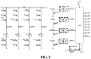
- FIG. 2 is a circuit diagram of the first exemplary embodiment of the anti-fuse memory array circuit. Please refer to FIG. 2 .
- the anti-fuse memory array circuit includes at least one control module and a plurality of anti-fuse memory cell circuits.
- the anti-fuse memory unit circuit includes: an anti-fuse device, a switch module, and a selection module.
- the anti-fuse device, switch module, and selection module are the same as the anti-fuse device, switch module, and switch module of the anti-fuse memory unit circuit.
- the selection module structure is the same.
- the control module is respectively coupled to the anti-fuse device and the switch module of the anti-fuse memory unit circuit, and the control module is configured to switch on-off mode of the switch module of the anti-fuse device, according to the breakdown state of the anti-fuse device,.
- control module is a master control module, which is respectively coupled to the anti-fuse memory device and the switch module of each of the anti-fuse memory unit circuits.
- the overall control module includes a control unit 121, the input of the control unit is coupled to the write enable signal EN_W, read enable signal EN_R, and read enable delay signal EN_R_DLY and each of the first end of the anti-fuse device C00. That is, the anti-fuse memory cell circuit shares the write enable signal EN_W, the read enable signal EN_R, and the read enable delay signal EN_R_DLY to reduce the number of input lines, thereby reducing the area.
- control unit outputs a control signal
- control signal is coupled to the third switch unit MN0 of the anti-fuse memory unit, that is, the anti-fuse memory unit circuit shares the control unit.
- the third control signal CTRL_C is used to reduce the number of control lines, thereby reducing the area.
- the internal pure combinational logic can continue to be optimized to reduce the number of logic gates, thereby reducing the area.
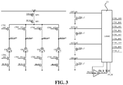
- FIG. 3 is a circuit diagram of a second exemplary embodiment of the anti-fuse memory array circuit.
- the difference between the second embodiment and the first embodiment is that the anti-fuse memory array circuit further includes at least one current supply module MP0, and at least part of the anti-fuse memory unit circuits share the current supply module MP0.
- the anti-fuse memory array circuit further includes at least one current supply module MP0, and at least part of the anti-fuse memory unit circuits share the current supply module MP0.
- all the anti-fuse memory cell circuits share one current supply module MP0.
- the current supply module MP0 acts as a current mirror to provide current and limit current, and the anti-fuse memory unit circuits share the current supply module MP0 to reduce the number of transistors and thereby reduce the occupying area.
- the anti-fuse memory array circuit further includes at least one word line selection unit MP1, and at least part of the anti-fuse memory cell circuits share the word line selection unit MP1, for example, all of the anti-fuse memory cell circuits share the word line selection cell MP1.
- the word line selection unit MP1 is a selection transistor controlled by a word line, and the word line selection unit MP1 shared by the anti-fuse memory unit circuit can reduce the number of transistors, thereby reducing the area.
- FIG. 4 is a circuit diagram of a third exemplary embodiment of the anti-fuse memory unit array circuits.
- the control module includes an amplifying unit 122 which is composed of two inverters, wherein the amplifying unit 122 can be combined with the control unit 121.
- the circuits are combined to reduce the number of logic gates, thereby reducing the occupying area.
- the function of the amplifying unit 122 is realized by the control unit 121.
Landscapes
- Read Only Memory (AREA)
- Static Random-Access Memory (AREA)
Abstract
Description
- This application claims the benefit of priority to CN Patent Application
CN 201910931356.X filed on 09/29/2019 - The invention relates to the field of integrated circuits, in particular to an anti-fuse memory cell circuit, an array circuit and a reading and writing method thereof.
- One Time Programmable (OTP) memory can store data in multiple OTP cells having two states of unprogrammed or programmed. An OTP unit may include a fuse or an anti-fuse, and once the fuse or the anti-fuse is programmed, the stored data is permanent. Because of this feature, OTP memory is used in various applications to store data. In DRAM, OTP is used to control the opening or closing of redundancy (redundancy) memory cells. For example, when a memory cell corresponding to a word line is defective, the corresponding OTP cell will be programmed (the output state of the OTP cell is changed from "0" to "1"), the DRAM control circuit will close the reading and writing of this memory unit, and open the reading and writing of a memory unit in the redundant area. At this time, the memory unit corresponding to the redundant area has fully replaced the defective memory unit, and thus the DRAM defects are repaired.
- The current one-time programmable memory has the following problems: 1. the one-time programmable memory device has a large static power consumption; 2. the one-time programmable memory readout circuit has poor reliability; 3. the one-time programmable memory control circuit is complicated; and 4. the one-time programmable memory device layout is not flexible.
- Therefore, how to overcome the above-mentioned problems has become an urgent technical problem to be solved at present.
- The problem to be solved by the present invention is to provide an anti-fuse memory cell circuit, an array circuit and a reading and writing method thereof, which have lower static power consumption, high reliability of the readout circuit, simple structure and flexible wiring.
- In order to solve the above problem, the present invention provides an anti-fuse memory cell circuit which includes:
- anti-fuse device;
- a switch module, coupled to the anti-fuse device;
- a selection module, coupled to the switch module;
- control modules, respectively coupled to the anti-fuse device and the switch module;
- wherein, the control module is configured to switch the on-off mode of the switch module according to the breakdown state of the anti-fuse device.
- Further, the anti-fuse device has a first end and a second end, the switch module includes a first switch unit and a second switch unit, and both the first switch unit and the second switch unit have a first end, a second end and a control end, and the control ends are all coupled to the control module, the second ends are all coupled to the selection module, and the first end of the first switch unit is coupled to the inverter. The first end of the fuse device, and the first end of the second switch unit is coupled to the second end of the anti-fuse device.
- Further, the switch module further includes a third switch unit. The third switch unit has a first end, a second end and a control end. The first end of the third switch unit is coupled to the anti-fuse device, the second end of the third switch unit is coupled to the ground signal, and the control end of the third switch unit is coupled to the control module.
- Further, the selection module includes a bit line selection unit and a word line selection unit. Both the bit line selection unit and the word line selection unit have a first end, a second end and a control end. The control terminal is coupled to the bit line, the first terminal of the bit line selection unit is coupled to the second terminal of the second switch unit, the second terminal of the bit line selection unit is coupled to the ground signal, the control end of the word line selection unit is coupled to the word line, the first end of the word line selection unit is coupled to the second end of the first switch unit, and the second end of the word line selection unit is coupled to a power signal.
- Further, the anti-fuse memory cell circuit further includes a current supply module having a first end and a second end. The first end of the current supply module is coupled to the power signal, and the second end is coupled to the second end of the word line select unit.
- Further, the control module includes a control unit, which control unit has an input terminal and an output terminal. The input terminal is coupled to the first terminal of the anti-fuse device, write enable signal, read enable signal, read delay signal is enabled, and the output terminal is coupled to the switch module.
- The control module further includes an amplifying unit having an input terminal and an output terminal. The input terminal is coupled to the first terminal of the anti-fuse device, and the output terminal is coupled to the input terminal of the control unit. The amplifying unit is used to amplify the signal of the first terminal of the anti-fuse device.
- Further, the control module includes a delay unit having an input terminal and an output terminal. The read enable signal is also coupled to the input terminal of the delay unit, and the output terminal of the delay unit is coupled to the control unit, and the delay unit is used to delay the read enable signal to form the read enable delay signal.
- The present invention also provides an anti-fuse memory cell array circuit, which includes:
- at least one control module;
- at least one anti-fuse memory cell circuit, the anti-fuse memory cell circuit includes:
- an anti-fuse device;
- a switch module, coupled to the anti-fuse device;
- a selection module, coupled to the switch module;
- here the control module is respectively coupled to the anti-fuse device and the switch module of the anti-fuse memory cell circuit, and the control module is configured to switch the on-off anti-fuse device mode according to the breakdown state of the anti-fuse device.
- Further, the control module is a master control module, which is respectively coupled to the anti-fuse device and the switch module of each of the anti-fuse memory cell circuits.
- Further, the master control module includes a control unit having an input terminal and an output terminal, and the input terminal is respectively coupled to the first of the anti-fuse device of each of the anti-fuse memory cell circuits. The output terminal is respectively coupled to the switch module of each of the anti-fuse memory cell circuits. The output terminal is a write enable signal, a read enable signal, and a read enable delay signal.
- Further, the anti-fuse memory cell array circuit includes a plurality of the control modules, and one control module is coupled to at least the anti-fuse device and the switch module of one of the anti-fuse memory cell circuits.
- Further, the anti-fuse memory cell array circuit further includes at least one current supply module, and at least some of the anti-fuse memory cell circuits share the same current supply module.
- Further, the anti-fuse memory cell array circuit includes at least one word line selection unit, and at least some of the anti-fuse memory cell circuits share the same word line selection unit.
- The present invention also provides a method for reading and writing an anti-fuse memory cell circuit as described above, which includes:
- during programming: the control module controls the switch module to be in the first state to perform a write operation on the anti-fuse device;
- in standby: the control module controls the switch module to be in the second state to reduce the power consumption of the anti-fuse device;
- during normal operation: the control module controls the switch module to be in the third state to perform a read operation on the anti-fuse device.
- Further, during programming, the selection module is turned on, in standby, the selection module is turned off, and in normal operation, the selection module is turned on.
- Further, the anti-fuse device has a first end and a second end. The switch module includes a first switch unit and a second switch unit, and both the first switch unit and the second switch unit have a first end, a second end and a control end. The control ends are all coupled to the control module, the second ends are all coupled to the selection module, and the first end of the first switch unit is coupled to the inverter and a first end of a fuse device, and a first end of the second switch unit is coupled to a second end of the anti-fuse device.
- The first state of the switch module is when the first switch unit and the second switch unit are open.
- The second state of the switch module is when the first switch unit and the second switch unit are off.
- The third state of the switch module is: if the anti-fuse device is not broken down, the first switch unit is turned on and the second switch unit is turned off; if the anti-fuse device is broken down, then the first switch unit is closed, and the second switch unit is opened.
- Further, the switch module includes a third switch unit. The third switch unit has a first end, a second end and a control end, and the first end of the third switch unit is coupled to the anti-fuse device, the second end of the third switch unit is coupled to a ground signal, and the control end of the third switch unit is coupled to the control module.
- The first state of the switch module is: the first switch unit and the second switch unit are open, and the third switch unit is closed.
- The second state of the switch module is: the first switch unit and the second switch unit are closed, and the third switch unit is open.
- The third state of the switch module is: if the anti-fuse device is not broken down, the control module controls the first switch unit to turn on, the second switch unit to turn off, and the third switch unit closed; if the anti-fuse device is broken down, the control module controls the first switching unit to close, the second switching unit to open, and the third switching unit to close.
- The advantages of the present invention are:
- 1. The anti-fuse memory cell circuit is a pure combinational circuit. Compared with a time sequence circuit, after a delay of a certain time, after the read and write operation is completed, all paths are closed, and the entire circuit stops logic action, and the static power consumption is even lower to approximately 0.
- 2. The anti-fuse memory cell circuit o essentially forms two positive feedback loops through the design of switches and logic operation modules, so that the readout circuit can read "0" or "1" more reliably.
- 3. The anti-fuse memory unit circuit can save complicated timing control parts, and even the output OUTA/OUTB of the readout circuit can be directly used as the code output of the anti-fuse without being latched.
- 4. The circuit layout of the anti-fuse memory cell is flexible.
-
-
FIG. 1 is a circuit diagram of a specific embodiment of the anti-fuse memory cell circuit of the present invention. -
FIG. 2 is a circuit diagram of a first specific embodiment of an anti-fuse memory array circuit. -
Fig. 3 is a circuit diagram of a second specific embodiment of an anti-fuse memory array circuit. -
FIG. 4 is a circuit diagram of a third specific embodiment of the anti-fuse memory array circuit. - The specific implementations of the anti-fuse memory cell circuit, the array circuit and the reading and writing method thereof provided by the present invention will be described in detail below with reference to the accompanying drawings.
- The anti-fuse memory unit circuit includes an anti-fuse device; a switch module, which is coupled to the anti-fuse device; a selection module, which is coupled to the switch module; a control module, which is respectively coupled to the anti-fuse device and the switch module, wherein the control module is used to switch the on-off mode of the switch module according to the breakdown state of the anti-fuse device. The anti-fuse memory unit circuit of the present invention can control the opening and closing of the switch module according to the output of the anti-fuse device (ie, the memory state of the anti-fuse memory unit), thereby achieving the purpose of saving power consumption.
FIG. 1 is a circuit diagram of one embodiment of the anti-fuse memory cell circuit of the present invention. Please refer toFIG. 1 , the anti-fuse memory cell circuit includes an anti-fuse device C00, a switch module, a selection module, and acontrol module 12. - The anti-fuse device C00 has a first end and a second end. During programming, if the anti-fuse device C00 is broken down, the on-resistance is approximately 0 ohm; if the anti-fuse device C00 is not broken down, the on-resistance is approximately an infinite resistance. That is to say, the anti-fuse device C00 is non-conductive when it is not activated, but becomes a conductor after activation (breakdown), forming an electrical connection, and can selectively allow two devices or chips that are originally electrically isolated to make electrical connections and provide different resistance values for logic operations.
- The switch module is coupled to the anti-fuse device C00. The switch module includes a first switch unit MP2 and a second switch unit MN1. The first switch unit MP2 and the second switch unit MN1 each has a first terminal, a second terminal and a control terminal. In this exemplary embodiment, the first switch unit MP2 is a P-type transistor and the second switch unit MN1 is an N-type transistor.
- The control ends of the first switch unit MP2 and the second switch unit MN1 are both coupled to the
control module 12. Specifically, the control terminal of the first switch unit MP2 is coupled to the first control signal CTRL_A of thecontrol module 12, and the control terminal of the second switch unit MN1 is coupled to the second control signal CTRL_B of thecontrol module 12. - The second ends of the first switch unit MP2 and the second switch unit MN1 are both coupled to a selection module. Specifically, the second end of the first switch unit MP2 is coupled to the word line selection unit MP1 of the selection module, and the second end of the second switch unit MN1 is coupled to the bit line of the selection module select cell MN2.
- The first end of the first switch unit MP2 is coupled to the first end of the anti-fuse device C00, and the first end of the second switch unit MN1 is coupled to the second end of the anti-fuse device C00.
- After the readout circuit of the anti-fuse memory cell reads the programming result, if the anti-fuse device C00 is broken down, the pull-up of the anti-fuse memory cell is turned off. If the anti-fuse device C00 is not broken, the pull-up of the anti-fuse memory cell is maintained. After the readout circuit of the anti-fuse memory cell reads the programming result, if the anti-fuse device C00 is broken down, the pull-down of the anti-fuse memory cell is maintained; if the anti-fuse device C00 is not broken down, then turn off the pull-down of the anti-fuse memory cell.
- Further, the switch module further includes a third switch unit MN0, and the third switch unit MN0 has a first terminal, a second terminal, and a control terminal. The first end of the third switch unit MN0 is coupled to the first end of the anti-fuse device C00, the second end of the third switch unit MN0 is coupled to the ground signal, and the control terminal of the third switch unit MN0 is coupled to the third control signal CTRL_C of the
control module 12. In this embodiment, the third switch unit MN0 is an N-type transistor. The third switch unit MN0 is used to pull the first-level output node OUTA of the anti-fuse memory unit to ground when the one-time programmable memory cell is not working, and is also used to limit the first-level output node OUTA to initial working state when the one-time programmable memory cell is working. - The selection module includes a bit line selection unit MN2 and a word line selection unit MP1. Both the bit line selection unit MN2 and the word line selection unit MP1 each has a first end, a second end and a control end. Herein, the bit line selection unit MN2 may be an N-type transistor, and the word line selection unit MP1 may be a P-type transistor.
- The control terminal of the bit line selection unit MN2 is coupled to the bit line BL00, the first terminal of the bit line selection unit MN2 is coupled to the second terminal of the second switch unit MN1, and the bit line selection unit MN2 the second end of is coupled to the ground signal. The control end of the word line selection unit MP1 is coupled to the word line WL00, the first end of the word line selection unit MP1 is coupled to the second end of the first switch unit MP2, and the word line selection unit MP1 The second end of is coupled to the power signal.
- During programming, the bit line selection unit MN2 can control all the on-off of the anti-fuse memory cell and play a role in protecting the anti-fuse device C00.
- Further, the anti-fuse memory cell circuit further includes a current supply module MP0, which has a first end and a second end, and the first end of the current supply module MP0 is coupled to the power signal, and the second end is coupled to all the second end of the word line selection unit MP1. That is, the second end of the word line selection unit MP1 is coupled to a power signal through the current supply module MP0. The current supply module MP0 is used as a mirror current source. During programming, the current supply module MP0 can control the magnitude of the current flowing through the anti-fuse device C00. In normal operation, the current supply module MP0 can control the anti-fuse device C00 in its pull-up capability. In this device, the current supply module MP0 can be a P-type transistor.
- The
control module 12 includes acontrol unit 121, anamplification unit 122 and adelay unit 123. - The
control unit 121 is used to receive signals and output control signals. Exemplarily, thecontrol unit 121 has an input terminal and an output terminal. The input terminal is coupled to the first terminal of the anti-fuse device C00 through the amplifyingunit 122, a write enable signal En_W, and a read enable signal En_R, and the read enable delay signal En_R_DLY. The output terminal is coupled to the switch module, and outputs a first control signal CTRL_A, a second control signal CTRL_B, and a third control signal CTRL_C. The first control signal CTRL_A is coupled to the control terminal of the first switch unit MP2, the second control signal CTRL_B is coupled to the control terminal of the second switch unit MN1, and the third control signal CTRL_C is coupled to the control terminal of the third switch unit MN0. - The amplifying
unit 122 has an input terminal and an output terminal. The input terminal is coupled to the first-level output node OUTA of the anti-fuse device C00 for connecting the first-level output node OUTA of the anti-fuse device C00. The state amplification is the state of the secondary output OUTB, which can avoid logic errors in the subsequent digital circuits and improve the reliability of the readout circuit. The output terminal is coupled to the input terminal of thecontrol unit 121 to input the secondary output OUTB of the anti-fuse device C00 to the input terminal of thecontrol unit 121. In this exemplary implementation, the amplifyingunit 122 is composed of two inverters. - The
delay unit 123 is used to generate the read enable delay signal En_R_DLY. Specifically, in addition to being coupled to thecontrol unit 121, the read enable signal En_R is also coupled to thedelay unit 123. Thedelay unit 123 delays the read enable signal En_R and then outputs the Read enable delay signal En_R_DLY. Thedelay unit 123 may be formed by connecting an even number of inverters in series, or thedelay unit 123 may be an RC delay circuit. The delay time Td includes at least 4 inverter delays, and the amplifyingunit 122 can amplify OUTA during Td period. - The present invention also provides an exemplary implementation of the method for reading and writing the above anti-fuse memory cell circuit. Please refer to Table 1:
Table 1 EN_W EN_R EN_R_DLY OUTA OUTB CTRL_A CTRL_B CTRL_C 1 0 0 X X 0 1 0 0 0 0 X X 1 0 1 0 1 0 X X 0 1 0 0 1 1 0 0 1 1 0 0 1 1 1 1 0 0 0 - The method of programming is that the control module controls the switch module to be in the first state to perform a write operation on the anti-fuse device. Examples are as follows:
- When the write enable signal EN_W=1 and the read enable signal EN_R=0, the first control signal CTRL A=O (the first switch tube MP2 is turned on) and the second control signal CTRL_B=1 (the second switch tube MN1 is turned on)), the third control signal CTRL C=O (the third switch tube MN0 is turned off), VDD is a high voltage; if the word line WL00 is "0" and the bit line BL00 is "1", then the anti-fuse device C00 breaks down. In other cases, the anti-fuse device C00 has not been broken down, then the on-resistance is approximately infinite ohms.
- The standby method is that the control module controls the switch module to be in the second state so as to reduce the power consumption of the anti-fuse device. Examples are as follows:
- When the write enable signal EN_W=0 and the read enable signal EN_R=0, the first control signal CTRL_A=1 (the first switch tube MP2 is turned off) and the second control signal CTRL B=O (the second switch tube MN1 is turned off)), the third control signal CTRL_C=1 (the third switch tube MN0 is turned on), and VDD is the normal voltage. At this time the static power consumption of the anti-fuse memory cell is approximately 0, and the default output of OUTB is "0".
- The method during normal operation is that the control module controls the switch module to be in the third state to perform a read operation on the anti-fuse device. Examples are as follows:
- 1. When word line WL00=0, bit line BL00=1, VDD is the normal voltage, write enable signal EN_W=0, read enable signal EN_R=0, read enable delay signal EN_R_DLY=0, then the first control signal CTRL_A=1 (the first switch tube MP2 is turned off), the second control signal CTRL B=O (the second switch tube MN1 is turned off), and the third control signal CTRL_C=1 (the third switch tube MN0 is turned on). 2. When word line WL00=0, bit line BL00=1, VDD is the normal voltage, write enable signal EN_W=0, read enable signal EN_R=1, read enable delay signal EN_R_DLY=0, then the first control signal CTRL A=O (the first switch tube MP2 is turned on), the second control signal CTRL_B=1 (the second switch tube MN1 is turned on), and the third control signal CTRL_C=0 (the third switch tube MN0 is turned off); if the anti-fuse device C00 is not broken down, the on-resistance of the anti-fuse device C00 is approximately infinite ohms. The first P-type transistor MP0, the first selection transistor MP1 and the first switch tube MP2 will pull OUTA up to "1"; if the anti-fuse device C00 is broken down, the on-resistance of the anti-fuse device C00 is approximately 0 ohm, and the second switch tube MN1 and the second selection transistor MN2 will keep OUTA at "0". 3. When word line WL00=0, bit line BL00=1, VDD is the normal voltage, write enable signal EN_W=0, read enable signal EN_R=1, read enable delay signal EN_R_DLY=, if OUTB=OUTA= 1, the first control signal CTRL A=O (the first switch tube MP2 is turned on), the second control signal CTRL B=O (the second switch tube MN1 is turned off), and the third control signal CTRL_C=0 (the third switch tube MN0 is turned off) ; If OUTB=OUTA=0, the first control signal CTRL_A=1 (the first switch tube MP2 is turned off), the second control signal CTRL_B=1 (the second switch tube MN1 is turned on), and the third control signal CTRL_C=0 (the third switch tube MN0 is closed).
- The anti-fuse memory unit circuit of the present invention is a pure combinational circuit. Compared with a time sequential circuit, all paths are closed after the Td delay, and the whole circuit has stopped any logic action, leading to lower static power consumption, at approximately zero power consumption. The inventive anti-fuse memory cell circuit essentially forms two positive feedback loops through the design of switches and logic operation modules so that the readout circuit can read "0" or "1" more reliably; at the same time, the present inventive anti-fuse memory unit circuit can save the complicated timing sequence control part, and even can output the OUTA/OUTB of the readout circuit directly as the code output of the anti-fuse device without latching it.
- Further, to realize the control of the anti-fuse memory unit circuit of the present invention, the internal code structure of the logic operation unit LOGIC circuit is as follows:
- CTRL_A = (!EN_W) && ( (!EN_R) && (!EN_R_DLY) || EN_R && EN_R_DLY && (!OUTB) )
- CTRL_B = EN_W && ( !EN_R) && (!EN_R_DLY) || (!EN_W) && EN_R && ((!EN_R_DLY) || EN_R_DLY && (!OUTB) )
- CTRL_C = (!EN_W) && (!EN_R)
- The present invention also provides a first specific implementation of the anti-fuse memory array circuit.
FIG. 2 is a circuit diagram of the first exemplary embodiment of the anti-fuse memory array circuit. Please refer toFIG. 2 . The anti-fuse memory array circuit includes at least one control module and a plurality of anti-fuse memory cell circuits. The anti-fuse memory unit circuit includes: an anti-fuse device, a switch module, and a selection module. The anti-fuse device, switch module, and selection module are the same as the anti-fuse device, switch module, and switch module of the anti-fuse memory unit circuit. The selection module structure is the same. The control module is respectively coupled to the anti-fuse device and the switch module of the anti-fuse memory unit circuit, and the control module is configured to switch on-off mode of the switch module of the anti-fuse device, according to the breakdown state of the anti-fuse device,. - In this embodiment, the control module is a master control module, which is respectively coupled to the anti-fuse memory device and the switch module of each of the anti-fuse memory unit circuits. The overall control module includes a
control unit 121, the input of the control unit is coupled to the write enable signal EN_W, read enable signal EN_R, and read enable delay signal EN_R_DLY and each of the first end of the anti-fuse device C00. That is, the anti-fuse memory cell circuit shares the write enable signal EN_W, the read enable signal EN_R, and the read enable delay signal EN_R_DLY to reduce the number of input lines, thereby reducing the area. Further, the output terminal of the control unit outputs a control signal, the control signal is coupled to the third switch unit MN0 of the anti-fuse memory unit, that is, the anti-fuse memory unit circuit shares the control unit. The third control signal CTRL_C is used to reduce the number of control lines, thereby reducing the area. For logic operation circuits, the internal pure combinational logic can continue to be optimized to reduce the number of logic gates, thereby reducing the area. - The present invention also provides a second exemplary implementation of the anti-fuse memory unit array circuit.
FIG. 3 is a circuit diagram of a second exemplary embodiment of the anti-fuse memory array circuit. Referring toFIG. 3 , the difference between the second embodiment and the first embodiment is that the anti-fuse memory array circuit further includes at least one current supply module MP0, and at least part of the anti-fuse memory unit circuits share the current supply module MP0. For example, all the anti-fuse memory cell circuits share one current supply module MP0. The current supply module MP0 acts as a current mirror to provide current and limit current, and the anti-fuse memory unit circuits share the current supply module MP0 to reduce the number of transistors and thereby reduce the occupying area. In this embodiment, the anti-fuse memory array circuit further includes at least one word line selection unit MP1, and at least part of the anti-fuse memory cell circuits share the word line selection unit MP1, for example, all of the anti-fuse memory cell circuits share the word line selection cell MP1. The word line selection unit MP1 is a selection transistor controlled by a word line, and the word line selection unit MP1 shared by the anti-fuse memory unit circuit can reduce the number of transistors, thereby reducing the area. - The invention also provides a third exemplary embodiment of the anti-fuse memory unit array circuit.
FIG. 4 is a circuit diagram of a third exemplary embodiment of the anti-fuse memory unit array circuits. Referring toFIG. 4 , the difference between the third embodiment and the second embodiment is that the control module includes anamplifying unit 122 which is composed of two inverters, wherein the amplifyingunit 122 can be combined with thecontrol unit 121. The circuits are combined to reduce the number of logic gates, thereby reducing the occupying area. In other words, the function of the amplifyingunit 122 is realized by thecontrol unit 121. - The above are only the preferred embodiments of the present invention. It should be pointed out for those of ordinary skill in the art, without departing from the principle of the present invention, several improvements and modifications can be made. These improvements and modifications should also be considered the protection scope of the present invention.
Claims (18)
- An anti-fuse memory cell circuit, comprising:an anti-fuse device;a switch module, coupled to the anti-fuse device;a selection module, coupled to the switch module; anda control module, respectively coupled to the anti-fuse device and the switch module;wherein, the control module is configured to switch an on-off mode of the switch module according to a breakdown state of the anti-fuse device.
- The anti-fuse memory cell circuit of claim 1, wherein the anti-fuse device has a first end and a second end,
wherein the switch module includes a first switch unit and a second switch unit, wherein each of the first switch unit and the second switch unit has a first terminal, a second terminal and a control terminal, wherein the control terminal of the first and the second switch units are coupled to the control module, the second terminals of the first and the second switch units are coupled to the selection module, the first terminal of the first switch unit is coupled to the first end of the anti-fuse device, and the first terminal of the second switch unit is coupled to the second end of the anti-fuse device. - The anti-fuse memory cell circuit according to claim 2, wherein the switch module further comprises a third switch unit, wherein the third switch unit has a first terminal, a second terminal and a control terminal, the first terminal of the third switch unit is coupled to the first end of the anti-fuse device, wherein the second terminal of the third switch unit is coupled to a ground signal, and the wherein the control terminal of the third switch unit is coupled to the control module.
- The anti-fuse memory cell circuit of claim 2, wherein the selection module comprises a bit line selection unit and a word line selection unit, wherein the bit line selection unit and the word line selection unit each has a first terminal, a second terminal and a control terminal; wherein the control terminal of the bit line selection unit is coupled to a bit line, the first terminal of the bit line selection unit is coupled to the second terminal of the second switch unit, the second terminal of the bit line selection unit is coupled to a ground signal, wherein the control terminal of the word line selection unit is coupled to a word line, wherein the first terminal of the word line selection unit is coupled to the second terminal of the first switch unit, and wherein the second terminal of the word line selection unit is coupled to a power signal.
- The anti-fuse memory cell circuit of claim 4, wherein the anti-fuse memory cell circuit further comprises a current supply module having a first end and a second end, wherein the first end of the current supply module is coupled to the power signal, and the second end of the current supply module is coupled to the second terminal of the word line selection unit.
- The anti-fuse memory cell circuit of claim 1, wherein the control module comprises a control unit, wherein the control unit has an input terminal and an output terminal, and wherein the input terminal is coupled to the first terminal of the anti-fuse device, the write enable signal, the read enable signal, and the read enable delay signal, and wherein the output terminal of the control unit is coupled to the switch module.
- The anti-fuse memory cell circuit of claim 6, wherein the control module further comprises an amplifying unit, the amplifying unit having an input terminal and an output terminal, the input terminal is coupled to the first terminal of the anti-fuse device, the output terminal is coupled to the input terminal of the control unit, and the amplifying unit is used for amplifying the signal of the first terminal of the anti-fuse device.
- The anti-fuse memory cell circuit of claim 6, wherein the control module further comprises a delay unit, wherein the delay unit has an input terminal and an output terminal, wherein the read enable signal is also coupled to the input terminal of the delay unit, the output terminal of the delay unit is coupled to the control unit, and wherein the delay unit is used to delay the read enable signal to form the read enable delay signal.
- An anti-fuse memory array circuit, comprising:at least one control module;a plurality of anti-fuse memory cell circuits, wherein each of the plurality of anti-fuse memory unit circuits comprises:an anti-fuse device;a switch module, coupled to the anti-fuse device;a selection module, coupled to the switch module; anda control module coupled respectively to the anti-fuse device and the switch module of each of the plurality of anti-fuse memory unit circuits, wherein the control module is configured to switch the on-off mode of the switch module according to a breakdown state of the anti-fuse device.
- The anti-fuse memory array circuit of claim 9, wherein the control module is a master control module, which is respectively coupled to the anti-fuse device and the switch module of each of the plurality of anti-fuse memory cell circuits.
- The anti-fuse memory array circuit of claim 10, wherein the master control module comprises a control unit, wherein the control unit has an input terminal and an output terminal, wherein the input terminal of the control unit is respectively coupled to the first end of the anti-fuse device of each of the plurality of the anti-fuse memory unit circuits, the write enable signal, the read enable signal, and the read enable delay signal of each of the plurality of anti-fuse memory unit circuits, and wherein the output terminal of the control unit is respectively coupled to the switch module of each of the plurality of anti-fuse memory unit circuits.
- The anti-fuse memory array circuit of claim 9, wherein the plurality of anti-fuse memory array circuit comprises a plurality of the control modules, wherein each of the control modules is at least coupled to the anti-fuse device of one of the plurality of anti-fuse memory array circuits and the switch module of one the plurality of anti-fuse memory array circuits.
- The anti-fuse memory array circuit of claim 9, wherein the plurality of the anti-fuse memory array circuits further comprises at least one current supply module, and wherein at least some of the plurality of anti-fuse memory cell circuits share a same current supply module.
- The anti-fuse memory array circuit of claim 9, wherein the plurality of anti-fuse memory array circuit further comprises at least one word line selection unit, and at least some of the plurality of anti-fuse memory cell circuits share a same word line selection unit.
- A method for reading and writing the anti-fuse memory cell circuit according to claim 1, comprising:during programming, the control module controls the switch module to be in a first state to perform a write operation on the anti-fuse device;in standby time, the control module controls the switch module to be in a second state to reduce the power consumption of the anti-fuse device; andduring normal operation, the control module controls the switch module to be in a third state to perform a read operation on the anti-fuse device.
- The method of reading and writing according to claim 15, wherein the selection module is opened during the programming, the selection module is closed during the standby time, and the selection module is opened during the normal operation.
- The method of reading and writing according to claim 15, wherein the anti-fuse device has a first end and a second end, the switch module includes a first switch unit and a second switch unit, and the first switch unit and the second switch unit each has a first terminal, a second terminal and a control terminal, wherein the control terminal each is coupled to the control module, wherein the second terminal each is coupled to the selection module, wherein the first terminal of the first switch unit is coupled to the first end of the anti-fuse device, and the first terminal of the second switch unit is coupled to the second end of the anti-fuse device;wherein the first state of the switch module is when the first switch unit and the second switch unit are open;wherein the second state of the switch module is when the first switch unit and the second switch unit are off; andwherein the third state of the switch module is when the first switch unit is turned on and the second switch unit is turned off, if the anti-fuse device is not broken down; and when the first switch unit is turned off, and the second switch unit is turned on, if the anti-fuse device is broken down.
- The method of reading and writing according to claim 17, wherein the switch module further comprises a third switch unit, wherein the third switch unit has a first terminal, a second terminal and a control terminal, wherein the first terminal of the third switch unit is coupled to the first end of the anti-fuse device, wherein the second end of the third switch unit is coupled to a ground signal, and wherein the control terminal of the third switch unit is coupled to the control module;wherein the first state of the switch module is when the first switch unit and the second switch unit are open, and the third switch unit is closed;wherein the second state of the switch module is when the first switch unit and the second switch unit are closed, and the third switch unit is open; andwherein the third state of the switch module is, if the anti-fuse device is not broken down, the control module controls the first switch unit to turn on and the second switch unit to turn off, and the third switch unit to turn off; and if the anti-fuse device is broken down, the control module controls the first switching unit to turn off, the second switching unit to turn on, and the third switching unit to turn off.
Applications Claiming Priority (2)
| Application Number | Priority Date | Filing Date | Title |
|---|---|---|---|
| CN201910931356.XA CN112582013B (en) | 2019-09-29 | 2019-09-29 | Anti-fuse storage unit circuit, array circuit and reading and writing method thereof |
| PCT/CN2020/076311 WO2021056958A1 (en) | 2019-09-29 | 2020-02-22 | Anti-fuse storage unit circuit and array circuit, and read/write method therefor |
Publications (3)
| Publication Number | Publication Date |
|---|---|
| EP3926634A1 true EP3926634A1 (en) | 2021-12-22 |
| EP3926634A4 EP3926634A4 (en) | 2022-05-25 |
| EP3926634B1 EP3926634B1 (en) | 2024-06-19 |
Family
ID=75110595
Family Applications (1)
| Application Number | Title | Priority Date | Filing Date |
|---|---|---|---|
| EP20869974.4A Active EP3926634B1 (en) | 2019-09-29 | 2020-02-22 | Anti-fuse storage unit circuit and array circuit, and read/write method thereof |
Country Status (4)
| Country | Link |
|---|---|
| US (1) | US11887682B2 (en) |
| EP (1) | EP3926634B1 (en) |
| CN (1) | CN112582013B (en) |
| WO (1) | WO2021056958A1 (en) |
Cited By (1)
| Publication number | Priority date | Publication date | Assignee | Title |
|---|---|---|---|---|
| US11699496B2 (en) | 2021-07-08 | 2023-07-11 | Changxin Memory Technologies, Inc. | Anti-fuse memory circuit |
Families Citing this family (12)
| Publication number | Priority date | Publication date | Assignee | Title |
|---|---|---|---|---|
| CN112582013B (en) | 2019-09-29 | 2024-09-20 | 长鑫存储技术有限公司 | Anti-fuse storage unit circuit, array circuit and reading and writing method thereof |
| CN112863583A (en) * | 2019-11-28 | 2021-05-28 | 长鑫存储技术有限公司 | Programmable memory unit, programmable memory array and read-write method thereof |
| CN115602235B (en) * | 2021-07-08 | 2025-07-04 | 长鑫存储技术有限公司 | Antifuse storage circuit |
| CN114171096B (en) * | 2021-12-03 | 2025-09-09 | 中国电子科技集团公司第五十八研究所 | Anti-fuse memory reading circuit with controllable reading time |
| US12119069B2 (en) | 2021-12-03 | 2024-10-15 | Wuxi Esiontech Co., Ltd. | Anti-fuse memory reading circuit with controllable reading time |
| US11715540B2 (en) * | 2022-01-05 | 2023-08-01 | Nanya Technology Corporation | Anti-fuse device |
| US12009024B2 (en) | 2022-03-03 | 2024-06-11 | Changxin Memory Technologies, Inc. | Circuit for reading out data, method for reading out data and memory |
| CN116741224B (en) * | 2022-03-03 | 2024-12-06 | 长鑫存储技术有限公司 | Data writing circuit, data writing method memory |
| US12131059B2 (en) | 2022-03-03 | 2024-10-29 | Changxin Memory Technologies, Inc. | Data writing circuit, data writing method, and memory |
| CN114664346A (en) * | 2022-03-15 | 2022-06-24 | 长鑫存储技术有限公司 | Anti-fuse memory array circuit and operation method thereof and memory |
| CN117133341A (en) * | 2022-05-19 | 2023-11-28 | 长鑫存储技术有限公司 | Real-time verification method of antifuse circuit and antifuse unit programming status |
| CN114999546B (en) * | 2022-05-27 | 2026-01-02 | 桂林电子科技大学 | An automatic control circuit and electronic device based on a magnetic tunnel junction |
Family Cites Families (14)
| Publication number | Priority date | Publication date | Assignee | Title |
|---|---|---|---|---|
| US5724282A (en) * | 1996-09-06 | 1998-03-03 | Micron Technology, Inc. | System and method for an antifuse bank |
| US6574145B2 (en) * | 2001-03-21 | 2003-06-03 | Matrix Semiconductor, Inc. | Memory device and method for sensing while programming a non-volatile memory cell |
| US6972986B2 (en) | 2004-02-03 | 2005-12-06 | Kilopass Technologies, Inc. | Combination field programmable gate array allowing dynamic reprogrammability and non-votatile programmability based upon transistor gate oxide breakdown |
| JP4764115B2 (en) * | 2005-09-09 | 2011-08-31 | 株式会社東芝 | Semiconductor integrated circuit |
| JP4191202B2 (en) * | 2006-04-26 | 2008-12-03 | エルピーダメモリ株式会社 | Semiconductor memory device equipped with nonvolatile memory element |
| US8305826B2 (en) * | 2010-05-07 | 2012-11-06 | Power Integrations, Inc. | Method and apparatus for programming an anti-fuse element in a high-voltage integrated circuit |
| CN102956261B (en) | 2011-08-23 | 2015-09-16 | 深圳市国微电子有限公司 | A kind of programmable memory cell circuit for FPGA |
| US8724364B2 (en) | 2011-09-14 | 2014-05-13 | Semiconductor Components Industries, Llc | Electronic device including a nonvolatile memory structure having an antifuse component and a process of using the same |
| KR20140011790A (en) * | 2012-07-19 | 2014-01-29 | 삼성전자주식회사 | Multi level anti-fuse memory device and method of operating the same |
| CN103730163B (en) * | 2013-12-27 | 2017-02-15 | 深圳市国微电子有限公司 | Programmable storage system |
| CN103714849B (en) | 2013-12-30 | 2017-01-25 | 深圳市国微电子有限公司 | Programmable storage unit for programmable chip |
| CA2952941C (en) * | 2016-01-08 | 2018-12-11 | Sidense Corp. | Puf value generation using an anti-fuse memory array |
| CN210271793U (en) * | 2019-09-29 | 2020-04-07 | 长鑫存储技术有限公司 | Antifuse memory cell circuit and array circuit |
| CN112582013B (en) | 2019-09-29 | 2024-09-20 | 长鑫存储技术有限公司 | Anti-fuse storage unit circuit, array circuit and reading and writing method thereof |
-
2019
- 2019-09-29 CN CN201910931356.XA patent/CN112582013B/en active Active
-
2020
- 2020-02-22 US US17/432,808 patent/US11887682B2/en active Active
- 2020-02-22 WO PCT/CN2020/076311 patent/WO2021056958A1/en not_active Ceased
- 2020-02-22 EP EP20869974.4A patent/EP3926634B1/en active Active
Cited By (1)
| Publication number | Priority date | Publication date | Assignee | Title |
|---|---|---|---|---|
| US11699496B2 (en) | 2021-07-08 | 2023-07-11 | Changxin Memory Technologies, Inc. | Anti-fuse memory circuit |
Also Published As
| Publication number | Publication date |
|---|---|
| EP3926634A4 (en) | 2022-05-25 |
| US11887682B2 (en) | 2024-01-30 |
| WO2021056958A1 (en) | 2021-04-01 |
| EP3926634B1 (en) | 2024-06-19 |
| US20220122680A1 (en) | 2022-04-21 |
| CN112582013B (en) | 2024-09-20 |
| CN112582013A (en) | 2021-03-30 |
Similar Documents
| Publication | Publication Date | Title |
|---|---|---|
| US11887682B2 (en) | Anti-fuse memory cell circuit, array circuit and reading and writing method thereof | |
| CN101553878B (en) | Magnetic tunnel junction antifuse circuit including reference magnetic tunnel junctions coupled in parallel for providing optimal reference impedance | |
| US7978549B2 (en) | Fuse circuit and semiconductor memory device including the same | |
| CN109215708B (en) | Integrated circuit with programmable nonvolatile resistance switching element | |
| CN210271793U (en) | Antifuse memory cell circuit and array circuit | |
| US7684266B2 (en) | Serial system for blowing antifuses | |
| US5491444A (en) | Fuse circuit with feedback disconnect | |
| CN114171096B (en) | Anti-fuse memory reading circuit with controllable reading time | |
| KR102482147B1 (en) | Electrical Fuse OTP Memory | |
| US6807123B2 (en) | Circuit configuration for driving a programmable link | |
| KR101009337B1 (en) | Semiconductor memory device | |
| KR100327506B1 (en) | Semiconductor memory device | |
| CN110400595B (en) | Anti-cause circuit with correction function | |
| EP1123556B1 (en) | Fuse circuit having zero power draw for partially blown condition | |
| US10044355B2 (en) | Reconfigurable circuit with crossbar switches including non-volatile resistive switches | |
| US20230025219A1 (en) | Anti-fuse memory reading circuit with controllable reading time | |
| US20030090942A1 (en) | Semiconductor device | |
| Li et al. | Reliable antifuse one-time-programmable scheme with charge pump for postpackage repair of DRAM | |
| US7379358B2 (en) | Repair I/O fuse circuit of semiconductor memory device | |
| US8755237B2 (en) | SRAM power reduction through selective programming | |
| KR100752645B1 (en) | Fuse Circuit Can Cut Leakage Current Path | |
| KR100520678B1 (en) | Delay circuit including a fuse, semiconductor integrated circuit and semiconductor memory device using the same | |
| US6868028B2 (en) | Circuit configuration for driving a programmable link | |
| US20030075775A1 (en) | Circuit having make-link type fuse and semiconductor device having the same | |
| US6856186B2 (en) | Circuit configuration for level boosting, in particular for driving a programmable link |
Legal Events
| Date | Code | Title | Description |
|---|---|---|---|
| STAA | Information on the status of an ep patent application or granted ep patent |
Free format text: STATUS: THE INTERNATIONAL PUBLICATION HAS BEEN MADE |
|
| PUAI | Public reference made under article 153(3) epc to a published international application that has entered the european phase |
Free format text: ORIGINAL CODE: 0009012 |
|
| STAA | Information on the status of an ep patent application or granted ep patent |
Free format text: STATUS: REQUEST FOR EXAMINATION WAS MADE |
|
| 17P | Request for examination filed |
Effective date: 20210917 |
|
| AK | Designated contracting states |
Kind code of ref document: A1 Designated state(s): AL AT BE BG CH CY CZ DE DK EE ES FI FR GB GR HR HU IE IS IT LI LT LU LV MC MK MT NL NO PL PT RO RS SE SI SK SM TR |
|
| REG | Reference to a national code |
Ref legal event code: R079 Ref country code: DE Ref legal event code: R079 Ref document number: 602020032775 Country of ref document: DE Free format text: PREVIOUS MAIN CLASS: G11C0017140000 Ipc: G11C0017160000 |
|
| A4 | Supplementary search report drawn up and despatched |
Effective date: 20220425 |
|
| RIC1 | Information provided on ipc code assigned before grant |
Ipc: G11C 17/18 20060101ALI20220419BHEP Ipc: G11C 17/16 20060101AFI20220419BHEP |
|
| DAV | Request for validation of the european patent (deleted) | ||
| DAX | Request for extension of the european patent (deleted) | ||
| STAA | Information on the status of an ep patent application or granted ep patent |
Free format text: STATUS: EXAMINATION IS IN PROGRESS |
|
| 17Q | First examination report despatched |
Effective date: 20230124 |
|
| GRAP | Despatch of communication of intention to grant a patent |
Free format text: ORIGINAL CODE: EPIDOSNIGR1 |
|
| STAA | Information on the status of an ep patent application or granted ep patent |
Free format text: STATUS: GRANT OF PATENT IS INTENDED |
|
| INTG | Intention to grant announced |
Effective date: 20240223 |
|
| P01 | Opt-out of the competence of the unified patent court (upc) registered |
Effective date: 20240316 |
|
| GRAS | Grant fee paid |
Free format text: ORIGINAL CODE: EPIDOSNIGR3 |
|
| GRAA | (expected) grant |
Free format text: ORIGINAL CODE: 0009210 |
|
| STAA | Information on the status of an ep patent application or granted ep patent |
Free format text: STATUS: THE PATENT HAS BEEN GRANTED |
|
| AK | Designated contracting states |
Kind code of ref document: B1 Designated state(s): AL AT BE BG CH CY CZ DE DK EE ES FI FR GB GR HR HU IE IS IT LI LT LU LV MC MK MT NL NO PL PT RO RS SE SI SK SM TR |
|
| REG | Reference to a national code |
Ref country code: GB Ref legal event code: FG4D |
|
| REG | Reference to a national code |
Ref country code: CH Ref legal event code: EP |
|
| REG | Reference to a national code |
Ref country code: DE Ref legal event code: R096 Ref document number: 602020032775 Country of ref document: DE |
|
| PG25 | Lapsed in a contracting state [announced via postgrant information from national office to epo] |
Ref country code: BG Free format text: LAPSE BECAUSE OF FAILURE TO SUBMIT A TRANSLATION OF THE DESCRIPTION OR TO PAY THE FEE WITHIN THE PRESCRIBED TIME-LIMIT Effective date: 20240619 |
|
| PG25 | Lapsed in a contracting state [announced via postgrant information from national office to epo] |
Ref country code: HR Free format text: LAPSE BECAUSE OF FAILURE TO SUBMIT A TRANSLATION OF THE DESCRIPTION OR TO PAY THE FEE WITHIN THE PRESCRIBED TIME-LIMIT Effective date: 20240619 Ref country code: FI Free format text: LAPSE BECAUSE OF FAILURE TO SUBMIT A TRANSLATION OF THE DESCRIPTION OR TO PAY THE FEE WITHIN THE PRESCRIBED TIME-LIMIT Effective date: 20240619 |
|
| REG | Reference to a national code |
Ref country code: LT Ref legal event code: MG9D |
|
| PG25 | Lapsed in a contracting state [announced via postgrant information from national office to epo] |
Ref country code: GR Free format text: LAPSE BECAUSE OF FAILURE TO SUBMIT A TRANSLATION OF THE DESCRIPTION OR TO PAY THE FEE WITHIN THE PRESCRIBED TIME-LIMIT Effective date: 20240920 |
|
| REG | Reference to a national code |
Ref country code: NL Ref legal event code: MP Effective date: 20240619 |
|
| PG25 | Lapsed in a contracting state [announced via postgrant information from national office to epo] |
Ref country code: LV Free format text: LAPSE BECAUSE OF FAILURE TO SUBMIT A TRANSLATION OF THE DESCRIPTION OR TO PAY THE FEE WITHIN THE PRESCRIBED TIME-LIMIT Effective date: 20240619 |
|
| PG25 | Lapsed in a contracting state [announced via postgrant information from national office to epo] |
Ref country code: NO Free format text: LAPSE BECAUSE OF FAILURE TO SUBMIT A TRANSLATION OF THE DESCRIPTION OR TO PAY THE FEE WITHIN THE PRESCRIBED TIME-LIMIT Effective date: 20240919 Ref country code: LV Free format text: LAPSE BECAUSE OF FAILURE TO SUBMIT A TRANSLATION OF THE DESCRIPTION OR TO PAY THE FEE WITHIN THE PRESCRIBED TIME-LIMIT Effective date: 20240619 Ref country code: HR Free format text: LAPSE BECAUSE OF FAILURE TO SUBMIT A TRANSLATION OF THE DESCRIPTION OR TO PAY THE FEE WITHIN THE PRESCRIBED TIME-LIMIT Effective date: 20240619 Ref country code: GR Free format text: LAPSE BECAUSE OF FAILURE TO SUBMIT A TRANSLATION OF THE DESCRIPTION OR TO PAY THE FEE WITHIN THE PRESCRIBED TIME-LIMIT Effective date: 20240920 Ref country code: FI Free format text: LAPSE BECAUSE OF FAILURE TO SUBMIT A TRANSLATION OF THE DESCRIPTION OR TO PAY THE FEE WITHIN THE PRESCRIBED TIME-LIMIT Effective date: 20240619 Ref country code: BG Free format text: LAPSE BECAUSE OF FAILURE TO SUBMIT A TRANSLATION OF THE DESCRIPTION OR TO PAY THE FEE WITHIN THE PRESCRIBED TIME-LIMIT Effective date: 20240619 Ref country code: RS Free format text: LAPSE BECAUSE OF FAILURE TO SUBMIT A TRANSLATION OF THE DESCRIPTION OR TO PAY THE FEE WITHIN THE PRESCRIBED TIME-LIMIT Effective date: 20240919 |
|
| PG25 | Lapsed in a contracting state [announced via postgrant information from national office to epo] |
Ref country code: NL Free format text: LAPSE BECAUSE OF FAILURE TO SUBMIT A TRANSLATION OF THE DESCRIPTION OR TO PAY THE FEE WITHIN THE PRESCRIBED TIME-LIMIT Effective date: 20240619 |
|
| REG | Reference to a national code |
Ref country code: AT Ref legal event code: MK05 Ref document number: 1696469 Country of ref document: AT Kind code of ref document: T Effective date: 20240619 |
|
| PG25 | Lapsed in a contracting state [announced via postgrant information from national office to epo] |
Ref country code: NL Free format text: LAPSE BECAUSE OF FAILURE TO SUBMIT A TRANSLATION OF THE DESCRIPTION OR TO PAY THE FEE WITHIN THE PRESCRIBED TIME-LIMIT Effective date: 20240619 |
|
| PG25 | Lapsed in a contracting state [announced via postgrant information from national office to epo] |
Ref country code: PT Free format text: LAPSE BECAUSE OF FAILURE TO SUBMIT A TRANSLATION OF THE DESCRIPTION OR TO PAY THE FEE WITHIN THE PRESCRIBED TIME-LIMIT Effective date: 20241021 |
|
| PG25 | Lapsed in a contracting state [announced via postgrant information from national office to epo] |
Ref country code: PT Free format text: LAPSE BECAUSE OF FAILURE TO SUBMIT A TRANSLATION OF THE DESCRIPTION OR TO PAY THE FEE WITHIN THE PRESCRIBED TIME-LIMIT Effective date: 20241021 |
|
| PG25 | Lapsed in a contracting state [announced via postgrant information from national office to epo] |
Ref country code: PL Free format text: LAPSE BECAUSE OF FAILURE TO SUBMIT A TRANSLATION OF THE DESCRIPTION OR TO PAY THE FEE WITHIN THE PRESCRIBED TIME-LIMIT Effective date: 20240619 |
|
| PG25 | Lapsed in a contracting state [announced via postgrant information from national office to epo] |
Ref country code: EE Free format text: LAPSE BECAUSE OF FAILURE TO SUBMIT A TRANSLATION OF THE DESCRIPTION OR TO PAY THE FEE WITHIN THE PRESCRIBED TIME-LIMIT Effective date: 20240619 |
|
| PG25 | Lapsed in a contracting state [announced via postgrant information from national office to epo] |
Ref country code: IS Free format text: LAPSE BECAUSE OF FAILURE TO SUBMIT A TRANSLATION OF THE DESCRIPTION OR TO PAY THE FEE WITHIN THE PRESCRIBED TIME-LIMIT Effective date: 20241019 Ref country code: AT Free format text: LAPSE BECAUSE OF FAILURE TO SUBMIT A TRANSLATION OF THE DESCRIPTION OR TO PAY THE FEE WITHIN THE PRESCRIBED TIME-LIMIT Effective date: 20240619 |
|
| PG25 | Lapsed in a contracting state [announced via postgrant information from national office to epo] |
Ref country code: CZ Free format text: LAPSE BECAUSE OF FAILURE TO SUBMIT A TRANSLATION OF THE DESCRIPTION OR TO PAY THE FEE WITHIN THE PRESCRIBED TIME-LIMIT Effective date: 20240619 |
|
| PG25 | Lapsed in a contracting state [announced via postgrant information from national office to epo] |
Ref country code: RO Free format text: LAPSE BECAUSE OF FAILURE TO SUBMIT A TRANSLATION OF THE DESCRIPTION OR TO PAY THE FEE WITHIN THE PRESCRIBED TIME-LIMIT Effective date: 20240619 Ref country code: SK Free format text: LAPSE BECAUSE OF FAILURE TO SUBMIT A TRANSLATION OF THE DESCRIPTION OR TO PAY THE FEE WITHIN THE PRESCRIBED TIME-LIMIT Effective date: 20240619 |
|
| PG25 | Lapsed in a contracting state [announced via postgrant information from national office to epo] |
Ref country code: SM Free format text: LAPSE BECAUSE OF FAILURE TO SUBMIT A TRANSLATION OF THE DESCRIPTION OR TO PAY THE FEE WITHIN THE PRESCRIBED TIME-LIMIT Effective date: 20240619 Ref country code: ES Free format text: LAPSE BECAUSE OF FAILURE TO SUBMIT A TRANSLATION OF THE DESCRIPTION OR TO PAY THE FEE WITHIN THE PRESCRIBED TIME-LIMIT Effective date: 20240619 |
|
| PG25 | Lapsed in a contracting state [announced via postgrant information from national office to epo] |
Ref country code: SM Free format text: LAPSE BECAUSE OF FAILURE TO SUBMIT A TRANSLATION OF THE DESCRIPTION OR TO PAY THE FEE WITHIN THE PRESCRIBED TIME-LIMIT Effective date: 20240619 Ref country code: SK Free format text: LAPSE BECAUSE OF FAILURE TO SUBMIT A TRANSLATION OF THE DESCRIPTION OR TO PAY THE FEE WITHIN THE PRESCRIBED TIME-LIMIT Effective date: 20240619 Ref country code: RO Free format text: LAPSE BECAUSE OF FAILURE TO SUBMIT A TRANSLATION OF THE DESCRIPTION OR TO PAY THE FEE WITHIN THE PRESCRIBED TIME-LIMIT Effective date: 20240619 Ref country code: PL Free format text: LAPSE BECAUSE OF FAILURE TO SUBMIT A TRANSLATION OF THE DESCRIPTION OR TO PAY THE FEE WITHIN THE PRESCRIBED TIME-LIMIT Effective date: 20240619 Ref country code: IS Free format text: LAPSE BECAUSE OF FAILURE TO SUBMIT A TRANSLATION OF THE DESCRIPTION OR TO PAY THE FEE WITHIN THE PRESCRIBED TIME-LIMIT Effective date: 20241019 Ref country code: ES Free format text: LAPSE BECAUSE OF FAILURE TO SUBMIT A TRANSLATION OF THE DESCRIPTION OR TO PAY THE FEE WITHIN THE PRESCRIBED TIME-LIMIT Effective date: 20240619 Ref country code: EE Free format text: LAPSE BECAUSE OF FAILURE TO SUBMIT A TRANSLATION OF THE DESCRIPTION OR TO PAY THE FEE WITHIN THE PRESCRIBED TIME-LIMIT Effective date: 20240619 Ref country code: CZ Free format text: LAPSE BECAUSE OF FAILURE TO SUBMIT A TRANSLATION OF THE DESCRIPTION OR TO PAY THE FEE WITHIN THE PRESCRIBED TIME-LIMIT Effective date: 20240619 Ref country code: AT Free format text: LAPSE BECAUSE OF FAILURE TO SUBMIT A TRANSLATION OF THE DESCRIPTION OR TO PAY THE FEE WITHIN THE PRESCRIBED TIME-LIMIT Effective date: 20240619 |
|
| PG25 | Lapsed in a contracting state [announced via postgrant information from national office to epo] |
Ref country code: IT Free format text: LAPSE BECAUSE OF FAILURE TO SUBMIT A TRANSLATION OF THE DESCRIPTION OR TO PAY THE FEE WITHIN THE PRESCRIBED TIME-LIMIT Effective date: 20240619 |
|
| REG | Reference to a national code |
Ref country code: DE Ref legal event code: R097 Ref document number: 602020032775 Country of ref document: DE |
|
| PG25 | Lapsed in a contracting state [announced via postgrant information from national office to epo] |
Ref country code: DK Free format text: LAPSE BECAUSE OF FAILURE TO SUBMIT A TRANSLATION OF THE DESCRIPTION OR TO PAY THE FEE WITHIN THE PRESCRIBED TIME-LIMIT Effective date: 20240619 |
|
| PLBE | No opposition filed within time limit |
Free format text: ORIGINAL CODE: 0009261 |
|
| STAA | Information on the status of an ep patent application or granted ep patent |
Free format text: STATUS: NO OPPOSITION FILED WITHIN TIME LIMIT |
|
| 26N | No opposition filed |
Effective date: 20250320 |
|
| PG25 | Lapsed in a contracting state [announced via postgrant information from national office to epo] |
Ref country code: SE Free format text: LAPSE BECAUSE OF FAILURE TO SUBMIT A TRANSLATION OF THE DESCRIPTION OR TO PAY THE FEE WITHIN THE PRESCRIBED TIME-LIMIT Effective date: 20240619 |
|
| PG25 | Lapsed in a contracting state [announced via postgrant information from national office to epo] |
Ref country code: MC Free format text: LAPSE BECAUSE OF FAILURE TO SUBMIT A TRANSLATION OF THE DESCRIPTION OR TO PAY THE FEE WITHIN THE PRESCRIBED TIME-LIMIT Effective date: 20240619 |
|
| REG | Reference to a national code |
Ref country code: CH Ref legal event code: PL |
|
| PG25 | Lapsed in a contracting state [announced via postgrant information from national office to epo] |
Ref country code: LU Free format text: LAPSE BECAUSE OF NON-PAYMENT OF DUE FEES Effective date: 20250222 |
|
| PG25 | Lapsed in a contracting state [announced via postgrant information from national office to epo] |
Ref country code: CH Free format text: LAPSE BECAUSE OF NON-PAYMENT OF DUE FEES Effective date: 20250228 |
|
| REG | Reference to a national code |
Ref country code: BE Ref legal event code: MM Effective date: 20250228 |
|
| PG25 | Lapsed in a contracting state [announced via postgrant information from national office to epo] |
Ref country code: BE Free format text: LAPSE BECAUSE OF NON-PAYMENT OF DUE FEES Effective date: 20250228 |
|
| PG25 | Lapsed in a contracting state [announced via postgrant information from national office to epo] |
Ref country code: IE Free format text: LAPSE BECAUSE OF NON-PAYMENT OF DUE FEES Effective date: 20250222 |
|
| PGFP | Annual fee paid to national office [announced via postgrant information from national office to epo] |
Ref country code: GB Payment date: 20260220 Year of fee payment: 7 |
|
| PGFP | Annual fee paid to national office [announced via postgrant information from national office to epo] |
Ref country code: DE Payment date: 20260218 Year of fee payment: 7 |
|
| PGFP | Annual fee paid to national office [announced via postgrant information from national office to epo] |
Ref country code: FR Payment date: 20260219 Year of fee payment: 7 |