EP3923325A1 - Chip combination and chip - Google Patents
Chip combination and chip Download PDFInfo
- Publication number
- EP3923325A1 EP3923325A1 EP20892133.8A EP20892133A EP3923325A1 EP 3923325 A1 EP3923325 A1 EP 3923325A1 EP 20892133 A EP20892133 A EP 20892133A EP 3923325 A1 EP3923325 A1 EP 3923325A1
- Authority
- EP
- European Patent Office
- Prior art keywords
- chip
- pad
- reference potential
- pair
- pad pair
- Prior art date
- Legal status (The legal status is an assumption and is not a legal conclusion. Google has not performed a legal analysis and makes no representation as to the accuracy of the status listed.)
- Granted
Links
Images




Classifications
-
- H—ELECTRICITY
- H10—SEMICONDUCTOR DEVICES; ELECTRIC SOLID-STATE DEVICES NOT OTHERWISE PROVIDED FOR
- H10W—GENERIC PACKAGES, INTERCONNECTIONS, CONNECTORS OR OTHER CONSTRUCTIONAL DETAILS OF DEVICES COVERED BY CLASS H10
- H10W90/00—Package configurations
-
- G—PHYSICS
- G11—INFORMATION STORAGE
- G11C—STATIC STORES
- G11C5/00—Details of stores covered by group G11C11/00
- G11C5/02—Disposition of storage elements, e.g. in the form of a matrix array
- G11C5/025—Geometric lay-out considerations of storage- and peripheral-blocks in a semiconductor storage device
-
- H—ELECTRICITY
- H10—SEMICONDUCTOR DEVICES; ELECTRIC SOLID-STATE DEVICES NOT OTHERWISE PROVIDED FOR
- H10W—GENERIC PACKAGES, INTERCONNECTIONS, CONNECTORS OR OTHER CONSTRUCTIONAL DETAILS OF DEVICES COVERED BY CLASS H10
- H10W20/00—Interconnections in chips, wafers or substrates
- H10W20/40—Interconnections external to wafers or substrates, e.g. back-end-of-line [BEOL] metallisations or vias connecting to gate electrodes
- H10W20/41—Interconnections external to wafers or substrates, e.g. back-end-of-line [BEOL] metallisations or vias connecting to gate electrodes characterised by their conductive parts
- H10W20/427—Power or ground buses
-
- H—ELECTRICITY
- H10—SEMICONDUCTOR DEVICES; ELECTRIC SOLID-STATE DEVICES NOT OTHERWISE PROVIDED FOR
- H10W—GENERIC PACKAGES, INTERCONNECTIONS, CONNECTORS OR OTHER CONSTRUCTIONAL DETAILS OF DEVICES COVERED BY CLASS H10
- H10W72/00—Interconnections or connectors in packages
- H10W72/20—Bump connectors, e.g. solder bumps or copper pillars; Dummy bumps; Thermal bumps
-
- H—ELECTRICITY
- H10—SEMICONDUCTOR DEVICES; ELECTRIC SOLID-STATE DEVICES NOT OTHERWISE PROVIDED FOR
- H10W—GENERIC PACKAGES, INTERCONNECTIONS, CONNECTORS OR OTHER CONSTRUCTIONAL DETAILS OF DEVICES COVERED BY CLASS H10
- H10W72/00—Interconnections or connectors in packages
- H10W72/90—Bond pads, in general
-
- H—ELECTRICITY
- H10—SEMICONDUCTOR DEVICES; ELECTRIC SOLID-STATE DEVICES NOT OTHERWISE PROVIDED FOR
- H10W—GENERIC PACKAGES, INTERCONNECTIONS, CONNECTORS OR OTHER CONSTRUCTIONAL DETAILS OF DEVICES COVERED BY CLASS H10
- H10W74/00—Encapsulations, e.g. protective coatings
- H10W74/10—Encapsulations, e.g. protective coatings characterised by their shape or disposition
-
- H—ELECTRICITY
- H10—SEMICONDUCTOR DEVICES; ELECTRIC SOLID-STATE DEVICES NOT OTHERWISE PROVIDED FOR
- H10W—GENERIC PACKAGES, INTERCONNECTIONS, CONNECTORS OR OTHER CONSTRUCTIONAL DETAILS OF DEVICES COVERED BY CLASS H10
- H10W74/00—Encapsulations, e.g. protective coatings
- H10W74/10—Encapsulations, e.g. protective coatings characterised by their shape or disposition
- H10W74/111—Encapsulations, e.g. protective coatings characterised by their shape or disposition the semiconductor body being completely enclosed
- H10W74/114—Encapsulations, e.g. protective coatings characterised by their shape or disposition the semiconductor body being completely enclosed by a substrate and the encapsulations
- H10W74/117—Encapsulations, e.g. protective coatings characterised by their shape or disposition the semiconductor body being completely enclosed by a substrate and the encapsulations the substrate having spherical bumps for external connection
-
- G—PHYSICS
- G11—INFORMATION STORAGE
- G11C—STATIC STORES
- G11C5/00—Details of stores covered by group G11C11/00
- G11C5/06—Arrangements for interconnecting storage elements electrically, e.g. by wiring
- G11C5/063—Voltage and signal distribution in integrated semi-conductor memory access lines, e.g. word-line, bit-line, cross-over resistance, propagation delay
-
- H—ELECTRICITY
- H10—SEMICONDUCTOR DEVICES; ELECTRIC SOLID-STATE DEVICES NOT OTHERWISE PROVIDED FOR
- H10W—GENERIC PACKAGES, INTERCONNECTIONS, CONNECTORS OR OTHER CONSTRUCTIONAL DETAILS OF DEVICES COVERED BY CLASS H10
- H10W72/00—Interconnections or connectors in packages
- H10W72/01—Manufacture or treatment
-
- H—ELECTRICITY
- H10—SEMICONDUCTOR DEVICES; ELECTRIC SOLID-STATE DEVICES NOT OTHERWISE PROVIDED FOR
- H10W—GENERIC PACKAGES, INTERCONNECTIONS, CONNECTORS OR OTHER CONSTRUCTIONAL DETAILS OF DEVICES COVERED BY CLASS H10
- H10W72/00—Interconnections or connectors in packages
- H10W72/50—Bond wires
- H10W72/541—Dispositions of bond wires
- H10W72/547—Dispositions of multiple bond wires
- H10W72/5473—Dispositions of multiple bond wires multiple bond wires connected to a common bond pad
-
- H—ELECTRICITY
- H10—SEMICONDUCTOR DEVICES; ELECTRIC SOLID-STATE DEVICES NOT OTHERWISE PROVIDED FOR
- H10W—GENERIC PACKAGES, INTERCONNECTIONS, CONNECTORS OR OTHER CONSTRUCTIONAL DETAILS OF DEVICES COVERED BY CLASS H10
- H10W72/00—Interconnections or connectors in packages
- H10W72/50—Bond wires
- H10W72/59—Bond pads specially adapted therefor
-
- H—ELECTRICITY
- H10—SEMICONDUCTOR DEVICES; ELECTRIC SOLID-STATE DEVICES NOT OTHERWISE PROVIDED FOR
- H10W—GENERIC PACKAGES, INTERCONNECTIONS, CONNECTORS OR OTHER CONSTRUCTIONAL DETAILS OF DEVICES COVERED BY CLASS H10
- H10W72/00—Interconnections or connectors in packages
- H10W72/90—Bond pads, in general
- H10W72/931—Shapes of bond pads
- H10W72/932—Plan-view shape, i.e. in top view
-
- H—ELECTRICITY
- H10—SEMICONDUCTOR DEVICES; ELECTRIC SOLID-STATE DEVICES NOT OTHERWISE PROVIDED FOR
- H10W—GENERIC PACKAGES, INTERCONNECTIONS, CONNECTORS OR OTHER CONSTRUCTIONAL DETAILS OF DEVICES COVERED BY CLASS H10
- H10W72/00—Interconnections or connectors in packages
- H10W72/90—Bond pads, in general
- H10W72/941—Dispositions of bond pads
- H10W72/944—Dispositions of multiple bond pads
- H10W72/9445—Top-view layouts, e.g. mirror arrays
-
- H—ELECTRICITY
- H10—SEMICONDUCTOR DEVICES; ELECTRIC SOLID-STATE DEVICES NOT OTHERWISE PROVIDED FOR
- H10W—GENERIC PACKAGES, INTERCONNECTIONS, CONNECTORS OR OTHER CONSTRUCTIONAL DETAILS OF DEVICES COVERED BY CLASS H10
- H10W74/00—Encapsulations, e.g. protective coatings
-
- H—ELECTRICITY
- H10—SEMICONDUCTOR DEVICES; ELECTRIC SOLID-STATE DEVICES NOT OTHERWISE PROVIDED FOR
- H10W—GENERIC PACKAGES, INTERCONNECTIONS, CONNECTORS OR OTHER CONSTRUCTIONAL DETAILS OF DEVICES COVERED BY CLASS H10
- H10W90/00—Package configurations
- H10W90/20—Configurations of stacked chips
- H10W90/24—Configurations of stacked chips at least one of the stacked chips being laterally offset from a neighbouring stacked chip, e.g. chip stacks having a staircase shape
-
- H—ELECTRICITY
- H10—SEMICONDUCTOR DEVICES; ELECTRIC SOLID-STATE DEVICES NOT OTHERWISE PROVIDED FOR
- H10W—GENERIC PACKAGES, INTERCONNECTIONS, CONNECTORS OR OTHER CONSTRUCTIONAL DETAILS OF DEVICES COVERED BY CLASS H10
- H10W90/00—Package configurations
- H10W90/701—Package configurations characterised by the relative positions of pads or connectors relative to package parts
- H10W90/751—Package configurations characterised by the relative positions of pads or connectors relative to package parts of bond wires
- H10W90/752—Package configurations characterised by the relative positions of pads or connectors relative to package parts of bond wires between stacked chips
-
- H—ELECTRICITY
- H10—SEMICONDUCTOR DEVICES; ELECTRIC SOLID-STATE DEVICES NOT OTHERWISE PROVIDED FOR
- H10W—GENERIC PACKAGES, INTERCONNECTIONS, CONNECTORS OR OTHER CONSTRUCTIONAL DETAILS OF DEVICES COVERED BY CLASS H10
- H10W90/00—Package configurations
- H10W90/701—Package configurations characterised by the relative positions of pads or connectors relative to package parts
- H10W90/751—Package configurations characterised by the relative positions of pads or connectors relative to package parts of bond wires
- H10W90/754—Package configurations characterised by the relative positions of pads or connectors relative to package parts of bond wires between a chip and a stacked insulating package substrate, interposer or RDL
Definitions
- the present disclosure relates to the field of semiconductor technologies, and more particularly, to a chip assembly and a chip.
- a low-power consumption dynamic random-access memory generally has nearly a hundred or more pads, including data input/output ports, command address ports, clock ports, and multiple sets of power source/ground ports. As a constituent part of distributed power supply, the multiple sets of power source/ground ports can increase power supply balance and consistency of the power source/ground.
- Pad layouts of a chip generally have the following types.
- a distance from power source/ground pads to two edges of the chip is only half of a height of the chip, a parasitic resistance will be reduced by half, and a voltage drop on a power source/ground cable will be reduced by half under the conditions of the same width of the power source/ground cable and the same current.
- noise can be reduced, and drive capability can be increased, which is particularly advantageous to a high-frequency operating mode of the chip.
- this method is not advantageous to large-capacity stacked package.
- RDL re-distribution layer
- the pads and the peripheral control logic circuit are arranged on a certain side of the chip, especially on a shorter side.
- the power source/ground cable is the longest
- the parasitic resistance is the largest
- the voltage drop is the largest at a far end of the chip away from the pads, which may cause the performance of the chip at the far end to be much worse than the performance of the chip at a near end, especially in the high-frequency operating mode.
- the required power source/ground cable has to be widened, which takes up the space of other signal lines and increases difficulties in layout design.
- the peripheral control logic circuit and a part of the pads are arranged on one side of the chip, and another part of the pads are arranged on the other side of the chip.
- the pads include distributed power source/ground pads 102 and other signal pads 101. In this way, the equivalent resistance and the cable area of the power source/ground cable can also be reduced.
- the increase of the area of a row of pads directly increases the fabrication costs of the chip.
- the layout of the pads on two sides may have adverse effects on the large-capacity and miniaturized package of the chip.
- the package of the low-power consumption DRAM tends to large capacity and miniaturization. That is, it is expected that a large number of low-power consumption DRAM particles can be packaged in one package cavity to increase the capacity and reduce the power consumption. This requires that the DRAM chips can support a stacked package. Under the premise of not considering the expensive Through Silicon Via (TSV) technology, in the stacked package as illustrated in FIG. 4 and FIG. 5 , a chip 401 is arranged on a substrate 402, and the stacked package cannot be achieved conveniently unless the pads are arranged at the edge of the chip.
- TSV Through Silicon Via
- the size of the chip, the number of pads connected on the substrate and the number of stacked layers are mutually restrictive. That is, the smaller the size of the chip is and the fewer the number of pads is, the more layers can be stacked.
- the chip as illustrated in FIG. 5 is smaller in size than the chip as illustrated in FIG. 6 , and thus more layers can be stacked.
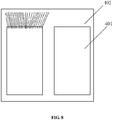
- the pads as illustrated in FIG. 7 are more than the pads as illustrated in FIG. 8 , thus a connecting line from the chip to the substrate is longer and an angle is larger, and more space is taken up.
- An objective of embodiments of the present disclosure is to provide a chip assembly and a chip to solve, at least to a certain extent, problems of more pads and fewer stacked layers in an existing chip assembly.
- a chip assembly includes a substrate, and a first chip and a second chip which are stacked on an upper surface of the substrate, wherein the first chip is arranged above the second chip. At edges of first sides of the first chip and the second chip, there are provided with first pad pairs, and a first pad pair includes a first reference potential pad and a second reference potential pad. At edges of second sides of the first chip and the second chip, there are provided with second pad pairs, and a second pad pair includes the first reference potential pad and the second reference potential pad.
- the second pad pair is arranged between two adjacent functional units at an outermost side of the edge of the second side of the first chip or the second chip, and a lower edge of the second pad pair is not lower than lower edges of the two adjacent functional units.
- a difference value between an orientation of the first side of the first chip and an orientation of the first side of the second chip is 180 degrees, and the first pad pair of the first chip corresponds in position to the second pad pair of the second chip.
- the first reference potential is a positive electrode of a power source
- the second reference potential is a ground potential
- the chip assembly further comprises a third chip and a fourth chip stacked, wherein the third chip and the fourth chip stacked being arranged side by side on the substrate together with the first chip and the second chip stacked.
- the upper surface of the edges, which correspond to the first side and the second side of the first chip, of the substrate is provided with connecting fingers.
- the pad pairs are arranged on the upper surfaces of the first chip and the second chip.
- the pad pairs which are on the first chip and the second chip, are coupled to the connecting fingers through bonding wires.
- the pad pair on the first side of the first chip is connected to the pad pair on the second side of the first chip through a power source cable.
- each of chip assemblies comprises a first chip and a second chip stacked and a third chip and a fourth chip stacked.
- the first chip comprises a peripheral logic control circuit and a memory cell array, and the peripheral logic control circuit being arranged on the first side of the first chip.
- other signal pad of the first chip except the first reference potential pad and the second reference potential pad are arranged at the edge of the first side of the first chip.
- the first reference potential pad of the first pad pair of the first chip corresponds in position to the first reference potential pad of the second pad pair of the second chip
- the second reference potential pad of the first pad pair of the first chip corresponds in position to the second reference potential pad of the second pad pair of the second chip
- a chip At an edge of a first side of the chip, there is provided with a first pad pair comprising a first reference potential pad and a second reference potential pad. At the edge of a second side of the chip, there is provided with a second pad pair comprising a first reference potential pad and the second reference potential pad.
- the second pad pair being arranged between two adjacent functional units at an outermost side of the edge of the second side of the chip, and a lower edge of the second pad pair is not lower than lower edges of the two adjacent functional units.
- the first reference potential pad of the first pad pair of the chip after the rotation corresponds in position to the first reference potential pad of the second pad pair of the chip before the rotation.
- the second reference potential pad of the first pad pair of the chip after the rotation corresponds in position to the second reference potential pad of the second pad pair of the chip before the rotation.
- the chip includes a dynamic random access memory chip, and the functional unit of the chip includes a memory cell array.
- pad pairs are respectively arranged on the first side and second side of the first chip and the first side and second side of the second chip, and the first pad pair of the first chip corresponds in position to the second pad pair of the second chip, which can reduce the number of pads of the chip and reduce the number of bonding points corresponding to the pad pairs on the substrate, such that the number of stackable layers can be increased in a fixed package space.
- the second pad pair is arranged between two adjacent functional units at an outermost side of the edge of the second side of the first chip or the second chip, which can further save the space for the chip. In this way, the pads can be arranged at the second side of the chip without taking up edge space of the second side.
- the embodiments of the present disclosure provide a chip assembly to reduce the number of pads of the chip to increase the number of stackable layers in a fixed package space.
- FIG. 9 schematically illustrates a schematic structural diagram of a chip according to an embodiment of the present disclosure.
- a first pad pair 901 including a first reference potential pad and a second reference potential pad.
- a second pad pair 902 including the first reference potential pad and the second reference potential pad.
- the second pad pair 902 is arranged between two adjacent functional units at an outermost side of the edge of the second side of the chip, and a lower edge of the second pad pair 902 is not lower than lower edges of the two adjacent functional units.
- the first reference potential pad of the first pad pair of the chip after the rotation corresponds in position to the first reference potential pad of the second pad pair of the chip before the rotation
- the second reference potential pad of the first pad pair of the chip after the rotation corresponds in position to the second reference potential pad of the second pad pair of the chip before the rotation
- the chip may be a dynamic random access memory chip, and the functional unit may be the memory cell array 104.
- the first reference potential may be a positive electrode of a power source
- the second reference potential may be a ground potential.
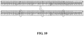
- an appropriate VSSQ (digital I/O port ground) and VQQ (digital ground) such as a pad 19, a pad 39 and a pad 60 are selected, and power source positive electrode (VDD2) pads such as a pad 18A, a pad 38A and a pad 60B are additionally provided beside these VSSQs and VQQs.
- VDD2 power source positive electrode
- the additionally provided power source positive electrode (VDD2) pads and the adjacent ground potential pads constitute a pad pair, i.e., a power source/ground pair to facilitate a remote pad distribution design.
- VDD2 power source positive electrode
- the VSSQ and the VSS actually are short-circuited.
- the VSSQ and the VSS are the same node.
- the exemplary embodiments of the present disclosure provide a chip assembly, which includes: a substrate, and a first chip and a second chip which are stacked on an upper surface of the substrate, wherein the first chip is arranged above the second chip.
- the first chip is the chip as illustrated in FIG. 9 .
- the first pad pair 901 including the first reference potential pad and the second reference potential pad.
- the second pad pair 902 including the first reference potential pad and the second reference potential pad.
- the second pad pair 902 is arranged between two adjacent functional units at an outermost side of the edge of the second side of the first chip, and the lower edge of the second pad pair 902 is not lower than the lower edges of the two adjacent functional units.
- the first pad pair including the first reference potential pad and the second reference potential pad.
- the second pad pair including the first reference potential pad and the second reference potential pad.
- the second pad pair is arranged between two adjacent functional units at the outermost side of the edge of the second side of the second chip, and the lower edge of the second pad pair is not lower than the lower edges of the two adjacent functional units.
- a difference value between an orientation of the first side of the first chip and an orientation of the first side of the second chip is 180 degrees, and the first pad pair of the first chip corresponds in position to the second pad pair of the second chip.
- pad pairs are provided at the edges of the first side and second side of the first chip and the edges of the first side and second side of the second chip, and the first pad pair of the first chip corresponds in position to the second pad pair of the second chip.
- one pad on the first side of the first chip and one pad on the second side of the second chip can correspond to the same connecting finger, such that the number of connecting fingers can be reduced.
- the second pad pair is positioned between the two adjacent functional units on the outermost side at the edge of the second side of the first chip or the second chip, which may save the space at the edge of the second side of the chip.
- a new power source/ground pad arrangement mode which can reduce equivalent resistance of a power source/ground cable and improve high-frequency performances of the chip without increasing the area.
- the first reference potential pad of the first pad pair of the first chip corresponds in position to the first reference potential pad of the second pad pair of the second chip; and the second reference potential pad of the first pad pair of the first chip corresponds in position to the second reference potential pad of the second pad pair of the second chip.
- three sets of pad pairs are arranged on the first side of the first chip.
- the left pad of the first pad pair from left to right is the power source positive electrode pad, and the right pad is a ground potential pad.
- the left pads of the second pad pair and the third pad pair from left to right are the ground potential pads, and the right pads are the power source positive electrode pads.
- Three sets of pad pairs are arranged on the second side of the first chip.
- the left pads of the first pad pair and the second pad pair from left to right are the power source positive electrode pads, and the right pads are the ground potential pads.
- the left pad of the third pad pair from left to right is the ground potential pad, and the right pad is the power source positive electrode pad.
- the second chip may have the same structure as the first chip.
- the three sets of power source/ground pads on the first side of the first chip above coincide in position with the power source/ground pads on the second side of the second chip below, and thus it is not required for additional area to place the pads, and also it is not required for providing additional connecting fingers on the substrate for connection in the process of packaging.
- some of logics such as decoding logics between the memory cell arrays 104 are up-and-down connection. Because there is no connecting line below the memory cell array at the bottom, some logics may be simplified or even deleted, and the power source/ground pads may be placed in vacant positions. Thus, the second pad pair may be arranged between two adjacent functional units at an outermost side of the edge of the second side of the first chip or second chip to reduce the area of the chip.
- the pad pair arranged on the first side of the first chip is connected to the pad pair arranged on the second side of the first chip through a power source cable 903.
- the first chip includes a peripheral logic control circuit 103 and the memory cell array 104, and the peripheral logic control circuit 103 is arranged on the first side of the first chip.
- Another signal pad of the first chip except the first reference potential pad and the second reference potential pad is arranged at the edge of the first side of the first chip.
- the aother signal pad includes a data input/output port pad, a command address port pad, and a clock port pad.
- the chip assembly further includes a third chip and a fourth chip stacked.
- a stacked assembly formed by the first chip and the second chip and a stacked assembly formed by the third chip and the fourth chip are arranged side by side on the substrate.
- the number of chips in the stacked assembly formed by the first chip and the second chip on the substrate is two.
- the number of chips in the stacked assembly formed by the first chip and the second chip is not limited thereto.
- the number of chips in the stacked assembly formed by the third chip and the fourth chip may be two or more.
- each chip assembly includes the first chip and the second chip stacked and the third chip and the fourth chip stacked.
- the first chip 1101 and the second chip 1102 are stacked on a substrate 402.
- a power source positive electrode pad 1105 and a ground potential pad 1106 are respectively coupled to a connecting finger 1103 and a connecting finger 1104 through a bonding wire 1107.
- the connecting fingers are arranged on the upper surface of the substrate, and the pad pairs may also be arranged on the upper surfaces of the edges of the first side and second side of the first chip and the upper surfaces of the edges of the first side and second side of the second chip.
- the pad pairs may also be arranged on the upper surfaces of the third chip and the fourth chip.
- the pad pairs on the third chip and the fourth chip may also be coupled to the connecting fingers through the bonding wires.
- the pad pair may include the power source positive electrode pad 1105 and the ground potential pad 1106.
- pad pairs are respectively arranged on the first side and second side of the first chip and the first side and second side of the second chip, and the first pad pair of the first chip corresponds in position to the second pad pair of the second chip, which can reduce the number of pads of the chip and reduce the number of bonding points corresponding to the pad pairs on the substrate, such that the number of stackable layers can be increased in a fixed package space.
- the second pad pair is arranged between two adjacent functional units at an outermost side of the edge of the second side of the first chip or the second chip, which can further save the space for the chip. In this way, the pads can be arranged at the second side of the chip without taking up edge space of the second side.
Landscapes
- Engineering & Computer Science (AREA)
- Microelectronics & Electronic Packaging (AREA)
- Semiconductor Integrated Circuits (AREA)
- Semiconductor Memories (AREA)
Abstract
Description
- The present disclosure claims priority to
Chinese Patent Application No. 201911176109.X, titled "CHIP COMBINATION AND CHIP" and filed on November 26, 2019 - The present disclosure relates to the field of semiconductor technologies, and more particularly, to a chip assembly and a chip.
- At present, a low-power consumption dynamic random-access memory (DRAM) generally has nearly a hundred or more pads, including data input/output ports, command address ports, clock ports, and multiple sets of power source/ground ports. As a constituent part of distributed power supply, the multiple sets of power source/ground ports can increase power supply balance and consistency of the power source/ground. Pad layouts of a chip generally have the following types.
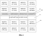
- As illustrated in
FIG 1 , by placing the pads and a peripherallogic control circuit 103 in the middle portion of the chip, i.e., betweenmemory cell arrays 104, a distance from power source/ground pads to two edges of the chip is only half of a height of the chip, a parasitic resistance will be reduced by half, and a voltage drop on a power source/ground cable will be reduced by half under the conditions of the same width of the power source/ground cable and the same current. In this way, noise can be reduced, and drive capability can be increased, which is particularly advantageous to a high-frequency operating mode of the chip. However, this method is not advantageous to large-capacity stacked package. To implement the stacked package, it is required to introduce a re-distribution layer (RDL) to lead the middle pads to a side of the chip, which increases the complexity of processes and increases fabrication costs. Furthermore, the parasitic resistance generated by the introduced RDL may also weaken the advantages of low resistance obtained by placing the pads in the middle of the chip. - As illustrated in
FIG. 2 , the pads and the peripheral control logic circuit are arranged on a certain side of the chip, especially on a shorter side. In this case, the power source/ground cable is the longest, the parasitic resistance is the largest, and the voltage drop is the largest at a far end of the chip away from the pads, which may cause the performance of the chip at the far end to be much worse than the performance of the chip at a near end, especially in the high-frequency operating mode. To ensure the chip to operate properly at the far end, the required power source/ground cable has to be widened, which takes up the space of other signal lines and increases difficulties in layout design. - As illustrated in
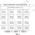
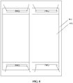
FIG. 3 , the peripheral control logic circuit and a part of the pads are arranged on one side of the chip, and another part of the pads are arranged on the other side of the chip. The pads include distributed power source/ground pads 102 andother signal pads 101. In this way, the equivalent resistance and the cable area of the power source/ground cable can also be reduced. However, the increase of the area of a row of pads directly increases the fabrication costs of the chip. Furthermore, the layout of the pads on two sides may have adverse effects on the large-capacity and miniaturized package of the chip. - At present, the package of the low-power consumption DRAM tends to large capacity and miniaturization. That is, it is expected that a large number of low-power consumption DRAM particles can be packaged in one package cavity to increase the capacity and reduce the power consumption. This requires that the DRAM chips can support a stacked package. Under the premise of not considering the expensive Through Silicon Via (TSV) technology, in the stacked package as illustrated in
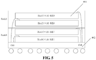
FIG. 4 andFIG. 5 , achip 401 is arranged on asubstrate 402, and the stacked package cannot be achieved conveniently unless the pads are arranged at the edge of the chip. - The more the stacked layers of the chip are, the longer a bonding wire from the chip to the substrate is, and the larger the space occupied is. Under the condition of limited package internal cavity space, the size of the chip, the number of pads connected on the substrate and the number of stacked layers are mutually restrictive. That is, the smaller the size of the chip is and the fewer the number of pads is, the more layers can be stacked. The chip as illustrated in
FIG. 5 is smaller in size than the chip as illustrated inFIG. 6 , and thus more layers can be stacked. The pads as illustrated inFIG. 7 are more than the pads as illustrated inFIG. 8 , thus a connecting line from the chip to the substrate is longer and an angle is larger, and more space is taken up. - There are more pads and fewer stacked layers in a chip assembly, which is a technical problem to be solved urgently at present.
- It is to be noted that the above information disclosed in this Background portion is only for the purpose of enhancing understanding of the background of the present disclosure, and thus it may include information which does not constitute the prior art known to those of ordinary skill in the art.
- An objective of embodiments of the present disclosure is to provide a chip assembly and a chip to solve, at least to a certain extent, problems of more pads and fewer stacked layers in an existing chip assembly.
- Other features and advantages of the present disclosure will become apparent from the following detailed description, or will be obtained in part, by practice of the present disclosure.
- According to a first aspect of the embodiments of the present disclosure, there is provided a chip assembly. The chip assembly includes a substrate, and a first chip and a second chip which are stacked on an upper surface of the substrate, wherein the first chip is arranged above the second chip. At edges of first sides of the first chip and the second chip, there are provided with first pad pairs, and a first pad pair includes a first reference potential pad and a second reference potential pad. At edges of second sides of the first chip and the second chip, there are provided with second pad pairs, and a second pad pair includes the first reference potential pad and the second reference potential pad. The second pad pair is arranged between two adjacent functional units at an outermost side of the edge of the second side of the first chip or the second chip, and a lower edge of the second pad pair is not lower than lower edges of the two adjacent functional units. A difference value between an orientation of the first side of the first chip and an orientation of the first side of the second chip is 180 degrees, and the first pad pair of the first chip corresponds in position to the second pad pair of the second chip.
- In some embodiments, the first reference potential is a positive electrode of a power source, and the second reference potential is a ground potential.
- In some embodiments, the chip assembly further comprises a third chip and a fourth chip stacked, wherein the third chip and the fourth chip stacked being arranged side by side on the substrate together with the first chip and the second chip stacked.
- In some embodiments, the upper surface of the edges, which correspond to the first side and the second side of the first chip, of the substrate is provided with connecting fingers.
- In some embodiments, the pad pairs are arranged on the upper surfaces of the first chip and the second chip.
- In some embodiments, the pad pairs, which are on the first chip and the second chip, are coupled to the connecting fingers through bonding wires.
- In some embodiments, the pad pair on the first side of the first chip is connected to the pad pair on the second side of the first chip through a power source cable.
- In some embodiments, each of chip assemblies comprises a first chip and a second chip stacked and a third chip and a fourth chip stacked.
- In some embodiments, the first chip comprises a peripheral logic control circuit and a memory cell array, and the peripheral logic control circuit being arranged on the first side of the first chip.
- In some embodiments, other signal pad of the first chip except the first reference potential pad and the second reference potential pad are arranged at the edge of the first side of the first chip.
- In some embodiments, the first reference potential pad of the first pad pair of the first chip corresponds in position to the first reference potential pad of the second pad pair of the second chip, and the second reference potential pad of the first pad pair of the first chip corresponds in position to the second reference potential pad of the second pad pair of the second chip.
- According to a second aspect of the embodiments of the present disclosure, there is provided a chip. At an edge of a first side of the chip, there is provided with a first pad pair comprising a first reference potential pad and a second reference potential pad. At the edge of a second side of the chip, there is provided with a second pad pair comprising a first reference potential pad and the second reference potential pad. The second pad pair being arranged between two adjacent functional units at an outermost side of the edge of the second side of the chip, and a lower edge of the second pad pair is not lower than lower edges of the two adjacent functional units. After the chip is rotated by 180 degrees in a plane where the chip is located, the first pad pair on the first side of the chip after the rotation corresponds in position to the second pad pair on the second side of the chip before the rotation.
- In some embodiments, the first reference potential pad of the first pad pair of the chip after the rotation corresponds in position to the first reference potential pad of the second pad pair of the chip before the rotation. The second reference potential pad of the first pad pair of the chip after the rotation corresponds in position to the second reference potential pad of the second pad pair of the chip before the rotation.
- In some embodiments, the chip includes a dynamic random access memory chip, and the functional unit of the chip includes a memory cell array.
- The technical solutions provided by the embodiments of the present disclosure may include following beneficial effects.
- In the technical solutions provided by some embodiments of the present disclosure, pad pairs are respectively arranged on the first side and second side of the first chip and the first side and second side of the second chip, and the first pad pair of the first chip corresponds in position to the second pad pair of the second chip, which can reduce the number of pads of the chip and reduce the number of bonding points corresponding to the pad pairs on the substrate, such that the number of stackable layers can be increased in a fixed package space. In addition, the second pad pair is arranged between two adjacent functional units at an outermost side of the edge of the second side of the first chip or the second chip, which can further save the space for the chip. In this way, the pads can be arranged at the second side of the chip without taking up edge space of the second side. It is to be understood that the above general description and the detailed description below are merely exemplary and explanatory, and do not limit the present disclosure.
- The accompanying drawings, which are incorporated in and constitute a part of this specification, illustrate embodiments consistent with the disclosure and, together with the description, serve to explain the principles of the disclosure. It is apparent that the drawings in the following description are merely some embodiments of the present disclosure. For those skilled in the art, other drawings can be obtained according to these drawings without creative efforts.
-
FIG. 1 schematically illustrates a schematic diagram of a chip layout in the related technologies; -
FIG. 2 schematically illustrates a schematic diagram of another chip layout in the related technologies; -
FIG. 3 schematically illustrates a schematic diagram of still another chip layout in the related technologies; -
FIG. 4 schematically illustrates a vertical view of still another chip layout in the related technologies; -
FIG. 5 schematically illustrates a sectional view of still another chip layout in the related technologies; -
FIG. 6 schematically illustrates a sectional view of still another chip layout in the related technologies; -
FIG. 7 schematically illustrates a schematic diagram of connection between a chip and a substrate in the related technologies; -
FIG. 8 schematically illustrates a schematic diagram of connection between another chip and a substrate in the related technologies; -
FIG. 9 schematically illustrates a schematic structural diagram of a chip according to an embodiment of the present disclosure; -
FIG. 10 schematically illustrates a schematic diagram showing variation of pad pins according to an embodiment of the present disclosure; and -
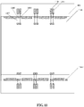
FIG. 11 schematically illustrates a schematic structural diagram of a chip assembly according to an embodiment of the present disclosure. - In the drawings: another
signal pad 101; power source/ground pad 102; peripherallogic control circuit 103;memory cell array 104;chip 401;substrate 402;first pad pair 901;second pad pair 902;power source cable 903;first chip 1101;second chip 1102; connectingfinger 1103; connectingfinger 1104; power sourcepositive electrode pad 1105;ground potential pad 1106;bonding wire 1107. - Exemplary embodiments will be described more comprehensively by referring to the accompanying drawings now. However, the exemplary embodiments may be carried out in various manners, and shall not be interpreted as being limited to the embodiments set forth herein; instead, providing these embodiments will make the present disclosure more comprehensive and complete, and will fully convey the conception of the exemplary embodiments to those skilled in the art. Throughout the drawings, similar reference signs indicate the same or similar structures, and their detailed description will be omitted.
- In the related technologies, in the same package internal cavity space, the more pads of a chip of a chip assembly are, the fewer stackable layers of the chip are, which in turn affects functions of the chip assembly.
- To solve the above-mentioned problem, the embodiments of the present disclosure provide a chip assembly to reduce the number of pads of the chip to increase the number of stackable layers in a fixed package space.
-
FIG. 9 schematically illustrates a schematic structural diagram of a chip according to an embodiment of the present disclosure. - As illustrated in
FIG. 9 , in the chip provided by the embodiments of the present disclosure, at an edge of a first side of the chip, there is provided with afirst pad pair 901 including a first reference potential pad and a second reference potential pad. At the edge of a second side of the chip, there is provided with asecond pad pair 902 including the first reference potential pad and the second reference potential pad. Thesecond pad pair 902 is arranged between two adjacent functional units at an outermost side of the edge of the second side of the chip, and a lower edge of thesecond pad pair 902 is not lower than lower edges of the two adjacent functional units. After the chip is rotated by 180 degrees in a plane where the chip is located, the pad pair on the first side of the chip after the rotation corresponds in position to the pad pair on the second side of the chip before the rotation. - In this way, the first reference potential pad of the first pad pair of the chip after the rotation corresponds in position to the first reference potential pad of the second pad pair of the chip before the rotation, and the second reference potential pad of the first pad pair of the chip after the rotation corresponds in position to the second reference potential pad of the second pad pair of the chip before the rotation.
- Here, the chip may be a dynamic random access memory chip, and the functional unit may be the
memory cell array 104. The first reference potential may be a positive electrode of a power source, and the second reference potential may be a ground potential. As illustrated inFIG. 10 , according to a pad order recommended by Joint Electron Device Engineering Council Solid State Technology Association (JEDEC) and according to an arrangement position of thememory cell array 104, an appropriate VSSQ (digital I/O port ground) and VQQ (digital ground) such as a pad 19, a pad 39 and a pad 60 are selected, and power source positive electrode (VDD2) pads such as a pad 18A, a pad 38A and a pad 60B are additionally provided beside these VSSQs and VQQs. The additionally provided power source positive electrode (VDD2) pads and the adjacent ground potential pads constitute a pad pair, i.e., a power source/ground pair to facilitate a remote pad distribution design. Here, the VSSQ and the VSS actually are short-circuited. In other words, the VSSQ and the VSS are the same node. - The exemplary embodiments of the present disclosure provide a chip assembly, which includes: a substrate, and a first chip and a second chip which are stacked on an upper surface of the substrate, wherein the first chip is arranged above the second chip. Here, the first chip is the chip as illustrated in
FIG. 9 . - As illustrated in
FIG. 9 , at the edge of the first side of the chip, there is provided with thefirst pad pair 901 including the first reference potential pad and the second reference potential pad. At the edge of the second side of the first chip, there is provided with thesecond pad pair 902 including the first reference potential pad and the second reference potential pad. Thesecond pad pair 902 is arranged between two adjacent functional units at an outermost side of the edge of the second side of the first chip, and the lower edge of thesecond pad pair 902 is not lower than the lower edges of the two adjacent functional units. At the edge of the first side of the second chip, there is provided with the first pad pair including the first reference potential pad and the second reference potential pad. At the edge of the second side of the second chip, there is provided with the second pad pair including the first reference potential pad and the second reference potential pad. The second pad pair is arranged between two adjacent functional units at the outermost side of the edge of the second side of the second chip, and the lower edge of the second pad pair is not lower than the lower edges of the two adjacent functional units. A difference value between an orientation of the first side of the first chip and an orientation of the first side of the second chip is 180 degrees, and the first pad pair of the first chip corresponds in position to the second pad pair of the second chip. - According to the technical solutions provided by the embodiments of the present disclosure, pad pairs are provided at the edges of the first side and second side of the first chip and the edges of the first side and second side of the second chip, and the first pad pair of the first chip corresponds in position to the second pad pair of the second chip. In this way, when the pad pairs are bonded to connecting fingers on the substrate, one pad on the first side of the first chip and one pad on the second side of the second chip can correspond to the same connecting finger, such that the number of connecting fingers can be reduced.
- In addition, the second pad pair is positioned between the two adjacent functional units on the outermost side at the edge of the second side of the first chip or the second chip, which may save the space at the edge of the second side of the chip. In comprehensive consideration of various factors such as package feasibility, power source/ground pad layout, wiring resources and utilization ratio, distribution of modules in the chip, chip area and fabrication costs, what is provided by the present disclosure is a new power source/ground pad arrangement mode, which can reduce equivalent resistance of a power source/ground cable and improve high-frequency performances of the chip without increasing the area.
- In the embodiments of the present disclosure, the first reference potential pad of the first pad pair of the first chip corresponds in position to the first reference potential pad of the second pad pair of the second chip; and the second reference potential pad of the first pad pair of the first chip corresponds in position to the second reference potential pad of the second pad pair of the second chip.
- As illustrated in
FIG. 9 , three sets of pad pairs are arranged on the first side of the first chip. The left pad of the first pad pair from left to right is the power source positive electrode pad, and the right pad is a ground potential pad. The left pads of the second pad pair and the third pad pair from left to right are the ground potential pads, and the right pads are the power source positive electrode pads. Three sets of pad pairs are arranged on the second side of the first chip. The left pads of the first pad pair and the second pad pair from left to right are the power source positive electrode pads, and the right pads are the ground potential pads. The left pad of the third pad pair from left to right is the ground potential pad, and the right pad is the power source positive electrode pad. The second chip may have the same structure as the first chip. - In this way, when the first pad pair of the first chip corresponds in position to the second pad pair of the second chip, the three sets of power source/ground pads on the first side of the first chip above coincide in position with the power source/ground pads on the second side of the second chip below, and thus it is not required for additional area to place the pads, and also it is not required for providing additional connecting fingers on the substrate for connection in the process of packaging.
- In addition, some of logics such as decoding logics between the
memory cell arrays 104 are up-and-down connection. Because there is no connecting line below the memory cell array at the bottom, some logics may be simplified or even deleted, and the power source/ground pads may be placed in vacant positions. Thus, the second pad pair may be arranged between two adjacent functional units at an outermost side of the edge of the second side of the first chip or second chip to reduce the area of the chip. - As illustrated in
FIG. 9 , the pad pair arranged on the first side of the first chip is connected to the pad pair arranged on the second side of the first chip through apower source cable 903. The first chip includes a peripherallogic control circuit 103 and thememory cell array 104, and the peripherallogic control circuit 103 is arranged on the first side of the first chip. Another signal pad of the first chip except the first reference potential pad and the second reference potential pad is arranged at the edge of the first side of the first chip. Here, the aother signal pad includes a data input/output port pad, a command address port pad, and a clock port pad. - In the embodiments of the present disclosure, the chip assembly further includes a third chip and a fourth chip stacked. A stacked assembly formed by the first chip and the second chip and a stacked assembly formed by the third chip and the fourth chip are arranged side by side on the substrate.
- As illustrated in
FIG. 11 , the number of chips in the stacked assembly formed by the first chip and the second chip on the substrate is two. However, in practical applications, the number of chips in the stacked assembly formed by the first chip and the second chip is not limited thereto. Similarly, the number of chips in the stacked assembly formed by the third chip and the fourth chip may be two or more. For example, in one embodiment, each chip assembly includes the first chip and the second chip stacked and the third chip and the fourth chip stacked. - As illustrated in
FIG. 11 , thefirst chip 1101 and thesecond chip 1102 are stacked on asubstrate 402. A power sourcepositive electrode pad 1105 and aground potential pad 1106 are respectively coupled to a connectingfinger 1103 and a connectingfinger 1104 through abonding wire 1107. In the embodiments of the present disclosure, on the upper surface of the edges, which correspond to the first side and the second side of the first chip, of the substrate, there is provided with connecting fingers. The connecting fingers are arranged on the upper surface of the substrate, and the pad pairs may also be arranged on the upper surfaces of the edges of the first side and second side of the first chip and the upper surfaces of the edges of the first side and second side of the second chip. - Similarly, the pad pairs may also be arranged on the upper surfaces of the third chip and the fourth chip. The pad pairs on the third chip and the fourth chip may also be coupled to the connecting fingers through the bonding wires. Here, the pad pair may include the power source
positive electrode pad 1105 and theground potential pad 1106. - In the chip assembly provided by the embodiments of the present disclosure, pad pairs are respectively arranged on the first side and second side of the first chip and the first side and second side of the second chip, and the first pad pair of the first chip corresponds in position to the second pad pair of the second chip, which can reduce the number of pads of the chip and reduce the number of bonding points corresponding to the pad pairs on the substrate, such that the number of stackable layers can be increased in a fixed package space. In addition, the second pad pair is arranged between two adjacent functional units at an outermost side of the edge of the second side of the first chip or the second chip, which can further save the space for the chip. In this way, the pads can be arranged at the second side of the chip without taking up edge space of the second side.
- Although this specification uses relativity terms such as "above" and "below" to describe a relative relation between one component and another component of icons, these terms are merely for convenience of this specification, for example, the directions of the examples in the accompanying drawings. It is to be understood that when the apparatus of the icon are turned upside down, components described as "above" will become components described as "below". When a certain structure is "above" other structures, it likely means that a certain structure is integrally formed on other structures, or a certain structure is "directly" arranged on other structures, or a certain structure is "indirectly" arranged on other structures by means of another structure.
- The terms "one", "a", "the", "said", and "at least one" are intended to mean that there exists one or more elements/constituent parts/etc. The terms "comprising" and "having" are intended to be inclusive and mean that there may be additional elements/constituent parts/etc. other than the listed elements/constituent parts/etc.
- Other embodiments of the present disclosure will be apparent to those skilled in the art from consideration of the specification and practice of the invention disclosed here. The present disclosure is intended to cover any variations, uses, or adaptations of the present disclosure following the general principles thereof and including such departures from the present disclosure as come within known or customary practice in the art. It is intended that the specification and embodiments be considered as exemplary only, with a true scope and spirit of the present disclosure being indicated by the appended claims.
Claims (14)
- A chip assembly, comprising: a substrate, a first chip and a second chip which are stacked on an upper surface of the substrate, wherein the first chip is arranged above the second chip; wherein
first pad pairs are provided at edges of first sides of the first chip and the second chip, a first pad pair comprises a first reference potential pad and a second reference potential pad; and second pad pairs are provided at edges of second sides of the first chip and the second chip, and a second pad pair comprises a first reference potential pad and a second reference potential pad; the second pad pair is arranged between two adjacent functional units at an outermost side of the edge of the second side of the first chip or the second chip, and a lower edge of the second pad pair is not lower than lower edges of the two adjacent functional units; and
a difference value between an orientation of the first side of the first chip and an orientation of the first side of the second chip is 180 degrees, and the first pad pair of the first chip corresponds in position to the second pad pair of the second chip. - The chip assembly according to claim 1, wherein a first reference potential is a positive electrode of a power source, and a second reference potential is a ground potential.
- The chip assembly according to claim 1, wherein the chip assembly further comprises a third chip and a fourth chip stacked, the third chip and the fourth chip stacked being arranged side by side on the substrate together with the first chip and the second chip stacked.
- The chip assembly according to claim 3, wherein the upper surface of the edges, which correspond to the first side and the second side of the first chip, of the substrate is provided with connecting fingers.
- The chip assembly according to claim 4, wherein the pad pairs are arranged on the upper surfaces of the first chip and the second chip.
- The chip assembly according to claim 4, wherein the pad pairs, which are on the first chip and the second chip, are coupled to the connecting fingers through bonding wires.
- The chip assembly according to claim 1, wherein the pad pair on the first side of the first chip is connected to the pad pair on the second side of the first chip through a power source cable.
- The chip assembly according to claim 1, wherein each of chip assemblies comprises a first chip and a second chip stacked, and a third chip and a fourth chip stacked.
- The chip assembly according to claim 1, wherein the first chip comprises a peripheral logic control circuit and a memory cell array, the peripheral logic control circuit being arranged on the first side of the first chip.
- The chip assembly according to claim 1, wherein other signal pads of the first chip except the first reference potential pad and the second reference potential pad are arranged at the edge of the first side of the first chip.
- The chip assembly according to claim 1, wherein the first reference potential pad of the first pad pair of the first chip corresponds in position to the first reference potential pad of the second pad pair of the second chip, and the second reference potential pad of the first pad pair of the first chip corresponds in position to the second reference potential pad of the second pad pair of the second chip.
- A chip, wherein at an edge of a first side of the chip, there is provided with a first pad pair comprising a first reference potential pad and a second reference potential pad, at an edge of a second side of the chip, there is provided with a second pad pair comprising a first reference potential pad and a second reference potential pad, the second pad pair being arranged between two adjacent functional units at an outermost side of the edge of the second side of the chip, and a lower edge of the second pad pair being not lower than lower edges of the two adjacent functional units;
wherein after the chip is rotated by 180 degrees in a plane where the chip is located, the first pad pair on the first side of the chip after the rotation corresponds in position to the second pad pair on the second side of the chip before the rotation. - The chip according to claim 12, wherein the first reference potential pad of the first pad pair of the chip after the rotation corresponds in position to the first reference potential pad of the second pad pair of the chip before the rotation, and the second reference potential pad of the first pad pair of the chip after the rotation corresponds in position to the second reference potential pad of the second pad pair of the chip before the rotation.
- The chip according to claim 12, wherein the chip comprises a dynamic random access memory chip, and the functional unit of the chip comprises a memory cell array.
Applications Claiming Priority (2)
| Application Number | Priority Date | Filing Date | Title |
|---|---|---|---|
| CN201911176109.XA CN112951811B (en) | 2019-11-26 | 2019-11-26 | Chipset and Chip |
| PCT/CN2020/107430 WO2021103642A1 (en) | 2019-11-26 | 2020-08-06 | Chip combination and chip |
Publications (3)
| Publication Number | Publication Date |
|---|---|
| EP3923325A1 true EP3923325A1 (en) | 2021-12-15 |
| EP3923325A4 EP3923325A4 (en) | 2022-06-15 |
| EP3923325B1 EP3923325B1 (en) | 2024-06-19 |
Family
ID=76129949
Family Applications (1)
| Application Number | Title | Priority Date | Filing Date |
|---|---|---|---|
| EP20892133.8A Active EP3923325B1 (en) | 2019-11-26 | 2020-08-06 | Chip combination and chip |
Country Status (4)
| Country | Link |
|---|---|
| US (1) | US11164849B2 (en) |
| EP (1) | EP3923325B1 (en) |
| CN (1) | CN112951811B (en) |
| WO (1) | WO2021103642A1 (en) |
Family Cites Families (12)
| Publication number | Priority date | Publication date | Assignee | Title |
|---|---|---|---|---|
| JP2792795B2 (en) * | 1992-10-29 | 1998-09-03 | 三菱電機株式会社 | Semiconductor integrated device |
| KR100384056B1 (en) * | 1999-06-03 | 2003-05-14 | 삼성전자주식회사 | Semiconductor memory device and data output buffer thereof |
| US6870273B2 (en) * | 2002-04-29 | 2005-03-22 | Pmc-Sierra, Inc. | High speed I/O pad and pad/cell interconnection for flip chips |
| JP2006140466A (en) * | 2005-10-21 | 2006-06-01 | Renesas Technology Corp | Semiconductor memory device |
| JP4921937B2 (en) * | 2006-11-24 | 2012-04-25 | 株式会社東芝 | Semiconductor integrated circuit |
| CN102437147B (en) * | 2011-12-09 | 2014-04-30 | 天水华天科技股份有限公司 | Dense-pitch small-pad copper-line bonded intelligent card (IC) chip stacking packing piece and preparation method thereof |
| KR102211934B1 (en) * | 2014-03-06 | 2021-02-04 | 삼성전자주식회사 | Semiconductor package |
| KR102398663B1 (en) * | 2015-07-09 | 2022-05-16 | 삼성전자주식회사 | semiconductor chip including chip pad, redistribution wiring test pad and redistribution wiring connection pad |
| CN206532776U (en) * | 2017-02-17 | 2017-09-29 | 成都芯锐科技有限公司 | Multichip stacking encapsulation structure |
| CN108010898A (en) * | 2017-11-02 | 2018-05-08 | 上海玮舟微电子科技有限公司 | A kind of chip-packaging structure |
| CN108962881A (en) * | 2018-07-03 | 2018-12-07 | 华进半导体封装先导技术研发中心有限公司 | Stack package structure |
| CN210640244U (en) * | 2019-11-26 | 2020-05-29 | 长鑫存储技术有限公司 | Chip combination and chip |
-
2019
- 2019-11-26 CN CN201911176109.XA patent/CN112951811B/en active Active
-
2020
- 2020-08-06 WO PCT/CN2020/107430 patent/WO2021103642A1/en not_active Ceased
- 2020-08-06 EP EP20892133.8A patent/EP3923325B1/en active Active
-
2021
- 2021-03-09 US US17/196,926 patent/US11164849B2/en active Active
Also Published As
| Publication number | Publication date |
|---|---|
| CN112951811B (en) | 2025-09-05 |
| US11164849B2 (en) | 2021-11-02 |
| CN112951811A (en) | 2021-06-11 |
| EP3923325A4 (en) | 2022-06-15 |
| US20210265316A1 (en) | 2021-08-26 |
| EP3923325B1 (en) | 2024-06-19 |
| WO2021103642A1 (en) | 2021-06-03 |
Similar Documents
| Publication | Publication Date | Title |
|---|---|---|
| US7834450B2 (en) | Semiconductor package having memory devices stacked on logic device | |
| KR102716191B1 (en) | Semiconductor memory device and memory module having the same | |
| TWI691037B (en) | Face-to-face mounting integrated circuit die with orthogonal top interconnect layer | |
| JP4753725B2 (en) | Multilayer semiconductor device | |
| US7663903B2 (en) | Semiconductor memory device having improved voltage transmission path and driving method thereof | |
| US20200098724A1 (en) | Semiconductor package or structure with dual-sided interposers and memory | |
| US20100052111A1 (en) | Stacked-chip device | |
| US20200402959A1 (en) | Stacked semiconductor package having an interposer | |
| US20150155266A1 (en) | Semiconductor package | |
| TWI761632B (en) | Semiconductor packages including bridge die spaced apart from semiconductor die | |
| US9466593B2 (en) | Stack semiconductor package | |
| KR20130078458A (en) | Semiconductor package with pop(package on package) structure | |
| US7745932B2 (en) | Semiconductor package, semiconductor package module including the semiconductor package, and methods of fabricating the same | |
| US11164849B2 (en) | Chip assembly and chip | |
| CN210640244U (en) | Chip combination and chip | |
| JP4754201B2 (en) | Semiconductor device | |
| CN111508921A (en) | Semiconductor chip set with double-sided external contact | |
| CN215955274U (en) | Three-dimensional heterogeneous integrated programmable chip structure and electronic equipment | |
| US20050104206A1 (en) | Mounting structure in integrated circuit module | |
| US20090039529A1 (en) | Integrated Circuit Having a Plurality of Connection Pads and Integrated Circuit Package | |
| CN103875072A (en) | Integrated circuit, multi-core processor device and method for manufacturing integrated circuit | |
| CN101599480B (en) | Semiconductor chip encapsulating structure | |
| KR102917154B1 (en) | Stacked semiconductor device | |
| US20260101828A1 (en) | Semiconductor module | |
| US20250112194A1 (en) | 3d chip package structure |
Legal Events
| Date | Code | Title | Description |
|---|---|---|---|
| STAA | Information on the status of an ep patent application or granted ep patent |
Free format text: STATUS: THE INTERNATIONAL PUBLICATION HAS BEEN MADE |
|
| PUAI | Public reference made under article 153(3) epc to a published international application that has entered the european phase |
Free format text: ORIGINAL CODE: 0009012 |
|
| STAA | Information on the status of an ep patent application or granted ep patent |
Free format text: STATUS: REQUEST FOR EXAMINATION WAS MADE |
|
| 17P | Request for examination filed |
Effective date: 20210907 |
|
| AK | Designated contracting states |
Kind code of ref document: A1 Designated state(s): AL AT BE BG CH CY CZ DE DK EE ES FI FR GB GR HR HU IE IS IT LI LT LU LV MC MK MT NL NO PL PT RO RS SE SI SK SM TR |
|
| REG | Reference to a national code |
Ref country code: DE Ref legal event code: R079 Free format text: PREVIOUS MAIN CLASS: H01L0025070000 Ipc: H01L0025065000 Ref country code: DE Ref legal event code: R079 Ref document number: 602020032793 Country of ref document: DE Free format text: PREVIOUS MAIN CLASS: H01L0025070000 Ipc: H01L0025065000 |
|
| A4 | Supplementary search report drawn up and despatched |
Effective date: 20220513 |
|
| RIC1 | Information provided on ipc code assigned before grant |
Ipc: G11C 5/06 20060101ALI20220509BHEP Ipc: G11C 5/02 20060101ALI20220509BHEP Ipc: H01L 23/485 20060101ALI20220509BHEP Ipc: H01L 23/50 20060101ALI20220509BHEP Ipc: H01L 25/065 20060101AFI20220509BHEP |
|
| STAA | Information on the status of an ep patent application or granted ep patent |
Free format text: STATUS: EXAMINATION IS IN PROGRESS |
|
| DAV | Request for validation of the european patent (deleted) | ||
| DAX | Request for extension of the european patent (deleted) | ||
| 17Q | First examination report despatched |
Effective date: 20230223 |
|
| REG | Reference to a national code |
Ref country code: DE Ref legal event code: R079 Ipc: G11C0005020000 Ref country code: DE Ref legal event code: R079 Ref document number: 602020032793 Country of ref document: DE Free format text: PREVIOUS MAIN CLASS: H01L0025065000 Ipc: G11C0005020000 |
|
| GRAP | Despatch of communication of intention to grant a patent |
Free format text: ORIGINAL CODE: EPIDOSNIGR1 |
|
| STAA | Information on the status of an ep patent application or granted ep patent |
Free format text: STATUS: GRANT OF PATENT IS INTENDED |
|
| RIC1 | Information provided on ipc code assigned before grant |
Ipc: G11C 5/06 20060101ALN20240229BHEP Ipc: H01L 25/065 20060101ALI20240229BHEP Ipc: H01L 23/49 20060101ALI20240229BHEP Ipc: H01L 23/485 20060101ALI20240229BHEP Ipc: G11C 5/02 20060101AFI20240229BHEP |
|
| INTG | Intention to grant announced |
Effective date: 20240322 |
|
| RAP3 | Party data changed (applicant data changed or rights of an application transferred) |
Owner name: CHANGXIN MEMORY TECHNOLOGIES, INC. |
|
| GRAS | Grant fee paid |
Free format text: ORIGINAL CODE: EPIDOSNIGR3 |
|
| GRAA | (expected) grant |
Free format text: ORIGINAL CODE: 0009210 |
|
| STAA | Information on the status of an ep patent application or granted ep patent |
Free format text: STATUS: THE PATENT HAS BEEN GRANTED |
|
| AK | Designated contracting states |
Kind code of ref document: B1 Designated state(s): AL AT BE BG CH CY CZ DE DK EE ES FI FR GB GR HR HU IE IS IT LI LT LU LV MC MK MT NL NO PL PT RO RS SE SI SK SM TR |
|
| REG | Reference to a national code |
Ref country code: GB Ref legal event code: FG4D |
|
| REG | Reference to a national code |
Ref country code: CH Ref legal event code: EP |
|
| P01 | Opt-out of the competence of the unified patent court (upc) registered |
Effective date: 20240528 |
|
| REG | Reference to a national code |
Ref country code: DE Ref legal event code: R096 Ref document number: 602020032793 Country of ref document: DE |
|
| PG25 | Lapsed in a contracting state [announced via postgrant information from national office to epo] |
Ref country code: BG Free format text: LAPSE BECAUSE OF FAILURE TO SUBMIT A TRANSLATION OF THE DESCRIPTION OR TO PAY THE FEE WITHIN THE PRESCRIBED TIME-LIMIT Effective date: 20240619 |
|
| PG25 | Lapsed in a contracting state [announced via postgrant information from national office to epo] |
Ref country code: HR Free format text: LAPSE BECAUSE OF FAILURE TO SUBMIT A TRANSLATION OF THE DESCRIPTION OR TO PAY THE FEE WITHIN THE PRESCRIBED TIME-LIMIT Effective date: 20240619 Ref country code: FI Free format text: LAPSE BECAUSE OF FAILURE TO SUBMIT A TRANSLATION OF THE DESCRIPTION OR TO PAY THE FEE WITHIN THE PRESCRIBED TIME-LIMIT Effective date: 20240619 |
|
| REG | Reference to a national code |
Ref country code: LT Ref legal event code: MG9D |
|
| PG25 | Lapsed in a contracting state [announced via postgrant information from national office to epo] |
Ref country code: GR Free format text: LAPSE BECAUSE OF FAILURE TO SUBMIT A TRANSLATION OF THE DESCRIPTION OR TO PAY THE FEE WITHIN THE PRESCRIBED TIME-LIMIT Effective date: 20240920 |
|
| REG | Reference to a national code |
Ref country code: NL Ref legal event code: MP Effective date: 20240619 |
|
| PG25 | Lapsed in a contracting state [announced via postgrant information from national office to epo] |
Ref country code: LV Free format text: LAPSE BECAUSE OF FAILURE TO SUBMIT A TRANSLATION OF THE DESCRIPTION OR TO PAY THE FEE WITHIN THE PRESCRIBED TIME-LIMIT Effective date: 20240619 |
|
| PG25 | Lapsed in a contracting state [announced via postgrant information from national office to epo] |
Ref country code: NO Free format text: LAPSE BECAUSE OF FAILURE TO SUBMIT A TRANSLATION OF THE DESCRIPTION OR TO PAY THE FEE WITHIN THE PRESCRIBED TIME-LIMIT Effective date: 20240919 Ref country code: LV Free format text: LAPSE BECAUSE OF FAILURE TO SUBMIT A TRANSLATION OF THE DESCRIPTION OR TO PAY THE FEE WITHIN THE PRESCRIBED TIME-LIMIT Effective date: 20240619 Ref country code: HR Free format text: LAPSE BECAUSE OF FAILURE TO SUBMIT A TRANSLATION OF THE DESCRIPTION OR TO PAY THE FEE WITHIN THE PRESCRIBED TIME-LIMIT Effective date: 20240619 Ref country code: GR Free format text: LAPSE BECAUSE OF FAILURE TO SUBMIT A TRANSLATION OF THE DESCRIPTION OR TO PAY THE FEE WITHIN THE PRESCRIBED TIME-LIMIT Effective date: 20240920 Ref country code: FI Free format text: LAPSE BECAUSE OF FAILURE TO SUBMIT A TRANSLATION OF THE DESCRIPTION OR TO PAY THE FEE WITHIN THE PRESCRIBED TIME-LIMIT Effective date: 20240619 Ref country code: BG Free format text: LAPSE BECAUSE OF FAILURE TO SUBMIT A TRANSLATION OF THE DESCRIPTION OR TO PAY THE FEE WITHIN THE PRESCRIBED TIME-LIMIT Effective date: 20240619 Ref country code: RS Free format text: LAPSE BECAUSE OF FAILURE TO SUBMIT A TRANSLATION OF THE DESCRIPTION OR TO PAY THE FEE WITHIN THE PRESCRIBED TIME-LIMIT Effective date: 20240919 |
|
| PG25 | Lapsed in a contracting state [announced via postgrant information from national office to epo] |
Ref country code: NL Free format text: LAPSE BECAUSE OF FAILURE TO SUBMIT A TRANSLATION OF THE DESCRIPTION OR TO PAY THE FEE WITHIN THE PRESCRIBED TIME-LIMIT Effective date: 20240619 |
|
| REG | Reference to a national code |
Ref country code: AT Ref legal event code: MK05 Ref document number: 1696466 Country of ref document: AT Kind code of ref document: T Effective date: 20240619 |
|
| PG25 | Lapsed in a contracting state [announced via postgrant information from national office to epo] |
Ref country code: NL Free format text: LAPSE BECAUSE OF FAILURE TO SUBMIT A TRANSLATION OF THE DESCRIPTION OR TO PAY THE FEE WITHIN THE PRESCRIBED TIME-LIMIT Effective date: 20240619 |
|
| PG25 | Lapsed in a contracting state [announced via postgrant information from national office to epo] |
Ref country code: PT Free format text: LAPSE BECAUSE OF FAILURE TO SUBMIT A TRANSLATION OF THE DESCRIPTION OR TO PAY THE FEE WITHIN THE PRESCRIBED TIME-LIMIT Effective date: 20241021 |
|
| PG25 | Lapsed in a contracting state [announced via postgrant information from national office to epo] |
Ref country code: PT Free format text: LAPSE BECAUSE OF FAILURE TO SUBMIT A TRANSLATION OF THE DESCRIPTION OR TO PAY THE FEE WITHIN THE PRESCRIBED TIME-LIMIT Effective date: 20241021 |
|
| PG25 | Lapsed in a contracting state [announced via postgrant information from national office to epo] |
Ref country code: PL Free format text: LAPSE BECAUSE OF FAILURE TO SUBMIT A TRANSLATION OF THE DESCRIPTION OR TO PAY THE FEE WITHIN THE PRESCRIBED TIME-LIMIT Effective date: 20240619 |
|
| PG25 | Lapsed in a contracting state [announced via postgrant information from national office to epo] |
Ref country code: EE Free format text: LAPSE BECAUSE OF FAILURE TO SUBMIT A TRANSLATION OF THE DESCRIPTION OR TO PAY THE FEE WITHIN THE PRESCRIBED TIME-LIMIT Effective date: 20240619 |
|
| PG25 | Lapsed in a contracting state [announced via postgrant information from national office to epo] |
Ref country code: IS Free format text: LAPSE BECAUSE OF FAILURE TO SUBMIT A TRANSLATION OF THE DESCRIPTION OR TO PAY THE FEE WITHIN THE PRESCRIBED TIME-LIMIT Effective date: 20241019 Ref country code: AT Free format text: LAPSE BECAUSE OF FAILURE TO SUBMIT A TRANSLATION OF THE DESCRIPTION OR TO PAY THE FEE WITHIN THE PRESCRIBED TIME-LIMIT Effective date: 20240619 |
|
| PG25 | Lapsed in a contracting state [announced via postgrant information from national office to epo] |
Ref country code: CZ Free format text: LAPSE BECAUSE OF FAILURE TO SUBMIT A TRANSLATION OF THE DESCRIPTION OR TO PAY THE FEE WITHIN THE PRESCRIBED TIME-LIMIT Effective date: 20240619 |
|
| PG25 | Lapsed in a contracting state [announced via postgrant information from national office to epo] |
Ref country code: RO Free format text: LAPSE BECAUSE OF FAILURE TO SUBMIT A TRANSLATION OF THE DESCRIPTION OR TO PAY THE FEE WITHIN THE PRESCRIBED TIME-LIMIT Effective date: 20240619 Ref country code: SK Free format text: LAPSE BECAUSE OF FAILURE TO SUBMIT A TRANSLATION OF THE DESCRIPTION OR TO PAY THE FEE WITHIN THE PRESCRIBED TIME-LIMIT Effective date: 20240619 |
|
| PG25 | Lapsed in a contracting state [announced via postgrant information from national office to epo] |
Ref country code: ES Free format text: LAPSE BECAUSE OF FAILURE TO SUBMIT A TRANSLATION OF THE DESCRIPTION OR TO PAY THE FEE WITHIN THE PRESCRIBED TIME-LIMIT Effective date: 20240619 Ref country code: SM Free format text: LAPSE BECAUSE OF FAILURE TO SUBMIT A TRANSLATION OF THE DESCRIPTION OR TO PAY THE FEE WITHIN THE PRESCRIBED TIME-LIMIT Effective date: 20240619 |
|
| PG25 | Lapsed in a contracting state [announced via postgrant information from national office to epo] |
Ref country code: SM Free format text: LAPSE BECAUSE OF FAILURE TO SUBMIT A TRANSLATION OF THE DESCRIPTION OR TO PAY THE FEE WITHIN THE PRESCRIBED TIME-LIMIT Effective date: 20240619 Ref country code: SK Free format text: LAPSE BECAUSE OF FAILURE TO SUBMIT A TRANSLATION OF THE DESCRIPTION OR TO PAY THE FEE WITHIN THE PRESCRIBED TIME-LIMIT Effective date: 20240619 Ref country code: RO Free format text: LAPSE BECAUSE OF FAILURE TO SUBMIT A TRANSLATION OF THE DESCRIPTION OR TO PAY THE FEE WITHIN THE PRESCRIBED TIME-LIMIT Effective date: 20240619 Ref country code: PL Free format text: LAPSE BECAUSE OF FAILURE TO SUBMIT A TRANSLATION OF THE DESCRIPTION OR TO PAY THE FEE WITHIN THE PRESCRIBED TIME-LIMIT Effective date: 20240619 Ref country code: IS Free format text: LAPSE BECAUSE OF FAILURE TO SUBMIT A TRANSLATION OF THE DESCRIPTION OR TO PAY THE FEE WITHIN THE PRESCRIBED TIME-LIMIT Effective date: 20241019 Ref country code: ES Free format text: LAPSE BECAUSE OF FAILURE TO SUBMIT A TRANSLATION OF THE DESCRIPTION OR TO PAY THE FEE WITHIN THE PRESCRIBED TIME-LIMIT Effective date: 20240619 Ref country code: EE Free format text: LAPSE BECAUSE OF FAILURE TO SUBMIT A TRANSLATION OF THE DESCRIPTION OR TO PAY THE FEE WITHIN THE PRESCRIBED TIME-LIMIT Effective date: 20240619 Ref country code: CZ Free format text: LAPSE BECAUSE OF FAILURE TO SUBMIT A TRANSLATION OF THE DESCRIPTION OR TO PAY THE FEE WITHIN THE PRESCRIBED TIME-LIMIT Effective date: 20240619 Ref country code: AT Free format text: LAPSE BECAUSE OF FAILURE TO SUBMIT A TRANSLATION OF THE DESCRIPTION OR TO PAY THE FEE WITHIN THE PRESCRIBED TIME-LIMIT Effective date: 20240619 |
|
| PG25 | Lapsed in a contracting state [announced via postgrant information from national office to epo] |
Ref country code: IT Free format text: LAPSE BECAUSE OF FAILURE TO SUBMIT A TRANSLATION OF THE DESCRIPTION OR TO PAY THE FEE WITHIN THE PRESCRIBED TIME-LIMIT Effective date: 20240619 |
|
| REG | Reference to a national code |
Ref country code: DE Ref legal event code: R097 Ref document number: 602020032793 Country of ref document: DE |
|
| REG | Reference to a national code |
Ref country code: CH Ref legal event code: PL |
|
| PG25 | Lapsed in a contracting state [announced via postgrant information from national office to epo] |
Ref country code: DK Free format text: LAPSE BECAUSE OF FAILURE TO SUBMIT A TRANSLATION OF THE DESCRIPTION OR TO PAY THE FEE WITHIN THE PRESCRIBED TIME-LIMIT Effective date: 20240619 |
|
| PG25 | Lapsed in a contracting state [announced via postgrant information from national office to epo] |
Ref country code: LU Free format text: LAPSE BECAUSE OF NON-PAYMENT OF DUE FEES Effective date: 20240806 |
|
| PG25 | Lapsed in a contracting state [announced via postgrant information from national office to epo] |
Ref country code: MC Free format text: LAPSE BECAUSE OF FAILURE TO SUBMIT A TRANSLATION OF THE DESCRIPTION OR TO PAY THE FEE WITHIN THE PRESCRIBED TIME-LIMIT Effective date: 20240619 Ref country code: CH Free format text: LAPSE BECAUSE OF NON-PAYMENT OF DUE FEES Effective date: 20240831 |
|
| PLBE | No opposition filed within time limit |
Free format text: ORIGINAL CODE: 0009261 |
|
| STAA | Information on the status of an ep patent application or granted ep patent |
Free format text: STATUS: NO OPPOSITION FILED WITHIN TIME LIMIT |
|
| 26N | No opposition filed |
Effective date: 20250320 |
|
| REG | Reference to a national code |
Ref country code: BE Ref legal event code: MM Effective date: 20240831 |
|
| PG25 | Lapsed in a contracting state [announced via postgrant information from national office to epo] |
Ref country code: BE Free format text: LAPSE BECAUSE OF NON-PAYMENT OF DUE FEES Effective date: 20240831 |
|
| PG25 | Lapsed in a contracting state [announced via postgrant information from national office to epo] |
Ref country code: IE Free format text: LAPSE BECAUSE OF NON-PAYMENT OF DUE FEES Effective date: 20240806 |
|
| PG25 | Lapsed in a contracting state [announced via postgrant information from national office to epo] |
Ref country code: SE Free format text: LAPSE BECAUSE OF FAILURE TO SUBMIT A TRANSLATION OF THE DESCRIPTION OR TO PAY THE FEE WITHIN THE PRESCRIBED TIME-LIMIT Effective date: 20240619 |
|
| PGFP | Annual fee paid to national office [announced via postgrant information from national office to epo] |
Ref country code: DE Payment date: 20250820 Year of fee payment: 6 |
|
| PGFP | Annual fee paid to national office [announced via postgrant information from national office to epo] |
Ref country code: GB Payment date: 20250820 Year of fee payment: 6 |
|
| PGFP | Annual fee paid to national office [announced via postgrant information from national office to epo] |
Ref country code: FR Payment date: 20250828 Year of fee payment: 6 |
|
| PG25 | Lapsed in a contracting state [announced via postgrant information from national office to epo] |
Ref country code: CY Free format text: LAPSE BECAUSE OF FAILURE TO SUBMIT A TRANSLATION OF THE DESCRIPTION OR TO PAY THE FEE WITHIN THE PRESCRIBED TIME-LIMIT; INVALID AB INITIO Effective date: 20200806 |
|
| PG25 | Lapsed in a contracting state [announced via postgrant information from national office to epo] |
Ref country code: HU Free format text: LAPSE BECAUSE OF FAILURE TO SUBMIT A TRANSLATION OF THE DESCRIPTION OR TO PAY THE FEE WITHIN THE PRESCRIBED TIME-LIMIT; INVALID AB INITIO Effective date: 20200806 |