EP3922006B1 - Ereignisbasierte computergestützte pixelbildgeber - Google Patents
Ereignisbasierte computergestützte pixelbildgeber Download PDFInfo
- Publication number
- EP3922006B1 EP3922006B1 EP20709417.8A EP20709417A EP3922006B1 EP 3922006 B1 EP3922006 B1 EP 3922006B1 EP 20709417 A EP20709417 A EP 20709417A EP 3922006 B1 EP3922006 B1 EP 3922006B1
- Authority
- EP
- European Patent Office
- Prior art keywords
- counter
- pixel
- imaging apparatus
- computational
- digital number
- Prior art date
- Legal status (The legal status is an assumption and is not a legal conclusion. Google has not performed a legal analysis and makes no representation as to the accuracy of the status listed.)
- Active
Links
Images


Classifications
-
- H—ELECTRICITY
- H04—ELECTRIC COMMUNICATION TECHNIQUE
- H04N—PICTORIAL COMMUNICATION, e.g. TELEVISION
- H04N23/00—Cameras or camera modules comprising electronic image sensors; Control thereof
- H04N23/70—Circuitry for compensating brightness variation in the scene
- H04N23/741—Circuitry for compensating brightness variation in the scene by increasing the dynamic range of the image compared to the dynamic range of the electronic image sensors
-
- H—ELECTRICITY
- H04—ELECTRIC COMMUNICATION TECHNIQUE
- H04N—PICTORIAL COMMUNICATION, e.g. TELEVISION
- H04N3/00—Scanning details of television systems; Combination thereof with generation of supply voltages
- H04N3/02—Scanning details of television systems; Combination thereof with generation of supply voltages by optical-mechanical means only
- H04N3/08—Scanning details of television systems; Combination thereof with generation of supply voltages by optical-mechanical means only having a moving reflector
- H04N3/09—Scanning details of television systems; Combination thereof with generation of supply voltages by optical-mechanical means only having a moving reflector for electromagnetic radiation in the invisible region, e.g. infrared
-
- G—PHYSICS
- G01—MEASURING; TESTING
- G01S—RADIO DIRECTION-FINDING; RADIO NAVIGATION; DETERMINING DISTANCE OR VELOCITY BY USE OF RADIO WAVES; LOCATING OR PRESENCE-DETECTING BY USE OF THE REFLECTION OR RERADIATION OF RADIO WAVES; ANALOGOUS ARRANGEMENTS USING OTHER WAVES
- G01S17/00—Systems using the reflection or reradiation of electromagnetic waves other than radio waves, e.g. lidar systems
- G01S17/02—Systems using the reflection of electromagnetic waves other than radio waves
- G01S17/06—Systems determining position data of a target
- G01S17/08—Systems determining position data of a target for measuring distance only
- G01S17/32—Systems determining position data of a target for measuring distance only using transmission of continuous waves, whether amplitude-, frequency-, or phase-modulated, or unmodulated
- G01S17/34—Systems determining position data of a target for measuring distance only using transmission of continuous waves, whether amplitude-, frequency-, or phase-modulated, or unmodulated using transmission of continuous, frequency-modulated waves while heterodyning the received signal, or a signal derived therefrom, with a locally-generated signal related to the contemporaneously transmitted signal
-
- G—PHYSICS
- G01—MEASURING; TESTING
- G01S—RADIO DIRECTION-FINDING; RADIO NAVIGATION; DETERMINING DISTANCE OR VELOCITY BY USE OF RADIO WAVES; LOCATING OR PRESENCE-DETECTING BY USE OF THE REFLECTION OR RERADIATION OF RADIO WAVES; ANALOGOUS ARRANGEMENTS USING OTHER WAVES
- G01S17/00—Systems using the reflection or reradiation of electromagnetic waves other than radio waves, e.g. lidar systems
- G01S17/88—Lidar systems specially adapted for specific applications
- G01S17/89—Lidar systems specially adapted for specific applications for mapping or imaging
- G01S17/894—Three-dimensional [3D] imaging with simultaneous measurement of time-of-flight at a two-dimensional [2D] array of receiver pixels, e.g. time-of-flight cameras or flash lidar
-
- G—PHYSICS
- G01—MEASURING; TESTING
- G01S—RADIO DIRECTION-FINDING; RADIO NAVIGATION; DETERMINING DISTANCE OR VELOCITY BY USE OF RADIO WAVES; LOCATING OR PRESENCE-DETECTING BY USE OF THE REFLECTION OR RERADIATION OF RADIO WAVES; ANALOGOUS ARRANGEMENTS USING OTHER WAVES
- G01S7/00—Details of systems according to groups G01S13/00, G01S15/00, G01S17/00
- G01S7/48—Details of systems according to groups G01S13/00, G01S15/00, G01S17/00 of systems according to group G01S17/00
- G01S7/483—Details of pulse systems
- G01S7/486—Receivers
- G01S7/4861—Circuits for detection, sampling, integration or read-out
- G01S7/4863—Detector arrays, e.g. charge-transfer gates
-
- G—PHYSICS
- G01—MEASURING; TESTING
- G01S—RADIO DIRECTION-FINDING; RADIO NAVIGATION; DETERMINING DISTANCE OR VELOCITY BY USE OF RADIO WAVES; LOCATING OR PRESENCE-DETECTING BY USE OF THE REFLECTION OR RERADIATION OF RADIO WAVES; ANALOGOUS ARRANGEMENTS USING OTHER WAVES
- G01S7/00—Details of systems according to groups G01S13/00, G01S15/00, G01S17/00
- G01S7/48—Details of systems according to groups G01S13/00, G01S15/00, G01S17/00 of systems according to group G01S17/00
- G01S7/483—Details of pulse systems
- G01S7/486—Receivers
- G01S7/4865—Time delay measurement, e.g. time-of-flight measurement, time of arrival measurement or determining the exact position of a peak
-
- G—PHYSICS
- G06—COMPUTING OR CALCULATING; COUNTING
- G06T—IMAGE DATA PROCESSING OR GENERATION, IN GENERAL
- G06T3/00—Geometric image transformations in the plane of the image
- G06T3/40—Scaling of whole images or parts thereof, e.g. expanding or contracting
-
- G—PHYSICS
- G06—COMPUTING OR CALCULATING; COUNTING
- G06T—IMAGE DATA PROCESSING OR GENERATION, IN GENERAL
- G06T7/00—Image analysis
- G06T7/10—Segmentation; Edge detection
- G06T7/194—Segmentation; Edge detection involving foreground-background segmentation
-
- G—PHYSICS
- G06—COMPUTING OR CALCULATING; COUNTING
- G06T—IMAGE DATA PROCESSING OR GENERATION, IN GENERAL
- G06T7/00—Image analysis
- G06T7/60—Analysis of geometric attributes
-
- H—ELECTRICITY
- H04—ELECTRIC COMMUNICATION TECHNIQUE
- H04N—PICTORIAL COMMUNICATION, e.g. TELEVISION
- H04N23/00—Cameras or camera modules comprising electronic image sensors; Control thereof
- H04N23/10—Cameras or camera modules comprising electronic image sensors; Control thereof for generating image signals from different wavelengths
- H04N23/11—Cameras or camera modules comprising electronic image sensors; Control thereof for generating image signals from different wavelengths for generating image signals from visible and infrared light wavelengths
-
- H—ELECTRICITY
- H04—ELECTRIC COMMUNICATION TECHNIQUE
- H04N—PICTORIAL COMMUNICATION, e.g. TELEVISION
- H04N23/00—Cameras or camera modules comprising electronic image sensors; Control thereof
- H04N23/20—Cameras or camera modules comprising electronic image sensors; Control thereof for generating image signals from infrared radiation only
-
- H—ELECTRICITY
- H04—ELECTRIC COMMUNICATION TECHNIQUE
- H04N—PICTORIAL COMMUNICATION, e.g. TELEVISION
- H04N23/00—Cameras or camera modules comprising electronic image sensors; Control thereof
- H04N23/50—Constructional details
- H04N23/51—Housings
-
- H—ELECTRICITY
- H04—ELECTRIC COMMUNICATION TECHNIQUE
- H04N—PICTORIAL COMMUNICATION, e.g. TELEVISION
- H04N23/00—Cameras or camera modules comprising electronic image sensors; Control thereof
- H04N23/56—Cameras or camera modules comprising electronic image sensors; Control thereof provided with illuminating means
-
- H—ELECTRICITY
- H04—ELECTRIC COMMUNICATION TECHNIQUE
- H04N—PICTORIAL COMMUNICATION, e.g. TELEVISION
- H04N23/00—Cameras or camera modules comprising electronic image sensors; Control thereof
- H04N23/70—Circuitry for compensating brightness variation in the scene
- H04N23/71—Circuitry for evaluating the brightness variation
-
- H—ELECTRICITY
- H04—ELECTRIC COMMUNICATION TECHNIQUE
- H04N—PICTORIAL COMMUNICATION, e.g. TELEVISION
- H04N23/00—Cameras or camera modules comprising electronic image sensors; Control thereof
- H04N23/70—Circuitry for compensating brightness variation in the scene
- H04N23/74—Circuitry for compensating brightness variation in the scene by influencing the scene brightness using illuminating means
-
- H—ELECTRICITY
- H04—ELECTRIC COMMUNICATION TECHNIQUE
- H04N—PICTORIAL COMMUNICATION, e.g. TELEVISION
- H04N23/00—Cameras or camera modules comprising electronic image sensors; Control thereof
- H04N23/95—Computational photography systems, e.g. light-field imaging systems
- H04N23/957—Light-field or plenoptic cameras or camera modules
-
- H—ELECTRICITY
- H04—ELECTRIC COMMUNICATION TECHNIQUE
- H04N—PICTORIAL COMMUNICATION, e.g. TELEVISION
- H04N25/00—Circuitry of solid-state image sensors [SSIS]; Control thereof
-
- H—ELECTRICITY
- H04—ELECTRIC COMMUNICATION TECHNIQUE
- H04N—PICTORIAL COMMUNICATION, e.g. TELEVISION
- H04N25/00—Circuitry of solid-state image sensors [SSIS]; Control thereof
- H04N25/40—Extracting pixel data from image sensors by controlling scanning circuits, e.g. by modifying the number of pixels sampled or to be sampled
- H04N25/44—Extracting pixel data from image sensors by controlling scanning circuits, e.g. by modifying the number of pixels sampled or to be sampled by partially reading an SSIS array
-
- H—ELECTRICITY
- H04—ELECTRIC COMMUNICATION TECHNIQUE
- H04N—PICTORIAL COMMUNICATION, e.g. TELEVISION
- H04N25/00—Circuitry of solid-state image sensors [SSIS]; Control thereof
- H04N25/40—Extracting pixel data from image sensors by controlling scanning circuits, e.g. by modifying the number of pixels sampled or to be sampled
- H04N25/46—Extracting pixel data from image sensors by controlling scanning circuits, e.g. by modifying the number of pixels sampled or to be sampled by combining or binning pixels
-
- H—ELECTRICITY
- H04—ELECTRIC COMMUNICATION TECHNIQUE
- H04N—PICTORIAL COMMUNICATION, e.g. TELEVISION
- H04N25/00—Circuitry of solid-state image sensors [SSIS]; Control thereof
- H04N25/47—Image sensors with pixel address output; Event-driven image sensors; Selection of pixels to be read out based on image data
-
- H—ELECTRICITY
- H04—ELECTRIC COMMUNICATION TECHNIQUE
- H04N—PICTORIAL COMMUNICATION, e.g. TELEVISION
- H04N25/00—Circuitry of solid-state image sensors [SSIS]; Control thereof
- H04N25/50—Control of the SSIS exposure
- H04N25/57—Control of the dynamic range
-
- H—ELECTRICITY
- H04—ELECTRIC COMMUNICATION TECHNIQUE
- H04N—PICTORIAL COMMUNICATION, e.g. TELEVISION
- H04N25/00—Circuitry of solid-state image sensors [SSIS]; Control thereof
- H04N25/70—SSIS architectures; Circuits associated therewith
- H04N25/703—SSIS architectures incorporating pixels for producing signals other than image signals
- H04N25/707—Pixels for event detection
-
- H—ELECTRICITY
- H04—ELECTRIC COMMUNICATION TECHNIQUE
- H04N—PICTORIAL COMMUNICATION, e.g. TELEVISION
- H04N25/00—Circuitry of solid-state image sensors [SSIS]; Control thereof
- H04N25/70—SSIS architectures; Circuits associated therewith
- H04N25/71—Charge-coupled device [CCD] sensors; Charge-transfer registers specially adapted for CCD sensors
- H04N25/75—Circuitry for providing, modifying or processing image signals from the pixel array
-
- H—ELECTRICITY
- H04—ELECTRIC COMMUNICATION TECHNIQUE
- H04N—PICTORIAL COMMUNICATION, e.g. TELEVISION
- H04N25/00—Circuitry of solid-state image sensors [SSIS]; Control thereof
- H04N25/70—SSIS architectures; Circuits associated therewith
- H04N25/76—Addressed sensors, e.g. MOS or CMOS sensors
- H04N25/767—Horizontal readout lines, multiplexers or registers
-
- H—ELECTRICITY
- H04—ELECTRIC COMMUNICATION TECHNIQUE
- H04N—PICTORIAL COMMUNICATION, e.g. TELEVISION
- H04N25/00—Circuitry of solid-state image sensors [SSIS]; Control thereof
- H04N25/70—SSIS architectures; Circuits associated therewith
- H04N25/76—Addressed sensors, e.g. MOS or CMOS sensors
- H04N25/77—Pixel circuitry, e.g. memories, A/D converters, pixel amplifiers, shared circuits or shared components
- H04N25/772—Pixel circuitry, e.g. memories, A/D converters, pixel amplifiers, shared circuits or shared components comprising A/D, V/T, V/F, I/T or I/F converters
-
- H—ELECTRICITY
- H03—ELECTRONIC CIRCUITRY
- H03K—PULSE TECHNIQUE
- H03K23/00—Pulse counters comprising counting chains; Frequency dividers comprising counting chains
- H03K23/64—Pulse counters comprising counting chains; Frequency dividers comprising counting chains with a base or radix other than a power of two
-
- H—ELECTRICITY
- H10—SEMICONDUCTOR DEVICES; ELECTRIC SOLID-STATE DEVICES NOT OTHERWISE PROVIDED FOR
- H10F—INORGANIC SEMICONDUCTOR DEVICES SENSITIVE TO INFRARED RADIATION, LIGHT, ELECTROMAGNETIC RADIATION OF SHORTER WAVELENGTH OR CORPUSCULAR RADIATION
- H10F39/00—Integrated devices, or assemblies of multiple devices, comprising at least one element covered by group H10F30/00, e.g. radiation detectors comprising photodiode arrays
- H10F39/10—Integrated devices
- H10F39/12—Image sensors
- H10F39/197—Bipolar transistor image sensors
Definitions
- the described apparatus and methods relate to imaging arrays that include integrated circuitry for in-pixel data-processing.
- CCDs charge- coupled devices
- CMOS complementary metal-oxide semiconductor
- arrays include pixel circuitry that can digitize detected signals and perform some signal processing operations within the array pixels.
- US 2018/299535 A1 describes an active receiver having a digital-pixel focal plane array (DFPA), which ranges a target when observing return pulses from a pulsed laser beam synced with the receiver.
- the DFPA establishes a time when the pulsed laser beam contacts a target and the range can then be established because the speed at which the laser beam travels is known.
- Various basis functions may be implemented with the DFPA data to establish when the laser beam contacts the target. Some exemplary basis functions are binary basis functions, and other exemplary basis functions are Fourier basis functions.
- US 2016/227135 A1 describes a pixel circuit and an operating method thereof, comprising a front-end circuit comprising a single photodiode and having an output, said front-end circuit being configured for delivering on said output a photoreceptor signal derived from a light exposure of said single photodiode; a transient detector circuit configured for detecting a change in said photoreceptor signal delivered on said output; an exposure measurement circuit configured for measuring said photoreceptor signal delivered on said output upon detection by the transient detector circuit of a change in the photoreceptor signal.
- DFPAs digital focal plane arrays
- exemplary DFPAs include two-dimensional arrays of unit cells, where each unit cell is coupled to a corresponding photodetector in a photodetector array. Each unit cell converts photocurrent from its photodetector to a digital pulse train that is coupled to multiple counters in the unit cell. Each counter in each unit cell can be independently controlled to filter the pulse train by counting up or down and/or by transferring data as desired.
- a unit cell may perform in-phase/quadrature filtering of homodyne- or heterodyne-detected photocurrent with two counters: a first counter toggled between increment and decrement modes with an in-phase signal and a second counter toggled between increment and decrement modes with a quadrature signal.
- Computational Image Sensor for On-Sensor-Compression by Aizawa et al, describes an integration of image compression and sensing in order to enhance the performance of an image sensor. By integrating a compression function onto the sensor focal plane, the image signal to be read out from the sensor is significantly reduced and the pixel rate of the sensor ran consequently be increased.
- the compression scheme employed is a conditional replenishment, which detects and encodes moving areas. Two architectures for on-sensor compression are described; one is the pixel parallel approach and the other is the column parallel approach
- US 2002/033445 A1 describes an apparatus comprising an analog photocell adapted to capture light energy incident upon it as an analog signal, a sample-and-hold amplifier coupled to the photocell and adapted to store the analog signal and a digital converter coupled to the amplifier, the converter transforming the analog signal into a digital value, the value proportional to the amount of the light energy.
- the present invention relates to a computational pixel imaging apparatus.
- Some embodiments relate to a computational pixel imaging apparatus for event-based imaging as defined in the claims.
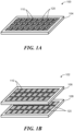
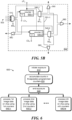
- a computational pixel imaging device 100 can include a substrate 104 on which is formed an array of detectors 110 and an array of pixel integrated circuits 120 that are arranged to receive signals from the corresponding detectors.
- a detector 110 and its corresponding pixel integrated circuit 120 can form a pixel of a computational pixel imaging device 100, and may both be located on a same substrate 104 in some embodiments.
- the arrays depicted in FIG. 1A are two-dimensional and may comprise tens, hundreds, thousands, or even millions of pixels when implemented in a device. In some cases, the arrays may be onedimensional ( e.g ., for a device that is scanned).
- FIG. 1B depicts an embodiment of a computational pixel imaging device 102 in which the detectors 110 are formed on a first substrate 106 in a detector array and the pixel integrated circuits 120 are formed on a second substrate in a pixel integrated circuit array.
- the detectors 110 on the first substrate 106 can be directly connected to receiving pixel integrated circuits 120 on the second substrate 108 ( e.g., by flip-chip or bump-bonding processes that may include solder bumps or posts).
- the detectors 110 on the first substrate 106 may be connected to receiving pixel integrated circuits 120 on the second substrate 108 through an interposer located between the substrates and not shown in the drawing.
- the interposer may provide some signal rerouting so that the array of pixel integrated circuits 120 on the second substrate may be larger than the array of detectors 110 on the first substrate. However, in some cases the pixel size for a pixel integrated circuit 120 may be the same or smaller than a pixel size for a detector 110.
- the first substrate 106 may be made from a first material that can be the same or different from a second material used to form the second substrate 108.
- the first substrate 106 may be made from a first semiconductor material (e.g ., indium phosphide (InP)) and the second substrate may be made from a second semiconductor material (e.g. , silicon (Si)).
- a first semiconductor material e.g ., indium phosphide (InP)
- the second substrate may be made from a second semiconductor material (e.g. , silicon (Si)).
- I-VI semiconductors such as cadmium telluride (CdTe) and mercury-cadmium telluride (HgCdTe)
- III-V semiconductors such as gallium nitride (GaN) and compositions including GaN, gallium arsenide (GaAs) and compositions including GaAs
- group IV semiconductors such as Si, germanium (Ge), or silicon-germanium (SiGe).
- detectors 110 may be used in a computational pixel imager 100, 102.
- the detectors 110 may comprise p-n or p-i-n junction photodiodes or phototransistors or photoconductors. Barrier detectors ( e.g ., barrier photodiodes, barrier phototransistors, etc .) may also be used in some cases and provide high detection sensitivity.
- the detectors 110 may comprise avalanche photodiodes for sensing low light levels.
- the detectors 110 may comprise microbolometers.
- the detectors 110 may be cooled to reduce background noise and/or to enhance responsivity of the detectors.
- the computational pixel imager 100, 102 may be mounted on a thermoelectric cooler or placed in thermal contact with a chilled heat sink or located in a dewer.
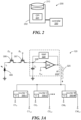
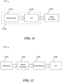
- a computational pixel imager 201 may be included in an imaging system 200 as illustrated in FIG. 2 , according to some embodiments.
- An imaging system 200 can include a camera 202 that may house collection optics 210 and a computational pixel imager 201.
- the imaging system 200 may also include a controller 250 that can connect to the camera 202 and computational pixel imager 201 by a wired or wireless data-communication link.
- the collection optics 210 may include one or more lenses and/or mirrors that act to form an image of a viewed scene on detectors 110 in the computational pixel imager 201.
- the detectors 110 may be located in an imaging plane of the collection optics 210 and an array of pixel integrated circuits 120 may be located in the imaging plane or adjacent to the imaging plane.
- some component(s) of the collection optics 210 may be moved controllably and automatically, the imager 201 may be moved controllably and automatically, and/or the entire camera 202 may be moved controllably and automatically ( e.g ., rotated by motors or actuators) to scan and image a large field of view.
- the imaging system 200 may be adapted as a visible imaging system, an infrared imaging system (e.g ., a night-vision system), an ultraviolet imaging system, or an x-ray imaging system.
- the choice of detector design and material can determine the responsivity of the detector to various wavelengths of radiation.
- Si-based photodiodes can be used for a visible imaging system (e.g ., wavelengths from about 380 nm to about 740 nm)
- CdTe photodiodes may be used for ultraviolet or x-ray imaging systems.
- indium arsenide or HgCdTe photodiodes may be used for an infrared imaging system.
- strained-layer superlattice detectors formed from III-V materials can be used for infrared imaging.
- detector design and material can be chosen to detect radiation within a spectral range that lies within a portion of an infrared wavelength range between 750 nm or approximately 750 nm and 5 microns or approximately 5 microns.
- a detector can be selected to detect radiation in an infrared spectral range between 0.75 micron and 3 microns or between approximately these end values.
- a detector can be selected to detect radiation in an infrared spectral range between 3 microns and 5 microns or between approximately these end values.
- the controller 250 can be implemented in various ways and forms.
- the controller 250 may be embodied as a field programmable gate array (FPGA), a mainframe computer, or anything in between such as a microcontroller, a microprocessor, one or more application-specific integrated circuits, a digital signal processor, a laptop computer or desktop computer, a tablet computer, a smart phone, etc.
- the controller 250 can be embodied as combinations of different controlling devices.
- Part of the control components can include code as software and/or firmware that adapts the controller 250 to execute functionalities that control operation of the imaging system 200 and receive, store, transmit, and process image data acquired by the camera 202.
- Controller components may also include custom logic and/or analog circuitry as well as memory that can be used by the computational pixel imager.
- the controller 250 may be configured to initiate the transfer of digital signals from the pixel integrated circuits 120 and to control the shifts, counts, and accumulation times that can permit the pixel integrated circuits 120 to perform digital-signal-processing functions on-chip.
- some control functions may be incorporated into the pixel integrated circuits 120 ( e.g ., hardwired or implemented as firmware). Such an integration may permit an array of pixel integrated circuits 120 to operate autonomously and perform on-chip, digital-signal-processing functions relatively free of external control.
- An imaging system 200 in accordance with the present embodiments may be used, for example, in industrial inspection, surveillance, process control, biological research, chemical research, pharmaceuticals, medical imaging, remote sensing, and astronomy.
- An implementation that comprises a computational pixel imager 201 and single-chip controller 250 may be incorporated in a variety of cameras, including portable, consumer, still and motion cameras, for example.
- a camera may be configured to operate in the visible region of the optical spectrum or in other wavelength regions by selecting appropriate detectors 110.
- a computational pixel imager 201 and controller 250 may be incorporated into a vision system for autonomous vehicles or robotic instruments.
- an imaging system 200 may be adapted for operation as an infrared camera and used for industrial sensing (e.g. , monitor heat emission from industrial components and/or machines), security, or firefighting, for example.
- An infrared camera may also be employed to provide an infrared image of a scene ahead of and/or around a vehicle.
- the imaging capability of the camera can extend beyond the human visible range of a scene illuminated by vehicle headlights.
- An acquired infrared image may be displayed, for example in a "heads up" display or overlaid on a windscreen of the vehicle to assist the vehicle operator. Potential hazards that are not visible to the unaided eye can become visible to a human operator through the camera and display.
- an imaging system 200 can include a cryogenically cooled infrared detector array, with connections between the detector array and the pixel integrated circuit array made via indium bump bonding, for example.
- the detector array may be suitable for low-light-level, low noise sensing in the infrared region of the spectrum (2-20 microns). Cooling may also be employed for detectors used in the visible and ultraviolet regions of the optical spectrum.
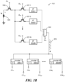
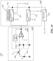
- a pixel integrated circuit 120 can include a first transistor 306, a capacitor C 0 , which may be included in a current-to-frequency converter 310, and at least one digital counter 330-1.
- a second transistor 307 may be included between the first transistor 306 and current-to-frequency converter 310.
- the second transistor 307 can provide additional isolation between node 308 or input to the current-to-frequency converter 310 and the source of the first transistor 306.
- the second transistor 307 connected in cascade, can help dampen noise arising from reset actions performed on node 308.
- the current-to-frequency converter 310 can be arranged to receive as input an analog signal and output a pulse every time a current exceeds a threshold value.
- the pulses can be counted by the counters 330-1, 330-2, ... 330-M.
- an area occupied by a pixel integrated circuit 120 may be approximately the same size or smaller than an area occupied by the detector.
- a voltage-to-frequency converter may be used instead of a current-to-frequency converter.
- a voltage-to-frequency converter may sense a voltage appearing on a node 308 of a capacitor C 0 and output a pulse every time a voltage exceeds a threshold value.
- a detector (which may be embodied as a photodiode 305) can generate a photocurrent I p when exposed to radiation.
- the detector (photodiode 305) may receive a stable bias from a bias source.
- biasing circuity can be included to apply a bias the photodiode 305 from a voltage source.
- the circuitry may include a large inductor on a bias line to block time-varying signals from the photodiode and pass a DC bias voltage. It may be advantageous to maintain a stable bias on the detector, and the second transistor 307 can help reduce bias variations that might otherwise occur due to resetting action at node 308.
- passage of the photocurrent I p to a capacitor C 0 of the current-to-frequency converter 310 may be controlled by the first transistor 306 (and/or second transistor 307) with the application of a digital control signal D in (and/or B in ), for example.
- the control signal D in (and/or B in ) may determine an exposure period for a pixel of the computational pixel imager. For example, when the control signal D in (and B in ) is at a logic "HIGH" or "1" level, photocurrent I p can flow and accumulate charge on capacitor C 0 raising the voltage at node 308.
- Toggling the first transistor 306 and/or second transistor 307 to a logic "LOW" or "0" level can block further photocurrent flow to the capacitor C 0 , and can terminate an exposure period.
- the exposure period can be repeated for video imaging and can be any suitable duration. In some embodiments, the exposure period may be any duration of time between 1 nanosecond (1 ns) for high levels of radiation on the detector and tens of minutes for low levels of radiation or for high-dynamic range sensing. Each exposure period can form an image frame with signals received from all pixels in the imager's array.
- the first transistor 306 (or transistors as described further below) may be used to provide gain and at least one of the transistors 306, 307 may be biased to operate in a sub-threshold region.
- the first transistor(s) may or may not be used to shutter an exposure period.
- shutter action for exposure periods can be accomplished by control signals (or clock signals) provided to the counters 330-1, 330-2, ... 330-M that instruct one or more counters when to start and stop accumulating counts.
- the input transistor(s) 306, 307 can be arranged as a switch (as in FIG. 3A ) for direct photocurrent injection, in some cases the input transistor(s) may be arranged in other configurations and two or more transistors may be used to receive photocurrent from the photodiode 305. For example, one or more transistors may be arranged to amplify a signal from the photodiode 305. Input transistor(s) may be connected as a source-follower, a transimpedence amplifier, or configured for buffered direct injection of the photocurrent I p .
- a current mirror circuit may be included in an input transistor arrangement, wherein the current mirror circuit provides current gain in a circuit branch that runs parallel to the branch containing the photodiode 305 and first transistor 306.
- the amplified current can be provided to the capacitor C 0 and current-to-frequency converter 310.
- the input transistor(s) 306, 307 are depicted as a field-effect transistor (FET), bipolar junction transistors (BJTs) and other types of transistors may be used in some embodiments.
- FET field-effect transistor
- BJTs bipolar junction transistors
- the capacitor C 0 may have one terminal connected to an output of the first transistor 306 (or second transistor 307, if present) and a second terminal connected to a reference potential (e.g ., ground as illustrated).
- the capacitance of capacitor C 0 can be small ( e.g., between 1 femtoFarad (1 fF) and 1 nanoFarad (1 nF). Higher or lower capacitance values may be used in other embodiments.
- capacitor C 0 can be embodied as parasitic capacitance of a discrete circuit device (e.g ., parasitic drain capacitance of the first transistor 306 or second transistor 307, if present), and may not be a separate discrete component in the integrated pixel circuit 120.
- the capacitor C 0 can determine the least significant bit value for a signal level from a pixel.
- FIG. 3A depicts one polarity for applying (sourcing) current to the current-to-frequency converter 310, in some cases it may be beneficial to reverse the orientation of the photodiode 305 or detector and sink current from the current-to-frequency converter 310.
- the use of appropriate types ( n -MOS or p -MOS) of transistors can allow a pixel integrated circuit to accommodate a current source or current sink photodetection strategy.
- Current applied to the current-to-frequency converter 310 may charge or discharge a capacitor C 0 .
- a reset of the capacitor may comprise applying a non-zero voltage to node 308, which can leave a potential across the capacitor C 0 that is discharged, at least in part, by subsequent exposure of the photodiode 305.
- the current-to-frequency converter 310 can include comparator circuitry 315 and reset circuitry 320, according to some embodiments.
- Comparator circuitry 315 can be embodied as a Schmitt trigger, comparator, or high-gain amplifying transistor that toggles between two output states: for example, from a low level to high, or high level to low, when an input voltage exceeds (or falls below) a reference voltage V ref .
- the reference voltage may be hardwired to a fixed value or may be a threshold voltage of a transistor.
- the reference voltage V ref may be programmable by an external control signal to two or more values.
- an integrated pixel circuit 120 may further include transistors (and resistive elements in some cases) arranged to provide programmable voltage values.
- Reset circuitry 320 may be embodied as one or more transistors arranged to discharge the capacitor C 0 (e.g ., shunt the capacitor's terminal connected to node 308 to the reference voltage connected to the other terminal of the capacitor. For example, a toggling of an output from the comparator circuitry 315 can activate the reset circuitry 320 to discharge the capacitor C 0 , which can cause the comparator circuitry 315 to toggle back to a prior state of the two states.
- the current-to-frequency converter 310 may be embodied as described in connection with figure 3 of U.S. patent No. 10,348,993 , the entire contents of which is incorporated herein by reference.
- an output of pulses 325 can be provided to one or more counters 330-1, 330-2, ... 330-M during an exposure period.
- the number of pulses during an exposure period will depend upon and be proportional to an amount of radiation incident on the detector (photodiode 305 in the illustrated embodiment). A higher level of radiation will produce a larger number of pulses during the exposure period.
- One or more of the counters 330-1, 330-2, ... 330-M can accumulate counts for the pulses received during the exposure period. At the end of the exposure period, the number of counts can be read out of a counter as a digital signal level for the pixel. The digital signal level will be indicative of an intensity of radiation received by the detector at the pixel.
- the counters 330-1, 330-2, ... 330-M can be implemented with transistors arranged as logic gates, according to some embodiments.
- a counter can be formed from flip-flop logic circuits and embodied as an N-bit ripple counter. Other types of counters, such as synchronous counters may also be used in some implementations.
- Accumulated counts may be output over parallel digital data lines C1 out , C2 out , ... CM out .
- count values from the counters can be provided to shift registers that are connected to each counter.
- the shift registers may also be located in the pixel and form part of the pixel integrated circuit 120.
- the counters themselves are configured for additional use as shift registers.
- a counter's bit size can determine the most significant bit limit on signal values from a pixel.
- the counters 330-1, 330-2, ... 330-M are programmable over digital input lines C1 in , C2 in , ... CM in .
- the counters may be programmed to increment or decrement counts at the start of each exposure period.
- counting direction may be changed by a programmable control signal at any time during an exposure period.
- the counters may be programmed with an initial count value for the start of each exposure period.
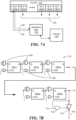
- Embodiments described herein are not limited to one current-to-frequency (or voltage-to-frequency) converter per pixel. Two or more converters may be used per pixel integrated circuit 122, as illustrated in the example of FIG. 3B .
- one or more pixels of a computational pixel imager can include two or more current-to-frequency converters 310-1, 310-2, ... 310-N arranged to receive an output from the pixel's detector (photodiode 305 in the illustrated example).
- the N second transistors can be used to provide added isolation of the pixel's detector from resetting actions occurring in the current-to-frequency (or voltage-to-frequency) converters. Additionally, the N second transistors 307-1, 307-2, ... 307-N can be used to select one or more of the converters 310-1, 310-2, ... 310-N for processing of the signal from the photodiode 305.
- the converters can be as described above in connection with FIG. 3A , and their description need not be repeated.
- outputs from the converters 310-1, 310-2, ... 310-N may connect to a multiplexer 340 that can be controlled with a digital input signal M in applied to a control port.
- the control signal M in can select which input port connects to an output port of the multiplexer.
- the multiplexer 340 can be a N:1 multiplexer.
- FIG. 3B illustrates an example case in which the pixel's counters 330-1, 330-2, ... 330-M can be shared by (e.g., dynamically assigned to) any of the converters 310-1, 310-2, ... 310-N.
- a multiplexer 340 may not be used for some or all converters and one or more of the converters may have separate counter(s) that are dedicated or statically assigned to each converter.
- Other circuit arrangements are also possible. For example, a first group of counters or a single counter in a pixel may be dedicated to one converter or shared by a first group of converters, and a second group of counters or a second single counter in a pixel may be dedicated to one converter or shared by a second group of converters.
- Adding additional converters can provide redundancy in pixels and improve fabrication yields. For example, if one of the converters fails in a pixel due to microfabrication processes, another converter can be selected for the pixel so that all pixels in the array of pixel integrated circuits can be used.
- the converters 310-1, 310-2, ... 310-N within a pixel can be configured differently (to exhibit different gain, frequency characteristics, power consumption, capacitance value for capacitor C 0 , etc. This can provide improved coverage with the same computational pixel imager for different signal conditions and operating conditions including but not limited to gain, noise, power, and maximum detectable frequency modulations.
- Adding additional converters and counters can also support multi-thread processing operations described herein.
- a signal from a pixel's detector e.g. , photodiode 305
- Some of the functional operations can include bit operations such as, but not limited to, add, subtract, complement, shift, compare, and rotate.
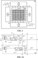
- FIG. 4 depicts some additional data-handling circuitry that can be included with a computational pixel imager.
- a computational pixel imager 100, 102 may include circuitry that permits the orthogonal transfer of accumulated counts on counters throughout the array 406 of pixel integrated circuits. The orthogonal transfer of count values can be accomplished by shifting count values from a pixel's counter(s) to any one of the pixel's four nearest-neighbor pixels' counters, as described further below.
- each shaded rectangle 402 within the array 406 depicts approximately an area occupied by a pixel, though in an actual device there can be thousands to millions of pixels.
- digital counts can be transferred through column-transfer data lines 420 and/or through row-transfer data lines 430 to other pixels or to the data handlers 410, 412, 414, 416.
- multiplexers can be included to serialize data from multiple column-transfer data lines 420 and/or row-transfer data lines 430 that is sent to the data handlers 410, 412, 414, 416 and/or off chip.
- one or more M: 1 multiplexers (where M can be any integer value of 2 or greater) can be used to serialize data from multiple row-transfer data lines 430 onto single data lines that provides pixel data to one or more of the data handlers.
- any result or count value from a counter within the array 406 may be transferred to another counter in a different pixel within the array 406 or to the data handlers.
- Such transfer capability along with programmability of the counters (increment, decrement) and control of count accumulation times can allow digital signal processing operations to be performed within the array 406.
- Digital signal processing operations that may be performed within the array can include, but are not limited to, threshold filtering, high-pass filtering, low-pass filtering, edge-detection filtering, match filtering, spatial filtering, temporal filtering, or spatio-temporal filtering, smoothing, differentiation, data compression, time-domain integration, image correlation, and convolution.
- match filtering may be implemented by developing a filter kernel for cross correlation with objects in an imaged scene (e.g., a person's iris in a personal identity system, a facial image, a target object).
- Convolution of a kernel with an image can be implemented as a series of count accumulations (which may increment and decrement counts) and counter value orthogonal transfers.
- a correlated or convolved image can then be thresholded by compare logic for detections (e.g ., detection of an iris or target object).
- Data transmitted from the array could be raw cross-correlation or convolution results, or may be only data associated with the detections alone which could reduce the amount of data transmitted and subsequently processed.
- a signal from a steering and/or motion-sensing mechanism may be used to shift accumulated counts in an array synchronously with the overall motion of an imaging system to enable time-domain integration. Similar control of shifting counts can also enable image stabilization for environments where the imaging system may undergo unwanted vibrations.
- non-uniformity correction for an imaging array may be performed by counting down for a frame period while viewing a flat, extended source (e.g., a mechanical shutter). After the background scene is acquired, the counters can be configured to count up while the scene data is acquired. After a frame period, only signal and noise data will be present and any systematic non-uniformity of the imager will be cancelled.
- Non-uniformity correction may employ a 50% duty cycle for scene and background image acquisition.
- data serializers may be included in each pixel integrated circuit to send count values from multiple counters within the pixel serially over a signal row and/or column-transfer data line.
- Data handlers 410, 412, 414, 416 may comprise additional transistor circuitry that is configured to provide additional data-processing operations and/or control of data transfer and programming of the pixel integrated circuits 120.
- data handlers 410, 412, 414, 416 may include additional registers and data serializers to read data from and onto row and column data-transfer lines 430, 420.
- Data handlers 410, 412, 414, 416 may also include logic gates to enable control of the exposure period duration, counter direction, and/or threshold voltage reference V ref .
- data handlers can be configured to perform threshold detection, compare, match filtering, and data selection functions.
- data handlers can be configured to determine a read-out time for selected rows and/or columns (as may be used in connection with infinite dynamic range pixels described below, for example).
- Data handlers 410, 412, 414, 416 may also include input/output data lines I / O 1 , I / O 2 , I / O 3 , and IlO 4 that can be used to send processed or unprocessed signals, for example, to an external analyzer or processor for further data processing and analysis.
- one or more of the data handlers 410, 412, 414, 416 may be located on a same chip as the array 406 of pixel integrated circuits.
- one or more of the data handlers 410, 412, 414, 416 can be located on a different chip that is connected to the chip containing the array 406 of pixel integrated circuits.
- the array 406 of pixel integrated circuits and data handlers 410, 412, 414, 416 can be manufactured using complimentary metal-oxide-semiconductor (CMOS) microfabrication processes.
- CMOS complimentary metal-oxide-semiconductor
- FIG. 5A illustrates one example of how multiple counters 530-1, 530-2 in one pixel 502 of a computational pixel imager may be connected to counters in adjacent pixels.
- a pixel can include more than two counters in some implementations. Additional counters can be connected in a same way to counters in adjacent pixels.
- the counters can be ripple counters, though other types of counters can be used in other embodiments.
- counters may be implemented with D flip-flops for each bit and the flip-flops can be connected in series with an output of one flip-flop connected to an input of a next flip-flop. Further details of counters and associated circuitry that can be used in the implementations depicted in FIG. 5A and FIG. 5B can be found in U.S. patent No. 9,768,785 as described in connection with Figure 3 and Figure 4 in that patent, which is incorporated herein by reference in its entirety.
- multiple counters are connected to neighboring counters in a way such that counters operated in a particular manner for image acquisition or performing a signal-processing function can shift count values to other counters anywhere in the array that are operated in the same manner.
- the shifting of counter values may be through nearest neighbor shifts. For example, a first counter 530-1 operated in a first manner in a first pixel 502 may shift its count value to a first counter operated in a same manner in a first nearest neighbor pixel, whereas a second counter 530-2 operated in a second manner in a first pixel 502 may shift its count value to a second counter operated in a same manner in a second nearest neighbor pixel.
- the first nearest neighbor pixel can be the same or different than the second nearest neighbor pixel.
- An example of a first manner of counter operation may be raw image acquisition where the corresponding first counters continuously count up during an exposure period.
- An example of a second manner of counter operation may be temporal filtering to detect changes in pixel values by modulated signals or moving objects where a count value is incremented for half an exposure period and then decremented for half an exposure period. Other manners of counter operation are possible as described above and below. By repeated nearest neighbor shifts, along rows and columns, a value on one counter can be shifted to another corresponding counter anywhere in the array.
- the counters can be configured to function as both counters and shift registers. Further counter values from multiple counters 530-1, 530-2 in a pixel 502 can be passed over separate data lines (e.g., row data-shift lines 551-2, 552-2) to multiple corresponding counters in an adjacent pixel. Counter values can be passed to adjacent pixels in either direction within a row or column along different data-shift lines (e.g ., data-shift lines 551-1, 551-2, 551-3, 551-4). The data-shift lines may also be referred to as row or column buses. Additionally, counter values for pixels at an edge of the array can be passed to edge logic for read-out and/or data processing via the data-shift lines.
- the data-shift lines may be parallel data lines (such that count values are passed in parallel) or serial data lines.
- b:1 multiplexers for b-bit counters may be included in the pixel after the counter output to place count values serially onto data-shift lines.
- shift multiplexers 540-1, 540-2 can be included in each pixel, connected to counter outputs, and controlled by signals applied to inputs M1 in , M2 in from edge logic to direct counter values to one of the neighboring pixels.
- input multiplexers 510-1, 510-2 can be connected to data inputs of the counters 530-1, 530-2 to receive and place count values from neighboring pixels' counters on counters 530-1, 530-2 within the pixel.
- Input multiplexers 540-1, 540-2 may also be controlled by signals applied to inputs M3 in , M4 in from edge logic.
- values from multiple counters within a pixel can be multiplexed onto a same row or column data-shift line with counter-output multiplexers 560.
- the counter-output multiplexers 560 can be M: 1 multiplexers, where M is an integer value of 2 or greater and corresponds to the number of independently controlled counters within the pixels.
- data received from adjacent pixels can be received by a single input multiplexer 510.
- the input multiplexer 510 can be a 4:M multiplexer, where M is an integer value of 2 or greater and corresponds to the number of independently controlled counters within the pixels.
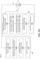
- FIG. 6 illustrates an example method of multi-thread processing 600 that can be performed with an array 406 of pixel integrated circuits having multiple programmable counters in each pixel and arranged to shift values to counters in adjacent pixels as described above.
- a method 600 can include acts of initiating (act 610) an exposure of a detector array of a computational pixel imager to generate image data.
- an exposure period e.g., a signal acquisition period that can be used to form an image frame
- multiple counters in each of a plurality of pixels can accumulate (act 620) count values.
- the count values for at least some of the counters can be accumulated independently of count values accumulated by other counters and can differ from count values accumulated by other counters, even within a same pixel.
- the counters within a same pixel can be programmed to operate differently. For example, two counters within a pixel may be programmed to increment and decrement counts periodically at a same frequency but with phases shifted by 90 for in-phase and quadrature (I-Q) detection of a modulated optical signal whereas a third counter can be programmed to increment counts for one-half of an exposure period and to decrement counts for one-half of an exposure period to detect non-stationary objects in an imaged scene. Accumulation of counts in counters can terminate when and exposure is terminated (act 630) ending the exposure period.
- I-Q in-phase and quadrature
- one or more counters within a pixel can be programmed to accumulate counts in response to exposure of the pixel's detector, whereas one or more other counters within the pixel can be programmed to perform other operations on data previously accumulated or provided to the counter(s) (e.g ., shift operations, bit rotation operations, ones complement, addition, subtraction, compare, read-out, data receive, etc .)
- Such different in-pixel operations on the counters can be in response to multiple threads that execute simultaneously on the system.
- first image data (first counter values) acquired with first counters from the pixels can be processed (act 640-1) using shift operations and/or any of the above counter operations to perform a first signal-processing function (e.g ., spatial filtering).
- second image data (second counter values) acquired with second counters from the pixels can be processed (act 640-2) using shift operations and/or any of the above counter operations to perform a second signal-processing function (e.g ., temporal filtering).
- the different signal-processing functions can be performed, at least in part, while count values are being accumulated in a subsequent exposure period (as may be the case for convolution, correlation, time domain integration for a deterministically moving camera, or image stabilization functions).
- raw count values may be accumulated as new image data on one or more counters in a pixel while signal processing operations are being performed with other counters, such that the computational pixel imager has essentially no dead time in imaging a scene or successive scenes.
- the multiple execution threads (acts 640-1, 640-2, ... 640-N) can execute simultaneously.
- the multiple execution threads can execute simultaneously.
- at least some signal-processing operations for different counters performing different functions can occur at a same time (e.g., on same clock cycles that drive data transfer or arithmetic operations).
- outputs and inputs of multiple counters are connected across pixels using multiplexers to serialize counter data onto shared data-shift lines as illustrated in FIG.
- At least some signal-processing operations for different counters performing different functions may be interleaved in time and occur on alternating clock cycles.
- multiple execution threads (acts 640-1, 640-2, ... 640-N) can execute concurrently on a pixel integrated circuit chip.
- data for the corresponding counters can be read out of the array 406 of pixel integrated circuits over column-transfer data lines 420 and/or row-transfer data lines 430 for display, analysis, storage, and/or further signal processing.
- a computational pixel imaging device 100 of the above-described embodiments can include counters that are configured for infinite dynamic range sensing.
- the dynamic range of an image sensor describes the difference between the brightest and dimmest object that can be detected and discerned in an image.
- Conventional digital imaging approaches typically cannot achieve high dynamic ranges over three or four orders of magnitude, for example. Digitizing in-pixel, as is done for a computational pixel imaging device 100, can improve the dynamic range capability over conventional digital imaging sensors.
- digitizing in the pixel for high dynamic ranges presents challenges when trying to implement with small pixel sizes. To achieve a high dynamic range, the size of counters must be increased.
- CMOS process node may be used to reduce transistor and counter size, but such advanced microfabrication processes may be prohibitively expensive in some instances.
- Other approaches to reducing the size of digital-pixels e.g ., to the 10 ⁇ m size or smaller is desirable to reduce the size, weight, and power (SWaP) of imaging sensors and imaging devices.
- SWaP size, weight, and power
- the inventors have recognized and appreciated the finite-bit counters (e.g., an 8-bit counter) can be configured for unlimited dynamic range.
- circuitry for an infinite dynamic range counter 710 is depicted in FIG. 7A , according to some embodiments.
- circuitry for an infinite dynamic range counter 710 can include a b -bit counter, read/store logic 730 that is in communication with the counter, and memory 750.
- the counter 710 can comprise any type of counter described above, such as a ripple counter or synchronous counter or other types of counters.
- the read/store logic 730 may be embodied as processing logic that could be located on-chip or off-chip and that is configured to determine when to read the most significant bit or group of most significant bits of one or more counters of a computational pixel imaging device 100 and store in memory 750 information indicating that counters have rolled-over in count value one or more times.
- read/store logic 730 can be implemented as on-chip logic gates or field-programmable gate arrays located within each pixel, or located at an edge of an array 406 of pixel integrated circuits ( e.g., in one or more of data handlers 410, 412, 414, 416 referring to FIG. 4 ).
- an infinite dynamic range counter 710 can comprise a b-bit counter in which the most significant bit (MSB) 720-b is interrogated differently than the lower bits 720-1, 720-2, ... 720-a.
- the size of the counter (value of b) can be any integer value of 2 or greater. In some implementations, the size of the counter is between 3 bits and 25 bits, though larger counters may be used in some cases.
- the MSB 720-b is interrogated at a higher read-out rate than the lower bits. For long exposure periods and/or high signal levels, counters in some pixels can reach their maximum count value and roll-over to a value of 0 and continue counting up. If the roll-over is undetected, signal information is lost.
- a group of MSBs may be a counter's MSB and the next N lower bits (e.g., bits b, b -1, b -2, ... b -N) where N is a positive, non-zero integer.
- outputs from counters can be connected in parallel across corresponding counters in an array 406 of pixel integrated circuits, as described above in connection with FIG. 5A or FIG. 5B .
- bit values for counters may be connected in parallel across corresponding counters in an array 406.
- the data-shift lines may comprise parallel data lines 730, 740 with the number of parallel data lines equaling the number of counter bits. Additional multiplexers may be used for each of the parallel data lines.
- a MSB from each counter in a row or column may be connected to a same data-shift line.
- values of MSBs can be read from shared data-shift lines using a synchronous cadence read-out, for example.
- the counter may be configured to pass bits between each counter unit that is used to record a bit, as depicted in FIG. 7B , for example, for as described in U.S. patent No. 9,768,785 .
- bit values for counters may not be connected in parallel across corresponding counters in an array 406. Instead, bit values may be shifted sequentially onto a same data-shift line.
- an infinite dynamic range counter can work as follows. While counters accumulate count values during an exposure period, the values (logic levels) of the counters' MSBs (or groups of MSBs) can be read and monitored by read/store logic 730 over MSB data lines 740. In some implementations, when a counter's MSB toggles to a logic 1 state (or group of MSBs toggle to a predetermined value), the value may be signaled to and/or detected by read/store logic 730 by placing the value on one or more data lines (e.g ., placing a MSB's value on data line 740).
- a bit's value may be placed on a data line 740 by in-pixel logic, such as an AND gate, for example).
- all MSB bit values (or groups of MSBs values) for all counters in the array 406 may then be destructively read out so that the MSB values that have toggled to 1 (or a predetermined value) are read and reset to 0.
- a toggling of the MSB (or group of MSBs) can indicate a roll-over of the b-1 bits (or b-N -1) and an upcoming roll-over for the b -bit counter.
- a record of a counter's toggling or roll-over and address can be stored in memory 750 by the read/store logic 730.
- the address can be determined from the read address used to access the counter when all counters in the array are read or all counters in a row or column are read. In some cases, the address may be determined based upon clock cycles used to read counters in a row and/or column.
- Read/store logic may reset counters' MSB value(s) over control lines ( e.g ., control line 742). The counters are then allowed to continue accumulating count values until a next MSB or group of MSBs toggles.
- the number of togglings or roll-overs for each counter can be accumulated in memory 750, where each toggling represents a count of 2 ( b -1) (or 2 ( b - N -1) ) .
- roll-over events may be detected by detecting a logic 0 level, or by inverting the MSB output and detecting a logic 1 level.
- in-pixel logic or edge logic may be configured to detect, for example, a falling edge or negative edge of the b th bit.
- a monitor flip-flop may be configured to latch a logic 1 value to its output when the MSB value rolls over from 1 to 0. Additional in-pixel logic may assert output of the monitor flip-flop on a data line that can be detected and read. The monitor flip-flop can then be reset to detect a next falling edge of the MSB. In such embodiments, each detected logic 1 level from the monitor flip-flop indicates 2 b counts and the MSB does not need to be reset.
- time-gated row and column monitoring may be performed by read/store logic to detect and determine the location and address in the array 406 of a counter whose MSB value has toggled, and only that counter (or monitor flip-flop) will be destructively read.
- read-out times of counters' MSB values may be predicted based on prior count accumulations. For example, a first exposure over a first time period may be performed for a short duration in which none of the counters' MSB values roll over. First count values can accumulate on the counters during this exposure period.
- times for reading and resetting MSB values from one or more counters may be determined from the ( b - 1 ) th bit value (or other bit's value) of a relevant counter in the array. For example, when the ( b - 1 ) th bit value (or other bit value) of a first counter in the array toggles to a logic 1 level and the duration of the exposure period is known, a count rate for the counter can be determined.
- the count rate can be used to predict, on a subsequent longer exposure, when the counter's MSB value will toggle to a logic 1 level, e.g., and must be read ( e.g., accumulate a roll-over count in memory 750) and/or reset. Accordingly, the count rates for all counters in an array 406 can be determined and used to predict when one or more counter's in the array will roll over. The information can then be used to determine, for longer exposures of a same scene, when to read the MSBs of the counters, either globally (reading all counters' MSBs sequentially in a read-out) or individually.
- the duration of the first exposure may be estimated based on prior images, or several exposure periods may be tried and linearity of increasing counts between at least two successive exposures checked to determine whether any of the counters have rolled over. If all counters have increased linearly or nearly-linearly in two successive exposures, then either exposure results may be used to estimate when roll-overs could occur.
- a first exposure's duration may be determined and terminated automatically.
- a counter's MSB value may be asserted on a row or column data-shift line as soon as the MSB toggles to a logic 1 level. The value may be asserted by in-pixel logic. Edge logic may detect the logic level and terminate the exposure period.
- Read/store logic 730 may then read-out all counters and process their count values to determine count-accumulation rates for each counter. The count-accumulation rates can then be used to determine when to read MSB values from one or more counters during a subsequent longer exposure period of a scene during which at least some counters' values would roll over.
- each counter may be divided equally or unequally into two bit groupings and each grouping may be used to accumulate counts.
- the bit groupings may be read at different times and total counts accumulated in memory located outside the array of pixels. For example, a first of the two bit groupings (e.g., bit 1 to bit ( b-N- 1)) can be read and reset at a first time, and subsequently the second of the bit groupings (bit b-N to bit b ) can be read and reset a second time, and the process repeated multiple times during an exposure period for an image.
- the reading and resetting may alternate between the two bit groups for each successive read.
- the read and reset rates may differ for the two groups.
- the read and reset rate for a bit group may be determined by any of the above-described methods for an infinite dynamic range counter.
- additional operations may be executed on count accumulations that have been recorded in memory 750. For example, when on-chip data processing or data-shift operations occur (such as for filtering), then such operations can be mirrored or complied with using the count accumulation data in memory. For example, if counter values are shifted in the array 406 of a computational pixel imager, then addresses associated with off-array count accumulations may be updated to reflect the on-array shift of counter data.
- a b-bit counter 710 may be configured as series-connected D or JK flip-flops 725-1, 725-2, ... 725-a, 725-b with reconfigurable data inputs D and reconfigurable clock inputs CLK.
- Each flip-flop can be used to store one bit.
- the flip-flop clock inputs can be reconfigured on-the-fly, so that the series of flip-flops operates as a ripple counter. For example, pulses 325 from the current-to-frequency converter 310 (referring to FIG.
- each flip-flop 3A can be applied to the clock input of the first flip-flop 725-1 (least significant bit) and used to toggle the output of that flip-flop.
- the output of each flip-flop may then drive the clock of the next flip-flop to form a ripple counter.
- the clocks of each flip-flop may be connected to a same read-out clock and the data inputs D connected to the data outputs Q of the preceding flip-flop, so that data can be shifted across and out of the counter 710.
- a tri-state buffer 770 may be used to place the output value Q of the flip-flop 725-b corresponding to the MSB on a data line 740, as illustrated in FIG. 7B .
- additional tri-state buffers may be used for other flip-flops.
- an AND gate 775 (or analogous logic circuitry) can be used to monitor the output of the MSB flip-flop 725-b and activate the tri-state buffer 770 when the MSB toggles to a logic 1 level.
- the data line 740 may be a separate and dedicated data line for monitoring only the value of the MSB (e.g., separate from a data line that is used to read out the entire counter value or to provide orthogonal shifting of counter values in the array 406). In other implementations, the data line 740 may be a same data line that is used to read out the entire counter value or to provide orthogonal shifting of counter values.
- Counters configured for infinite dynamic range counting may be included in computational pixel imagers having multiple counters in each pixel as described above ( e.g., for multi-thread signal processing). Counters configured for infinite dynamic range counting may also be included in computational pixel imagers configured for down-sampling of modulated signals, as described below in connection with FIG. 9 .
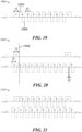
- Example read-out rates for MSB values are plotted in FIG. 8 for various count accumulations rates from 1 MHz to 20 MHz and counter bit depths.
- the plotted MSB read-out rates correspond to rates required to avoid missing a roll-over event.
- the lines of count accumulations rates are, from top to bottom, 20 MHz, 10 MHz, 5 MHz, 2 MHz, and 1 MHz.
- Counters may roll over multiple times during a high-dynamic range exposure period, and the number of roll-over events for a counter accumulated in memory 750.
- the number of roll-over events stored in memory 750 are in quanta of 2 (b-1) counts.
- the number of counts for a counter indicated in memory 750 are combined with the final count value for the counter to obtain the total number of counts.
- pixel integrated circuits 120 (which can include multiple counters as describe above and/or infinite dynamic range counter circuitry) can be configured for digital pixel down-sampling in some implementations.
- the phase of amplitude-modulated light returned from an object can contain information regarding the distance of the object from the observer. In-pixel digitization with two counters may be used to determine phase of amplitude-modulated light.
- the two counters can be controlled to cyclically count up and down at a same frequency as the modulated source, but one counter's phase is shifted by 90o with respect to the other counter (e.g ., in-phase and quadrature detection).
- a limitation of using amplitude-modulated light to measure distance is that relatively high modulation frequencies (e.g., MHz to GHz frequencies) may be needed to achieve high distance resolution.
- the use of high modulation frequencies can challenge the ability of current-generation, up/down counting, digital-pixel electronics.
- the power requirements for detecting high-frequency modulations can be unacceptably high for some embodiments.
- apparatus and methods can be employed to adapt sensors of computational pixel imaging devices to downsample the modulated signals so that relatively low frequency up/down counters can be used to detect phases of modulated signals at much higher frequencies.
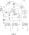
- FIG. 9 illustrates an example of a pixel integrated circuit 920 adapted for digital down-sampling.
- the pixel integrated circuit may be used in pixels of a computational pixel imager and contain the same components as for the pixel integrated circuit 120 described above in connection with FIG. 3A , which will not be described again and are given same reference numbers.
- a detector 905 of a computational pixel imager may be adapted to be biased with a modulated supply 910 that can provide, for example, a modulated bias or supply voltage to the detector.
- the modulated supply 910 may be located off-chip and provided to one or more pixels' detectors via bias lines.
- the detector 905 may be a p-n junction photodiode in some embodiments or may be a phototransistor, as illustrated in the drawing.
- the object 904 can be in a field of view that is imaged onto an array of detectors in a computations pixel imager.
- the light source 902 may comprise a laser, one or more laser diodes, one or more light-emitting diodes, etc. that is (are) driven by a second modulated supply 912. Modulated light can be returned (scattered or reflected) from the object 904 and detected by the modulated detector 905.
- one or both of the modulated supplies 910, 912 can be included with either or both of an array of pixel integrated circuits 120 or an array of detectors 110. In some implementations, one or both of the modulated supplies 910, 912 can be included in a computational pixel imaging system. In some cases, a computational pixel imaging system may be provided without the supplies 910, 920, but may have modulation inputs configured to receive one or both of the modulation signals from modulated supplies 910, 920.
- one of the frequencies f 1 or f 2 may be derived from the other (e.g., by using a mixer that mixes f 1 with a signal from a source operating at the difference frequency ⁇ f ).
- a computational pixel imager may include one or both of the difference-frequency source and high-frequency source. Further, an output from the difference-frequency source can be used to drive count-up and count-down cycles of one or more counters instead of an output from a mixer.
- the difference ( ⁇ f ) between the two modulation frequencies f 1 , f 2 can be significantly smaller than the value of either frequency.
- the difference can be tens or hundreds of kilohertz (e.g., between 10 kHz and 500 kHz) whereas the modulation frequencies can be in the megahertz to multi-gigahertz range.
- Modulation of the bias on the detector can change the sensitivity of the detector and/or effectively gate the detector on and off.
- the detector 910 can then act as a mixer and demodulate the received modulated optical signal so that the counters 330-1, 330-2, ... 330-M can detect at the difference frequency ⁇ f.
- the first and second frequencies f 1 , f 2 can be provided to a mixer 915 (which may be included with a computational pixel imaging system). An output from the mixer can be used to generate a clock signal with clock generation circuitry 917. The generated clock signal may determine the periodicity of count-up and count-down cycles of one or more of the counters 330-1, 330-2, ... 330-M.
- a benefit to this technique is that pixel and device power can remain low while still measuring the return phase of a reflected signal.
- an optical element (lens, diffractive optical element, etc .) can be placed in front of the optical source 902 to project a pattern of light onto the object.
- the pattern may be, for example, an array of spots or lines. Distortion of the pattern and/or distances to each portion of the pattern can be detected with a computational pixel imager, even though returned light from the pattern may be dim or not visible to the naked eye due to other illumination of a field of view. Analysis of the pattern distortion can be used to determine three-dimensional geometry of the object as well as one or more distances to the object.
- a computational pixel imaging device for example, the computational pixel imaging device 100 of the above-described embodiments can be adapted for event-based imaging .
- a pixel integrated circuit can be configured to detect changes in received light intensity and return a null signal or not report a signal when no changes are detected.
- a meaningful change in detected light intensity e.g ., a change greater than a predetermined amount or threshold value
- Such changes may be of interest in certain imaging applications (e.g ., to emphasize detection of moving objects in an imaged scene).
- a computational pixel imaging device adapted for event-based imaging can provide event images, each of which may include data about multiple events detected by pixels in an array during an image acquisition period, which may include an exposure period as described above.
- An image acquisition period for a computational pixel imager may comprise time associated with signal acquisition ( e.g ., during an exposure period) and time associated with on-chip signal processing to prepare image data for read out.
- the data associated with each event in an event image may indicate the address of the pixel that detected the event and/or the magnitude of the change detected by the pixel.
- only data associated with pixels that have detected an event may be transmitted for further processing rather than an entire frame of data containing information from every pixel in an imaging array.
- An event-based computational pixel imaging device that transmits sparse pixel data, at least part of the time, can reduce latency and power, and improve data rate and dynamic range over conventional event-based vision devices.
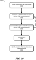
- FIG. 10 illustrates an example method 1000 of event-based imaging that can be performed with an event-based computational pixel integrated circuit, according to some embodiments.
- An event-based computational pixel integrated circuit may be configured similarly to the pixel integrated circuit 120 as described above with respect to FIG. 3A .
- the event-based computational pixel integrated circuit may include the first transistor 306 or input transistors 306, 307 and the current-to-frequency converter 310 that includes the capacitor C 0 .
- the event-based computational pixel integrated circuit may further include at least one digital counter configured for event-based imaging. Like the counters 330-1, 330-2, ... 330-M illustrated in FIG.
- At least one digital counter configured for event-based imaging may be arranged to receive as input the pluses 325 from the current-to-frequency converter 310. Different from the counters 330-1, 330-2, ... 330-M, at least one digital counter configured for event-based imaging may provide an output by performing at least a portion of the acts of the method 1000.
- At least one digital counter configured for event-based imaging may be capable of operating in multiple modes including, for example, a normal imaging mode and an event-based imaging mode.
- the mode that the counter operates in may be triggered by a control signal from, for example, the controller 250 and/or the data handlers 410, 412, 414, 416.
- the counter In the normal imaging mode, the counter may count in a single direction, for example, either incrementing counts or decrementing counts, during an exposure period like the counters 330-1, 330-2, ... 330-M such that a digital number output by the counter indicates the intensity of radiation captured by a detector coupled to the counter (e.g., a photodiode 305).
- the counter may count in two opposite directions during an exposure period by, for example, performing at least a portion of the acts of the method 1000 as described below, such that a digital number output by the counter indicates whether an event has been detected by the detector coupled to the counter. Additionally, the resulting count can also indicate the magnitude of the detected event.
- the method 1000 may include acts of initiating (act 1010) an exposure of a detector array of an event-based computational pixel imager to generate an event image.
- the counter configured for event-based imaging may accumulate counts by incrementing (act 1020) a digital number on the counter in response to a received signal 325.
- the counter configured for event-based imaging may continue accumulating counts by decrementing (act 1030) the digital number on the counter in response to a received signal 325. It should be appreciated that there may be no delay between the act 1020 and the act 1030 for high speed and low latency imaging.
- a continuous counting in opposite directions during an exposure period enables the pixels to indicate a detected change when the resulting digital number has a non-zero value and/or exceeds a threshold level or is outside a range of values.
- the threshold level (or range of values) may correspond to a noise floor.
- the value of the digital number may also indicate a magnitude of the detected change. In some cases, the magnitude may be a magnitude above a noise floor.
- the digital number after the act 1020 is not reset to an initial count value before the act 1030.
- the present application is not limited to the illustrated order of act 1020 and act 1030.
- the counter configured for event-based imaging may be configured to decrement a digital number and then increment the digital number.
- the first and second portions of the exposure period may be divided into sub-portions.
- the counter configured for event-based imaging may be configured to switch between incrementing and decrementing a digital number between the sub-portions, without resetting or otherwise processing the digital number between the sub-portions of the exposure period.
- the acts of incrementing and decrementing counts can be repeated multiple times during an exposure period, prior to ending (act 1040) exposure for the event image.
- the lengths of the first portion and the second portion of the exposure period may be determined such that a pixel capturing a stationary object returns a zero and a pixel that has detected a change returns a non-zero value.
- the first portion and the second portion of the exposure period may be proportioned such that background noise is removed and a pixel capturing a stationary object returns a zero.
- the first portion and the second portion of the exposure period may be of a same duration (e.g., one half of the exposure period, one-quarter of an exposure period, one-twentieth of an exposure period, etc .).
- An advantageous aspect of the computational pixel imager is that the incrementing and decrementing portions can be programmed to any suitable value. Smaller values can allow for event detection of more rapidly changing events. For values less than one-half an exposure period, the incrementing and decrementing portions can be repeated multiple times during an exposure period.
- the method 1000 may include ending (act 1040) the exposure for the event image.
- the method 1000 may include identifying (act 1050) pixels of the array that have detected events. Identification of pixels that have detected events can be performed by, for example, logic circuitry.
- the logic circuitry and the event-based computational pixel imager may be on different substrates, or a same substrate. In some cases, the logic circuitry can be included in each pixel integrated circuit of a computational pixel imager.
- FIG. 11 depicts an example of an event-based computational pixel imaging system 1110 according to an embodiment of the invention. which may include an event-based computational pixel imager 1108.
- the event-based computational pixel imager 1108 includes a pixel array 1102 configured for event-based imaging as described above, and an input/output circuitry 1104 configured to read out the digital numbers of all pixels in the pixel array 1102 after individual image acquisition periods.
- the event-based computational pixel imaging system 1100 includes logic circuitry 1106 configured to receive the digital numbers from the event-based computational pixel imager 1108.
- the logic circuitry 1106 may be implemented in any suitable manner including, for example, a microprocessor, a microcontroller, a field-programmable gate array (FPGA) and an application-specific integrated circuit (ASCI).
- FPGA field-programmable gate array
- ASCI application-specific integrated circuit
- the logic circuitry 1106 may be configured to determine whether the received digital numbers contain meaningful data content by, for example, comparing each of the received digital numbers with a threshold range (e.g ., from -1 to +1, from -2 to +2, from -5 to +5, etc.).
- the threshold range may be programmable based on the environment of a scene such as lighting condition, indoor or outdoor, the amount of stationary objects, etc.
- the logic circuitry 1106 may set a digital number to zero or a selected null value (e.g., a gray level or selected color for display purposes) when the digital number is within the threshold range, which may indicate a high likelihood of background noise.
- the signs of the received digital numbers may be dropped such that the absolute values of the digital numbers may be compared with a threshold value.
- the logic circuitry 1106 may be configured to add or subtract an offset value to or from the raw counter data to account for offsets in the imaging system.
- the logic circuitry 1106 may assign and/or associate addresses to data for the pixels it identifies as containing meaningful non-zero digital numbers.
- the logic circuitry 1106 may further form an event image from the processed counter data.
- meaningful pixel data may be packaged as image data for transmission to a processor for further data processing or for display as an event image or part of an event image.
- an event image may include or be updated by a sparse data array containing information only from pixels that have detected events. The sparse data array may be compressed, such that there may be no data for at least some of the pixels in the array.
- an event image may only include the pixel addresses.
- an event image may include both the pixel addresses and the non-zero digital numbers of corresponding pixels.
- the non-zero digital numbers can indicate detected changes and thus an event image may also be referred to as a delta image.
- the meaningful non-zero data representative of detected events may be transmitted off the event-based computational pixel imaging system 1100 for further processing including, for example, inter-frame video compression as described below with respect to FIGs. 17-21 and/or display.
- an event-based computational pixel imager may include logic circuitry (e.g., in-pixel and/or at an edge of an array of pixel integrated circuits) that is configured to process the captured data to produce event images.
- FIG. 12 depicts such an event-based computational pixel imager 1200, according to some embodiments.
- the event-based computational pixel imager 1200 may include a pixel array 1202 configured for event-based imaging as described above, a digital threshold component 1204, a pixel address component 1206, and an input/output circuitry 1208 configured to output event images.
- the digital threshold component 1204, pixel address component 1206, and input/output circuitry 1208 may be part of edge logic circuitry, for example, the data handlers 410, 412, 414, 416.
- the edge logic circuitry may be located on a same chip or substrate as an array 406 of pixel integrated circuits.
- the digital threshold component 1204 may be configured to determine whether a digital number on a counter represents meaningful event data (e.g., exceeds a threshold value or is outside a range of values).
- the digital threshold component 1204 may also reset a counter's value to zero or a predetermined value when the counter's digital number does not represent meaningful event data (e.g., is within a range of values or does not exceed a threshold value), as described above with respect to the logic circuitry 1106.
- the pixel address component 1206 may be configured to assign and/or associate pixel addresses to event data for pixels whose counters contain meaningful non-zero digital numbers (e.g ., have not been reset to zero or a predetermined value by the digital threshold component 1204).
- the imager 1200 may operate in a low data rate mode by providing only the pixel addresses of pixels that have detected events without the values of the corresponding counters' digital numbers such that the amount of data transmitted off the imager is further reduced.
- logic circuitry 1106 and digital threshold component 1204 may be configured to determine whether pixel data qualifies as meaningful data based on factors in addition to threshold comparison. For example, logic circuitry 1106 and digital threshold component 1204 may be configured to evaluate whether data from one or more adjacent pixels indicate an event and weigh a determination for a detected event in part on a number of detected events in adjacent pixels and in part on a threshold comparison for the pixel being evaluated. In some cases, a determination for a detected event at a pixel may be based, at least in part, on detected events for the pixel in one or more past event image frames. In some implementations, one or more threshold levels used by logic circuitry 1106 and digital threshold component 1204 may differ from one or more threshold levels used by in-pixel digital comparison circuitry described below in connection with FIG. 13 through FIG. 16 .
- a pixel integrated circuit may be configured to evaluate captured data, determine in-pixel whether the data is indicative of an event, and output data determined to be event data.
- FIG. 13 depicts such an example of pixel circuitry 1300, according to some embodiments.
- the pixel circuitry 1300 may include sensing circuitry 1312, which may be configured similar to corresponding circuitry of the pixel circuitry 120 in FIG. 3A .
- the sensing circuitry 1308 includes a photodiode 1305, a first transistor 1306, and a current-to-frequency converter 1310.
- the sensing circuitry 1308 may include a second transistor between the first transistor1306 and the current-to-frequency converter 1310.
- the current-to-frequency converter 1310 may include a capacitor C 0 , comparator circuitry 1315, and a reset circuitry 1320, according to some embodiments.
- the pixel circuitry 1300 may include digitizing circuitry 1314 configured to receive an output of pulses from the sensing circuitry 1312.
- the digitizing circuitry 1314 may include a counter 1302 and a digital comparator 1304.
- the counter 1302 may receive control signals at C1 in , and operate in an event-based imaging mode based on the control signals. For example, the control signals may instruct the counter to decrement and increment counts during an exposure period, as described above.
- the digital comparator 1304 may be configured to compare a digital number of the counter 1302 with one or more threshold values (e.g ., as described above with respect to, for example, the logic circuitry 1106 and/or the digital threshold component 1204) to determine whether a resulting count exceeds a threshold value or is outside a range of values.
- the digital comparator 1304 may provide a reset signal through interconnection 1306, which sets the digital number of the counter 1302 to zero or a selected value if the result of the digital comparison determines that an event has not been detected.
- the output C1 out of the counter 1306 may be transmitted to an edge logic circuit, for example, to the digital threshold component 1204 and or the pixel address component 1206, for identifying pixels that have detected events and assigning/associating pixel addresses to event data.
- the outputs of pixels in an imaging array may be serialized by multiplexers and sent off the imaging device.
- the counter 1302 can be programmed to increment counts for a time t during an exposure period and decrement counts for a same time t during the exposure period.
- An end of the exposure period may trigger a digital comparison in pixel with comparator 1304 of the resulting count to one or more threshold values presented by the comparator 1304. If the comparison(s) output(s) one or more signals indicating that a threshold criterion has not been met ( i.e., an event has not been detected), then the counter's value may be reset to zero or a selected initialized value for the next exposure period.
- Data from counters with non-zero values (or non-initialized values) can be transferred as a sparse image array to edge logic or off-chip logic (e.g. , logic circuitry 1106 and/or the digital threshold component 1204) for further processing.
- a pixel integrated circuit may be configured to operate in a normal imaging mode and in an event-based imaging mode simultaneously, which may enable data to be collected and read out at a same time.
- FIG. 14 depicts such an example of pixel circuitry 1400, according to some embodiments.
- the pixel circuitry 1400 may include sensing circuitry 1412, which may be configured similar to the sensing circuitry 1312.
- the pixel circuitry 1400 may include digitizing circuitry 1414 configured to receive an output of pulses from the sensing circuitry 1412.
- the digitizing circuitry 1414 may include a digital comparator 1404, a first counter 1402, and a second counter 1418. Both counters 1402 and 1404 may receive the output of pulses from the sensing circuitry 1412.
- the first counter 1402 may be configured to detect events.
- the second counter 1404 may be configured to collect normal imaging data and/or detect events.
- the digital comparator 1404 may be configured to compare a digital number of the first counter 1402 with one or more threshold values as described above, and output a signal indicating whether or not an event has been detected by the pixel. The signal may be used as a reset or trigger signal.
- the digital comparator 1404 may provide the output signal as a reset and/or triggering signal through one or more interconnection 1406.
- a reset signal (resulting from a determination that an event has not been detected) can be used to reset the digital numbers of the counters 1402 and 1418 to zero or a selected value.
- a trigger signal (resulting from a determination that an event has been detected in the pixel) may be used to activate one or more other counters in the pixel to collect additional data including, for example, conventional frame data, depth data, distance data, velocity data, etc.
- the reset signal enables a depth sensor 1416 that provides depth data D1 out .
- resulting counter values may be transferred as sparse image data from one or both of the counters 1418, 1402 to edge logic or off-chip logic circuitry for further processing.
- the counters within a pixel can be programmed to start and stop counting at any time during an exposure period.
- a first counter 1402 may increment and decrement counts during a portion of an exposure period during which a second counter 1418 is continuously incrementing counts to obtain normal intensity image data. While the second counter 1418 is essentially integrating signal, a resulting count from the first counter 1402 can be processed and read to determine whether the pixel is detecting an event. Such read-while-integrate can eliminate signal acquisition dead times that would otherwise occur if the pixel contained only a single counter.
- a pixel integrated circuit may be configured to operate in a low-power event-detection mode and switch to a higher power mode if an initial test at a pixel suggests an event has been detected.
- low-power mode low-fidelity delta data may be continuously collected such that the pixels consume less power while being capable of detecting events. Once events are detected, higher-fidelity delta data collection may be triggered.
- the pixel circuitry may transmit high fidelity delta data off the imager but not the low fidelity delta data.
- FIG. 15 depicts an example of pixel circuitry 1500 that is adapted for a low-power event-detection mode, according to some embodiments.
- the pixel circuitry 1500 may include sensing circuitry 1512, which may include components similar to corresponding components of the pixel circuitry 120 in FIG. 3A , for example, a photodiode 1505, a first transistor 1506, and a current-to-frequency converter 1510.
- the current-to-frequency converter 1510 may include a first capacitor C 0 , a comparator circuitry 1515, and a reset circuitry 1520. Different from the current-to-frequency converter 310 in FIG. 3A , the current-to-frequency converter 1310 may include a switch SW-1 and an additional capacitor C 1 .
- the second capacitor C 1 may be larger than the first capacitor C 0 , for example, between 2 times and 100 times of C 0 or any suitable number in between.
- the sensing circuitry 1512 consumes less power when the large capacitor C 1 is being charged than when the small capacitor C 0 is being charged since the counting rate is lower. The amount of power saved by operating in this mode may depend on the value of the second capacitor C 1 .
- the switch SW-1 may be arrange to select one of the first capacitor C 0 and the second capacitor C 1 for charging by the photocurrent based on, for example, an operating condition of a digitizing circuitry 1514 of the pixel circuitry 1500.
- the digitizing circuitry 1514 may be configured to receive output pulses from the sensing circuitry 1512.
- the digitizing circuitry 1514 may include a digital comparator 1504, a first counter 1502, and a second counter 1518.
- the first counter 1502 may receive the output of pulses from the sensing circuitry 1512.
- the first counter 1502 and the digital comparator 1504 may be configured to detect events, for example, similar to the counter 1402 and the digital comparator 1404 in FIG. 14 .
- the digital comparator 1504 may provide an enabling signal through interconnection 1516 to the second counter 1518, which may be enabled when the first counter 1502 has detected an event.
- the enable signal may also be appliced to switch SW-1.
- the switch SW-1 of the sensing circuitry 1512 may toggle to disable the large capacitor C 1 and enable the small capacitor C 0 such that an image with high signal-to-noise ratio can be captured.
- the second counter 1510 may be configured to collect normal imaging data and/or event imaging data. As with the embodiment of FIG. 13 , resulting counter values may be transferred as sparse image data from one or both of the counters 1518, 1502 to edge logic or off-chip logic circuitry for further processing.
- FIG. 16 depicts another example of pixel circuitry 1600 that is adapted for low-power event-detection mode, according to some embodiments.
- the pixel circuitry 1600 may include sensing circuitry 1612 and digitizing circuitry 1614.
- the digitizing circuitry 1614 may be configured similar to the digitizing circuitry 1514 in FIG. 15 .
- the digitizing circuitry 1614 includes a digital comparator 1604, a first counter 1602, and a second counter 1618.
- the first counter 1602 may receive the output of pulses from the sensing circuitry 1612.
- the first counter 1602 and the digital comparator 1604 may be configured to detect events.
- the digital comparator 1604 may provide an enabling signal through interconnection 1616 to the second counter 1618, which may be enabled when the first counter 1602 has detected an event.
- the sensing circuitry 1612 may include a photodiode 1605, a first transistor 1606, and first and second current-to-frequency converters 1610A and 1610B.
- the second current-to-frequency converter 1610B may be enabled by the enabling signal from the digital comparator 1604 which can be applied to the first transistor 1606.
- the photodiode 1605 may be coupled to the first current-to-frequency converter 1610A through a second transistor 1607.
- the first transistor 1606 may be coupled to the second current-to-frequency converter 1610B through a third transistor 1608.
- the second transistor 1607 and the third transistor 1608 may be connected to form a current mirror amplifier.
- the photocurrent I p flowing through the second transistor 1607 may be amplified and mirrored to the third transistor 1608.
- the gain provided by the amplifier enables higher-fidelity delta data collection by the second counter 1618 through the second current-to-frequency converter 1610B.
- the higher gain current-to-frequency converter 1610B and second counter 1618 can be activated to obtain image data with higher detection sensitivity.
- the inventors have recognized and appreciated methods and apparatus for inter-frame video compression on a multi-mode, computational pixel imaging device, for example, the event-based computational pixel imager 1200 as described above.
- Conventional inter-frame video compression is processed down-stream, after collecting full frames, and by comparing successive full frames and generating change detection masks.
- a computational pixel imager is capable of on-imager, inter-frame video compression that can reduce down-stream processing by providing compressed image data directly off the imaging device.
- a multi-mode, computational pixel imaging device collects key frames in a normal imaging mode and transmit the key frame data off the imager at a low frame rate.
- the imager also collects delta frames in the event-based imaging mode, as described above, and transmit delta frame data off the imager at a higher frame rate but a much lower data rate that transfer of full frame data.
- Full high-rate motion video may be reconstructed using the key frames and delta frames.
- inter-frame video compression on a computational pixel imager can retain all context of a scene by augmenting the key frames with delta frames.
- Inter-frame video compression using a computational pixel imager can produce high-speed, low transmission bandwidth motion image video for various applications, such as those requiring rapid decision making.
- FIG. 17 shows example images associated with inter-frame video compression and reconstruction, according to one embodiment of the invention.
- a computational pixel imager acquires two types of image data: key frame image data (for which data from one frame is rendered as a static key frame image 1701 depicted in the drawing), and event or delta frame image data (for which data from one frame is rendered as a static delta frame image 1702 depicted in the drawing).
- the key frames can be collected at a first frame rate (16 Hz in the example illustrated in FIG. 17 ), and the delta frames can be collected at a second frame rate (0.5 kHz in the example) that is faster than the first frame rate.
- Other frame rates can be used.
- the key frames are collected by a computational pixel imaging device having counters in each pixel operating in a normal imaging mode.
- the delta frames are collected by the computational pixel imaging device having counters in each pixel operating in any of the event-based imaging modes described above.
- An overlay of a key frame with delta frames is depicted as an overlay image 1704. Because the delta frames contain small amounts of data, the overlaid images are dominated by the key frame. However, motion of a tossed ball is visible in the overlaid image 1704.
- the key frame and delta frame image data can be packaged for transmission off chip as temporally compressed video-image data.
- the acquired data may be filtered and/or processed on-chip, as described above, to improve signal and image quality.
- the key frame and delta frame image data may be transmitted off the imager for down-stream processing by, for example, a controller 250 or other device.
- the compressed video-image data can be reconstructed into a video 1706 (illustrated as a static image) by a device adapted to render a video on a display, such as a television, computer, or smart phone.
- a video may be reconstructed by rendering a key frame and then updating pixels in the key frame in accordance with changes detected by the delta frames.
- the frame rate of the reconstructed video may be at the delta frame rate, which can be a much higher frame rate than conventional frame rates, since the delta frames contain significantly less data.
- Such compression and reconstruction enables transmitting and rendering of high-speed video with lower transmission bandwidth.
- the data compression was more than 13 compared to convention full-frame video transmission.
- FIG. 18A illustrates acts associated with on-chip video compression performed with a computational pixel imaging device of the disclosed embodiments.
- FIG. 18B plots an example of compressed image data acquisition, according to some embodiments.
- On-chip video compression performed during image acquisition by a computational pixel imager may include a first thread 1830 of acts for acquiring key frames (e.g., Frame key (1) and Frame key (2) in FIG. 14B) and a second thread 1840 of acts for acquiring delta frames (e.g., Frame Delta (1), Frame Delta (2), ... Frame Delta (N cyc )).
- the second thread 1840 for acquiring delta frames may be repeated for a number of times (N cyc ) between execution of first threads 1830 for acquiring key frames.
- the number (N cyc ) may be programmable and determined based, at least in part, on the desired speed of the video.
- a method 1800 for performing on-chip video compression during image acquisition may include determining (act 1820) whether a second thread 1840 for collecting delta frames has been repeated for the predetermine number of times.
- the thread 1830 for acquiring key frames may start by initiating (act 1802) a first-type exposure for a key frame.
- counters in each pixel of an array may accumulate counts in a single direction, for example, incrementing a digital number or decrementing a digital number, for the entire period of a first-type exposure.
- the thread 1830 may end the first-type exposure for the key frame.
- the thread 1830 may including reading out the key frame by any suitable methods and apparatus described above.
- a key frame may include digital numbers from each pixel of the array, indicating the intensity of radiation captured by the pixel over the first-type exposure.
- the thread 1840 for acquiring delta frames may start by initiating (act 1810) a second-type exposure for a delta frame.
- the counters in each pixel of the array may accumulate counts in one direction, for example, incrementing a digital number, for a first portion of a second-type exposure.
- the counters in each pixel of the array may accumulate counts in the opposite direction, for example, decrementing the digital number, for a second portion of the second-type exposure.
- the thread 1840 may end the second-type exposure for the delta frame.
- the thread 1840 may including reading out the delta frame by any suitable methods and apparatus described above.
- a delta frame or event frame may include pixel address of the pixels that have detected a change over the second-type exposure.
- the delta frame may also include the digital numbers captured by those pixels, indicating a magnitude of changes detected.
- the act 1702 for acquiring compressed image data may be performed with a multi-mode, computational pixel imaging device that has one or more counters per pixel.
- FIG. 19 plots an example of compressed image data acquisition timing 1900 by a single counter, according to some embodiments.
- the compressed image data acquisition timing 1900 includes key frames captured by incrementing a digital number of the counter for a key-frame exposure period t 1 , and delta frames captured by incrementing a digital number of the counter for a first portion 1902 of a delta-frame exposure period t 2 and decrementing the digital number of the counter for a second portion 1904 of the delta-frame exposure period t 2 .
- a digital number of the counter is reset to an initial value after capturing a first frame (e.g., a key frame or a delta frame) and before capturing a second frame (e.g., a delta frame or a key frame).
- a digital number of the counter is not reset to an initial value during an exposure period (e.g., key-frame exposure period t 1 , delta-frame exposure period t 2 ).
- FIG. 20 plots an example of compressed image data acquisition timing 2000 by two counters, according to some embodiments.
- the compressed image data 2000 includes key frames captured by incrementing a digital number of a first counter (Counter 1) for a key-frame exposure period t 1 .
- the first counter may operate in the normal imaging mode.
- the compressed image data acquisition timing 2000 includes delta frames captured by a second counter (Counter 2) for a delta-frame exposure period t 2 .
- the second counter may operate in the event-based imaging mode.
- the first and second counters may operate simultaneously.
- the delta frames captured by the second counter may be phase aligned with the key frames captured by the first counter such that motion artifacts in the resulting reconstructed video is reduced by, for example, aligning a particular phase of a delta frame (e.g., phase 1906 as illustrated) with a key frame.
- the particular phase alignment may enable that the processing time and/or display time between a key frame and a delta frame is substantially similar to the processing time and/or display time between a delta frame and another delta frame.
- the down-time may be an interval of time between exposure periods, for example.
- the twocounter configuration may remove any artifacts caused by the down-time.
- more than two counters may be used for, for example, multi-thread processing as described above.
- FIG. 21 plots another example of compressed image data acquisition timing 2100 by two counters, according to some embodiments.
- the compressed image data acquisition timing 2100 includes key frames captured by a first counter and delta frames captured by a second counter.
- the compressed image data 2100 further includes delta frames captured by the first counter. This configuration may provide higher resolution when capturing the motion.
- the terms “approximately” and “about” are used to mean within ⁇ 20% of a target value in some embodiments, within ⁇ 10% of a target value in some embodiments, within ⁇ 5% of a target value in some embodiments, and yet within ⁇ 2% of a target value in some embodiments.
- the terms “approximately” and “about” can include the target value.
- the term “essentially” is used to mean within ⁇ 3% of a target value.
Landscapes
- Engineering & Computer Science (AREA)
- Multimedia (AREA)
- Signal Processing (AREA)
- Physics & Mathematics (AREA)
- General Physics & Mathematics (AREA)
- Theoretical Computer Science (AREA)
- Computer Networks & Wireless Communication (AREA)
- Remote Sensing (AREA)
- Electromagnetism (AREA)
- Radar, Positioning & Navigation (AREA)
- Computer Vision & Pattern Recognition (AREA)
- Geometry (AREA)
- Computing Systems (AREA)
- Health & Medical Sciences (AREA)
- Toxicology (AREA)
- Transforming Light Signals Into Electric Signals (AREA)
- Measurement Of Optical Distance (AREA)
- Solid State Image Pick-Up Elements (AREA)
- Automatic Focus Adjustment (AREA)
Claims (26)
- Rechnerbasierte Pixelabbildungsvorrichtung (100; 102; 1100) für ereignisbasiertes Abbilden, umfassend:
eine Mehrzahl von Pixeln (1102), wobei jedes Pixel Folgendes umfasst:einen Detektor (110) konfiguriert zum Erzeugen eines analogen Signals, wenn er Belichtung ausgesetzt ist, und eine pixel-integrierte Schaltung (120) konfiguriert zum Konvertieren des analogen Signals in mindestens ein digitales Signal mit mindestens einem Zähler,einen Signalkonverter konfiguriert zum Konvertieren des analogen Signals in eine Sequenz von Pulsen (325), undeinen ersten Zähler (330-1) konfiguriert, in einem ereignisbasierten Abbildungsmodus und in Antwort auf die Sequenz von Pulsen, eine digitale Zahl für einen ersten Teil einer Belichtungszeit zu erhöhen und die digitale Zahl für einen zweiten Teil der Belichtungszeit zu erniedrigen, um eine resultierende erste digitale Zahl anzusammeln, wobei eine Ausgabe des ersten Zählers angibt, ob ein Ereignis vom Detektor erkannt worden ist;wobei die Mehrzahl von Pixeln zu Folgendem konfiguriert sind:Erfassen in einem normalen Abbildungsmodus einer Mehrzahl von Schlüsselframes bei einer ersten Frequenz in Antwort auf die Belichtung der Detektoren der Mehrzahl von Pixeln für eine Belichtung ersten Typs,wobei während eines Schlüsselframes aus der Mehrzahl von Schlüsselframes einer des mindestens einen Zählers in jedem Pixel in einer Richtung zählt derart, dass eine vom Zähler ausgegebene digitale Zahl die Intensität der Belichtung angibt, die von einem mit dem Zähler gekoppelten Detektor aufgenommen wird, undErfassen im ereignisbasierten Abbildungsmodus einer Mehrzahl von Deltaframes bei einer zweiten Frequenz in Antwort auf die Belichtung der Detektoren der Mehrzahl von Pixeln für eine Belichtung zweiten Typs, wobei die zweite Frequenz höher ist als die erste Frequenz,wobei während eines Deltaframes aus der Mehrzahl von Deltaframes einer des mindestens einen Zählers in jedem Pixel für einen ersten Teil der Belichtung zweiten Typs in einer Richtung zählt und für einen zweiten Teil der Belichtung zweiten Typs in einer entgegengesetzten Richtung zählt; undlogische Schaltelektronik (1106), die konfiguriert ist, im ereignisbasierten Abbildungsmodus ein Pixel aus der Mehrzahl von Pixeln zu identifizieren, die auf der Basis zumindest zum Teil der resultierenden ersten digitalen Zahl im ersten Zähler Änderungen in der Belichtung erkannt haben. - Rechnerbasierte Pixelabbildungsvorrichtung (100; 102; 1100) nach Anspruch 1, wobei der erste Teil und der zweite Teil der Belichtungszeit eines der Folgenden sind: von einer gleichen Dauer; oder jeder weniger als die Hälfte der Belichtungszeit.
- Rechnerbasierte Pixelabbildungsvorrichtung (100; 102; 1100) nach Anspruch 1, wobei die resultierenden ersten digitalen Zahlen eine Größe einer Änderung in der von jeweiligen Pixeln erkannten Belichtung angeben.
- Rechnerbasierte Pixelabbildungsvorrichtung (100; 102; 1100) nach Anspruch 1, wobei die Mehrzahl von Pixeln (1102) jede ferner einen digitalen Komparator (1304) umfasst, der konfiguriert ist, die resultierende erste digitale Zahl auf Null zu setzen, wenn die resultierende erste digitale Zahl nicht eine Schwelle überschreitet oder wenn sie innerhalb eines Schwellenbereichs liegt.
- Rechnerbasierte Pixelabbildungsvorrichtung (100; 102; 1100) nach Anspruch 1, wobei die logische Schaltelektronik (1106) und die Mehrzahl von Pixeln (1102) sich auf separaten Substraten (106, 108) befinden.
- Rechnerbasierte Pixelabbildungsvorrichtung (100; 102; 1100) nach Anspruch 5, wobei die logische Schaltelektronik (1106) zu Folgendem konfiguriert ist:Empfangen der resultierenden ersten digitalen Zahl vom ersten Zähler (330-1);Bestimmen, ob die resultierende erste digitale Zahl sinnvolle Daten enthält, die eine ereignisbasierte Erkennung angeben; undAssoziieren einer Pixeladresse mit der resultierenden ersten digitalen Zahl.
- Rechnerbasierte Pixelabbildungsvorrichtung (100; 102; 1100) nach Anspruch 1, wobei die logische Schaltelektronik (1106) Folgendes umfasst:eine digitale Schwellenkomponente (1204), die konfiguriert ist, die resultierende erste digitale Zahl im ersten Zähler auf Null zu setzen, wenn die resultierende erste digitale Zahl nicht eine Schwelle überschreitet oder wenn sie innerhalb eines Schwellenbereichs liegt; undeine Pixeladressenkomponente (1206), die konfiguriert ist, eine Pixeladresse mit der resultierenden ersten digitalen Zahl zu assoziieren, die die Schwelle überschreitet oder außerhalb des Schwellenbereichs liegt.
- Rechnerbasierte Pixelabbildungsvorrichtung (100; 102; 1100) nach Anspruch 7, wobei die logische Schaltelektronik (1106) zu Folgendem konfiguriert ist:(a) Übertragen der Pixeladresse weg von der rechnerbasierten Pixelabbildungsvorrichtung; oder(b) Anstoßen einer Tiefendaten-Sammlungskomponente, wenn die resultierende erste digitale Zahl die Schwelle überschreitet oder außerhalb des Schwellenbereichs liegt.
- Rechnerbasierte Pixelabbildungsvorrichtung (100; 102; 1100) nach Anspruch 1, wobei jedes Pixel ferner einen zweiten Zähler (330-2) umfasst, der konfiguriert ist, in Antwort auf die Sequenz von Pulsen (325) eine zweite digitale Zahl für die Belichtungszeit zu erhöhen.
- Rechnerbasierte Pixelabbildungsvorrichtung (100; 102; 1100) nach Anspruch 9, wobei der zweite Zähler (330-2) mit dem ersten Zähler (330-1) gekoppelt ist derart, dass die zweite digitale Zahl zurückgesetzt wird, wenn die erste digitale Zahl nicht eine Schwelle überschreitet oder wenn sie innerhalb eines Schwellenbereichs liegt.
- Rechnerbasierte Pixelabbildungsvorrichtung (100; 102; 1100) nach Anspruch 9, wobei die logische Schaltelektronik (1106) konfiguriert ist, die resultierende zweite digitale Zahl auszulesen.
- Rechnerbasierte Pixelabbildungsvorrichtung (100; 102; 1100) nach Anspruch 9, wobei der zweite Zähler in einem normalen Abbildungsmodus und/oder einem ereignisbasierten Abbildungsmodus arbeiten kann.
- Rechnerbasierte Pixelabbildungsvorrichtung (100; 102; 1100) nach Anspruch 1, wobei der Signalkonverter Folgendes umfasst:einen ersten Kondensator mit einem ersten Wert;einen zweiten Kondensator mit einer größeren Kapazität als die erste Kapazität; undeinen Schalter, der konfiguriert ist, einen aus dem ersten Kondensator und dem zweiten Kondensator zum Aufladen in Antwort auf das analoge Signal auszuwählen;optional,wobei jedes Pixel ferner einen zweiten Zähler (330-2) umfasst, und wobei der erste Zähler (330-1) aktiviert ist, wenn der erste Kondensator auflädt und der zweite Zähler aktiviert ist, wenn der zweite Kondensator auflädt.
- Rechnerbasierte Pixelabbildungsvorrichtung (100; 102; 1100) nach Anspruch 1, wobei jedes Pixel ferner Folgendes umfasst:einen Verstärker zum Verstärken des analogen Signals;einen zweiten Konverter angeordnet zum Empfangen eines verstärkten Signals vom Verstärker und konfiguriert zum Konvertieren des verstärkten Signals in eine zweite Sequenz von Pulsen; und einen zweiten Zähler angeordnet zum Zählen der zweiten Sequenz von Pulsen.
- Rechnerbasierte Pixelabbildungsvorrichtung (100; 102; 1100) nach Anspruch 14, ferner umfassend einen digitalen Komparator, der angeordnet ist, den Verstärker und den zweiten Zähler (330-2) zu aktivieren, wenn die resultierende erste digitale Zahl eine Schwelle überschreitet oder außerhalb eines Schwellenbereichs liegt.
- Rechnerbasierte Pixelabbildungsvorrichtung (100; 102; 1100) nach Anspruch 14, ferner umfassend:einen ersten Kondensator im Signalkonverter konfiguriert, in Antwort auf das analoge Signal aufgeladen zu werden; undeinen zweiten Kondensator im zweiten Konverter konfiguriert, in Antwort auf das verstärkte Signal aufgeladen zu werden.
- Rechnerbasierte Pixelabbildungsvorrichtung (100; 102; 1100) nach Anspruch 16, wobei der zweite Kondensator einen Wert im Wesentlichen gleich dem des ersten Kondensators hat.
- Rechnerbasierte Pixelabbildungsvorrichtung (100; 102; 1100) nach Anspruch 1, wobei die Mehrzahl von Deltaframes Daten nur von Pixeln aus der Mehrzahl von Pixeln umfassen, die ereignisbasierte Änderungen in der während der Belichtung zweiten Typs empfangenen Belichtung erkannt haben.
- Rechnerbasierte Pixelabbildungsvorrichtung (100; 102; 1100) nach Anspruch 1, ferner umfassend:
Ausleseschaltelektronik konfiguriert zum Übertragen der Mehrzahl von Schlüsselframes bei der ersten Frequenz und der Mehrzahl von Deltaframes bei der zweiten Frequenz zum Rekonstruieren eines Videos. - Rechnerbasierte Pixelabbildungsvorrichtung (100; 102; 1100) nach Anspruch 1, wobei die zweite Frequenz ein Mehrfaches der ersten Frequenz ist.
- Rechnerbasierte Pixelabbildungsvorrichtung (100; 102; 1100) nach Anspruch 1, wobei die Belichtung zweiten Typs von derselben Dauer wie die der Belichtung ersten Typs ist.
- Rechnerbasierte Pixelabbildungsvorrichtung (100; 102; 1100) nach Anspruch 1, wobei die Mehrzahl von Deltaframes in der Phase mit der Mehrzahl von Schlüsselframes gemeinsam ausgerichtet sind derart, dass Bewegungsartefakte in resultierenden rekonstruierten Bildern aus der Mehrzahl von Schlüsselframes und der Mehrzahl von Deltaframes reduziert werden.
- Rechnerbasierte Pixelabbildungsvorrichtung (100; 102; 1100) nach Anspruch 1, wobei beim Erfassen eines Schlüsselframes aus der Mehrzahl von Schlüsselframes der erste Zähler die digitale Zahl für die Belichtung ersten Typs erhöht;
optional,
wobei beim Erfassen eines Deltaframes aus der Mehrzahl von Deltaframes der erste Zähler (330-1) die erste digitale Zahl für den ersten Teil der Belichtung zweiten Typs erhöht und die erste digitale Zahl für den zweiten Teil der Belichtung zweiten Typs erniedrigt. - Rechnerbasierte Pixelabbildungsvorrichtung (100; 102; 1100) nach Anspruch 1, wobei die pixel-integrierte Schaltung (120) ferner einen zweiten Zähler (330-2) konfiguriert zum Sammeln zumindest eines Teils der Mehrzahl von Deltaframes umfasst und beim Sammeln des zumindest einen Teils der Mehrzahl der Deltaframes der zweite Zähler in Antwort auf die Sequenz von Pulsen eine zweite digitale Zahl für den ersten Teil der Belichtung zweiten Typs erhöht und die zweite digitale Zahl für den zweiten Teil der Belichtung zweiten Typs erniedrigt.
- Rechnerbasierte Pixelabbildungsvorrichtung (100; 102; 1100) nach Anspruch 24, wobei der erste Zähler (330-1) und der zweite Zähler (330-2) konfiguriert sind, simultan zu arbeiten.
- Rechnerbasierte Pixelabbildungsvorrichtung (100; 102; 1100) nach Anspruch 24, wobei der zweite Zähler einen ersten Teil der Mehrzahl von Deltaframes sammelt, der erste Zähler einen zweiten Teil der Mehrzahl von Deltaframes sammelt, und beim Sammeln des zweiten Teils der Mehrzahl von Deltaframes der erste Zähler die erste digitale Zahl für den ersten Teil der Belichtung zweiten Typs erhöht und die erste digitale Zahl für den zweiten Teil der Belichtung zweiten Typs erniedrigt.
Applications Claiming Priority (3)
| Application Number | Priority Date | Filing Date | Title |
|---|---|---|---|
| US201962800685P | 2019-02-04 | 2019-02-04 | |
| US201962807683P | 2019-02-19 | 2019-02-19 | |
| PCT/US2020/016586 WO2020163335A1 (en) | 2019-02-04 | 2020-02-04 | Event-based computational pixel imagers |
Publications (2)
| Publication Number | Publication Date |
|---|---|
| EP3922006A1 EP3922006A1 (de) | 2021-12-15 |
| EP3922006B1 true EP3922006B1 (de) | 2024-10-16 |
Family
ID=69743953
Family Applications (4)
| Application Number | Title | Priority Date | Filing Date |
|---|---|---|---|
| EP20709854.2A Active EP3922008B1 (de) | 2019-02-04 | 2020-02-04 | Fortschrittliche computergestützte pixelbildgeber mit mehreren in-pixel-zählern |
| EP20709417.8A Active EP3922006B1 (de) | 2019-02-04 | 2020-02-04 | Ereignisbasierte computergestützte pixelbildgeber |
| EP20709419.4A Active EP3922007B1 (de) | 2019-02-04 | 2020-02-04 | Systeme und verfahren zur digitalen bilderzeugung unter verwendung von rechnerischen pixelbildgeräten mit mehreren in-pixelzählern |
| EP20709418.6A Withdrawn EP3921666A1 (de) | 2019-02-04 | 2020-02-04 | Rechnerischer pixelbildgeber mit pixelinterner histogrammerfassung |
Family Applications Before (1)
| Application Number | Title | Priority Date | Filing Date |
|---|---|---|---|
| EP20709854.2A Active EP3922008B1 (de) | 2019-02-04 | 2020-02-04 | Fortschrittliche computergestützte pixelbildgeber mit mehreren in-pixel-zählern |
Family Applications After (2)
| Application Number | Title | Priority Date | Filing Date |
|---|---|---|---|
| EP20709419.4A Active EP3922007B1 (de) | 2019-02-04 | 2020-02-04 | Systeme und verfahren zur digitalen bilderzeugung unter verwendung von rechnerischen pixelbildgeräten mit mehreren in-pixelzählern |
| EP20709418.6A Withdrawn EP3921666A1 (de) | 2019-02-04 | 2020-02-04 | Rechnerischer pixelbildgeber mit pixelinterner histogrammerfassung |
Country Status (4)
| Country | Link |
|---|---|
| US (9) | US11877068B2 (de) |
| EP (4) | EP3922008B1 (de) |
| AU (5) | AU2020218326B2 (de) |
| WO (4) | WO2020163347A1 (de) |
Families Citing this family (30)
| Publication number | Priority date | Publication date | Assignee | Title |
|---|---|---|---|---|
| WO2020163347A1 (en) | 2019-02-04 | 2020-08-13 | Copious Imaging Llc | Advanced computational pixel imagers with multiple in-pixel counters |
| DE102019209697A1 (de) * | 2019-07-02 | 2021-01-07 | Ibeo Automotive Systems GmbH | Lidar-Empfangseinheit |
| US11307098B2 (en) * | 2020-03-27 | 2022-04-19 | Ecb Consulting Llc | Systems and approaches for obtaining temperature measurements using thermal imaging |
| US11476372B1 (en) | 2020-05-13 | 2022-10-18 | Apple Inc. | SPAD-based photon detectors with multi-phase sampling TDCs |
| US11853142B2 (en) * | 2020-05-28 | 2023-12-26 | Apple Inc. | Sensor-based user detection for electronic devices |
| DE102020210957B4 (de) * | 2020-08-31 | 2025-08-14 | Siemens Healthineers Ag | Auswerteeinheit für einen Röntgendetektor, Röntgendetektor, medizinische Bildgebungsvorrichtung und Verfahren zum Betreiben eines Röntgendetektors |
| TWI740700B (zh) * | 2020-11-03 | 2021-09-21 | 長庚大學 | 氮化鎵轉阻放大器 |
| US11134208B1 (en) * | 2020-11-17 | 2021-09-28 | Raytheon Company | Increasing dynamic range of digital pixels by utilizing polling during integration |
| US11971505B2 (en) * | 2020-11-30 | 2024-04-30 | Stmicroelectronics (Grenoble 2) Sas | Methods and devices for peak signal detection |
| JP2022186480A (ja) * | 2021-06-04 | 2022-12-15 | ソニーセミコンダクタソリューションズ株式会社 | 撮像装置、電子機器、および撮像方法 |
| JP2023068884A (ja) * | 2021-11-04 | 2023-05-18 | キヤノン株式会社 | 撮像センサおよび撮像装置 |
| US12289507B2 (en) | 2021-11-08 | 2025-04-29 | Sensors Unlimited, Inc. | Neuromorphic compressive sensing in low-light environment |
| CN118302718B (zh) * | 2021-11-15 | 2025-05-06 | 拉莫特特拉维夫大学有限公司 | 动态视觉传感器彩色摄像机 |
| US11674456B1 (en) * | 2021-12-02 | 2023-06-13 | Pratt & Whitney Canada Corp. | System and method of operating multi-engine system |
| US11558542B1 (en) * | 2022-01-03 | 2023-01-17 | Omnivision Technologies, Inc. | Event-assisted autofocus methods and apparatus implementing the same |
| JP2023132322A (ja) * | 2022-03-10 | 2023-09-22 | ソニーセミコンダクタソリューションズ株式会社 | 受光素子、および電子機器 |
| JP2023142441A (ja) * | 2022-03-25 | 2023-10-05 | 株式会社トプコン | 光波距離計 |
| US20250203230A1 (en) * | 2022-03-30 | 2025-06-19 | Sony Semiconductor Solutions Corporation | Sensor device and method for operating a sensor device |
| US11916279B1 (en) | 2022-05-20 | 2024-02-27 | Anduril Industries, Inc. | Modular system for detecting, tracking, and transmitting to identified objects |
| US12463356B2 (en) | 2022-05-20 | 2025-11-04 | Anduril Industries, Inc. | Modular system for detecting, tracking, and transmitting to identified objects |
| US12455364B2 (en) | 2022-05-20 | 2025-10-28 | Anduril Industries, Inc. | Detecting, tracking, and transmitting to identified objects using models in a modular system |
| US12546851B2 (en) | 2022-05-20 | 2026-02-10 | Anduril Industries, Inc. | Modular system for detecting, tracking, and transmitting to identified objects |
| US12568602B2 (en) | 2022-05-20 | 2026-03-03 | Anduril Industries, Inc. | Modular system for detecting, tracking, and transmitting to identified objects |
| US12255404B2 (en) | 2022-05-20 | 2025-03-18 | Anduril Industries, Inc. | Modular system for detecting, tracking, and transmitting to identified objects |
| US12546878B2 (en) | 2022-05-20 | 2026-02-10 | Anduril Industries, Inc. | Detecting, tracking, and transmitting to identified objects using models in a modular system |
| SE2250970A1 (en) * | 2022-08-17 | 2023-06-13 | Direct Conv Ab | Readout circuit for radiation detectors with improved charge sharing correction |
| KR20240041671A (ko) | 2022-09-23 | 2024-04-01 | 삼성전자주식회사 | 비전 센서 및 이를 포함하는 이미지 처리 장치 |
| US12596200B2 (en) * | 2023-07-26 | 2026-04-07 | Teledyne Dalsa B.V. | Hybrid neuromorphic X-ray imaging system and method of using the same |
| US20250324132A1 (en) * | 2024-04-11 | 2025-10-16 | Airbnb, Inc. | Video coding and decoding |
| WO2025224608A1 (en) * | 2024-04-22 | 2025-10-30 | Cognisea Inc. | Direct time of flight distance measuring system incorporating smart pixel architecture |
Citations (2)
| Publication number | Priority date | Publication date | Assignee | Title |
|---|---|---|---|---|
| US20020033445A1 (en) * | 1999-05-07 | 2002-03-21 | Mattison Philip E. | Image differencing for digital photocell array |
| US20180299535A1 (en) * | 2017-04-18 | 2018-10-18 | Bae Systems Information And Electronic Systems Integration Inc. | System and method for ranging a target with a digital-pixel focal plane array |
Family Cites Families (27)
| Publication number | Priority date | Publication date | Assignee | Title |
|---|---|---|---|---|
| JP2001289951A (ja) | 2000-04-11 | 2001-10-19 | Yokogawa Electric Corp | 距離測定装置 |
| US6674887B1 (en) | 2000-07-24 | 2004-01-06 | Honeywell International Inc. | Apparatus and method for characterizing fiber crimps |
| US7095439B2 (en) | 2002-04-04 | 2006-08-22 | Motorola, Inc. | Image sensor circuit and method |
| FR2847678B1 (fr) * | 2002-11-27 | 2005-01-07 | Commissariat Energie Atomique | Detecteur de particules et procede de detection de particules associe |
| US8179296B2 (en) | 2005-09-30 | 2012-05-15 | The Massachusetts Institute Of Technology | Digital readout method and apparatus |
| US8355117B2 (en) | 2005-12-21 | 2013-01-15 | Ecole Polytechnique Federale De Lausanne | Method and arrangement for measuring the distance to an object |
| US8426797B2 (en) * | 2010-03-23 | 2013-04-23 | Massachusetts Institute Of Technology | CMOS readout architecture and method for photon-counting arrays |
| US8605853B2 (en) * | 2011-07-01 | 2013-12-10 | Massachusetts Institute Of Technology | Methods and apparatus for in-pixel filtering in focal plane arrays |
| US20130258152A1 (en) | 2012-03-28 | 2013-10-03 | Research In Motion Limited | Camera device for acquiring stereo images with one sensor |
| US9557634B2 (en) | 2012-07-05 | 2017-01-31 | Amchael Visual Technology Corporation | Two-channel reflector based single-lens 2D/3D camera with disparity and convergence angle control |
| US9185311B2 (en) | 2012-07-31 | 2015-11-10 | Rambus Inc. | Image sensor with a split-counter architecture |
| JP6417218B2 (ja) * | 2012-10-04 | 2018-10-31 | ソニーセミコンダクタソリューションズ株式会社 | 撮像装置及び撮像方法 |
| KR102327749B1 (ko) | 2013-09-16 | 2021-11-17 | 프로페시 | 동적 단일 광다이오드 픽셀 회로 및 그 동작 방법 |
| WO2016062785A2 (en) | 2014-10-21 | 2016-04-28 | University College Cork - National University Of Ireland, Cork | Smart photonic imaging method and apparatus |
| US10126411B2 (en) | 2015-03-13 | 2018-11-13 | Continental Advanced Lidar Solutions Us, Llc. | Beam steering LADAR sensor |
| US9743024B2 (en) | 2015-07-01 | 2017-08-22 | Massachusetts Institute Of Technology | Method and apparatus for on-chip per-pixel pseudo-random time coded exposure |
| US10877254B2 (en) * | 2015-07-17 | 2020-12-29 | Leica Microsystems Cms Gmbh | Light sheet microscope for simultaneously imaging a plurality of object planes |
| US10481263B2 (en) | 2016-03-10 | 2019-11-19 | Ricoh Company, Ltd. | Range finding apparatus, moveable apparatus, robot, three dimensional measurement apparatus, method of measuring three dimensional information, and storage medium |
| EP3293959A1 (de) * | 2016-09-07 | 2018-03-14 | Thomson Licensing | Plenoptische bildgebungsvorrichtung ausgerüstet mit einem erweiterten optischen system |
| EP3563347A4 (de) * | 2016-12-27 | 2020-06-24 | Gerard Dirk Smits | Systeme und verfahren zur maschinellen wahrnehmung |
| IL300236B2 (en) | 2017-01-30 | 2024-04-01 | Medibeacon Inc | Method for non-invasive monitoring of fluorescent tracer agent with diffuse reflection corrections |
| US10242268B2 (en) * | 2017-02-03 | 2019-03-26 | Raytheon Company | Pixel-based event detection for tracking, hostile fire indication, glint suppression, and other applications |
| EP3367131B1 (de) | 2017-02-27 | 2025-08-20 | STMicroelectronics (Research & Development) Limited | Flugzeitsensor mit histogrammauswertung und höherer pixeldichte |
| US10237481B2 (en) | 2017-04-18 | 2019-03-19 | Facebook Technologies, Llc | Event camera for generation of event-based images |
| IT201800007857A1 (it) | 2018-08-03 | 2020-02-03 | Istituto Naz Fisica Nucleare | Dispositivo e procedimento per l’acquisizione di immagini plenottiche microscopiche con attenuazione della turbolenza. |
| WO2020163347A1 (en) | 2019-02-04 | 2020-08-13 | Copious Imaging Llc | Advanced computational pixel imagers with multiple in-pixel counters |
| WO2020182591A1 (en) | 2019-03-08 | 2020-09-17 | Osram Gmbh | Component for a lidar sensor system, lidar sensor system, lidar sensor device, method for a lidar sensor system and method for a lidar sensor device |
-
2020
- 2020-02-04 WO PCT/US2020/016599 patent/WO2020163347A1/en not_active Ceased
- 2020-02-04 AU AU2020218326A patent/AU2020218326B2/en active Active
- 2020-02-04 US US17/425,744 patent/US11877068B2/en active Active
- 2020-02-04 US US17/425,809 patent/US11871122B2/en active Active
- 2020-02-04 AU AU2020219111A patent/AU2020219111B8/en active Active
- 2020-02-04 AU AU2020219048A patent/AU2020219048B2/en active Active
- 2020-02-04 EP EP20709854.2A patent/EP3922008B1/de active Active
- 2020-02-04 WO PCT/US2020/016601 patent/WO2020163349A1/en not_active Ceased
- 2020-02-04 US US17/425,747 patent/US11863876B2/en active Active
- 2020-02-04 WO PCT/US2020/016586 patent/WO2020163335A1/en not_active Ceased
- 2020-02-04 AU AU2020218753A patent/AU2020218753B2/en active Active
- 2020-02-04 EP EP20709417.8A patent/EP3922006B1/de active Active
- 2020-02-04 US US17/425,767 patent/US11785347B2/en active Active
- 2020-02-04 EP EP20709419.4A patent/EP3922007B1/de active Active
- 2020-02-04 WO PCT/US2020/016593 patent/WO2020163342A1/en not_active Ceased
- 2020-02-04 EP EP20709418.6A patent/EP3921666A1/de not_active Withdrawn
-
2022
- 2022-09-15 US US17/945,406 patent/US12302006B2/en active Active
- 2022-12-15 US US18/082,445 patent/US11974049B2/en active Active
- 2022-12-19 US US18/083,783 patent/US11856302B2/en active Active
- 2022-12-19 US US18/083,794 patent/US11856303B2/en active Active
-
2025
- 2025-04-14 US US19/178,582 patent/US20250274668A1/en active Pending
- 2025-04-16 AU AU2025202692A patent/AU2025202692A1/en active Pending
Patent Citations (2)
| Publication number | Priority date | Publication date | Assignee | Title |
|---|---|---|---|---|
| US20020033445A1 (en) * | 1999-05-07 | 2002-03-21 | Mattison Philip E. | Image differencing for digital photocell array |
| US20180299535A1 (en) * | 2017-04-18 | 2018-10-18 | Bae Systems Information And Electronic Systems Integration Inc. | System and method for ranging a target with a digital-pixel focal plane array |
Also Published As
Similar Documents
| Publication | Publication Date | Title |
|---|---|---|
| EP3922006B1 (de) | Ereignisbasierte computergestützte pixelbildgeber | |
| US20200169675A1 (en) | Bdi based pixel for synchronous frame-based & asynchronous event-driven readouts | |
| US20200336682A1 (en) | System and method for using filtering and pixel correlation to increase sensitivity in image sensors | |
| US11962920B2 (en) | Imaging device, method of driving imaging device, and electronic equipment | |
| JPWO2016147885A1 (ja) | 固体撮像装置、固体撮像装置の駆動方法、及び、電子機器 | |
| TWI854104B (zh) | 像素內背景去除及運動偵測之影像感測器 | |
| US20200169681A1 (en) | Ctia based pixel for simultaneous synchronous frame-based & asynchronous event-driven readouts | |
| Stevanovic et al. | A high speed camera system based on an image sensor in standard cmos technology | |
| Meynants et al. | A wide dynamic range cmos stereo camera |
Legal Events
| Date | Code | Title | Description |
|---|---|---|---|
| STAA | Information on the status of an ep patent application or granted ep patent |
Free format text: STATUS: UNKNOWN |
|
| STAA | Information on the status of an ep patent application or granted ep patent |
Free format text: STATUS: THE INTERNATIONAL PUBLICATION HAS BEEN MADE |
|
| PUAI | Public reference made under article 153(3) epc to a published international application that has entered the european phase |
Free format text: ORIGINAL CODE: 0009012 |
|
| STAA | Information on the status of an ep patent application or granted ep patent |
Free format text: STATUS: REQUEST FOR EXAMINATION WAS MADE |
|
| 17P | Request for examination filed |
Effective date: 20210903 |
|
| AK | Designated contracting states |
Kind code of ref document: A1 Designated state(s): AL AT BE BG CH CY CZ DE DK EE ES FI FR GB GR HR HU IE IS IT LI LT LU LV MC MK MT NL NO PL PT RO RS SE SI SK SM TR |
|
| RAP1 | Party data changed (applicant data changed or rights of an application transferred) |
Owner name: ANDURIL INDUSTRIES INC. |
|
| DAV | Request for validation of the european patent (deleted) | ||
| DAX | Request for extension of the european patent (deleted) | ||
| REG | Reference to a national code |
Ref country code: DE Free format text: PREVIOUS MAIN CLASS: H04N0005374500 Ref country code: DE Ref legal event code: R079 Ref document number: 602020039517 Country of ref document: DE Free format text: PREVIOUS MAIN CLASS: H04N0005374500 Ipc: H04N0025470000 |
|
| PUAG | Search results despatched under rule 164(2) epc together with communication from examining division |
Free format text: ORIGINAL CODE: 0009017 |
|
| STAA | Information on the status of an ep patent application or granted ep patent |
Free format text: STATUS: EXAMINATION IS IN PROGRESS |
|
| 17Q | First examination report despatched |
Effective date: 20230511 |
|
| B565 | Issuance of search results under rule 164(2) epc |
Effective date: 20230511 |
|
| RIC1 | Information provided on ipc code assigned before grant |
Ipc: H04N 25/47 20230101AFI20230508BHEP |
|
| P01 | Opt-out of the competence of the unified patent court (upc) registered |
Effective date: 20230603 |
|
| GRAP | Despatch of communication of intention to grant a patent |
Free format text: ORIGINAL CODE: EPIDOSNIGR1 |
|
| STAA | Information on the status of an ep patent application or granted ep patent |
Free format text: STATUS: GRANT OF PATENT IS INTENDED |
|
| RIC1 | Information provided on ipc code assigned before grant |
Ipc: H04N 25/47 20230101AFI20240422BHEP |
|
| INTG | Intention to grant announced |
Effective date: 20240510 |
|
| GRAS | Grant fee paid |
Free format text: ORIGINAL CODE: EPIDOSNIGR3 |
|
| GRAA | (expected) grant |
Free format text: ORIGINAL CODE: 0009210 |
|
| STAA | Information on the status of an ep patent application or granted ep patent |
Free format text: STATUS: THE PATENT HAS BEEN GRANTED |
|
| AK | Designated contracting states |
Kind code of ref document: B1 Designated state(s): AL AT BE BG CH CY CZ DE DK EE ES FI FR GB GR HR HU IE IS IT LI LT LU LV MC MK MT NL NO PL PT RO RS SE SI SK SM TR |
|
| REG | Reference to a national code |
Ref country code: GB Ref legal event code: FG4D |
|
| REG | Reference to a national code |
Ref country code: CH Ref legal event code: EP |
|
| REG | Reference to a national code |
Ref country code: IE Ref legal event code: FG4D |
|
| REG | Reference to a national code |
Ref country code: DE Ref legal event code: R096 Ref document number: 602020039517 Country of ref document: DE |
|
| RAP4 | Party data changed (patent owner data changed or rights of a patent transferred) |
Owner name: ANDURIL INDUSTRIES INC. |
|
| REG | Reference to a national code |
Ref country code: DE Ref legal event code: R081 Ref document number: 602020039517 Country of ref document: DE Owner name: ANDURIL INDUSTRIES, INC., COSTA MESA, US Free format text: FORMER OWNER: ANDURIL INDUSTRIES INC., IRVINE, CA, US |
|
| REG | Reference to a national code |
Ref country code: LT Ref legal event code: MG9D |
|
| REG | Reference to a national code |
Ref country code: NL Ref legal event code: MP Effective date: 20241016 |
|
| REG | Reference to a national code |
Ref country code: AT Ref legal event code: MK05 Ref document number: 1733900 Country of ref document: AT Kind code of ref document: T Effective date: 20241016 |
|
| PG25 | Lapsed in a contracting state [announced via postgrant information from national office to epo] |
Ref country code: NL Free format text: LAPSE BECAUSE OF FAILURE TO SUBMIT A TRANSLATION OF THE DESCRIPTION OR TO PAY THE FEE WITHIN THE PRESCRIBED TIME-LIMIT Effective date: 20241016 |
|
| PG25 | Lapsed in a contracting state [announced via postgrant information from national office to epo] |
Ref country code: NL Free format text: LAPSE BECAUSE OF FAILURE TO SUBMIT A TRANSLATION OF THE DESCRIPTION OR TO PAY THE FEE WITHIN THE PRESCRIBED TIME-LIMIT Effective date: 20241016 |
|
| PG25 | Lapsed in a contracting state [announced via postgrant information from national office to epo] |
Ref country code: PT Free format text: LAPSE BECAUSE OF FAILURE TO SUBMIT A TRANSLATION OF THE DESCRIPTION OR TO PAY THE FEE WITHIN THE PRESCRIBED TIME-LIMIT Effective date: 20250217 Ref country code: HR Free format text: LAPSE BECAUSE OF FAILURE TO SUBMIT A TRANSLATION OF THE DESCRIPTION OR TO PAY THE FEE WITHIN THE PRESCRIBED TIME-LIMIT Effective date: 20241016 Ref country code: IS Free format text: LAPSE BECAUSE OF FAILURE TO SUBMIT A TRANSLATION OF THE DESCRIPTION OR TO PAY THE FEE WITHIN THE PRESCRIBED TIME-LIMIT Effective date: 20250216 |
|
| PG25 | Lapsed in a contracting state [announced via postgrant information from national office to epo] |
Ref country code: FI Free format text: LAPSE BECAUSE OF FAILURE TO SUBMIT A TRANSLATION OF THE DESCRIPTION OR TO PAY THE FEE WITHIN THE PRESCRIBED TIME-LIMIT Effective date: 20241016 |
|
| PG25 | Lapsed in a contracting state [announced via postgrant information from national office to epo] |
Ref country code: BG Free format text: LAPSE BECAUSE OF FAILURE TO SUBMIT A TRANSLATION OF THE DESCRIPTION OR TO PAY THE FEE WITHIN THE PRESCRIBED TIME-LIMIT Effective date: 20241016 |
|
| PG25 | Lapsed in a contracting state [announced via postgrant information from national office to epo] |
Ref country code: ES Free format text: LAPSE BECAUSE OF FAILURE TO SUBMIT A TRANSLATION OF THE DESCRIPTION OR TO PAY THE FEE WITHIN THE PRESCRIBED TIME-LIMIT Effective date: 20241016 |
|
| PG25 | Lapsed in a contracting state [announced via postgrant information from national office to epo] |
Ref country code: LV Free format text: LAPSE BECAUSE OF FAILURE TO SUBMIT A TRANSLATION OF THE DESCRIPTION OR TO PAY THE FEE WITHIN THE PRESCRIBED TIME-LIMIT Effective date: 20241016 Ref country code: AT Free format text: LAPSE BECAUSE OF FAILURE TO SUBMIT A TRANSLATION OF THE DESCRIPTION OR TO PAY THE FEE WITHIN THE PRESCRIBED TIME-LIMIT Effective date: 20241016 Ref country code: GR Free format text: LAPSE BECAUSE OF FAILURE TO SUBMIT A TRANSLATION OF THE DESCRIPTION OR TO PAY THE FEE WITHIN THE PRESCRIBED TIME-LIMIT Effective date: 20250117 |
|
| PG25 | Lapsed in a contracting state [announced via postgrant information from national office to epo] |
Ref country code: PL Free format text: LAPSE BECAUSE OF FAILURE TO SUBMIT A TRANSLATION OF THE DESCRIPTION OR TO PAY THE FEE WITHIN THE PRESCRIBED TIME-LIMIT Effective date: 20241016 |
|
| PG25 | Lapsed in a contracting state [announced via postgrant information from national office to epo] |
Ref country code: RS Free format text: LAPSE BECAUSE OF FAILURE TO SUBMIT A TRANSLATION OF THE DESCRIPTION OR TO PAY THE FEE WITHIN THE PRESCRIBED TIME-LIMIT Effective date: 20250116 |
|
| PG25 | Lapsed in a contracting state [announced via postgrant information from national office to epo] |
Ref country code: SM Free format text: LAPSE BECAUSE OF FAILURE TO SUBMIT A TRANSLATION OF THE DESCRIPTION OR TO PAY THE FEE WITHIN THE PRESCRIBED TIME-LIMIT Effective date: 20241016 |
|
| PG25 | Lapsed in a contracting state [announced via postgrant information from national office to epo] |
Ref country code: DK Free format text: LAPSE BECAUSE OF FAILURE TO SUBMIT A TRANSLATION OF THE DESCRIPTION OR TO PAY THE FEE WITHIN THE PRESCRIBED TIME-LIMIT Effective date: 20241016 |
|
| REG | Reference to a national code |
Ref country code: DE Ref legal event code: R097 Ref document number: 602020039517 Country of ref document: DE |
|
| PG25 | Lapsed in a contracting state [announced via postgrant information from national office to epo] |
Ref country code: EE Free format text: LAPSE BECAUSE OF FAILURE TO SUBMIT A TRANSLATION OF THE DESCRIPTION OR TO PAY THE FEE WITHIN THE PRESCRIBED TIME-LIMIT Effective date: 20241016 |
|
| PG25 | Lapsed in a contracting state [announced via postgrant information from national office to epo] |
Ref country code: RO Free format text: LAPSE BECAUSE OF FAILURE TO SUBMIT A TRANSLATION OF THE DESCRIPTION OR TO PAY THE FEE WITHIN THE PRESCRIBED TIME-LIMIT Effective date: 20241016 |
|
| PG25 | Lapsed in a contracting state [announced via postgrant information from national office to epo] |
Ref country code: SK Free format text: LAPSE BECAUSE OF FAILURE TO SUBMIT A TRANSLATION OF THE DESCRIPTION OR TO PAY THE FEE WITHIN THE PRESCRIBED TIME-LIMIT Effective date: 20241016 |
|
| PG25 | Lapsed in a contracting state [announced via postgrant information from national office to epo] |
Ref country code: CZ Free format text: LAPSE BECAUSE OF FAILURE TO SUBMIT A TRANSLATION OF THE DESCRIPTION OR TO PAY THE FEE WITHIN THE PRESCRIBED TIME-LIMIT Effective date: 20241016 |
|
| PG25 | Lapsed in a contracting state [announced via postgrant information from national office to epo] |
Ref country code: IT Free format text: LAPSE BECAUSE OF FAILURE TO SUBMIT A TRANSLATION OF THE DESCRIPTION OR TO PAY THE FEE WITHIN THE PRESCRIBED TIME-LIMIT Effective date: 20241016 |
|
| PLBE | No opposition filed within time limit |
Free format text: ORIGINAL CODE: 0009261 |
|
| STAA | Information on the status of an ep patent application or granted ep patent |
Free format text: STATUS: NO OPPOSITION FILED WITHIN TIME LIMIT |
|
| PG25 | Lapsed in a contracting state [announced via postgrant information from national office to epo] |
Ref country code: SE Free format text: LAPSE BECAUSE OF FAILURE TO SUBMIT A TRANSLATION OF THE DESCRIPTION OR TO PAY THE FEE WITHIN THE PRESCRIBED TIME-LIMIT Effective date: 20241016 |
|
| PG25 | Lapsed in a contracting state [announced via postgrant information from national office to epo] |
Ref country code: MC Free format text: LAPSE BECAUSE OF FAILURE TO SUBMIT A TRANSLATION OF THE DESCRIPTION OR TO PAY THE FEE WITHIN THE PRESCRIBED TIME-LIMIT Effective date: 20241016 |
|
| 26N | No opposition filed |
Effective date: 20250717 |
|
| REG | Reference to a national code |
Ref country code: CH Ref legal event code: PL |
|
| PG25 | Lapsed in a contracting state [announced via postgrant information from national office to epo] |
Ref country code: LU Free format text: LAPSE BECAUSE OF NON-PAYMENT OF DUE FEES Effective date: 20250204 |
|
| PG25 | Lapsed in a contracting state [announced via postgrant information from national office to epo] |
Ref country code: CH Free format text: LAPSE BECAUSE OF NON-PAYMENT OF DUE FEES Effective date: 20250228 |
|
| REG | Reference to a national code |
Ref country code: BE Ref legal event code: MM Effective date: 20250228 |
|
| PG25 | Lapsed in a contracting state [announced via postgrant information from national office to epo] |
Ref country code: BE Free format text: LAPSE BECAUSE OF NON-PAYMENT OF DUE FEES Effective date: 20250228 |
|
| PG25 | Lapsed in a contracting state [announced via postgrant information from national office to epo] |
Ref country code: IE Free format text: LAPSE BECAUSE OF NON-PAYMENT OF DUE FEES Effective date: 20250204 |
|
| PGFP | Annual fee paid to national office [announced via postgrant information from national office to epo] |
Ref country code: GB Payment date: 20260302 Year of fee payment: 7 |
|
| PGFP | Annual fee paid to national office [announced via postgrant information from national office to epo] |
Ref country code: NO Payment date: 20260304 Year of fee payment: 7 Ref country code: DE Payment date: 20260302 Year of fee payment: 7 |
|
| PGFP | Annual fee paid to national office [announced via postgrant information from national office to epo] |
Ref country code: FR Payment date: 20260227 Year of fee payment: 7 |