EP3916805A1 - Semiconductor device and system - Google Patents
Semiconductor device and system Download PDFInfo
- Publication number
- EP3916805A1 EP3916805A1 EP20867606.4A EP20867606A EP3916805A1 EP 3916805 A1 EP3916805 A1 EP 3916805A1 EP 20867606 A EP20867606 A EP 20867606A EP 3916805 A1 EP3916805 A1 EP 3916805A1
- Authority
- EP
- European Patent Office
- Prior art keywords
- diode
- unit
- temperature sensing
- front surface
- semiconductor device
- Prior art date
- Legal status (The legal status is an assumption and is not a legal conclusion. Google has not performed a legal analysis and makes no representation as to the accuracy of the status listed.)
- Granted
Links
Images










Classifications
-
- H—ELECTRICITY
- H10—SEMICONDUCTOR DEVICES; ELECTRIC SOLID-STATE DEVICES NOT OTHERWISE PROVIDED FOR
- H10D—INORGANIC ELECTRIC SEMICONDUCTOR DEVICES
- H10D12/00—Bipolar devices controlled by the field effect, e.g. insulated-gate bipolar transistors [IGBT]
- H10D12/411—Insulated-gate bipolar transistors [IGBT]
- H10D12/441—Vertical IGBTs
- H10D12/461—Vertical IGBTs having non-planar surfaces, e.g. having trenches, recesses or pillars in the surfaces of the emitter, base or collector regions
-
- H—ELECTRICITY
- H10—SEMICONDUCTOR DEVICES; ELECTRIC SOLID-STATE DEVICES NOT OTHERWISE PROVIDED FOR
- H10W—GENERIC PACKAGES, INTERCONNECTIONS, CONNECTORS OR OTHER CONSTRUCTIONAL DETAILS OF DEVICES COVERED BY CLASS H10
- H10W42/00—Arrangements for protection of devices
- H10W42/60—Arrangements for protection of devices protecting against electrostatic charges or discharges, e.g. Faraday shields
-
- H—ELECTRICITY
- H10—SEMICONDUCTOR DEVICES; ELECTRIC SOLID-STATE DEVICES NOT OTHERWISE PROVIDED FOR
- H10D—INORGANIC ELECTRIC SEMICONDUCTOR DEVICES
- H10D12/00—Bipolar devices controlled by the field effect, e.g. insulated-gate bipolar transistors [IGBT]
- H10D12/411—Insulated-gate bipolar transistors [IGBT]
- H10D12/441—Vertical IGBTs
- H10D12/461—Vertical IGBTs having non-planar surfaces, e.g. having trenches, recesses or pillars in the surfaces of the emitter, base or collector regions
- H10D12/481—Vertical IGBTs having non-planar surfaces, e.g. having trenches, recesses or pillars in the surfaces of the emitter, base or collector regions having gate structures on slanted surfaces, on vertical surfaces, or in grooves, e.g. trench gate IGBTs
-
- G—PHYSICS
- G01—MEASURING; TESTING
- G01R—MEASURING ELECTRIC VARIABLES; MEASURING MAGNETIC VARIABLES
- G01R31/00—Arrangements for testing electric properties; Arrangements for locating electric faults; Arrangements for electrical testing characterised by what is being tested not provided for elsewhere
- G01R31/26—Testing of individual semiconductor devices
- G01R31/2607—Circuits therefor
- G01R31/2608—Circuits therefor for testing bipolar transistors
- G01R31/2619—Circuits therefor for testing bipolar transistors for measuring thermal properties thereof
-
- H—ELECTRICITY
- H10—SEMICONDUCTOR DEVICES; ELECTRIC SOLID-STATE DEVICES NOT OTHERWISE PROVIDED FOR
- H10D—INORGANIC ELECTRIC SEMICONDUCTOR DEVICES
- H10D62/00—Semiconductor bodies, or regions thereof, of devices having potential barriers
- H10D62/10—Shapes, relative sizes or dispositions of the regions of the semiconductor bodies; Shapes of the semiconductor bodies
- H10D62/102—Constructional design considerations for preventing surface leakage or controlling electric field concentration
-
- H—ELECTRICITY
- H10—SEMICONDUCTOR DEVICES; ELECTRIC SOLID-STATE DEVICES NOT OTHERWISE PROVIDED FOR
- H10D—INORGANIC ELECTRIC SEMICONDUCTOR DEVICES
- H10D62/00—Semiconductor bodies, or regions thereof, of devices having potential barriers
- H10D62/10—Shapes, relative sizes or dispositions of the regions of the semiconductor bodies; Shapes of the semiconductor bodies
- H10D62/102—Constructional design considerations for preventing surface leakage or controlling electric field concentration
- H10D62/103—Constructional design considerations for preventing surface leakage or controlling electric field concentration for increasing or controlling the breakdown voltage of reverse-biased devices
- H10D62/105—Constructional design considerations for preventing surface leakage or controlling electric field concentration for increasing or controlling the breakdown voltage of reverse-biased devices by having particular doping profiles, shapes or arrangements of PN junctions; by having supplementary regions, e.g. junction termination extension [JTE]
- H10D62/106—Constructional design considerations for preventing surface leakage or controlling electric field concentration for increasing or controlling the breakdown voltage of reverse-biased devices by having particular doping profiles, shapes or arrangements of PN junctions; by having supplementary regions, e.g. junction termination extension [JTE] having supplementary regions doped oppositely to or in rectifying contact with regions of the semiconductor bodies, e.g. guard rings with PN or Schottky junctions
- H10D62/107—Buried supplementary regions, e.g. buried guard rings
-
- H—ELECTRICITY
- H10—SEMICONDUCTOR DEVICES; ELECTRIC SOLID-STATE DEVICES NOT OTHERWISE PROVIDED FOR
- H10D—INORGANIC ELECTRIC SEMICONDUCTOR DEVICES
- H10D62/00—Semiconductor bodies, or regions thereof, of devices having potential barriers
- H10D62/10—Shapes, relative sizes or dispositions of the regions of the semiconductor bodies; Shapes of the semiconductor bodies
- H10D62/124—Shapes, relative sizes or dispositions of the regions of semiconductor bodies or of junctions between the regions
- H10D62/126—Top-view geometrical layouts of the regions or the junctions
- H10D62/127—Top-view geometrical layouts of the regions or the junctions of cellular field-effect devices, e.g. multicellular DMOS transistors or IGBTs
-
- H—ELECTRICITY
- H10—SEMICONDUCTOR DEVICES; ELECTRIC SOLID-STATE DEVICES NOT OTHERWISE PROVIDED FOR
- H10D—INORGANIC ELECTRIC SEMICONDUCTOR DEVICES
- H10D64/00—Electrodes of devices having potential barriers
- H10D64/111—Field plates
- H10D64/117—Recessed field plates, e.g. trench field plates or buried field plates
-
- H—ELECTRICITY
- H10—SEMICONDUCTOR DEVICES; ELECTRIC SOLID-STATE DEVICES NOT OTHERWISE PROVIDED FOR
- H10D—INORGANIC ELECTRIC SEMICONDUCTOR DEVICES
- H10D64/00—Electrodes of devices having potential barriers
- H10D64/20—Electrodes characterised by their shapes, relative sizes or dispositions
- H10D64/23—Electrodes carrying the current to be rectified, amplified, oscillated or switched, e.g. sources, drains, anodes or cathodes
- H10D64/232—Emitter electrodes for IGBTs
-
- H—ELECTRICITY
- H10—SEMICONDUCTOR DEVICES; ELECTRIC SOLID-STATE DEVICES NOT OTHERWISE PROVIDED FOR
- H10D—INORGANIC ELECTRIC SEMICONDUCTOR DEVICES
- H10D64/00—Electrodes of devices having potential barriers
- H10D64/20—Electrodes characterised by their shapes, relative sizes or dispositions
- H10D64/27—Electrodes not carrying the current to be rectified, amplified, oscillated or switched, e.g. gates
- H10D64/311—Gate electrodes for field-effect devices
- H10D64/411—Gate electrodes for field-effect devices for FETs
- H10D64/511—Gate electrodes for field-effect devices for FETs for IGFETs
- H10D64/517—Gate electrodes for field-effect devices for FETs for IGFETs characterised by the conducting layers
- H10D64/519—Gate electrodes for field-effect devices for FETs for IGFETs characterised by the conducting layers characterised by their top-view geometrical layouts
-
- H—ELECTRICITY
- H10—SEMICONDUCTOR DEVICES; ELECTRIC SOLID-STATE DEVICES NOT OTHERWISE PROVIDED FOR
- H10D—INORGANIC ELECTRIC SEMICONDUCTOR DEVICES
- H10D8/00—Diodes
- H10D8/422—PN diodes having the PN junctions in mesas
-
- H—ELECTRICITY
- H10—SEMICONDUCTOR DEVICES; ELECTRIC SOLID-STATE DEVICES NOT OTHERWISE PROVIDED FOR
- H10D—INORGANIC ELECTRIC SEMICONDUCTOR DEVICES
- H10D89/00—Aspects of integrated devices not covered by groups H10D84/00 - H10D88/00
- H10D89/60—Integrated devices comprising arrangements for electrical or thermal protection, e.g. protection circuits against electrostatic discharge [ESD]
-
- H—ELECTRICITY
- H10—SEMICONDUCTOR DEVICES; ELECTRIC SOLID-STATE DEVICES NOT OTHERWISE PROVIDED FOR
- H10D—INORGANIC ELECTRIC SEMICONDUCTOR DEVICES
- H10D89/00—Aspects of integrated devices not covered by groups H10D84/00 - H10D88/00
- H10D89/60—Integrated devices comprising arrangements for electrical or thermal protection, e.g. protection circuits against electrostatic discharge [ESD]
- H10D89/601—Integrated devices comprising arrangements for electrical or thermal protection, e.g. protection circuits against electrostatic discharge [ESD] for devices having insulated gate electrodes, e.g. for IGFETs or IGBTs
- H10D89/611—Integrated devices comprising arrangements for electrical or thermal protection, e.g. protection circuits against electrostatic discharge [ESD] for devices having insulated gate electrodes, e.g. for IGFETs or IGBTs using diodes as protective elements
-
- H—ELECTRICITY
- H10—SEMICONDUCTOR DEVICES; ELECTRIC SOLID-STATE DEVICES NOT OTHERWISE PROVIDED FOR
- H10P—GENERIC PROCESSES OR APPARATUS FOR THE MANUFACTURE OR TREATMENT OF DEVICES COVERED BY CLASS H10
- H10P74/00—Testing or measuring during manufacture or treatment of wafers, substrates or devices
- H10P74/27—Structural arrangements therefor
- H10P74/277—Circuits for electrically characterising or monitoring manufacturing processes, e.g. circuits in tested chips or circuits in testing wafers
-
- H—ELECTRICITY
- H10—SEMICONDUCTOR DEVICES; ELECTRIC SOLID-STATE DEVICES NOT OTHERWISE PROVIDED FOR
- H10D—INORGANIC ELECTRIC SEMICONDUCTOR DEVICES
- H10D62/00—Semiconductor bodies, or regions thereof, of devices having potential barriers
- H10D62/10—Shapes, relative sizes or dispositions of the regions of the semiconductor bodies; Shapes of the semiconductor bodies
- H10D62/13—Semiconductor regions connected to electrodes carrying current to be rectified, amplified or switched, e.g. source or drain regions
- H10D62/141—Anode or cathode regions of thyristors; Collector or emitter regions of gated bipolar-mode devices, e.g. of IGBTs
- H10D62/142—Anode regions of thyristors or collector regions of gated bipolar-mode devices
-
- H—ELECTRICITY
- H10—SEMICONDUCTOR DEVICES; ELECTRIC SOLID-STATE DEVICES NOT OTHERWISE PROVIDED FOR
- H10D—INORGANIC ELECTRIC SEMICONDUCTOR DEVICES
- H10D8/00—Diodes
- H10D8/20—Breakdown diodes, e.g. avalanche diodes
- H10D8/25—Zener diodes
-
- H—ELECTRICITY
- H10—SEMICONDUCTOR DEVICES; ELECTRIC SOLID-STATE DEVICES NOT OTHERWISE PROVIDED FOR
- H10W—GENERIC PACKAGES, INTERCONNECTIONS, CONNECTORS OR OTHER CONSTRUCTIONAL DETAILS OF DEVICES COVERED BY CLASS H10
- H10W40/00—Arrangements for thermal protection or thermal control
Definitions
- the present invention relates to a semiconductor device.
- Patent Document 1 Japanese Patent Application Publication No. 2006-203446
- a first aspect of the present invention provides a semiconductor device including: a semiconductor substrate; a temperature sensing unit provided on a front surface of the semiconductor substrate; an anode pad and a cathode pad electrically connected with the temperature sensing unit; a front surface electrode being set to a predetermined reference potential; and a bidirectional diode unit electrically connected in a serial bidirectional way between the cathode pad and the front surface electrode.
- An output comparison diode unit is arranged between the anode pad and the cathode pad.
- the temperature sensing unit includes a temperature sensing diode.
- the output comparison diode unit includes a diode that is connected in inverse parallel with the temperature sensing diode.
- the bidirectional diode unit may be arranged between the anode pad and the cathode pad on the front surface.
- the bidirectional diode unit may include a Zener diode connected in a bidirectional way.
- the front surface electrode may have a main metal portion provided on the front surface, and a connector for connecting the main metal portion and the bidirectional diode unit.
- the semiconductor device may include a transistor section, and a gate runner that is provided on the front surface of the semiconductor substrate and electrically connected to a gate electrode of the transistor section.
- the connector may cross over the gate runner.
- the semiconductor device may also include a current sensing unit.
- the front surface electrode may include a current sensing pad electrically connected to the current sensing unit.
- the semiconductor device may include a protective film that is provided above the connector.
- the protective film may include polyimide.
- the protective film may have an extending portion extending in a predetermined direction on the front surface of the semiconductor substrate.
- the bidirectional diode unit may be arranged closer to a periphery of the front surface of the semiconductor substrate than the extending portion.
- the bidirectional diode unit may have a first diode portion, and a second diode portion connected in an anti-serial way to the first diode portion.
- Each of the first diode portion and the second diode portion may include a plurality of diodes connected in parallel.
- a second aspect of the present invention provides a system including: a semiconductor device; and a deterioration detection circuit having a switching unit and a detector, the switching unit is for being electrically connected to the temperature sensing unit and the output comparison diode unit of the semiconductor device, and applying current in a forward-direction of each of the temperature sensing unit and the output comparison diode unit by switching a direction of current to be applied, and the detector is for measuring a voltage difference value between an output voltage of when current is input in a forward-direction of the temperature sensing unit and an output voltage of when current is input in a forward-direction of the output comparison diode unit.
- the detector may compare a voltage difference value and a predetermined threshold value, and transmit a notice of recommendation for replacing the temperature sensing diode when the voltage difference value is larger than the threshold value.
- a third aspect of the present invention provides a semiconductor device including: a semiconductor substrate; a temperature sensing unit provided on a front surface of the semiconductor substrate; an anode wiring and a cathode wiring electrically connected to the temperature sensing unit; a front surface electrode being set to a predetermined reference potential; and a bidirectional diode unit electrically connected in a serial bidirectional way between the cathode wiring and the front surface electrode.
- the bidirectional diode unit may be arranged between the cathode wiring and the front surface electrode on the front surface.
- the bidirectional diode unit may be arranged such that the cathode wiring is between the bidirectional diode unit and the temperature sensing unit.
- a fourth aspect of the present invention provides a semiconductor device including: a semiconductor substrate; a temperature sensing unit provided on a front surface of the semiconductor substrate; an anode pad and a cathode pad electrically connected to the temperature sensing unit; a current sensing unit; a current sensing pad being set to a predetermined reference potential and electrically connected to the current sensing unit; and a bidirectional diode unit electrically connected in a serial bidirectional way between the cathode pad and the current sensing pad.
- the bidirectional diode unit may be arranged between the current sensing pad and the cathode pad on the front surface.
- one side of a semiconductor substrate in a direction parallel to a depth direction of the semiconductor substrate is referred to as "front” or “upper”, and the opposite side is referred to as “back” or “lower”.
- One of two main surfaces of a substrate, a layer or another member is referred to as an upper surface, and the other is referred to as a lower surface.
- the direction indicated by “front”, “upper”, “back”, or “lower” is not limited to the gravitational direction or direction of implementing the semiconductor device.
- orthogonal coordinate axes of an X axis, a Y axis and a Z axis are merely used for specifying relative positions between components, and thus not used for limiting the components in a specific direction.
- the Z axis shall not exclusively indicate a height direction relative to the ground.
- a +Z axis direction and a -Z axis direction are directions opposite to each other.
- the Z axis direction indicates a direction parallel to the +Z axis and the -Z axis.
- a top plan view may be a view seen from the +Z axis direction.
- One mentioned herein as “the same” or “equal” may include one with error derived from a variation in manufacturing or the like. This error is the one within a range of 10%, for example.
- a conductivity type of a doping region doped with an impurity is described as P type or N type.
- the conductivity type of each doping region may also be of inverse polarity.
- P+ type or N+ type has doping concentration higher than that of P type or N type, respectively
- P- type or N- type has doping concentration lower than that of P type or N type, respectively.
- doping concentration refers to concentration of impurities activated as donors or acceptors.
- concentration difference between donors and acceptors may be concentration of the one with higher concentration between the donors and the acceptors.
- the concentration difference can be measured by the capacitance-voltage profiling (CV profiling).
- carrier concentration measured by the spreading resistance (SR) profiling may be considered as concentration of donors or acceptors.
- concentration distribution of donors or acceptors has a peak in a region, a value of the peak may be set as concentration of the donors or the acceptors in this region. In a region where donors or acceptors are present, when concentration of the donors or the acceptors is substantially uniform or the like, an average value of donor concentration or acceptor concentration in this region may be set as donor concentration or acceptor concentration.
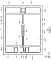
- Fig. 1 shows one example of an arrangement of each component on a front surface of a semiconductor device 100 according to Example 1.
- the semiconductor device 100 includes a semiconductor substrate 10, a gate pad 50, a current sensing pad 172, a temperature sensing unit 178, an anode pad 174 and a cathode pad 176 electrically connected to the temperature sensing unit 178, a bidirectional diode unit 210, and an output comparison diode unit 220.
- the semiconductor substrate 10 has an edge 102.
- a direction along one edge 102-1 of the semiconductor substrate 10 is considered to be an X axis direction, and a direction perpendicular to the X axis direction is considered to be a Y axis direction.
- the X axis is taken in a direction along the edge 102-1.
- a direction being perpendicular to the X axis direction and the Y axis direction, and forming a right-hand system with the X axis direction and the Y axis direction is referred to as a Z axis direction.
- the temperature sensing unit 178 of the present example is provided in a +Z axis direction of the semiconductor substrate 10.
- the semiconductor substrate 10 is formed of semiconductor material such as a silicon semiconductor or a compound semiconductor.
- a side of the semiconductor substrate 10 on which the temperature sensing unit 178 is provided is referred to as a front surface, and the opposite side is referred to as a back surface.
- a direction connecting the front surface and the back surface of the semiconductor substrate 10 is referred to as a depth direction.
- the semiconductor substrate 10 of the present example has a substantially rectangular shape on the front surface, the semiconductor substrate 10 may be in a different shape.
- the semiconductor substrate 10 has an active section 120 on the front surface.
- the active section 120 is a region in which main current flows in the depth direction between the front surface and the back surface of the semiconductor substrate 10 when the semiconductor device 100 is turned on.
- a gate conductor 44 in the active section 120 which will be described later, is connected to the gate pad 50 by a gate runner 48, which will also be described later.
- the active section 120 may be divided into an active section 120-1, an active section 120-2, an active section 120-3, an active section 120-4, an active section 120-5, and an active section 120-6 upon arrangement.
- the active section 120-1, the active section 120-3, and the active section 120-4 may be separated by a separation part 90 in the X axis direction.
- the active section 120-2, the active section 120-5, and the active section 120-6 may be separated by the separation part 90 in the X axis direction.
- the active section 120-1, the active section 120-3, and the active section 120-4 are arranged away from each other in the X axis direction in the present example, and electrically connected to each other by an emitter electrode 52, which will be described later.
- the active section 120-2, the active section 120-5, and the active section 120-6 are electrically connected to each other by the emitter electrode 52, which will be described later.
- the active section 120 may be provided with a transistor section 70 including a transistor element such as an IGBT (insulated gate bipolar transistor).
- the active section 120 may also be provided with a diode section 80 including a diode element such as a FWD (freewheeling diode).
- the transistor section 70 and the diode section 80 form an RC-IGBT (Reverse Conducting IGBT).
- the active section 120 may be a region in which at least one of the transistor section 70 and the diode section 80 is provided.
- a region in the active section 120 in which the transistor section 70 is arranged is marked with a character "I”
- a region in the active section 120 in which the diode section 80 is arranged is marked with a character "F”.
- the transistor section 70 and the diode section 80 may be alternately arranged in each region in the active section 120 along the X axis direction.
- the diode section 80 may be arranged on a negative X axis direction side in the active section 120-3.
- the semiconductor device 100 has a well region 130 of P+ type closer to the periphery of the front surface than the active section 120, and also has an edge termination structure closer to the periphery than the well region 130.
- the edge termination structure includes, for example, a guard ring that is annularly provided so as to surround the active section 120, or a field plate, or a combination thereof.
- the temperature sensing unit 178 may be arranged on a wide portion provided near the center of the front surface of the semiconductor substrate 10.
- the wide portion has no active section 120.
- the center of the semiconductor substrate 10 is easily heated by heat generated from switching devices which are formed in the active sections 120.
- Temperature of the transistor section 70 can be monitored by providing the temperature sensing unit 178 on the wide portion provided near the center. Thereby, overheating of the transistor section 70, which is caused by the transistor section 70 exceeding a bonding temperature Tj set as a range of a normal operation temperature, can be prevented.
- the temperature sensing unit 178 may be formed of a temperature sensing diode.
- the temperature sensing unit 178 is formed of a Shottky diode.
- the temperature sensing unit 178 may be formed of a polycrystal silicon PN junction diode provided above the semiconductor substrate 10 via an insulation film.
- An anode and a cathode of the temperature sensing diode are connected to a metal anode wiring 180 and a metal cathode wiring 182, respectively.
- the anode wiring 180 and the cathode wiring 182 contain metal such as aluminum.
- the cathode pad 176 is connected to the temperature sensing unit 178 via the cathode wiring 182.
- the anode pad 174 is connected to the temperature sensing unit 178 via the anode wiring 180.
- the cathode pad 176 and the anode pad 174 are electrodes containing metal such as aluminum.
- the current sensing pad 172 is electrically connected to a current sensing unit 110.
- the current sensing pad 172 is one example of the front surface electrode.
- the current sensing unit 110 has a structure similar to the structure of the transistor section 70 in the active section 120, and simulates operations of the transistor section 70. Current that flows into the current sensing unit 110 is in proportion to current that flows into the transistor section 70. Thereby, current flow of the transistor section 70 can be monitored.
- the current sensing unit 110 is different from the transistor section 70 in that the current sensing unit 110 has no emitter region 12, which will be described later. Thereby, the current sensing unit 110 does not operate as a transistor.
- the current sensing unit 110 is provided with a gate trench. The gate trench of the current sensing unit 110 is electrically connected to the gate runner 48.
- the bidirectional diode unit 210 is arranged between the anode pad 174 and the cathode pad 176 on the front surface of the semiconductor device 100.
- the bidirectional diode unit 210 includes a diode electrically connected in a serial bidirectional way between the anode pad 174 and the cathode pad 176.
- the bidirectional diode unit 210 prevents the temperature sensing unit 178 from being damaged by electro-static discharge (ESD).
- the output comparison diode unit 220 is provided between the anode pad 174 and the cathode pad 176.
- the output comparison diode unit 220 is electrically connected to the anode pad 174 and the cathode pad 176.
- the output comparison diode unit 220 includes an output comparison diode of which PN junction is connected in a direction being inverse parallel relative to a direction of PN junction of the temperature sensing diode included in the temperature sensing unit 178.
- the output comparison diode of the output comparison diode unit 220 may have the same design as a design of the diode of the temperature sensing unit 178, except that the direction of the PN junction.
- current is not applied to the output comparison diode unit 220.
- An output comparison operation which will be described later in Fig. 9A , is performed in each predetermined period.
- current is applied to the output comparison diode unit 220.
- timing of replacing the temperature sensing diode of the temperature sensing unit 178 can be recognized.
- a protective diode may be provided in parallel to the output comparison diode unit 220.
- a forward-direction of the protective diode may be the same as a forward-direction of the output comparison diode unit 220. In that case, the protective diode prevents the temperature sensing unit 178 from being applied with an overvoltage or receiving excessive current due to noise or the like during operation of the temperature sensing unit 178.
- Fig. 2 shows one example of an arrangement of the gate runner 48 on the front surface of the semiconductor device 100.
- the gate runner 48 is arranged at a position indicated by a dashed line on the front surface of the semiconductor substrate 10.
- the gate runner 48 is a wiring formed of polysilicon that is added with an impurity, or conductive material such as metal, which is covered by an insulation film such as polyimide.
- the gate runner 48 may be electrically connected to the gate pad 50.
- the gate runner 48 is also connected to the gate conductor 44, which will be described later, of the transistor section 70 arranged in the active section 120, and sets the gate conductor 44 to a gate potential.
- the gate conductor 44 corresponds to a gate electrode of the transistor section 70. Thereby, a transistor of the transistor section 70 is switched ON.
- the gate runner 48 may be arranged above the well region 130 in the vicinity of the active section 120.
- the gate runner 48 may be arranged in the wide portion provided near the center of the semiconductor substrate 10 and being between the active section 120-1 and the active section 120-2, so as to surround the temperature sensing unit 178.
- the gate pad 50 is electrically connected to an external control terminal.
- the gate pad 50 is formed of a conductor made of metal such as aluminum.
- the gate pad 50 may be externally connected by means of wire bonding.
- Fig. 3 is one example of an arrangement of the emitter electrode 52 provided on the front surface of the semiconductor device 100.
- the emitter electrode 52 is formed of a conductor made of metal such as aluminum.
- the emitter electrode 52 is set to an emitter potential being a predetermined reference potential.
- the emitter potential may be set to a ground potential. Similar to the current sensing pad 172, the emitter electrode 52 is another example of the front surface electrode.
- the emitter electrode 52 is arranged in a region indicated with diagonal lines.
- the emitter electrode 52 has a main metal portion 203 that entirely covers the active section 120.
- the emitter electrode 52 is provided in a region above the separation part 90 so as to electrically connect each of the active section 120-1, the active section 120-2, and the active section 120-3 which are separated from each other by the separation part 90 in the X axis direction.
- the active section 120-4, the active section 120-5, and the active section 120-6 are electrically connected to each other by the emitter electrode 52.
- the emitter electrode 52 has a connector 205 for connecting the main metal portion 203 and the bidirectional diode unit 210.
- the connector 205 may be provided integrally with the emitter electrode 52.
- the bidirectional diode unit 210 has one end electrically connected to the cathode pad 176, and the other end electrically connected to the emitter electrode 52 via the connector 205. Structure in the vicinity of the connector 205 will be described later.
- Fig. 4 shows one example of an enlarged view in the vicinity of the bidirectional diode unit 210 on the front surface of the semiconductor device 100.
- Fig. 4 is one example of an enlarged view of a region A in Fig. 3 .
- the bidirectional diode unit 210 includes two diode groups that are electrically connected in a serial bidirectional way such that cathodes in the diode groups face each other. Each of the two diode groups includes one or more diodes.
- the bidirectional diode unit 210 of the present example cathodes of each ten diodes that are electrically connected in series face each other.
- the bidirectional diode unit 210 of the present example includes Zener diodes connected in a bidirectional way.
- a Zener diode is formed by creating high doping concentration in a dopant diffusion region in a diode.
- the diode included in the bidirectional diode unit 210 is not limited to a Zener diode.
- a dopant in the diffusion region of the bidirectional diode unit 210 may be boron in a P type region, and arsenic in an N type region.
- the Zener diode has a large difference in band energy between a P type region and an N type region.
- Zener breakdown occurs due to electrons causing tunneling effect at a low voltage in a depletion layer.
- Zener breakdown phenomenon shows abrupt current change at a breakdown voltage with an occurrence of avalanche breakdown phenomenon, in which accelerated free electrons move across the depletion layer.
- the Zener diode shows low resistance when applied with a voltage of a certain value or more, which makes current drastically easy to flow into the Zener diode.
- an emitter potential is earthed, voltage from electro-static discharge is discharged to the ground potential.
- Zener diode has a polarity, by bidirectionally connecting Zener diodes in an anti-serial way, protection can be provided against overvoltage or excessive current caused by both of positive and negative voltage surges.
- the bidirectional diode unit 210 of the present example is arranged in a region between the anode pad 174 and the cathode pad 176.
- the temperature sensing unit 178 shows a larger resistance which causes deterioration to a temperature sensing characteristic of the temperature sensing unit 178. Since the bidirectional diode unit 210 of the present example is provided near the cathode pad 176, the bidirectional diode unit 210 can quickly perform operation in the vicinity of the cathode pad 176 in response to Zener breakdown. In this manner, the temperature sensing unit 178 is appropriately protected from electro-static discharge, thereby characteristics of the temperature sensing unit 178 can be maintained at a good level.
- the bidirectional diode unit 210 is arranged in a region between the anode pad 174 and the cathode pad 176, a space can be saved and utilized effectively when downsizing the semiconductor device 100. Further, since lengths of the anode wiring 180 and the cathode wiring 182 are kept short, a low self-inductance is maintained.
- the bidirectional diode unit 210 of the present example and the main metal portion 203 of the emitter electrode 52 are connected by the connector 205 that extends so as to cross over the gate runner 48.
- This arrangement of the connector 205 of the present example ensures a large area for the main metal portion 203 and the active section 120 to be provided.
- the output comparison diode unit 220 of the present example has three diodes which are connected in series. However, the number of diodes is not limited, provided that diodes are connected in series.
- the output comparison diode unit 220 may be arranged between the anode pad 174 and the cathode pad 176.
- a forward-direction of a PN junction in a diffusion region of the output comparison diode unit 220 is arranged so as to be opposite to a forward-direction of a PN junction of the temperature sensing diode of the temperature sensing unit 178, which is arranged parallel to the output comparison diode unit 220.
- the output comparison diode unit 220 may be a diode having the same structure as a structure of the temperature sensing unit 178, except that the output comparison diode unit 220 is connected in inverse parallel to the temperature sensing unit 178.
- Fig. 5 is one example of a top view of the semiconductor device 100. This diagram shows a front surface of the semiconductor device 100 on which the emitter electrode 52 is arranged, followed by the protective film 92 and the plated layer 230.
- the plated layer 230 is arranged in a region indicated with diagonal lines.
- the plated layer 230 includes metal such as nickel that is suitable for soldering.
- the plated layer 230 may be above the active section 120.
- a region C of the plated layer 230 is provided with a metal wiring layer, which is then electrically connected to a main terminal of the semiconductor device 100 by means of lead-free soldering or the like.
- the metal wiring layer is a lead frame including metal such as copper.
- the region C of the present example has a rectangular shape by way of example, and thus a shape of the region C is not limited to a rectangle.
- the protective film 92 is provided above the separation part 90 on the front surface of the semiconductor substrate 10.
- An extending portion 94 extends along the separation part 90 in a predetermined direction.
- the extending portion 94 of the present example extends in a Y axis direction.
- the extending portion 94 to extend may have a furrow-like (rib-like) shape.
- the protective film 92 includes, by way of example, an insulating material such as polyimide. Since each pad can be externally connected by means of wire bonding or the like, the protective film 92 may be provided on an upper surface of the current sensing pad 172, the anode pad 174, and the cathode pad 176.
- the bidirectional diode unit 210 may be arranged closer to a periphery of the front surface of the semiconductor substrate 10 than the extending portion 94.
- the furrow-like (rib-like) shape of the extending portion 94 can prevent solder from entering into the bidirectional diode unit 210 while soldering the plated layer 230.
- solder is asymmetrically formed, the semiconductor device 100 experiences stress concentration, a warpage caused by the stress concentration, peeling of an electrode, or the like. By preventing an overflowing of solder, the stress concentration caused by the solder can be prevented, as is peeling of an electrode. Thereby, reliability of the semiconductor device 100 improves.
- the protective film 92 is provided above the connector 205.
- the protective film 92 prevents solder from flowing into the connector 205 and the bidirectional diode unit 210 through the connector 205. Accordingly, the connector 205 having a narrower width than the main metal portion 203 can be prevented from experiencing stress concentration due to inflow of solder. Accordingly, reliability of the semiconductor device 100 improves.
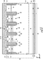
- Fig. 6 is one example of an XZ cross sectional view of the semiconductor device 100.
- the present example is one example of the cross section D-D' of Fig. 5 .
- the transistor section 70 has a plurality dummy trenches 30 and a plurality of gate trenches 40 on the front surface of the semiconductor substrate 10, and the diode section 80 has a plurality of dummy trenches 30 on the front surface of the semiconductor substrate 10.
- the semiconductor substrate 10 has a mesa portion 60 being a dopant diffusion region between each of the plurality of trenches. The mesa portion 60 is connected to an emitter electrode via a contact hole 54.
- the dummy trench 30 has a dummy insulating film 32 and a dummy conductor 34.
- the dummy conductor 34 is electrically connected to the emitter electrode 52 via a contact hole, which will be described later, and set to the emitter potential.
- the gate trench 40 includes the gate conductor 44 configured by a conductor such as metal, and a gate insulating film 42 provided between the gate conductor 44 and the active section 120.
- the gate conductor 44 is insulated from the emitter electrode 52 by an interlayer dielectric film 38.
- the gate conductor 44 is electrically connected to the gate pad 50 by the gate runner 48, and set to the gate potential.
- the gate conductor 44 corresponds to the gate electrode of the transistor section 70.
- the gate potential may be a higher potential than the emitter potential.
- the transistor section 70 has an emitter region 12 of a first conductivity type, a base region 14 of a second conductivity type, a drift region 18 of the first conductivity type provided under the base region 14, and a collector region 22 of the second conductivity type in this order from the front surface of the semiconductor substrate 10.
- the emitter region 12 may only cover regions near the dummy trench 30 and the gate trench 40 instead of covering the entire mesa portion 60 on the front surface of the semiconductor substrate 10.
- a region in which the mesa portion 60 is not covered by the emitter region 12 may have the base region 14 exposed on the front surface.
- the transistor section 70 of the present example has an accumulation region 16 of a first conductivity type that is provided between the base region 14 and the drift region 18.
- carrier IE injection Enhancement
- the accumulation region 16 may be omitted.
- an electrode type of the emitter region 12 is N+ type. That is, in the present example, a first conductivity type is N type and a second conductivity type is P type. However, the first conductivity type may be P type and the second conductivity type may be N type instead. In this case, conductivity types of substrates, layers, regions, or the like in each embodiment example would be of inverse polarity.
- the base region 14 of the present example has a P- type polarity.
- the gate conductor 44 When the gate conductor 44 is set to the gate potential, electrons are withdrawn in the base region 14 toward the gate trench 40.
- An N type channel is then formed in a region in which the base region 14 is in direct contact with the gate trench 40, and thus drives as a transistor.
- a P- type base region 14 is provided on the upper surface 21 of the semiconductor substrate 10.
- the diode section 80 of the present example has no accumulation region 16.
- the diode section 80 may have an accumulation region 16.
- An N- type drift region 18 is provided under the accumulation region 16 of the transistor section 70, and under the base region 14 of the diode section 80.
- An N type buffer region 20 is provided under the drift region 18 of both of the transistor section 70 and the diode section 80.
- the buffer region 20 may serve as a field stop layer for preventing a depletion layer expanding from the lower surface of the base region 14 from reaching a P+ type collector region 22 and an N+ type cathode region 82.
- the P+ type collector region 22 is provided under the buffer region 20.
- the N+ type of cathode region 82 is provided under the buffer region 20.
- a surface under the collector region 22 and the cathode region 82 corresponds to a lower surface 23 of the semiconductor substrate 10.
- the lower surface 23 of the semiconductor substrate 10 is provided with a collector electrode 24.
- the collector electrode 24 is formed of a conductive material such as metal.
- Fig. 7 is one example of a cross sectional view in the vicinity of a connector 205 and the bidirectional diode unit 210 of the semiconductor device 100.
- the present example is one example of the cross section B-B' of Fig. 4 and the E-E' cross section of Fig. 5 .
- the transistor section 70 is provided in the active section 120 near the well region 130.
- the diode section 80 may be provided in this region instead.
- the emitter electrode 52 is provided above the active section 120, and the plated layer 230 is provided above the emitter electrode 52.
- the protective film 92 is provided above the connector 205 and the bidirectional diode unit 210.
- a diffusion region under the well region 130 may be of the same structure as that of the transistor section 70.
- the emitter electrode 52 has the connector 205.
- the connector 205 of the present example crosses over the gate runner 48.
- An end of the connector 205 is connected to a wiring 216 between diffusion regions which is connected to an anode of the bidirectional diode unit 210.
- the bidirectional diode unit 210 has wirings 216 between diffusion regions which are connected to cathodes connected in an anti-serial way so as to face each other. Diffusion regions of the gate runner 48 and the bidirectional diode unit 210 may be insulated by the interlayer dielectric film 38.
- Fig. 8 is one example of an equivalent circuit diagram of the semiconductor device 100.
- the semiconductor device 100 of the present example has such structure that a transistor section 70 of which collector is connected to a collector of the current sensing unit 110 that has the same gate potential as the transistor section 70.
- the transistor section 70 and the diode section 80 of the present example has a RC-IGBT.
- the bidirectional diode unit 210 of the present example has one end connected to an emitter of the transistor section 70, and the other end connected to a cathode of the temperature sensing unit 178.
- the electric connection of the bidirectional diode unit 210 of the present example has no influence on a readout voltage value of the temperature sensing unit 178.
- a circuit symbol of the bidirectional diode unit 210 is illustrated as a Zener diode.
- a diode of the bidirectional diode unit 210 is not limited to the Zener diode.
- An output comparison diode unit 220 is arranged in a manner that a diode included in the protective diode unit 220 is electrically connected in inverse parallel to the temperature sensing unit 178. Both ends of the temperature sensing unit 178 may be connected to a circuit having functions of detecting current and voltage of the temperature sensing unit 178, and calculating a temperature.
- a wiring between the bidirectional diode unit 210 and the temperature sensing unit 178 shows resistance and self-reactance when implemented in the semiconductor device 100.
- a distance between the bidirectional diode unit 210 and the cathode of the temperature sensing unit 178 is long, a time difference may emerge from when electro-static discharge occurs to when Zener operation is performed by the bidirectional diode unit 210.
- the semiconductor device 100 of the present example has the bidirectional diode unit 210 arranged between the anode pad 174 and the cathode pad 176, and thereby ensures the Zener operation to be performed quickly. Further, even when a chip of the semiconductor device 100 is downsized upon providing a circuit element on the chip, providing the bidirectional diode unit 210 at this position reduces influence on other elements in a circuit layout. By arranging the bidirectional diode unit 210 and the output comparison diode unit 220 in this manner of the present example, a protection element of the temperature sensing unit 178 can be arranged away from an active section 120 through which a large current flow. In this manner, ESD withstand capability of the semiconductor device 100 can be improved while circuit reliability is maintained.
- Fig. 9A is a circuit diagram of a part in which the temperature sensing unit 178 and the output comparison diode unit 220 are arranged in parallel.
- One example of output comparison operation of the output comparison diode unit 220 of the present example will be described below.
- Direction of input current is switched in order to apply current of a predetermined level in a forward-direction of the output comparison diode of the output comparison diode unit 220.
- This current may be the same level as the current applied to the temperature sensing unit 178, or may also be a different level.
- an output voltage of the output comparison diode is measured.
- a voltage difference value between the output voltage of the temperature sensing diode and the output voltage of the output comparison diode is measured. Thereby, calibration is performed on an initial value ⁇ V int of the voltage difference value.
- ⁇ V int is set to zero.
- the temperature sensing unit 178 detects temperature on the semiconductor substrate 10.
- the temperature sensing unit 178 is driven with continuous supply of current of a predetermined certain level.
- the temperature sensing unit 178 is formed of a polycrystal silicon PN junction diode and used for a long period of time, a recombination process takes place in the polycrystal due to current being applied. Thereby, more crystal defects are produced and an amount of crystal defects is increased. Production speed of the crystal defect is in proportion to a level of current to be applied for driving the temperature sensing unit 178.
- the temperature sensing unit 178 when the temperature sensing unit 178 is continuously driven, more crystal defects occur in the temperature sensing unit 178, and an output voltage Vf decreases.
- a rate of ⁇ Vf which is obtained from a variation amount of the output voltage Vf of the temperature sensing unit 178 to a predetermined input current, exceeds a predetermined threshold value, the temperature sensing unit 178 can be specified as having reached the end of its service life.
- the threshold value is set to 2%.
- direction of input current is switched in order to apply current of a predetermined level in the forward-direction of the output comparison diode of the output comparison diode unit 220.
- an output voltage of the output comparison diode unit 220 is measured.
- a voltage difference value ⁇ V between the output voltage of the temperature sensing diode and the output voltage of the output comparison diode is measured. Deducting ⁇ V int from ⁇ V can lead to a variation amount ⁇ Vf of an output voltage that changes with lapse of time. A variation rate of the output voltage Vf is obtained from a ratio of ⁇ Vf to Vf int , that is, ⁇ Vf/Vf int .
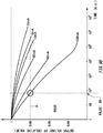
- Fig. 9B shows one example of aging deterioration of a polycrystal silicon PN junction diode.
- the temperature sensing unit 178 is a polycrystal silicon PN junction diode, being driven with current leads to an increase in crystal defect.
- the graph uses a logarithmic scale on the horizontal axis.
- Each scale on the horizontal axis represents time that increases exponentially.
- the vertical axis represents a relative value of an output voltage Vf of the temperature sensing diode.
- an initial value of the output voltage Vf is scaled to one.
- the temperature sensing diode when variation in the output voltage of the output voltage Vf of the temperature sensing diode is 2% or more, the temperature sensing diode is specified as having reached the end of its service life. For example, when a driving current is 100 mA, the output voltage Vf decreases by 2% at a point of time represented with a value 80.
- a value of current to be applied for driving the temperature sensing unit 178 is in proportion to production speed of crystal defect. Therefore, a negative correlation exists between an exponentiation value of a level of driving current of the temperature sensing diode and service life of the temperature sensing diode.
- Service life of the temperature sensing unit 178 can be extended by reducing the driving current.
- reducing the driving current increases influence of noise from the bidirectional diode unit 210 to such an extent that the influence can not be ignored.
- measurement sensitivity can be ensured for the temperature sensing diode even when there is the influence of noise.
- an output comparison diode unit 220 for detecting service life of the temperature sensing diode a user can judge timing of replacing the temperature sensing diode with an actual product. This allows the user to replace the temperature sensing diode according to the service life even when the measurement sensitivity is increased for the temperature sensing unit 178. Hence, there is no need in choosing an oversized product for long service life, and instead a compact product can be used as the temperature sensing diode. In this manner, a further die shrink can be achieved on the semiconductor device 100, and flexibility is increased for designing the measurement sensitivity of the temperature sensing diode.
- Fig. 9C shows one example of a deterioration detection circuit 300 provided external to the semiconductor device 100.
- the deterioration detection circuit 300 includes a detector 302-a, a detector 302-b, a detector 302-c, and a detector 302-d, a latch circuit 304, a switching unit 310, and an overheating protection circuit 320.
- One end of a terminal of the deterioration detection circuit 300 is connected to an input voltage VDD, and a ground voltage GND
- the deterioration detection circuit 300 of the present example includes four detectors 302, a switching number between the detectors 302 and the switching unit 310 is not limited to four.
- the semiconductor device 100 and the deterioration detection circuit 300 may be integrated in one system.
- the switching unit 310 has a plurality of switches.
- the switching unit 310 switches the plurality of switches in order to conduct current to a cathode and an anode of the temperature sensing unit 178 of the semiconductor device 100, or to switch the current to be conducted between positive current and negative current through any of the detector 302-a, the detector 302-b, the detector 302-c, and the detector 302-d.
- the switching unit 310 conducts current in the forward-direction of the temperature sensing unit 178 via the detector 302-a.
- the detector 302-a in the overheating protection circuit 320 is activated to measure an output voltage Vf of the temperature sensing unit 178. Through the measurement of the output voltage Vf, whether or not the semiconductor device 100 is overheated is detected.
- the detector 302-b and the detector 302-c are used in output comparison operation.
- the detector 302-b detects an output voltage Vf upon applying current in the forward-direction of the temperature sensing unit 178.
- the detector 302-c detects an output voltage upon applying current in the forward-direction of the output comparison diode unit 220.
- the latch circuit 304 is for latching the output voltage Vf and the output voltage of the output comparison diode unit 220.
- the latch circuit 304 delivers each voltage to the detector 302-d.
- the detector 302-d is for detecting the voltage difference value ⁇ Vf.
- the detector 302-d compares a voltage difference value and a predetermined threshold value, and transmits a notice of recommendation for replacing the temperature sensing diode when the voltage difference value is larger than the threshold value.
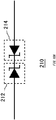
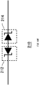
- Fig. 10A shows one example of the bidirectional diode unit 210.
- the bidirectional diode unit 210 includes a first diode portion 212 and a second diode portion 214 which are electrically connected in an anti-serial way.
- Each of the first diode portion 212 and the second diode portion 214 of the present example has a diode. This diode is illustrated with a circuit symbol of a Zener diode in the circuit diagram.
- each of the first diode portion 212 and the second diode portion 214 has one Zener diode.
- a cathode of the first diode portion 212 and a cathode of the second diode portion 214 face each other.
- Fig. 10B shows another example of the bidirectional diode unit 210.
- an anode of a first diode portion 212 and an anode of a second diode portion 214 face each other.
- Both of the bidirectional diode units 210 shown in Fig. 10A and Fig. 10B can provide protection against electro-static discharge.
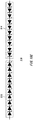
- Fig. 10C shows yet another example of the bidirectional diode unit 210.
- This bidirectional diode unit 210 has the same configuration as that of the bidirectional diode unit 210 shown in Fig. 4 .
- Each of a first diode portion 212 and a second diode portion 214 has ten Zener diodes. Diodes of the first diode portion 212 are electrically connected in series.
- Fig. 10D shows yet another example of the bidirectional diode unit 210.
- each of a first diode portion 212 and a second diode portion 214 has ten Zener diodes.
- Each of the first diode portion 212 and the second diode portion 214 has two lines of five diodes, which are connected in parallel.
- each of a first diode portion 212 and a second diode portion 214 may include a plurality of diodes connected in parallel.
- the first diode portion 212 and the second diode portion 214 may have three or more parallel numbers. Further, more than one diode may be included in each of wirings connected in parallel.
- a value of current that flows in the bidirectional diode unit 210 of Fig. 10D is approximately twice as much as a value of current that flows in the bidirectional diode unit 210 of Fig. 10C .
- electro-static discharge occurs, current flows in the bidirectional diode unit 210 of Fig. 10D instantaneously faster and easier than in the bidirectional diode unit 210 of Fig. 10C .
- the bidirectional diode unit 210 of Fig. 10D has ESD withstand capability higher than that of the bidirectional diode unit 210 of Fig. 10C .
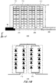
- Fig. 11A is one example of the P type region and the N type region provided in the bidirectional diode unit 210.
- the bidirectional diode unit 210 of the present example has the same structure as that of the example of the bidirectional diode unit 210 shown in Fig. 4 .
- the example of the bidirectional diode unit 210 of Fig. 4 is shown together with an equivalent circuit diagram.
- Each of a first diode portion 212 and a second diode portion 214 of the bidirectional diode unit 210 of the present example includes a set of ten diodes which are provided in series.
- a cathode of the first diode portion 212 faces a cathode of the second diode portion 214.
- the wiring 216 between diffusion regions electrically connects the P type region and the N type region over the interlayer dielectric film 38.
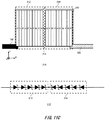
- Fig. 11B is another example of the P type region and the N type region provided in the bidirectional diode. This example has the same structure as that of the example of the circuit according to the bidirectional diode unit 210 shown in Fig. 10D .
- the parallel number of diodes in the bidirectional diode unit 210 and the number of diodes in each parallel wiring can be adjusted.
- a parallel number of wirings of a first diode portion 212 is two.
- each of the parallel wirings has five diodes.
- a second diode portion 214 has the same structure as that of the first diode portion 212.
- Fig. 11C is yet another example of the P type region and the N type region provided in the bidirectional diode.
- each of a first diode portion 212 and a second diode portion 214 has five Zener diodes.
- a diode included in the bidirectional diode unit 210 of the present example has a long width in a Y axis direction. Therefore, area of a PN junction region is larger than that of the bidirectional diode unit 210 of Fig. 11A . Accordingly, more current flows in the bidirectional diode unit 210 of the present example than in the bidirectional diode unit 210 according to Fig. 11A . Therefore, the bidirectional diode unit 210 has ESD withstand capability larger than that of the bidirectional diode unit 210 according to Fig. 11A .
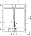
- Fig. 12 shows one example of an arrangement of each component on a front surface of a semiconductor device 100 according to Example 2. Difference between the present example and Example 1 will be particularly described below.
- a bidirectional diode unit 210 is electrically connected to a current sensing pad 172 and a cathode pad 176 by a sensing pad wiring 232.
- a front surface electrode to be connected to the bidirectional diode unit 210 corresponds to the current sensing pad 172. That is, the front surface electrode may include the current sensing pad 172 being connected to a current sensing unit 110.
- the bidirectional diode unit 210 of the present example is arranged between an anode pad 174 and the cathode pad 176, the temperature sensing unit 178 is appropriately protected from electro-static discharge, thereby characteristics of the temperature sensing unit 178 can be maintained at a good level. Further, even when a chip of the semiconductor device 100 is downsized, ESD withstand capability of the semiconductor device 100 can be improved while maintaining reliability of a circuit.
- the bidirectional diode unit 210 can provide not only the temperature sensing unit 178 but also the current sensing unit 110 with protection against electro-static discharge.
- Fig. 13 shows an equivalent circuit diagram of the semiconductor device 100 according to Example 2.
- the bidirectional diode unit 210 has one end electrically connected to an emitter electrode of the current sensing unit 110, and the other end connected to a cathode of the temperature sensing unit 178.
- Fig. 14 shows one example of an arrangement of each component on a front surface of a semiconductor device 100 according to Example 3.
- a bidirectional diode unit 210 is arranged next to a temperature sensing unit 178 near the center of the semiconductor device 100.
- the semiconductor device 100 of the present example has the same equivalent circuit as that of Example 1 shown in Fig. 8 .
- the semiconductor device 100 of the present example has the same equivalent circuit as that of Example 1. Difference between the present example and Example 1 will be particularly described with reference to the following enlarged view.
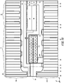
- Fig. 15 is one example of an enlarged view of near the center of the front surface of the semiconductor device 100 according to Example 3.
- the present example is one example of an enlarged view of a region F shown in Fig. 14 .
- the bidirectional diode unit 210 of the present example includes diodes which are electrically connected in a serial bidirectional way between a cathode wiring 182 and an emitter electrode 52 being a front surface electrode.
- the bidirectional diode unit 210 of the present example is arranged on a front surface of the semiconductor device 100, and between the cathode wiring 182 and the emitter electrode 52 in a Y axis direction.
- the bidirectional diode unit 210 is arranged such that the cathode wiring 182 is between the bidirectional diode unit 210 and the temperature sensing unit 178 in an X axis direction.
- the cathode wiring 182 is electrically connected to an N type region on a cathode side of temperature sensing diodes of the temperature sensing unit 178, which are arranged in series.
- An anode wiring 180 is electrically connected to a P type region on an anode side of the temperature sensing diodes.
- the cathode wiring 182 and the anode wiring 180 may be curved and extend in a U-shape. Active regions of the temperature sensing unit 178 may be connected by a temperature-sensing wire 183.
- the cathode wiring 182 of the present example is also electrically connected to one end of the bidirectional diode unit 210. Another end of the bidirectional diode unit 210 of the present example is electrically connected to a connector 205 extending in a Y axis direction from a transistor section 70 of an active section 120-2.
- a gate runner 48 is arranged as illustrated by a dashed line.
- the gate runner 48 may be connected to a gate conductor 44 of a gate trench 40.
- a dummy conductor 34 of a dummy trench 30 is connected to the emitter electrode 52 via a contact hole.
- a plated layer 230 is provided over an active section 120, and a protective film 92 is provided in a region without the active section 120. In this manner, wirings can be provided without being connected by plating.
- the bidirectional diode unit 210 is arranged near the temperature sensing unit 178.
- An interlayer dielectric film 38 between an active region of the temperature sensing diode and the active section 120 is easily influenced by electro-static discharge.
- This arrangement of the present example permits the bidirectional diode unit 210 to quickly perform a Zener operation in order to appropriately provide a part of the temperature sensing unit 178, which is subjected to be easily influenced by electro-static discharge, with protection against the electro-static discharge.
- the transistor section 70 and a diode section 80 in a rectangular shape in the active section 120 reduces man-hours and cost in manufacturing.
- the transistor section 70 and the diode section 80 of a rectangular shape are adopted, and when creating a wide portion for disposing the temperature sensing unit 178 at the center, space is likely to be formed in the vicinity of the temperature sensing unit 178.
- this space in the vicinity of the temperature sensing unit 178 can be effectively utilized. Therefore, in the present example, the semiconductor device 100 with excellent reliability, which supports downsizing of a chip of the semiconductor device 100, can be provided with protection against electro-static.
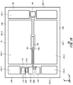
- Fig. 16 shows one example of an arrangement of each component on a front surface of the semiconductor device 100 according to Example 4.
- the semiconductor device 100 of the present example has the same equivalent circuit as that of Example 2 shown in Fig. 13 . Difference between the present example and Example 2 will be particularly described below.
- an active region of a temperature sensing unit 178 has an inverse polarity relative to that of Example 4. Therefore, a cathode pad 176 and an anode pad 174 are arranged in reverse order relative to that of Example 4. Note that, exchanging the positions of the cathode pad 176 and the anode pad 174 may be performed by changing positions of an anode wiring 180 and a cathode wiring 182.
- a bidirectional diode unit 210 is arranged between a current sensing pad 172 and the cathode pad 176 on a front surface of a semiconductor substrate 10. Similar to Example 2, the bidirectional diode unit 210 is electrically connected to the current sensing pad 172 and the cathode pad 176. This may be achieved by means of a connector 205 extending from a front surface electrode of the current sensing pad 172.
- An upper surface of the connector 205 is provided with a protective film 92. In this manner, the connector 205 and the bidirectional diode unit 210 are less likely to receive solder from a plated layer. Thereby, stress concentration can be prevented from occurring on the connector 205.
Landscapes
- Engineering & Computer Science (AREA)
- Microelectronics & Electronic Packaging (AREA)
- Physics & Mathematics (AREA)
- General Physics & Mathematics (AREA)
- Semiconductor Integrated Circuits (AREA)
- Metal-Oxide And Bipolar Metal-Oxide Semiconductor Integrated Circuits (AREA)
Abstract
Description
- The present invention relates to a semiconductor device.
- Conventionally, a semiconductor device having a protective diode provided between a MOSFET (Metal Oxide Semiconductor Field Effective Transistor) or the like and a temperature detecting diode has been known (for example, refer to Patent Document 1).
- Patent Document 1:
Japanese Patent Application Publication No. 2006-203446 - Providing a temperature detecting diode with protection against electro-static discharge.
- In order to achieve the above-mentioned task, a first aspect of the present invention provides a semiconductor device including: a semiconductor substrate; a temperature sensing unit provided on a front surface of the semiconductor substrate; an anode pad and a cathode pad electrically connected with the temperature sensing unit; a front surface electrode being set to a predetermined reference potential; and a bidirectional diode unit electrically connected in a serial bidirectional way between the cathode pad and the front surface electrode. An output comparison diode unit is arranged between the anode pad and the cathode pad. The temperature sensing unit includes a temperature sensing diode. The output comparison diode unit includes a diode that is connected in inverse parallel with the temperature sensing diode.
- The bidirectional diode unit may be arranged between the anode pad and the cathode pad on the front surface.
- The bidirectional diode unit may include a Zener diode connected in a bidirectional way.
- The front surface electrode may have a main metal portion provided on the front surface, and a connector for connecting the main metal portion and the bidirectional diode unit.
- The semiconductor device may include a transistor section, and a gate runner that is provided on the front surface of the semiconductor substrate and electrically connected to a gate electrode of the transistor section. The connector may cross over the gate runner.
- The semiconductor device may also include a current sensing unit. The front surface electrode may include a current sensing pad electrically connected to the current sensing unit.
- The semiconductor device may include a protective film that is provided above the connector.
- The protective film may include polyimide.
- The protective film may have an extending portion extending in a predetermined direction on the front surface of the semiconductor substrate. The bidirectional diode unit may be arranged closer to a periphery of the front surface of the semiconductor substrate than the extending portion.
- The bidirectional diode unit may have a first diode portion, and a second diode portion connected in an anti-serial way to the first diode portion. Each of the first diode portion and the second diode portion may include a plurality of diodes connected in parallel.
- A second aspect of the present invention provides a system including: a semiconductor device; and a deterioration detection circuit having a switching unit and a detector, the switching unit is for being electrically connected to the temperature sensing unit and the output comparison diode unit of the semiconductor device, and applying current in a forward-direction of each of the temperature sensing unit and the output comparison diode unit by switching a direction of current to be applied, and the detector is for measuring a voltage difference value between an output voltage of when current is input in a forward-direction of the temperature sensing unit and an output voltage of when current is input in a forward-direction of the output comparison diode unit.
- The detector may compare a voltage difference value and a predetermined threshold value, and transmit a notice of recommendation for replacing the temperature sensing diode when the voltage difference value is larger than the threshold value.
- A third aspect of the present invention provides a semiconductor device including: a semiconductor substrate; a temperature sensing unit provided on a front surface of the semiconductor substrate; an anode wiring and a cathode wiring electrically connected to the temperature sensing unit; a front surface electrode being set to a predetermined reference potential; and a bidirectional diode unit electrically connected in a serial bidirectional way between the cathode wiring and the front surface electrode. The bidirectional diode unit may be arranged between the cathode wiring and the front surface electrode on the front surface.
- The bidirectional diode unit may be arranged such that the cathode wiring is between the bidirectional diode unit and the temperature sensing unit.
- A fourth aspect of the present invention provides a semiconductor device including: a semiconductor substrate; a temperature sensing unit provided on a front surface of the semiconductor substrate; an anode pad and a cathode pad electrically connected to the temperature sensing unit; a current sensing unit; a current sensing pad being set to a predetermined reference potential and electrically connected to the current sensing unit; and a bidirectional diode unit electrically connected in a serial bidirectional way between the cathode pad and the current sensing pad. The bidirectional diode unit may be arranged between the current sensing pad and the cathode pad on the front surface.
- The summary clause does not necessarily describe all necessary features of the embodiments of the present invention. The present invention may also be a sub-combination of the features described above.
-
-
Fig. 1 shows one example of an arrangement of each component on a front surface of asemiconductor device 100 according to Example 1. -
Fig. 2 shows one example of an arrangement of agate runner 48 on the front surface of thesemiconductor device 100. -
Fig. 3 is one example of an arrangement of anemitter electrode 52 provided on the front surface of thesemiconductor device 100. -
Fig. 4 shows one example of an enlarged view in the vicinity of abidirectional diode unit 210 on the front surface of thesemiconductor device 100. -
Fig. 5 is one example of a top view of thesemiconductor device 100. -
Fig. 6 is one example of an XZ cross sectional view of thesemiconductor device 100. -
Fig. 7 is one example of a cross sectional view in the vicinity of aconnector 205 and thebidirectional diode unit 210 of thesemiconductor device 100. -
Fig. 8 is one example of an equivalent circuit diagram of thesemiconductor device 100. -
Fig. 9A is a circuit diagram of a part in which thetemperature sensing unit 178 and the outputcomparison diode unit 220 are arranged in parallel. -
Fig. 9B shows one example of aging deterioration of a polycrystal silicon PN junction diode. -
Fig. 9C shows one example of adeterioration detection circuit 300 provided external to thesemiconductor device 100. -
Fig. 10A shows one example of thebidirectional diode unit 210. -
Fig. 10B shows another example of thebidirectional diode unit 210. -
Fig. 10C shows yet another example of thebidirectional diode unit 210. -
Fig. 10D shows yet another example of thebidirectional diode unit 210. -
Fig. 11A is one example of a P type region and an N type region provided in thebidirectional diode unit 210. -
Fig. 11B is another example of the P type region and the N type region provided in the bidirectional diode. -
Fig. 11C is yet another example of the P type region and the N type region provided in the bidirectional diode. -
Fig. 12 shows one example of an arrangement of each component on a front surface of asemiconductor device 100 according to Example 2. -
Fig. 13 shows an equivalent circuit diagram of thesemiconductor device 100 according to Example 2. -
Fig. 14 shows one example of an arrangement of each component on a front surface of asemiconductor device 100 according to Example 3. -
Fig. 15 is one example of an enlarged view in the vicinity of the center of the front surface of thesemiconductor device 100 according to Example 3. -
Fig. 16 shows one example of an arrangement of each component on a front surface of thesemiconductor device 100 according to Example 4. - Hereinafter, the present invention will be described with embodiments of the invention. However, the following embodiments have no intention of limiting the claimed invention. In addition, some combinations of features described in the embodiments may be unnecessary for solving means of the invention.
- Herein, one side of a semiconductor substrate in a direction parallel to a depth direction of the semiconductor substrate is referred to as "front" or "upper", and the opposite side is referred to as "back" or "lower". One of two main surfaces of a substrate, a layer or another member is referred to as an upper surface, and the other is referred to as a lower surface. The direction indicated by "front", "upper", "back", or "lower" is not limited to the gravitational direction or direction of implementing the semiconductor device.
- As used herein, technical matters may be described by use of orthogonal coordinate axes of an X axis, a Y axis and a Z axis. The orthogonal coordinate axes are merely used for specifying relative positions between components, and thus not used for limiting the components in a specific direction. For example, the Z axis shall not exclusively indicate a height direction relative to the ground. Note that, a +Z axis direction and a -Z axis direction are directions opposite to each other. When the Z axis direction is described without a positive or a negative sign, the Z axis direction indicates a direction parallel to the +Z axis and the -Z axis. Also, as used herein, a top plan view may be a view seen from the +Z axis direction.
- One mentioned herein as "the same" or "equal" may include one with error derived from a variation in manufacturing or the like. This error is the one within a range of 10%, for example.
- As used herein, a conductivity type of a doping region doped with an impurity is described as P type or N type. However, the conductivity type of each doping region may also be of inverse polarity. Also, as used herein, P+ type or N+ type has doping concentration higher than that of P type or N type, respectively, and P- type or N- type has doping concentration lower than that of P type or N type, respectively.
- As used herein, doping concentration refers to concentration of impurities activated as donors or acceptors. As used herein, the concentration difference between donors and acceptors may be concentration of the one with higher concentration between the donors and the acceptors. The concentration difference can be measured by the capacitance-voltage profiling (CV profiling). Further, carrier concentration measured by the spreading resistance (SR) profiling may be considered as concentration of donors or acceptors. Furthermore, when concentration distribution of donors or acceptors has a peak in a region, a value of the peak may be set as concentration of the donors or the acceptors in this region. In a region where donors or acceptors are present, when concentration of the donors or the acceptors is substantially uniform or the like, an average value of donor concentration or acceptor concentration in this region may be set as donor concentration or acceptor concentration.
-
Fig. 1 shows one example of an arrangement of each component on a front surface of asemiconductor device 100 according to Example 1. Thesemiconductor device 100 includes asemiconductor substrate 10, agate pad 50, acurrent sensing pad 172, atemperature sensing unit 178, ananode pad 174 and acathode pad 176 electrically connected to thetemperature sensing unit 178, abidirectional diode unit 210, and an outputcomparison diode unit 220. - The
semiconductor substrate 10 has anedge 102. As used herein, in a top plan view ofFig. 1 , a direction along one edge 102-1 of thesemiconductor substrate 10 is considered to be an X axis direction, and a direction perpendicular to the X axis direction is considered to be a Y axis direction. In the present example, the X axis is taken in a direction along the edge 102-1. A direction being perpendicular to the X axis direction and the Y axis direction, and forming a right-hand system with the X axis direction and the Y axis direction is referred to as a Z axis direction. Thetemperature sensing unit 178 of the present example is provided in a +Z axis direction of thesemiconductor substrate 10. - The
semiconductor substrate 10 is formed of semiconductor material such as a silicon semiconductor or a compound semiconductor. A side of thesemiconductor substrate 10 on which thetemperature sensing unit 178 is provided is referred to as a front surface, and the opposite side is referred to as a back surface. As used herein, a direction connecting the front surface and the back surface of thesemiconductor substrate 10 is referred to as a depth direction. Although thesemiconductor substrate 10 of the present example has a substantially rectangular shape on the front surface, thesemiconductor substrate 10 may be in a different shape. - The
semiconductor substrate 10 has anactive section 120 on the front surface. Theactive section 120 is a region in which main current flows in the depth direction between the front surface and the back surface of thesemiconductor substrate 10 when thesemiconductor device 100 is turned on. Agate conductor 44 in theactive section 120, which will be described later, is connected to thegate pad 50 by agate runner 48, which will also be described later. - The
active section 120 may be divided into an active section 120-1, an active section 120-2, an active section 120-3, an active section 120-4, an active section 120-5, and an active section 120-6 upon arrangement. Specifically, the active section 120-1, the active section 120-3, and the active section 120-4 may be separated by aseparation part 90 in the X axis direction. Similarly, the active section 120-2, the active section 120-5, and the active section 120-6 may be separated by theseparation part 90 in the X axis direction. The active section 120-1, the active section 120-3, and the active section 120-4 are arranged away from each other in the X axis direction in the present example, and electrically connected to each other by anemitter electrode 52, which will be described later. Similarly, the active section 120-2, the active section 120-5, and the active section 120-6 are electrically connected to each other by theemitter electrode 52, which will be described later. - The
active section 120 may be provided with atransistor section 70 including a transistor element such as an IGBT (insulated gate bipolar transistor). Theactive section 120 may also be provided with adiode section 80 including a diode element such as a FWD (freewheeling diode). When theactive section 120 is provided with the IGBT and the FWD, thetransistor section 70 and thediode section 80 form an RC-IGBT (Reverse Conducting IGBT). Theactive section 120 may be a region in which at least one of thetransistor section 70 and thediode section 80 is provided. - In the present example, a region in the
active section 120 in which thetransistor section 70 is arranged is marked with a character "I", and a region in theactive section 120 in which thediode section 80 is arranged is marked with a character "F". Thetransistor section 70 and thediode section 80 may be alternately arranged in each region in theactive section 120 along the X axis direction. - Note that, this is an example of an arrangement of the
transistor section 70 and thediode section 80 of the present example, and thus different arrangement may also be adopted. For example, thediode section 80 may be arranged on a negative X axis direction side in the active section 120-3. - The
semiconductor device 100 has awell region 130 of P+ type closer to the periphery of the front surface than theactive section 120, and also has an edge termination structure closer to the periphery than thewell region 130. The edge termination structure includes, for example, a guard ring that is annularly provided so as to surround theactive section 120, or a field plate, or a combination thereof. - The
temperature sensing unit 178 may be arranged on a wide portion provided near the center of the front surface of thesemiconductor substrate 10. The wide portion has noactive section 120. When theactive sections 120 of thesemiconductor substrate 10 are integrated, the center of thesemiconductor substrate 10 is easily heated by heat generated from switching devices which are formed in theactive sections 120. Temperature of thetransistor section 70 can be monitored by providing thetemperature sensing unit 178 on the wide portion provided near the center. Thereby, overheating of thetransistor section 70, which is caused by thetransistor section 70 exceeding a bonding temperature Tj set as a range of a normal operation temperature, can be prevented. - The
temperature sensing unit 178 may be formed of a temperature sensing diode. By way of example, thetemperature sensing unit 178 is formed of a Shottky diode. Alternatively, thetemperature sensing unit 178 may be formed of a polycrystal silicon PN junction diode provided above thesemiconductor substrate 10 via an insulation film. - An anode and a cathode of the temperature sensing diode are connected to a
metal anode wiring 180 and ametal cathode wiring 182, respectively. Theanode wiring 180 and thecathode wiring 182 contain metal such as aluminum. - The
cathode pad 176 is connected to thetemperature sensing unit 178 via thecathode wiring 182. Theanode pad 174 is connected to thetemperature sensing unit 178 via theanode wiring 180. Thecathode pad 176 and theanode pad 174 are electrodes containing metal such as aluminum. - The
current sensing pad 172 is electrically connected to acurrent sensing unit 110. Thecurrent sensing pad 172 is one example of the front surface electrode. Thecurrent sensing unit 110 has a structure similar to the structure of thetransistor section 70 in theactive section 120, and simulates operations of thetransistor section 70. Current that flows into thecurrent sensing unit 110 is in proportion to current that flows into thetransistor section 70. Thereby, current flow of thetransistor section 70 can be monitored. - Note that, the
current sensing unit 110 is different from thetransistor section 70 in that thecurrent sensing unit 110 has noemitter region 12, which will be described later. Thereby, thecurrent sensing unit 110 does not operate as a transistor. Thecurrent sensing unit 110 is provided with a gate trench. The gate trench of thecurrent sensing unit 110 is electrically connected to thegate runner 48. - The
bidirectional diode unit 210 is arranged between theanode pad 174 and thecathode pad 176 on the front surface of thesemiconductor device 100. Thebidirectional diode unit 210 includes a diode electrically connected in a serial bidirectional way between theanode pad 174 and thecathode pad 176. Thebidirectional diode unit 210 prevents thetemperature sensing unit 178 from being damaged by electro-static discharge (ESD). - The output
comparison diode unit 220 is provided between theanode pad 174 and thecathode pad 176. The outputcomparison diode unit 220 is electrically connected to theanode pad 174 and thecathode pad 176. The outputcomparison diode unit 220 includes an output comparison diode of which PN junction is connected in a direction being inverse parallel relative to a direction of PN junction of the temperature sensing diode included in thetemperature sensing unit 178. - The output comparison diode of the output
comparison diode unit 220 may have the same design as a design of the diode of thetemperature sensing unit 178, except that the direction of the PN junction. During operation of thesemiconductor device 100, current is not applied to the outputcomparison diode unit 220. An output comparison operation, which will be described later inFig. 9A , is performed in each predetermined period. When the output comparison operation is performed, current is applied to the outputcomparison diode unit 220. Through the output comparison operation, timing of replacing the temperature sensing diode of thetemperature sensing unit 178 can be recognized. - A protective diode may be provided in parallel to the output
comparison diode unit 220. A forward-direction of the protective diode may be the same as a forward-direction of the outputcomparison diode unit 220. In that case, the protective diode prevents thetemperature sensing unit 178 from being applied with an overvoltage or receiving excessive current due to noise or the like during operation of thetemperature sensing unit 178. -
Fig. 2 shows one example of an arrangement of thegate runner 48 on the front surface of thesemiconductor device 100. Thegate runner 48 is arranged at a position indicated by a dashed line on the front surface of thesemiconductor substrate 10. - The
gate runner 48 is a wiring formed of polysilicon that is added with an impurity, or conductive material such as metal, which is covered by an insulation film such as polyimide. Thegate runner 48 may be electrically connected to thegate pad 50. Thegate runner 48 is also connected to thegate conductor 44, which will be described later, of thetransistor section 70 arranged in theactive section 120, and sets thegate conductor 44 to a gate potential. Thegate conductor 44 corresponds to a gate electrode of thetransistor section 70. Thereby, a transistor of thetransistor section 70 is switched ON. - The
gate runner 48 may be arranged above thewell region 130 in the vicinity of theactive section 120. Thegate runner 48 may be arranged in the wide portion provided near the center of thesemiconductor substrate 10 and being between the active section 120-1 and the active section 120-2, so as to surround thetemperature sensing unit 178. - The
gate pad 50 is electrically connected to an external control terminal. Thegate pad 50 is formed of a conductor made of metal such as aluminum. Thegate pad 50 may be externally connected by means of wire bonding. -
Fig. 3 is one example of an arrangement of theemitter electrode 52 provided on the front surface of thesemiconductor device 100. Theemitter electrode 52 is formed of a conductor made of metal such as aluminum. Theemitter electrode 52 is set to an emitter potential being a predetermined reference potential. The emitter potential may be set to a ground potential. Similar to thecurrent sensing pad 172, theemitter electrode 52 is another example of the front surface electrode. - The
emitter electrode 52 is arranged in a region indicated with diagonal lines. Theemitter electrode 52 has amain metal portion 203 that entirely covers theactive section 120. Also, theemitter electrode 52 is provided in a region above theseparation part 90 so as to electrically connect each of the active section 120-1, the active section 120-2, and the active section 120-3 which are separated from each other by theseparation part 90 in the X axis direction. Similarly, the active section 120-4, the active section 120-5, and the active section 120-6 are electrically connected to each other by theemitter electrode 52. - Further, the
emitter electrode 52 has aconnector 205 for connecting themain metal portion 203 and thebidirectional diode unit 210. Theconnector 205 may be provided integrally with theemitter electrode 52. Thebidirectional diode unit 210 has one end electrically connected to thecathode pad 176, and the other end electrically connected to theemitter electrode 52 via theconnector 205. Structure in the vicinity of theconnector 205 will be described later. -
Fig. 4 shows one example of an enlarged view in the vicinity of thebidirectional diode unit 210 on the front surface of thesemiconductor device 100.Fig. 4 is one example of an enlarged view of a region A inFig. 3 . Thebidirectional diode unit 210 includes two diode groups that are electrically connected in a serial bidirectional way such that cathodes in the diode groups face each other. Each of the two diode groups includes one or more diodes. - In the
bidirectional diode unit 210 of the present example, cathodes of each ten diodes that are electrically connected in series face each other. Specifically, thebidirectional diode unit 210 of the present example includes Zener diodes connected in a bidirectional way. A Zener diode is formed by creating high doping concentration in a dopant diffusion region in a diode. Note that, the diode included in thebidirectional diode unit 210 is not limited to a Zener diode. By way of example, a dopant in the diffusion region of thebidirectional diode unit 210 may be boron in a P type region, and arsenic in an N type region. - The Zener diode has a large difference in band energy between a P type region and an N type region. When reverse bias voltage is applied, Zener breakdown occurs due to electrons causing tunneling effect at a low voltage in a depletion layer. Zener breakdown phenomenon shows abrupt current change at a breakdown voltage with an occurrence of avalanche breakdown phenomenon, in which accelerated free electrons move across the depletion layer. In other words, the Zener diode shows low resistance when applied with a voltage of a certain value or more, which makes current drastically easy to flow into the Zener diode. When an emitter potential is earthed, voltage from electro-static discharge is discharged to the ground potential.
- Therefore, when becoming low resistance upon occurrence of electro-static discharge, current can be discharged to the Zener diode and thereby elements can be protected from overvoltage or excessive current which derives from the electro-static discharge. In addition, since the Zener diode has a polarity, by bidirectionally connecting Zener diodes in an anti-serial way, protection can be provided against overvoltage or excessive current caused by both of positive and negative voltage surges.
- The
bidirectional diode unit 210 of the present example is arranged in a region between theanode pad 174 and thecathode pad 176. When an element is influenced by electro-static discharge, and thereby connecting thecathode pad 176 and a P+type well region 130 that is provided closer to the periphery of thesemiconductor substrate 10 than theactive section 120, thetemperature sensing unit 178 shows a larger resistance which causes deterioration to a temperature sensing characteristic of thetemperature sensing unit 178. Since thebidirectional diode unit 210 of the present example is provided near thecathode pad 176, thebidirectional diode unit 210 can quickly perform operation in the vicinity of thecathode pad 176 in response to Zener breakdown. In this manner, thetemperature sensing unit 178 is appropriately protected from electro-static discharge, thereby characteristics of thetemperature sensing unit 178 can be maintained at a good level. - Since the
bidirectional diode unit 210 is arranged in a region between theanode pad 174 and thecathode pad 176, a space can be saved and utilized effectively when downsizing thesemiconductor device 100. Further, since lengths of theanode wiring 180 and thecathode wiring 182 are kept short, a low self-inductance is maintained. - The
bidirectional diode unit 210 of the present example and themain metal portion 203 of theemitter electrode 52 are connected by theconnector 205 that extends so as to cross over thegate runner 48. This arrangement of theconnector 205 of the present example ensures a large area for themain metal portion 203 and theactive section 120 to be provided. - The output
comparison diode unit 220 of the present example has three diodes which are connected in series. However, the number of diodes is not limited, provided that diodes are connected in series. The outputcomparison diode unit 220 may be arranged between theanode pad 174 and thecathode pad 176. A forward-direction of a PN junction in a diffusion region of the outputcomparison diode unit 220 is arranged so as to be opposite to a forward-direction of a PN junction of the temperature sensing diode of thetemperature sensing unit 178, which is arranged parallel to the outputcomparison diode unit 220. The outputcomparison diode unit 220 may be a diode having the same structure as a structure of thetemperature sensing unit 178, except that the outputcomparison diode unit 220 is connected in inverse parallel to thetemperature sensing unit 178. -
Fig. 5 is one example of a top view of thesemiconductor device 100. This diagram shows a front surface of thesemiconductor device 100 on which theemitter electrode 52 is arranged, followed by theprotective film 92 and the platedlayer 230. - The plated
layer 230 is arranged in a region indicated with diagonal lines. The platedlayer 230 includes metal such as nickel that is suitable for soldering. The platedlayer 230 may be above theactive section 120. - A region C of the plated
layer 230 is provided with a metal wiring layer, which is then electrically connected to a main terminal of thesemiconductor device 100 by means of lead-free soldering or the like. By way of example, the metal wiring layer is a lead frame including metal such as copper. The region C of the present example has a rectangular shape by way of example, and thus a shape of the region C is not limited to a rectangle. - The
protective film 92 is provided above theseparation part 90 on the front surface of thesemiconductor substrate 10. An extendingportion 94 extends along theseparation part 90 in a predetermined direction. The extendingportion 94 of the present example extends in a Y axis direction. The extendingportion 94 to extend may have a furrow-like (rib-like) shape. Theprotective film 92 includes, by way of example, an insulating material such as polyimide. Since each pad can be externally connected by means of wire bonding or the like, theprotective film 92 may be provided on an upper surface of thecurrent sensing pad 172, theanode pad 174, and thecathode pad 176. - The
bidirectional diode unit 210 may be arranged closer to a periphery of the front surface of thesemiconductor substrate 10 than the extendingportion 94. The furrow-like (rib-like) shape of the extendingportion 94 can prevent solder from entering into thebidirectional diode unit 210 while soldering the platedlayer 230. When solder is asymmetrically formed, thesemiconductor device 100 experiences stress concentration, a warpage caused by the stress concentration, peeling of an electrode, or the like. By preventing an overflowing of solder, the stress concentration caused by the solder can be prevented, as is peeling of an electrode. Thereby, reliability of thesemiconductor device 100 improves. - The
protective film 92 is provided above theconnector 205. Theprotective film 92 prevents solder from flowing into theconnector 205 and thebidirectional diode unit 210 through theconnector 205. Accordingly, theconnector 205 having a narrower width than themain metal portion 203 can be prevented from experiencing stress concentration due to inflow of solder. Accordingly, reliability of thesemiconductor device 100 improves. -
Fig. 6 is one example of an XZ cross sectional view of thesemiconductor device 100. The present example is one example of the cross section D-D' ofFig. 5 . - The
transistor section 70 has aplurality dummy trenches 30 and a plurality ofgate trenches 40 on the front surface of thesemiconductor substrate 10, and thediode section 80 has a plurality ofdummy trenches 30 on the front surface of thesemiconductor substrate 10. Also, thesemiconductor substrate 10 has amesa portion 60 being a dopant diffusion region between each of the plurality of trenches. Themesa portion 60 is connected to an emitter electrode via acontact hole 54. - The
dummy trench 30 has adummy insulating film 32 and adummy conductor 34. Thedummy conductor 34 is electrically connected to theemitter electrode 52 via a contact hole, which will be described later, and set to the emitter potential. - The
gate trench 40 includes thegate conductor 44 configured by a conductor such as metal, and agate insulating film 42 provided between thegate conductor 44 and theactive section 120. Thegate conductor 44 is insulated from theemitter electrode 52 by aninterlayer dielectric film 38. Thegate conductor 44 is electrically connected to thegate pad 50 by thegate runner 48, and set to the gate potential. Thegate conductor 44 corresponds to the gate electrode of thetransistor section 70. By way of example, the gate potential may be a higher potential than the emitter potential. - The
transistor section 70 has anemitter region 12 of a first conductivity type, abase region 14 of a second conductivity type, adrift region 18 of the first conductivity type provided under thebase region 14, and acollector region 22 of the second conductivity type in this order from the front surface of thesemiconductor substrate 10. Note that, theemitter region 12 may only cover regions near thedummy trench 30 and thegate trench 40 instead of covering theentire mesa portion 60 on the front surface of thesemiconductor substrate 10. On the front surface of thesemiconductor substrate 10, a region in which themesa portion 60 is not covered by theemitter region 12 may have thebase region 14 exposed on the front surface. - The
transistor section 70 of the present example has anaccumulation region 16 of a first conductivity type that is provided between thebase region 14 and thedrift region 18. By providing theaccumulation region 16, carrier IE (Injection Enhancement) effect can be improved in thebase region 14, and thus on-voltage can be reduced. Note that, theaccumulation region 16 may be omitted. - By way of example, an electrode type of the
emitter region 12 is N+ type. That is, in the present example, a first conductivity type is N type and a second conductivity type is P type. However, the first conductivity type may be P type and the second conductivity type may be N type instead. In this case, conductivity types of substrates, layers, regions, or the like in each embodiment example would be of inverse polarity. - The
base region 14 of the present example has a P- type polarity. When thegate conductor 44 is set to the gate potential, electrons are withdrawn in thebase region 14 toward thegate trench 40. An N type channel is then formed in a region in which thebase region 14 is in direct contact with thegate trench 40, and thus drives as a transistor. - In the
diode section 80, a P-type base region 14 is provided on theupper surface 21 of thesemiconductor substrate 10. Thediode section 80 of the present example has noaccumulation region 16. Alternatively, in another example, thediode section 80 may have anaccumulation region 16. - An N-
type drift region 18 is provided under theaccumulation region 16 of thetransistor section 70, and under thebase region 14 of thediode section 80. An Ntype buffer region 20 is provided under thedrift region 18 of both of thetransistor section 70 and thediode section 80. Thebuffer region 20 may serve as a field stop layer for preventing a depletion layer expanding from the lower surface of thebase region 14 from reaching a P+type collector region 22 and an N+type cathode region 82. - In the
transistor section 70, the P+type collector region 22 is provided under thebuffer region 20. In thediode section 80, the N+ type ofcathode region 82 is provided under thebuffer region 20. - A surface under the
collector region 22 and thecathode region 82 corresponds to alower surface 23 of thesemiconductor substrate 10. Thelower surface 23 of thesemiconductor substrate 10 is provided with acollector electrode 24. Thecollector electrode 24 is formed of a conductive material such as metal. -
Fig. 7 is one example of a cross sectional view in the vicinity of aconnector 205 and thebidirectional diode unit 210 of thesemiconductor device 100. The present example is one example of the cross section B-B' ofFig. 4 and the E-E' cross section ofFig. 5 . - In the present example, the
transistor section 70 is provided in theactive section 120 near thewell region 130. However, thediode section 80 may be provided in this region instead. Theemitter electrode 52 is provided above theactive section 120, and the platedlayer 230 is provided above theemitter electrode 52. Theprotective film 92 is provided above theconnector 205 and thebidirectional diode unit 210. A diffusion region under thewell region 130 may be of the same structure as that of thetransistor section 70. - The
emitter electrode 52 has theconnector 205. Theconnector 205 of the present example crosses over thegate runner 48. An end of theconnector 205 is connected to awiring 216 between diffusion regions which is connected to an anode of thebidirectional diode unit 210. Thebidirectional diode unit 210 has wirings 216 between diffusion regions which are connected to cathodes connected in an anti-serial way so as to face each other. Diffusion regions of thegate runner 48 and thebidirectional diode unit 210 may be insulated by theinterlayer dielectric film 38. -
Fig. 8 is one example of an equivalent circuit diagram of thesemiconductor device 100. Thesemiconductor device 100 of the present example has such structure that atransistor section 70 of which collector is connected to a collector of thecurrent sensing unit 110 that has the same gate potential as thetransistor section 70. Thetransistor section 70 and thediode section 80 of the present example has a RC-IGBT. - The
bidirectional diode unit 210 of the present example has one end connected to an emitter of thetransistor section 70, and the other end connected to a cathode of thetemperature sensing unit 178. The electric connection of thebidirectional diode unit 210 of the present example has no influence on a readout voltage value of thetemperature sensing unit 178. In the present example, a circuit symbol of thebidirectional diode unit 210 is illustrated as a Zener diode. However, a diode of thebidirectional diode unit 210 is not limited to the Zener diode. - An output
comparison diode unit 220 is arranged in a manner that a diode included in theprotective diode unit 220 is electrically connected in inverse parallel to thetemperature sensing unit 178. Both ends of thetemperature sensing unit 178 may be connected to a circuit having functions of detecting current and voltage of thetemperature sensing unit 178, and calculating a temperature. - A wiring between the
bidirectional diode unit 210 and thetemperature sensing unit 178 shows resistance and self-reactance when implemented in thesemiconductor device 100. When a distance between thebidirectional diode unit 210 and the cathode of thetemperature sensing unit 178 is long, a time difference may emerge from when electro-static discharge occurs to when Zener operation is performed by thebidirectional diode unit 210. - The
semiconductor device 100 of the present example has thebidirectional diode unit 210 arranged between theanode pad 174 and thecathode pad 176, and thereby ensures the Zener operation to be performed quickly. Further, even when a chip of thesemiconductor device 100 is downsized upon providing a circuit element on the chip, providing thebidirectional diode unit 210 at this position reduces influence on other elements in a circuit layout. By arranging thebidirectional diode unit 210 and the outputcomparison diode unit 220 in this manner of the present example, a protection element of thetemperature sensing unit 178 can be arranged away from anactive section 120 through which a large current flow. In this manner, ESD withstand capability of thesemiconductor device 100 can be improved while circuit reliability is maintained. -
Fig. 9A is a circuit diagram of a part in which thetemperature sensing unit 178 and the outputcomparison diode unit 220 are arranged in parallel. One example of output comparison operation of the outputcomparison diode unit 220 of the present example will be described below. - When operation of the
semiconductor device 100 starts, current of a predetermined level is applied in a forward-direction of the temperature sensing diode of thetemperature sensing unit 178. Here, an output voltage Vfint of thetemperature sensing unit 178 is measured. - Direction of input current is switched in order to apply current of a predetermined level in a forward-direction of the output comparison diode of the output
comparison diode unit 220. This current may be the same level as the current applied to thetemperature sensing unit 178, or may also be a different level. Here, an output voltage of the output comparison diode is measured. - A voltage difference value between the output voltage of the temperature sensing diode and the output voltage of the output comparison diode is measured. Thereby, calibration is performed on an initial value ΔVint of the voltage difference value. By way of example, ΔVint is set to zero.
- When the
semiconductor device 100 is driven, thetemperature sensing unit 178 detects temperature on thesemiconductor substrate 10. Thetemperature sensing unit 178 is driven with continuous supply of current of a predetermined certain level. When thetemperature sensing unit 178 is formed of a polycrystal silicon PN junction diode and used for a long period of time, a recombination process takes place in the polycrystal due to current being applied. Thereby, more crystal defects are produced and an amount of crystal defects is increased. Production speed of the crystal defect is in proportion to a level of current to be applied for driving thetemperature sensing unit 178. - Therefore, when the
temperature sensing unit 178 is continuously driven, more crystal defects occur in thetemperature sensing unit 178, and an output voltage Vf decreases. When a rate of ΔVf, which is obtained from a variation amount of the output voltage Vf of thetemperature sensing unit 178 to a predetermined input current, exceeds a predetermined threshold value, thetemperature sensing unit 178 can be specified as having reached the end of its service life. By way of example the threshold value is set to 2%. - When a change in the output voltage Vf of the
temperature sensing unit 178 is measured while thetemperature sensing unit 178 is continuously driven, current is not applied to the outputcomparison diode unit 220 during this driving. Thereby, driving thesemiconductor device 100 does not cause variation in an output voltage of the outputcomparison diode unit 220. Accordingly, the output voltage of the outputcomparison diode unit 220 can be maintained at a substantially certain value. Hence, the output voltage of the outputcomparison diode unit 220 can be used as a certain reference value in obtaining a difference between output voltages for output comparison. - In order to measure a variation rate of the output voltage Vf of the
temperature sensing unit 178, current of a predetermined level is applied in the forward-direction of thetemperature sensing unit 178 being continuously driven with current. Here, the output voltage Vf of thetemperature sensing unit 178 is measured. - Again, direction of input current is switched in order to apply current of a predetermined level in the forward-direction of the output comparison diode of the output
comparison diode unit 220. Here, an output voltage of the outputcomparison diode unit 220 is measured. - A voltage difference value ΔV between the output voltage of the temperature sensing diode and the output voltage of the output comparison diode is measured. Deducting ΔVint from ΔV can lead to a variation amount ΔVf of an output voltage that changes with lapse of time. A variation rate of the output voltage Vf is obtained from a ratio of ΔVf to Vfint, that is, ΔVf/Vfint.
- A decision is made on whether ΔVf/Vfint exceeds a predetermined threshold value. When this value exceeds the threshold value, the threshold value is assumed to be exceeded by the voltage difference value ΔVf, and a notice of recommendation for replacing the temperature sensing diode is transmitted. In this manner, a user can replace the temperature sensing diode, which is at the end of its service life.
-
Fig. 9B shows one example of aging deterioration of a polycrystal silicon PN junction diode. When thetemperature sensing unit 178 is a polycrystal silicon PN junction diode, being driven with current leads to an increase in crystal defect. - In the present example, the graph uses a logarithmic scale on the horizontal axis. Each scale on the horizontal axis represents time that increases exponentially. The vertical axis represents a relative value of an output voltage Vf of the temperature sensing diode. Here, an initial value of the output voltage Vf is scaled to one.
- In the present example, when variation in the output voltage of the output voltage Vf of the temperature sensing diode is 2% or more, the temperature sensing diode is specified as having reached the end of its service life. For example, when a driving current is 100 mA, the output voltage Vf decreases by 2% at a point of time represented with a
value 80. - A value of current to be applied for driving the
temperature sensing unit 178 is in proportion to production speed of crystal defect. Therefore, a negative correlation exists between an exponentiation value of a level of driving current of the temperature sensing diode and service life of the temperature sensing diode. - Service life of the
temperature sensing unit 178 can be extended by reducing the driving current. On the other hand, there is such a trade-off relation that, reducing the driving current increases influence of noise from thebidirectional diode unit 210 to such an extent that the influence can not be ignored. By increasing the driving current, measurement sensitivity can be ensured for the temperature sensing diode even when there is the influence of noise. - Therefore, by providing an output
comparison diode unit 220 for detecting service life of the temperature sensing diode, a user can judge timing of replacing the temperature sensing diode with an actual product. This allows the user to replace the temperature sensing diode according to the service life even when the measurement sensitivity is increased for thetemperature sensing unit 178. Hence, there is no need in choosing an oversized product for long service life, and instead a compact product can be used as the temperature sensing diode. In this manner, a further die shrink can be achieved on thesemiconductor device 100, and flexibility is increased for designing the measurement sensitivity of the temperature sensing diode. -
Fig. 9C shows one example of adeterioration detection circuit 300 provided external to thesemiconductor device 100. Thedeterioration detection circuit 300 includes a detector 302-a, a detector 302-b, a detector 302-c, and a detector 302-d, alatch circuit 304, aswitching unit 310, and anoverheating protection circuit 320. One end of a terminal of thedeterioration detection circuit 300 is connected to an input voltage VDD, and a ground voltage GND - Although the
deterioration detection circuit 300 of the present example includes fourdetectors 302, a switching number between thedetectors 302 and theswitching unit 310 is not limited to four. Thesemiconductor device 100 and thedeterioration detection circuit 300 may be integrated in one system. - The
switching unit 310 has a plurality of switches. Theswitching unit 310 switches the plurality of switches in order to conduct current to a cathode and an anode of thetemperature sensing unit 178 of thesemiconductor device 100, or to switch the current to be conducted between positive current and negative current through any of the detector 302-a, the detector 302-b, the detector 302-c, and the detector 302-d. - When the
semiconductor device 100 is driven, theswitching unit 310 conducts current in the forward-direction of thetemperature sensing unit 178 via the detector 302-a. Here, the detector 302-a in theoverheating protection circuit 320 is activated to measure an output voltage Vf of thetemperature sensing unit 178. Through the measurement of the output voltage Vf, whether or not thesemiconductor device 100 is overheated is detected. - By way of example, the detector 302-b and the detector 302-c are used in output comparison operation. In the output comparison operation, the detector 302-b detects an output voltage Vf upon applying current in the forward-direction of the
temperature sensing unit 178. In the output comparison operation, the detector 302-c detects an output voltage upon applying current in the forward-direction of the outputcomparison diode unit 220. - The
latch circuit 304 is for latching the output voltage Vf and the output voltage of the outputcomparison diode unit 220. Thelatch circuit 304 delivers each voltage to the detector 302-d. - The detector 302-d is for detecting the voltage difference value ΔVf. The detector 302-d compares a voltage difference value and a predetermined threshold value, and transmits a notice of recommendation for replacing the temperature sensing diode when the voltage difference value is larger than the threshold value.
-
Fig. 10A shows one example of thebidirectional diode unit 210. Thebidirectional diode unit 210 includes afirst diode portion 212 and asecond diode portion 214 which are electrically connected in an anti-serial way. Each of thefirst diode portion 212 and thesecond diode portion 214 of the present example has a diode. This diode is illustrated with a circuit symbol of a Zener diode in the circuit diagram. - In the
bidirectional diode unit 210, each of thefirst diode portion 212 and thesecond diode portion 214 has one Zener diode. A cathode of thefirst diode portion 212 and a cathode of thesecond diode portion 214 face each other. -
Fig. 10B shows another example of thebidirectional diode unit 210. In thebidirectional diode unit 210, an anode of afirst diode portion 212 and an anode of asecond diode portion 214 face each other. Both of thebidirectional diode units 210 shown inFig. 10A andFig. 10B can provide protection against electro-static discharge. -
Fig. 10C shows yet another example of thebidirectional diode unit 210. Thisbidirectional diode unit 210 has the same configuration as that of thebidirectional diode unit 210 shown inFig. 4 . Each of afirst diode portion 212 and asecond diode portion 214 has ten Zener diodes. Diodes of thefirst diode portion 212 are electrically connected in series. -
Fig. 10D shows yet another example of thebidirectional diode unit 210. In thisbidirectional diode unit 210, each of afirst diode portion 212 and asecond diode portion 214 has ten Zener diodes. Each of thefirst diode portion 212 and thesecond diode portion 214 has two lines of five diodes, which are connected in parallel. Similar to the present example, each of afirst diode portion 212 and asecond diode portion 214 may include a plurality of diodes connected in parallel. Thefirst diode portion 212 and thesecond diode portion 214 may have three or more parallel numbers. Further, more than one diode may be included in each of wirings connected in parallel. - When the
bidirectional diode unit 210 ofFig. 10C and thebidirectional diode unit 210 ofFig. 10D are applied with the same voltage, a value of current that flows in thebidirectional diode unit 210 ofFig. 10D is approximately twice as much as a value of current that flows in thebidirectional diode unit 210 ofFig. 10C . When electro-static discharge occurs, current flows in thebidirectional diode unit 210 ofFig. 10D instantaneously faster and easier than in thebidirectional diode unit 210 ofFig. 10C . Accordingly, thebidirectional diode unit 210 ofFig. 10D has ESD withstand capability higher than that of thebidirectional diode unit 210 ofFig. 10C . -
Fig. 11A is one example of the P type region and the N type region provided in thebidirectional diode unit 210. Thebidirectional diode unit 210 of the present example has the same structure as that of the example of thebidirectional diode unit 210 shown inFig. 4 . The example of thebidirectional diode unit 210 ofFig. 4 is shown together with an equivalent circuit diagram. - Each of a
first diode portion 212 and asecond diode portion 214 of thebidirectional diode unit 210 of the present example includes a set of ten diodes which are provided in series. A cathode of thefirst diode portion 212 faces a cathode of thesecond diode portion 214. Thewiring 216 between diffusion regions electrically connects the P type region and the N type region over theinterlayer dielectric film 38. -
Fig. 11B is another example of the P type region and the N type region provided in the bidirectional diode. This example has the same structure as that of the example of the circuit according to thebidirectional diode unit 210 shown inFig. 10D . By setting a polarity of a diffusion region and awiring 216 between diffusion regions, the parallel number of diodes in thebidirectional diode unit 210 and the number of diodes in each parallel wiring can be adjusted. - In the present example, a parallel number of wirings of a
first diode portion 212 is two. In thefirst diode portion 212, each of the parallel wirings has five diodes. Asecond diode portion 214 has the same structure as that of thefirst diode portion 212. -
Fig. 11C is yet another example of the P type region and the N type region provided in the bidirectional diode. In abidirectional diode unit 210 of the present example, each of afirst diode portion 212 and asecond diode portion 214 has five Zener diodes. - A diode included in the
bidirectional diode unit 210 of the present example has a long width in a Y axis direction. Therefore, area of a PN junction region is larger than that of thebidirectional diode unit 210 ofFig. 11A . Accordingly, more current flows in thebidirectional diode unit 210 of the present example than in thebidirectional diode unit 210 according toFig. 11A . Therefore, thebidirectional diode unit 210 has ESD withstand capability larger than that of thebidirectional diode unit 210 according toFig. 11A . -
Fig. 12 shows one example of an arrangement of each component on a front surface of asemiconductor device 100 according to Example 2. Difference between the present example and Example 1 will be particularly described below. - In the present example, a
bidirectional diode unit 210 is electrically connected to acurrent sensing pad 172 and acathode pad 176 by asensing pad wiring 232. In the present example, a front surface electrode to be connected to thebidirectional diode unit 210 corresponds to thecurrent sensing pad 172. That is, the front surface electrode may include thecurrent sensing pad 172 being connected to acurrent sensing unit 110. - Again, since the
bidirectional diode unit 210 of the present example is arranged between ananode pad 174 and thecathode pad 176, thetemperature sensing unit 178 is appropriately protected from electro-static discharge, thereby characteristics of thetemperature sensing unit 178 can be maintained at a good level. Further, even when a chip of thesemiconductor device 100 is downsized, ESD withstand capability of thesemiconductor device 100 can be improved while maintaining reliability of a circuit. In the present example, thebidirectional diode unit 210 can provide not only thetemperature sensing unit 178 but also thecurrent sensing unit 110 with protection against electro-static discharge. -
Fig. 13 shows an equivalent circuit diagram of thesemiconductor device 100 according to Example 2. Thebidirectional diode unit 210 has one end electrically connected to an emitter electrode of thecurrent sensing unit 110, and the other end connected to a cathode of thetemperature sensing unit 178. -
Fig. 14 shows one example of an arrangement of each component on a front surface of asemiconductor device 100 according to Example 3. In the present example, abidirectional diode unit 210 is arranged next to atemperature sensing unit 178 near the center of thesemiconductor device 100. Thesemiconductor device 100 of the present example has the same equivalent circuit as that of Example 1 shown inFig. 8 . Thesemiconductor device 100 of the present example has the same equivalent circuit as that of Example 1. Difference between the present example and Example 1 will be particularly described with reference to the following enlarged view. -
Fig. 15 is one example of an enlarged view of near the center of the front surface of thesemiconductor device 100 according to Example 3. The present example is one example of an enlarged view of a region F shown inFig. 14 . - The
bidirectional diode unit 210 of the present example includes diodes which are electrically connected in a serial bidirectional way between acathode wiring 182 and anemitter electrode 52 being a front surface electrode. Thebidirectional diode unit 210 of the present example is arranged on a front surface of thesemiconductor device 100, and between thecathode wiring 182 and theemitter electrode 52 in a Y axis direction. Thebidirectional diode unit 210 is arranged such that thecathode wiring 182 is between thebidirectional diode unit 210 and thetemperature sensing unit 178 in an X axis direction. - In the present example, the
cathode wiring 182 is electrically connected to an N type region on a cathode side of temperature sensing diodes of thetemperature sensing unit 178, which are arranged in series. Ananode wiring 180 is electrically connected to a P type region on an anode side of the temperature sensing diodes. Thecathode wiring 182 and theanode wiring 180 may be curved and extend in a U-shape. Active regions of thetemperature sensing unit 178 may be connected by a temperature-sensing wire 183. - The
cathode wiring 182 of the present example is also electrically connected to one end of thebidirectional diode unit 210. Another end of thebidirectional diode unit 210 of the present example is electrically connected to aconnector 205 extending in a Y axis direction from atransistor section 70 of an active section 120-2. - A
gate runner 48 is arranged as illustrated by a dashed line. Thegate runner 48 may be connected to agate conductor 44 of agate trench 40. Adummy conductor 34 of adummy trench 30 is connected to theemitter electrode 52 via a contact hole. - A plated
layer 230 is provided over anactive section 120, and aprotective film 92 is provided in a region without theactive section 120. In this manner, wirings can be provided without being connected by plating. - According to the arrangement of the present example, the
bidirectional diode unit 210 is arranged near thetemperature sensing unit 178. Aninterlayer dielectric film 38 between an active region of the temperature sensing diode and theactive section 120 is easily influenced by electro-static discharge. This arrangement of the present example permits thebidirectional diode unit 210 to quickly perform a Zener operation in order to appropriately provide a part of thetemperature sensing unit 178, which is subjected to be easily influenced by electro-static discharge, with protection against the electro-static discharge. - Providing the
transistor section 70 and adiode section 80 in a rectangular shape in theactive section 120 reduces man-hours and cost in manufacturing. When thetransistor section 70 and thediode section 80 of a rectangular shape are adopted, and when creating a wide portion for disposing thetemperature sensing unit 178 at the center, space is likely to be formed in the vicinity of thetemperature sensing unit 178. By virtue of the arrangement of thebidirectional diode unit 210 of the present example, this space in the vicinity of thetemperature sensing unit 178 can be effectively utilized. Therefore, in the present example, thesemiconductor device 100 with excellent reliability, which supports downsizing of a chip of thesemiconductor device 100, can be provided with protection against electro-static. -
Fig. 16 shows one example of an arrangement of each component on a front surface of thesemiconductor device 100 according to Example 4. Thesemiconductor device 100 of the present example has the same equivalent circuit as that of Example 2 shown inFig. 13 . Difference between the present example and Example 2 will be particularly described below. - In the present example, an active region of a
temperature sensing unit 178 has an inverse polarity relative to that of Example 4. Therefore, acathode pad 176 and ananode pad 174 are arranged in reverse order relative to that of Example 4. Note that, exchanging the positions of thecathode pad 176 and theanode pad 174 may be performed by changing positions of ananode wiring 180 and acathode wiring 182. - In the present example, a
bidirectional diode unit 210 is arranged between acurrent sensing pad 172 and thecathode pad 176 on a front surface of asemiconductor substrate 10. Similar to Example 2, thebidirectional diode unit 210 is electrically connected to thecurrent sensing pad 172 and thecathode pad 176. This may be achieved by means of aconnector 205 extending from a front surface electrode of thecurrent sensing pad 172. - An upper surface of the
connector 205 is provided with aprotective film 92. In this manner, theconnector 205 and thebidirectional diode unit 210 are less likely to receive solder from a plated layer. Thereby, stress concentration can be prevented from occurring on theconnector 205. - While the embodiments of the present invention have been described, the technical scope of the present invention is not limited to the above described embodiments. It is apparent to persons skilled in the art that various alterations and improvements can be added to the above described embodiments. It is also apparent from the scope of the claims that the embodiments added with such alterations or improvements can be included in the technical scope of the present invention.
- 10: semiconductor substrate; 12: emitter region; 14: base region; 16: accumulation region; 18: drift region; 20: buffer region; 21: upper surface; 22: collector region; 23: lower surface; 24: collector electrode; 30: dummy trench; 32: dummy insulating film; 34: dummy conductor; 38: interlayer dielectric film; 40: gate trench; 42: gate insulating film; 44: gate conductor; 48: gate runner; 50: gate pad; 52: emitter electrode; 54: contact hole; 60: mesa portion; 70: transistor section; 80: diode section; 82: cathode region; 90: separation part; 92: protective film; 94: extending portion; 100: semiconductor device; 102: edge; 110: current sensing unit; 120: active section; 130: well region; 172: current sensing pad; 174: anode pad; 176: cathode pad; 178: temperature sensing unit; 180: anode wiring; 182: cathode wiring; 183: temperature-sensing wire; 203: main metal portion; 205: connector; 210: bidirectional diode unit; 212: first diode portion; 214: second diode portion; 216: wiring between diffusion regions; 220: output comparison diode unit; 230: plated layer; 232: sensing pad wiring; 300: deterioration detection circuit; 302: detector; 304: latch circuit; 310: switching unit; 320: overheating protection circuit
Claims (15)
- A semiconductor device, comprising:a semiconductor substrate;a temperature sensing unit provided on a front surface of the semiconductor substrate;an anode pad and a cathode pad electrically connected to the temperature sensing unit;a front surface electrode being set to a predetermined reference potential;a bidirectional diode unit electrically connected in a serial bidirectional way between the cathode pad and the front surface electrode; andan output comparison diode unit electrically connected to the temperature sensing unit, whereinthe output comparison diode unit is arranged between the anode pad and the cathode pad, andthe temperature sensing unit includes a temperature sensing diode, and the output comparison diode unit includes an output protective diode connected in inverse parallel to the temperature sensing diode.
- The semiconductor device according to claim 1, wherein the bidirectional diode unit is arranged between the anode pad and the cathode pad on the front surface.
- The semiconductor device according to claim 1 or 2, wherein the bidirectional diode unit includes a Zener diode connected in a bidirectional way.
- The semiconductor device according to any one of claims 1 to 3, wherein the front surface electrode includes,a main metal portion provided on the front surface, anda connector for connecting the main metal portion and the bidirectional diode unit.
- The semiconductor device according to claim 4, comprising:a transistor section electrically connected to the front surface electrode; anda gate runner being provided on a front surface of the semiconductor substrate and electrically connected to a gate electrode of the transistor section, wherein
the connector crosses over the gate runner. - The semiconductor device according to claim 5, further comprising a current sensing unit, wherein
the front surface electrode includes a current sensing pad electrically connected to the current sensing unit. - The semiconductor device according to any one of claim 4 to 6, comprising a protective film provided above the connector.
- The semiconductor device according to claim 7, wherein the protective film contains polyimide.
- The semiconductor device according to claim 7 or 8, whereinthe protective film has an extending portion extending in a predetermined direction on the front surface of the semiconductor substrate, andthe bidirectional diode unit is arranged closer to a periphery of the front surface of the semiconductor substrate than the extending portion.
- The semiconductor device according to any one of claims 1 to 9, whereinthe bidirectional diode unit has a first diode portion and a second diode portion connected in an anti-serial way to the first diode portion, andeach of the first diode portion and the second diode portion includes a plurality of diodes connected in parallel.
- A system, comprising:the semiconductor device according to any one of claims 1 to 10; anda deterioration detection circuit having a switching unit and a detector, the switching unit is for being electrically connected to the temperature sensing unit and the output comparison diode unit of the semiconductor device, and applying current in a forward-direction of each of the temperature sensing unit and the output comparison diode unit by switching a direction of current to be applied, and the detector is for measuring a voltage difference value between an output voltage of when current is input in a forward-direction of the temperature sensing unit and an output voltage of when current is input in a forward-direction of the output comparison diode unit.
- The system according to claim 11, wherein the detector compares the voltage difference value and a predetermined threshold value, and transmits a notice of recommendation for replacing the temperature sensing diode when the voltage difference value is larger than the threshold value.
- A semiconductor device, comprising:a semiconductor substrate;a temperature sensing unit provided on a front surface of the semiconductor substrate;an anode wiring and a cathode wiring electrically connected to the temperature sensing unit;a front surface electrode being set to a predetermined reference potential; anda bidirectional diode unit electrically connected in a serial bidirectional way between the cathode wiring and the front surface electrode, wherein
the bidirectional diode unit is arranged between the cathode wiring and the front surface electrode on the front surface. - The semiconductor device according to claim 13, wherein the bidirectional diode unit is arranged so that the cathode wiring is between the bidirectional diode unit and the temperature sensing unit.
- A semiconductor device, comprising:a semiconductor substrate;a temperature sensing unit provided on a front surface of the semiconductor substrate;an anode pad and a cathode pad electrically connected to the temperature sensing unit;a current sensing unit;a current sensing pad being set to a predetermined reference potential and electrically connected to the current sensing unit; anda bidirectional diode unit electrically connected in a serial bidirectional way between the cathode pad and the current sensing pad, wherein
the bidirectional diode unit is arranged between the current sensing pad and the cathode pad on the front surface.
Applications Claiming Priority (2)
| Application Number | Priority Date | Filing Date | Title |
|---|---|---|---|
| JP2019174437 | 2019-09-25 | ||
| PCT/JP2020/036480 WO2021060545A1 (en) | 2019-09-25 | 2020-09-25 | Semiconductor device and system |
Publications (3)
| Publication Number | Publication Date |
|---|---|
| EP3916805A1 true EP3916805A1 (en) | 2021-12-01 |
| EP3916805A4 EP3916805A4 (en) | 2022-04-20 |
| EP3916805B1 EP3916805B1 (en) | 2023-12-27 |
Family
ID=75165031
Family Applications (2)
| Application Number | Title | Priority Date | Filing Date |
|---|---|---|---|
| EP20869538.7A Active EP3916806B1 (en) | 2019-09-25 | 2020-08-31 | Semiconductor device |
| EP20867606.4A Active EP3916805B1 (en) | 2019-09-25 | 2020-09-25 | Semiconductor device and system |
Family Applications Before (1)
| Application Number | Title | Priority Date | Filing Date |
|---|---|---|---|
| EP20869538.7A Active EP3916806B1 (en) | 2019-09-25 | 2020-08-31 | Semiconductor device |
Country Status (5)
| Country | Link |
|---|---|
| US (3) | US12159928B2 (en) |
| EP (2) | EP3916806B1 (en) |
| JP (2) | JP7243845B2 (en) |
| CN (2) | CN113474886B (en) |
| WO (2) | WO2021059881A1 (en) |
Families Citing this family (8)
| Publication number | Priority date | Publication date | Assignee | Title |
|---|---|---|---|---|
| JP7243845B2 (en) * | 2019-09-25 | 2023-03-22 | 富士電機株式会社 | semiconductor equipment |
| JP7707658B2 (en) * | 2021-05-31 | 2025-07-15 | セイコーエプソン株式会社 | Integrated circuit device |
| JP7725873B2 (en) | 2021-05-31 | 2025-08-20 | セイコーエプソン株式会社 | integrated circuit device |
| JP7558118B2 (en) * | 2021-06-25 | 2024-09-30 | 三菱電機株式会社 | Silicon carbide semiconductor device |
| CN117581383A (en) * | 2021-07-20 | 2024-02-20 | 株式会社电装 | Semiconductor device |
| US20230223393A1 (en) * | 2022-01-13 | 2023-07-13 | Texas Instruments Incorporated | Semiconductor devices with high current capability for electrostatic discharge or surge protection |
| DE102023120136A1 (en) * | 2023-07-28 | 2025-01-30 | Tdk Electronics Ag | Multifunctional semiconductor device and electrical device with a multifunctional semiconductor device |
| WO2025248863A1 (en) * | 2024-05-29 | 2025-12-04 | 富士電機株式会社 | Silicon carbide semiconductor device and method for manufacturing silicon carbide semiconductor device |
Family Cites Families (29)
| Publication number | Priority date | Publication date | Assignee | Title |
|---|---|---|---|---|
| JP2630242B2 (en) * | 1993-12-28 | 1997-07-16 | 日本電気株式会社 | Power MOSFET with diode for temperature detection |
| JP4765252B2 (en) | 2004-01-13 | 2011-09-07 | 株式会社豊田自動織機 | Semiconductor device with temperature detection function |
| US7531852B2 (en) * | 2004-06-14 | 2009-05-12 | Denso Corporation | Electronic unit with a substrate where an electronic circuit is fabricated |
| JP4677756B2 (en) | 2004-10-13 | 2011-04-27 | 富士電機システムズ株式会社 | Power module |
| JP4285409B2 (en) | 2005-01-19 | 2009-06-24 | 株式会社村田製作所 | ANTENNA AND RADIO COMMUNICATION DEVICE PROVIDED WITH IT |
| US8742825B2 (en) | 2005-03-15 | 2014-06-03 | Nxp B.V. | MOSFET with temperature sense facility |
| TWI281724B (en) * | 2005-12-09 | 2007-05-21 | Via Tech Inc | Semiconductor chip and shielding structure thereof |
| JP2007287919A (en) * | 2006-04-17 | 2007-11-01 | Toyota Industries Corp | Semiconductor device with temperature detection function |
| US7573687B2 (en) * | 2006-11-21 | 2009-08-11 | Denso Corporation | Power semiconductor device |
| JP4924578B2 (en) | 2007-09-05 | 2012-04-25 | 株式会社デンソー | Semiconductor device |
| JP5405785B2 (en) | 2008-09-19 | 2014-02-05 | ルネサスエレクトロニクス株式会社 | Semiconductor device |
| JP2011018676A (en) * | 2009-07-07 | 2011-01-27 | Renesas Electronics Corp | Semiconductor device |
| JP2012151202A (en) * | 2011-01-18 | 2012-08-09 | Renesas Electronics Corp | Semiconductor integrated circuit device |
| JP5482694B2 (en) | 2011-03-08 | 2014-05-07 | 株式会社デンソー | Power converter |
| WO2014024595A1 (en) * | 2012-08-09 | 2014-02-13 | 富士電機株式会社 | Semiconductor device and method for producing same |
| JP5990437B2 (en) * | 2012-09-10 | 2016-09-14 | ルネサスエレクトロニクス株式会社 | Semiconductor device and manufacturing method thereof |
| WO2014162844A1 (en) | 2013-04-05 | 2014-10-09 | 富士電機株式会社 | Method for driving semiconductor device |
| JP6094392B2 (en) | 2013-06-11 | 2017-03-15 | 株式会社デンソー | Semiconductor device |
| DE102014117954B4 (en) * | 2014-12-05 | 2020-09-24 | Infineon Technologies Ag | Semiconductor devices with transistor cells and thermoresistive element |
| JP2017045839A (en) | 2015-08-26 | 2017-03-02 | ルネサスエレクトロニクス株式会社 | Semiconductor device |
| US9941266B2 (en) * | 2015-12-16 | 2018-04-10 | Rohm Co., Ltd. | Semiconductor device |
| CN107086217B (en) * | 2016-02-16 | 2023-05-16 | 富士电机株式会社 | Semiconductor device with a semiconductor device having a plurality of semiconductor chips |
| CN107924872B (en) | 2016-02-18 | 2022-03-04 | 富士电机株式会社 | Insulated gate semiconductor device |
| JP6977486B2 (en) * | 2017-11-01 | 2021-12-08 | 株式会社デンソー | Semiconductor device test equipment |
| US10811873B2 (en) * | 2017-11-28 | 2020-10-20 | Stmicroelectronics International N.V. | Power supply clamp for electrostatic discharge (ESD) protection having a circuit for controlling clamp time out behavior |
| US11394378B2 (en) * | 2018-03-05 | 2022-07-19 | Infineon Technologies Ag | Power switch with an integrated temperature and current sense circuit |
| JP7099115B2 (en) | 2018-07-19 | 2022-07-12 | 株式会社デンソー | Semiconductor equipment |
| JP7268330B2 (en) | 2018-11-05 | 2023-05-08 | 富士電機株式会社 | Semiconductor device and manufacturing method |
| JP7243845B2 (en) * | 2019-09-25 | 2023-03-22 | 富士電機株式会社 | semiconductor equipment |
-
2020
- 2020-08-31 JP JP2021548721A patent/JP7243845B2/en active Active
- 2020-08-31 CN CN202080016044.7A patent/CN113474886B/en active Active
- 2020-08-31 EP EP20869538.7A patent/EP3916806B1/en active Active
- 2020-08-31 WO PCT/JP2020/032956 patent/WO2021059881A1/en not_active Ceased
- 2020-09-25 WO PCT/JP2020/036480 patent/WO2021060545A1/en not_active Ceased
- 2020-09-25 CN CN202080018066.7A patent/CN113544846B/en active Active
- 2020-09-25 JP JP2021548472A patent/JP7243844B2/en active Active
- 2020-09-25 EP EP20867606.4A patent/EP3916805B1/en active Active
-
2021
- 2021-08-24 US US17/409,816 patent/US12159928B2/en active Active
- 2021-08-24 US US17/409,823 patent/US12094960B2/en active Active
-
2024
- 2024-11-28 US US18/963,490 patent/US20250098192A1/en active Pending
Also Published As
| Publication number | Publication date |
|---|---|
| CN113474886B (en) | 2025-02-18 |
| US12159928B2 (en) | 2024-12-03 |
| US20210384331A1 (en) | 2021-12-09 |
| JP7243845B2 (en) | 2023-03-22 |
| US20250098192A1 (en) | 2025-03-20 |
| WO2021059881A1 (en) | 2021-04-01 |
| JPWO2021059881A1 (en) | 2021-04-01 |
| EP3916806A1 (en) | 2021-12-01 |
| CN113474886A (en) | 2021-10-01 |
| WO2021060545A1 (en) | 2021-04-01 |
| US20210384333A1 (en) | 2021-12-09 |
| EP3916806A4 (en) | 2022-05-11 |
| JP7243844B2 (en) | 2023-03-22 |
| JPWO2021060545A1 (en) | 2021-04-01 |
| EP3916805A4 (en) | 2022-04-20 |
| CN113544846B (en) | 2025-03-07 |
| US12094960B2 (en) | 2024-09-17 |
| EP3916806B1 (en) | 2023-11-29 |
| CN113544846A (en) | 2021-10-22 |
| EP3916805B1 (en) | 2023-12-27 |
Similar Documents
| Publication | Publication Date | Title |
|---|---|---|
| EP3916805B1 (en) | Semiconductor device and system | |
| US8786015B2 (en) | Super-junction semiconductor device | |
| US9171833B2 (en) | Semiconductor structure for enhanced ESD protection | |
| US20150214213A1 (en) | Semiconductor device and method of manufacturing the same | |
| US7462922B2 (en) | Semiconductor device provided with temperature detection function | |
| US12568637B2 (en) | Semiconductor device having a temperature sensor, a transistor, and a diode | |
| US11296221B2 (en) | Power semiconductor device | |
| US20230143787A1 (en) | Semiconductor device and manufacturing method of semiconductor device | |
| JP2021136241A (en) | Semiconductor device and manufacturing method for semiconductor device | |
| US20130113036A1 (en) | Transistor Assembly as an ESD Protection Measure | |
| US5559355A (en) | Vertical MOS semiconductor device | |
| JP2017168597A (en) | Semiconductor device | |
| JP5747581B2 (en) | Semiconductor device | |
| US8933513B2 (en) | Semiconductor device | |
| EP1209745B1 (en) | Vertical MOS semiconductor device | |
| GB2589373A (en) | Semiconductor device monolithically integrated with a leakage current sense region | |
| US10950596B2 (en) | Diode with current sensor | |
| KR20210042246A (en) | Electrostatic discharge handling for sense igbt using zener diode | |
| US20240332173A1 (en) | Semiconductor device | |
| US20250185375A1 (en) | Semiconductor Die Having a Resistive and/or Diodic Connection between Terminals of a Current sense device and a Power Transistor | |
| US20260040615A1 (en) | Power semiconductor device | |
| JP2025089194A (en) | Semiconductor device and semiconductor module | |
| JPH04305937A (en) | Semiconductor device and manufacture thereof |
Legal Events
| Date | Code | Title | Description |
|---|---|---|---|
| STAA | Information on the status of an ep patent application or granted ep patent |
Free format text: STATUS: THE INTERNATIONAL PUBLICATION HAS BEEN MADE |
|
| PUAI | Public reference made under article 153(3) epc to a published international application that has entered the european phase |
Free format text: ORIGINAL CODE: 0009012 |
|
| STAA | Information on the status of an ep patent application or granted ep patent |
Free format text: STATUS: REQUEST FOR EXAMINATION WAS MADE |
|
| 17P | Request for examination filed |
Effective date: 20210826 |
|
| AK | Designated contracting states |
Kind code of ref document: A1 Designated state(s): AL AT BE BG CH CY CZ DE DK EE ES FI FR GB GR HR HU IE IS IT LI LT LU LV MC MK MT NL NO PL PT RO RS SE SI SK SM TR |
|
| A4 | Supplementary search report drawn up and despatched |
Effective date: 20220317 |
|
| RIC1 | Information provided on ipc code assigned before grant |
Ipc: H01L 29/08 20060101ALI20220311BHEP Ipc: H01L 29/861 20060101ALI20220311BHEP Ipc: H01L 29/423 20060101ALI20220311BHEP Ipc: H01L 29/40 20060101ALI20220311BHEP Ipc: H01L 27/07 20060101ALI20220311BHEP Ipc: H01L 23/34 20060101ALI20220311BHEP Ipc: H01L 29/866 20060101ALI20220311BHEP Ipc: H01L 29/739 20060101ALI20220311BHEP Ipc: H01L 27/06 20060101ALI20220311BHEP Ipc: H01L 21/8234 20060101ALI20220311BHEP Ipc: H01L 21/329 20060101ALI20220311BHEP Ipc: H01L 29/78 20060101AFI20220311BHEP |
|
| DAV | Request for validation of the european patent (deleted) | ||
| DAX | Request for extension of the european patent (deleted) | ||
| STAA | Information on the status of an ep patent application or granted ep patent |
Free format text: STATUS: EXAMINATION IS IN PROGRESS |
|
| 17Q | First examination report despatched |
Effective date: 20230109 |
|
| REG | Reference to a national code |
Ref country code: DE Ref legal event code: R079 Free format text: PREVIOUS MAIN CLASS: H01L0029780000 Ipc: H01L0027020000 Ref document number: 602020023592 Country of ref document: DE |
|
| GRAP | Despatch of communication of intention to grant a patent |
Free format text: ORIGINAL CODE: EPIDOSNIGR1 |
|
| STAA | Information on the status of an ep patent application or granted ep patent |
Free format text: STATUS: GRANT OF PATENT IS INTENDED |
|
| RIC1 | Information provided on ipc code assigned before grant |
Ipc: H01L 21/8234 20060101ALI20230622BHEP Ipc: H01L 27/06 20060101ALI20230622BHEP Ipc: H01L 29/739 20060101ALI20230622BHEP Ipc: H01L 29/866 20060101ALI20230622BHEP Ipc: H01L 23/34 20060101ALI20230622BHEP Ipc: H01L 27/07 20060101ALI20230622BHEP Ipc: H01L 29/40 20060101ALI20230622BHEP Ipc: H01L 29/423 20060101ALI20230622BHEP Ipc: H01L 29/861 20060101ALI20230622BHEP Ipc: H01L 29/08 20060101ALI20230622BHEP Ipc: H01L 29/78 20060101ALI20230622BHEP Ipc: H01L 27/02 20060101AFI20230622BHEP |
|
| INTG | Intention to grant announced |
Effective date: 20230712 |
|
| GRAS | Grant fee paid |
Free format text: ORIGINAL CODE: EPIDOSNIGR3 |
|
| GRAA | (expected) grant |
Free format text: ORIGINAL CODE: 0009210 |
|
| STAA | Information on the status of an ep patent application or granted ep patent |
Free format text: STATUS: THE PATENT HAS BEEN GRANTED |
|
| AK | Designated contracting states |
Kind code of ref document: B1 Designated state(s): AL AT BE BG CH CY CZ DE DK EE ES FI FR GB GR HR HU IE IS IT LI LT LU LV MC MK MT NL NO PL PT RO RS SE SI SK SM TR |
|
| REG | Reference to a national code |
Ref country code: GB Ref legal event code: FG4D |
|
| REG | Reference to a national code |
Ref country code: CH Ref legal event code: EP |
|
| REG | Reference to a national code |
Ref country code: DE Ref legal event code: R096 Ref document number: 602020023592 Country of ref document: DE |
|
| REG | Reference to a national code |
Ref country code: IE Ref legal event code: FG4D |
|
| PG25 | Lapsed in a contracting state [announced via postgrant information from national office to epo] |
Ref country code: GR Free format text: LAPSE BECAUSE OF FAILURE TO SUBMIT A TRANSLATION OF THE DESCRIPTION OR TO PAY THE FEE WITHIN THE PRESCRIBED TIME-LIMIT Effective date: 20240328 |
|
| REG | Reference to a national code |
Ref country code: LT Ref legal event code: MG9D |
|
| PG25 | Lapsed in a contracting state [announced via postgrant information from national office to epo] |
Ref country code: LT Free format text: LAPSE BECAUSE OF FAILURE TO SUBMIT A TRANSLATION OF THE DESCRIPTION OR TO PAY THE FEE WITHIN THE PRESCRIBED TIME-LIMIT Effective date: 20231227 |
|
| PG25 | Lapsed in a contracting state [announced via postgrant information from national office to epo] |
Ref country code: ES Free format text: LAPSE BECAUSE OF FAILURE TO SUBMIT A TRANSLATION OF THE DESCRIPTION OR TO PAY THE FEE WITHIN THE PRESCRIBED TIME-LIMIT Effective date: 20231227 |
|
| PG25 | Lapsed in a contracting state [announced via postgrant information from national office to epo] |
Ref country code: LT Free format text: LAPSE BECAUSE OF FAILURE TO SUBMIT A TRANSLATION OF THE DESCRIPTION OR TO PAY THE FEE WITHIN THE PRESCRIBED TIME-LIMIT Effective date: 20231227 Ref country code: GR Free format text: LAPSE BECAUSE OF FAILURE TO SUBMIT A TRANSLATION OF THE DESCRIPTION OR TO PAY THE FEE WITHIN THE PRESCRIBED TIME-LIMIT Effective date: 20240328 Ref country code: FI Free format text: LAPSE BECAUSE OF FAILURE TO SUBMIT A TRANSLATION OF THE DESCRIPTION OR TO PAY THE FEE WITHIN THE PRESCRIBED TIME-LIMIT Effective date: 20231227 Ref country code: ES Free format text: LAPSE BECAUSE OF FAILURE TO SUBMIT A TRANSLATION OF THE DESCRIPTION OR TO PAY THE FEE WITHIN THE PRESCRIBED TIME-LIMIT Effective date: 20231227 Ref country code: BG Free format text: LAPSE BECAUSE OF FAILURE TO SUBMIT A TRANSLATION OF THE DESCRIPTION OR TO PAY THE FEE WITHIN THE PRESCRIBED TIME-LIMIT Effective date: 20240327 |
|
| REG | Reference to a national code |
Ref country code: NL Ref legal event code: MP Effective date: 20231227 |
|
| REG | Reference to a national code |
Ref country code: AT Ref legal event code: MK05 Ref document number: 1645362 Country of ref document: AT Kind code of ref document: T Effective date: 20231227 |
|
| PG25 | Lapsed in a contracting state [announced via postgrant information from national office to epo] |
Ref country code: NL Free format text: LAPSE BECAUSE OF FAILURE TO SUBMIT A TRANSLATION OF THE DESCRIPTION OR TO PAY THE FEE WITHIN THE PRESCRIBED TIME-LIMIT Effective date: 20231227 |
|
| PG25 | Lapsed in a contracting state [announced via postgrant information from national office to epo] |
Ref country code: SE Free format text: LAPSE BECAUSE OF FAILURE TO SUBMIT A TRANSLATION OF THE DESCRIPTION OR TO PAY THE FEE WITHIN THE PRESCRIBED TIME-LIMIT Effective date: 20231227 Ref country code: RS Free format text: LAPSE BECAUSE OF FAILURE TO SUBMIT A TRANSLATION OF THE DESCRIPTION OR TO PAY THE FEE WITHIN THE PRESCRIBED TIME-LIMIT Effective date: 20231227 Ref country code: NO Free format text: LAPSE BECAUSE OF FAILURE TO SUBMIT A TRANSLATION OF THE DESCRIPTION OR TO PAY THE FEE WITHIN THE PRESCRIBED TIME-LIMIT Effective date: 20240327 Ref country code: NL Free format text: LAPSE BECAUSE OF FAILURE TO SUBMIT A TRANSLATION OF THE DESCRIPTION OR TO PAY THE FEE WITHIN THE PRESCRIBED TIME-LIMIT Effective date: 20231227 Ref country code: LV Free format text: LAPSE BECAUSE OF FAILURE TO SUBMIT A TRANSLATION OF THE DESCRIPTION OR TO PAY THE FEE WITHIN THE PRESCRIBED TIME-LIMIT Effective date: 20231227 Ref country code: HR Free format text: LAPSE BECAUSE OF FAILURE TO SUBMIT A TRANSLATION OF THE DESCRIPTION OR TO PAY THE FEE WITHIN THE PRESCRIBED TIME-LIMIT Effective date: 20231227 |
|
| PG25 | Lapsed in a contracting state [announced via postgrant information from national office to epo] |
Ref country code: IS Free format text: LAPSE BECAUSE OF FAILURE TO SUBMIT A TRANSLATION OF THE DESCRIPTION OR TO PAY THE FEE WITHIN THE PRESCRIBED TIME-LIMIT Effective date: 20240427 |
|
| PG25 | Lapsed in a contracting state [announced via postgrant information from national office to epo] |
Ref country code: CZ Free format text: LAPSE BECAUSE OF FAILURE TO SUBMIT A TRANSLATION OF THE DESCRIPTION OR TO PAY THE FEE WITHIN THE PRESCRIBED TIME-LIMIT Effective date: 20231227 Ref country code: AT Free format text: LAPSE BECAUSE OF FAILURE TO SUBMIT A TRANSLATION OF THE DESCRIPTION OR TO PAY THE FEE WITHIN THE PRESCRIBED TIME-LIMIT Effective date: 20231227 |
|
| PG25 | Lapsed in a contracting state [announced via postgrant information from national office to epo] |
Ref country code: SK Free format text: LAPSE BECAUSE OF FAILURE TO SUBMIT A TRANSLATION OF THE DESCRIPTION OR TO PAY THE FEE WITHIN THE PRESCRIBED TIME-LIMIT Effective date: 20231227 |
|
| PG25 | Lapsed in a contracting state [announced via postgrant information from national office to epo] |
Ref country code: SM Free format text: LAPSE BECAUSE OF FAILURE TO SUBMIT A TRANSLATION OF THE DESCRIPTION OR TO PAY THE FEE WITHIN THE PRESCRIBED TIME-LIMIT Effective date: 20231227 Ref country code: SK Free format text: LAPSE BECAUSE OF FAILURE TO SUBMIT A TRANSLATION OF THE DESCRIPTION OR TO PAY THE FEE WITHIN THE PRESCRIBED TIME-LIMIT Effective date: 20231227 Ref country code: RO Free format text: LAPSE BECAUSE OF FAILURE TO SUBMIT A TRANSLATION OF THE DESCRIPTION OR TO PAY THE FEE WITHIN THE PRESCRIBED TIME-LIMIT Effective date: 20231227 Ref country code: IT Free format text: LAPSE BECAUSE OF FAILURE TO SUBMIT A TRANSLATION OF THE DESCRIPTION OR TO PAY THE FEE WITHIN THE PRESCRIBED TIME-LIMIT Effective date: 20231227 Ref country code: IS Free format text: LAPSE BECAUSE OF FAILURE TO SUBMIT A TRANSLATION OF THE DESCRIPTION OR TO PAY THE FEE WITHIN THE PRESCRIBED TIME-LIMIT Effective date: 20240427 Ref country code: EE Free format text: LAPSE BECAUSE OF FAILURE TO SUBMIT A TRANSLATION OF THE DESCRIPTION OR TO PAY THE FEE WITHIN THE PRESCRIBED TIME-LIMIT Effective date: 20231227 Ref country code: CZ Free format text: LAPSE BECAUSE OF FAILURE TO SUBMIT A TRANSLATION OF THE DESCRIPTION OR TO PAY THE FEE WITHIN THE PRESCRIBED TIME-LIMIT Effective date: 20231227 Ref country code: AT Free format text: LAPSE BECAUSE OF FAILURE TO SUBMIT A TRANSLATION OF THE DESCRIPTION OR TO PAY THE FEE WITHIN THE PRESCRIBED TIME-LIMIT Effective date: 20231227 |
|
| PG25 | Lapsed in a contracting state [announced via postgrant information from national office to epo] |
Ref country code: PT Free format text: LAPSE BECAUSE OF FAILURE TO SUBMIT A TRANSLATION OF THE DESCRIPTION OR TO PAY THE FEE WITHIN THE PRESCRIBED TIME-LIMIT Effective date: 20240429 Ref country code: PL Free format text: LAPSE BECAUSE OF FAILURE TO SUBMIT A TRANSLATION OF THE DESCRIPTION OR TO PAY THE FEE WITHIN THE PRESCRIBED TIME-LIMIT Effective date: 20231227 |
|
| PG25 | Lapsed in a contracting state [announced via postgrant information from national office to epo] |
Ref country code: PT Free format text: LAPSE BECAUSE OF FAILURE TO SUBMIT A TRANSLATION OF THE DESCRIPTION OR TO PAY THE FEE WITHIN THE PRESCRIBED TIME-LIMIT Effective date: 20240429 Ref country code: PL Free format text: LAPSE BECAUSE OF FAILURE TO SUBMIT A TRANSLATION OF THE DESCRIPTION OR TO PAY THE FEE WITHIN THE PRESCRIBED TIME-LIMIT Effective date: 20231227 |
|
| REG | Reference to a national code |
Ref country code: DE Ref legal event code: R097 Ref document number: 602020023592 Country of ref document: DE |
|
| PG25 | Lapsed in a contracting state [announced via postgrant information from national office to epo] |
Ref country code: DK Free format text: LAPSE BECAUSE OF FAILURE TO SUBMIT A TRANSLATION OF THE DESCRIPTION OR TO PAY THE FEE WITHIN THE PRESCRIBED TIME-LIMIT Effective date: 20231227 |
|
| PG25 | Lapsed in a contracting state [announced via postgrant information from national office to epo] |
Ref country code: DK Free format text: LAPSE BECAUSE OF FAILURE TO SUBMIT A TRANSLATION OF THE DESCRIPTION OR TO PAY THE FEE WITHIN THE PRESCRIBED TIME-LIMIT Effective date: 20231227 |
|
| PLBE | No opposition filed within time limit |
Free format text: ORIGINAL CODE: 0009261 |
|
| STAA | Information on the status of an ep patent application or granted ep patent |
Free format text: STATUS: NO OPPOSITION FILED WITHIN TIME LIMIT |
|
| REG | Reference to a national code |
Ref country code: DE Ref legal event code: R079 Ref document number: 602020023592 Country of ref document: DE Free format text: PREVIOUS MAIN CLASS: H01L0027020000 Ipc: H10D0089000000 |
|
| 26N | No opposition filed |
Effective date: 20240930 |
|
| PG25 | Lapsed in a contracting state [announced via postgrant information from national office to epo] |
Ref country code: MC Free format text: LAPSE BECAUSE OF FAILURE TO SUBMIT A TRANSLATION OF THE DESCRIPTION OR TO PAY THE FEE WITHIN THE PRESCRIBED TIME-LIMIT Effective date: 20231227 Ref country code: SI Free format text: LAPSE BECAUSE OF FAILURE TO SUBMIT A TRANSLATION OF THE DESCRIPTION OR TO PAY THE FEE WITHIN THE PRESCRIBED TIME-LIMIT Effective date: 20231227 |
|
| REG | Reference to a national code |
Ref country code: CH Ref legal event code: PL |
|
| PG25 | Lapsed in a contracting state [announced via postgrant information from national office to epo] |
Ref country code: LU Free format text: LAPSE BECAUSE OF NON-PAYMENT OF DUE FEES Effective date: 20240925 |
|
| GBPC | Gb: european patent ceased through non-payment of renewal fee |
Effective date: 20240925 |
|
| PG25 | Lapsed in a contracting state [announced via postgrant information from national office to epo] |
Ref country code: GB Free format text: LAPSE BECAUSE OF NON-PAYMENT OF DUE FEES Effective date: 20240925 |
|
| REG | Reference to a national code |
Ref country code: BE Ref legal event code: MM Effective date: 20240930 |
|
| PG25 | Lapsed in a contracting state [announced via postgrant information from national office to epo] |
Ref country code: BE Free format text: LAPSE BECAUSE OF NON-PAYMENT OF DUE FEES Effective date: 20240930 |
|
| PG25 | Lapsed in a contracting state [announced via postgrant information from national office to epo] |
Ref country code: FR Free format text: LAPSE BECAUSE OF NON-PAYMENT OF DUE FEES Effective date: 20240930 |
|
| PG25 | Lapsed in a contracting state [announced via postgrant information from national office to epo] |
Ref country code: CH Free format text: LAPSE BECAUSE OF NON-PAYMENT OF DUE FEES Effective date: 20240930 |
|
| PG25 | Lapsed in a contracting state [announced via postgrant information from national office to epo] |
Ref country code: IE Free format text: LAPSE BECAUSE OF NON-PAYMENT OF DUE FEES Effective date: 20240925 |
|
| PGFP | Annual fee paid to national office [announced via postgrant information from national office to epo] |
Ref country code: DE Payment date: 20250730 Year of fee payment: 6 |
|
| PG25 | Lapsed in a contracting state [announced via postgrant information from national office to epo] |
Ref country code: CY Free format text: LAPSE BECAUSE OF FAILURE TO SUBMIT A TRANSLATION OF THE DESCRIPTION OR TO PAY THE FEE WITHIN THE PRESCRIBED TIME-LIMIT; INVALID AB INITIO Effective date: 20200925 |
|
| PG25 | Lapsed in a contracting state [announced via postgrant information from national office to epo] |
Ref country code: HU Free format text: LAPSE BECAUSE OF FAILURE TO SUBMIT A TRANSLATION OF THE DESCRIPTION OR TO PAY THE FEE WITHIN THE PRESCRIBED TIME-LIMIT; INVALID AB INITIO Effective date: 20200925 |