EP3916704A1 - Substrate for display - Google Patents
Substrate for display Download PDFInfo
- Publication number
- EP3916704A1 EP3916704A1 EP20744548.7A EP20744548A EP3916704A1 EP 3916704 A1 EP3916704 A1 EP 3916704A1 EP 20744548 A EP20744548 A EP 20744548A EP 3916704 A1 EP3916704 A1 EP 3916704A1
- Authority
- EP
- European Patent Office
- Prior art keywords
- base material
- surface portion
- region
- chromium
- atoms
- Prior art date
- Legal status (The legal status is an assumption and is not a legal conclusion. Google has not performed a legal analysis and makes no representation as to the accuracy of the status listed.)
- Granted
Links
Images






Classifications
-
- G—PHYSICS
- G09—EDUCATION; CRYPTOGRAPHY; DISPLAY; ADVERTISING; SEALS
- G09F—DISPLAYING; ADVERTISING; SIGNS; LABELS OR NAME-PLATES; SEALS
- G09F9/00—Indicating arrangements for variable information in which the information is built-up on a support by selection or combination of individual elements
- G09F9/30—Indicating arrangements for variable information in which the information is built-up on a support by selection or combination of individual elements in which the desired character or characters are formed by combining individual elements
- G09F9/301—Indicating arrangements for variable information in which the information is built-up on a support by selection or combination of individual elements in which the desired character or characters are formed by combining individual elements flexible foldable or roll-able electronic displays, e.g. thin LCD, OLED
-
- G—PHYSICS
- G06—COMPUTING OR CALCULATING; COUNTING
- G06F—ELECTRIC DIGITAL DATA PROCESSING
- G06F1/00—Details not covered by groups G06F3/00 - G06F13/00 and G06F21/00
- G06F1/16—Constructional details or arrangements
- G06F1/1613—Constructional details or arrangements for portable computers
- G06F1/1633—Constructional details or arrangements of portable computers not specific to the type of enclosures covered by groups G06F1/1615 - G06F1/1626
- G06F1/1637—Details related to the display arrangement, including those related to the mounting of the display in the housing
- G06F1/1652—Details related to the display arrangement, including those related to the mounting of the display in the housing the display being flexible, e.g. mimicking a sheet of paper, or rollable
-
- C—CHEMISTRY; METALLURGY
- C22—METALLURGY; FERROUS OR NON-FERROUS ALLOYS; TREATMENT OF ALLOYS OR NON-FERROUS METALS
- C22C—ALLOYS
- C22C38/00—Ferrous alloys, e.g. steel alloys
- C22C38/18—Ferrous alloys, e.g. steel alloys containing chromium
-
- G—PHYSICS
- G06—COMPUTING OR CALCULATING; COUNTING
- G06F—ELECTRIC DIGITAL DATA PROCESSING
- G06F1/00—Details not covered by groups G06F3/00 - G06F13/00 and G06F21/00
- G06F1/16—Constructional details or arrangements
- G06F1/1613—Constructional details or arrangements for portable computers
- G06F1/1615—Constructional details or arrangements for portable computers with several enclosures having relative motions, each enclosure supporting at least one I/O or computing function
- G06F1/1616—Constructional details or arrangements for portable computers with several enclosures having relative motions, each enclosure supporting at least one I/O or computing function with folding flat displays, e.g. laptop computers or notebooks having a clamshell configuration, with body parts pivoting to an open position around an axis parallel to the plane they define in closed position
-
- G—PHYSICS
- G06—COMPUTING OR CALCULATING; COUNTING
- G06F—ELECTRIC DIGITAL DATA PROCESSING
- G06F1/00—Details not covered by groups G06F3/00 - G06F13/00 and G06F21/00
- G06F1/16—Constructional details or arrangements
- G06F1/1613—Constructional details or arrangements for portable computers
- G06F1/1633—Constructional details or arrangements of portable computers not specific to the type of enclosures covered by groups G06F1/1615 - G06F1/1626
- G06F1/1637—Details related to the display arrangement, including those related to the mounting of the display in the housing
- G06F1/1641—Details related to the display arrangement, including those related to the mounting of the display in the housing the display being formed by a plurality of foldable display components
-
- G—PHYSICS
- G06—COMPUTING OR CALCULATING; COUNTING
- G06F—ELECTRIC DIGITAL DATA PROCESSING
- G06F1/00—Details not covered by groups G06F3/00 - G06F13/00 and G06F21/00
- G06F1/16—Constructional details or arrangements
- G06F1/1613—Constructional details or arrangements for portable computers
- G06F1/1633—Constructional details or arrangements of portable computers not specific to the type of enclosures covered by groups G06F1/1615 - G06F1/1626
- G06F1/1675—Miscellaneous details related to the relative movement between the different enclosures or enclosure parts
- G06F1/1681—Details related solely to hinges
-
- H—ELECTRICITY
- H04—ELECTRIC COMMUNICATION TECHNIQUE
- H04M—TELEPHONIC COMMUNICATION
- H04M1/00—Substation equipment, e.g. for use by subscribers
- H04M1/02—Constructional features of telephone sets
- H04M1/0202—Portable telephone sets, e.g. cordless phones, mobile phones or bar type handsets
- H04M1/0206—Portable telephones comprising a plurality of mechanically joined movable body parts, e.g. hinged housings
- H04M1/0208—Portable telephones comprising a plurality of mechanically joined movable body parts, e.g. hinged housings characterized by the relative motions of the body parts
- H04M1/0214—Foldable telephones, i.e. with body parts pivoting to an open position around an axis parallel to the plane they define in closed position
- H04M1/0216—Foldable in one direction, i.e. using a one degree of freedom hinge
-
- H—ELECTRICITY
- H10—SEMICONDUCTOR DEVICES; ELECTRIC SOLID-STATE DEVICES NOT OTHERWISE PROVIDED FOR
- H10K—ORGANIC ELECTRIC SOLID-STATE DEVICES
- H10K71/00—Manufacture or treatment specially adapted for the organic devices covered by this subclass
- H10K71/20—Changing the shape of the active layer in the devices, e.g. patterning
- H10K71/231—Changing the shape of the active layer in the devices, e.g. patterning by etching of existing layers
- H10K71/233—Changing the shape of the active layer in the devices, e.g. patterning by etching of existing layers by photolithographic etching
-
- H—ELECTRICITY
- H10—SEMICONDUCTOR DEVICES; ELECTRIC SOLID-STATE DEVICES NOT OTHERWISE PROVIDED FOR
- H10K—ORGANIC ELECTRIC SOLID-STATE DEVICES
- H10K77/00—Constructional details of devices covered by this subclass and not covered by groups H10K10/80, H10K30/80, H10K50/80 or H10K59/80
- H10K77/10—Substrates, e.g. flexible substrates
- H10K77/111—Flexible substrates
-
- H—ELECTRICITY
- H04—ELECTRIC COMMUNICATION TECHNIQUE
- H04M—TELEPHONIC COMMUNICATION
- H04M1/00—Substation equipment, e.g. for use by subscribers
- H04M1/02—Constructional features of telephone sets
- H04M1/0202—Portable telephone sets, e.g. cordless phones, mobile phones or bar type handsets
- H04M1/026—Details of the structure or mounting of specific components
- H04M1/0266—Details of the structure or mounting of specific components for a display module assembly
- H04M1/0268—Details of the structure or mounting of specific components for a display module assembly including a flexible display panel
-
- Y—GENERAL TAGGING OF NEW TECHNOLOGICAL DEVELOPMENTS; GENERAL TAGGING OF CROSS-SECTIONAL TECHNOLOGIES SPANNING OVER SEVERAL SECTIONS OF THE IPC; TECHNICAL SUBJECTS COVERED BY FORMER USPC CROSS-REFERENCE ART COLLECTIONS [XRACs] AND DIGESTS
- Y02—TECHNOLOGIES OR APPLICATIONS FOR MITIGATION OR ADAPTATION AGAINST CLIMATE CHANGE
- Y02E—REDUCTION OF GREENHOUSE GAS [GHG] EMISSIONS, RELATED TO ENERGY GENERATION, TRANSMISSION OR DISTRIBUTION
- Y02E10/00—Energy generation through renewable energy sources
- Y02E10/50—Photovoltaic [PV] energy
- Y02E10/549—Organic PV cells
Definitions
- Embodiments relate to a substrate for a display.
- Such a flexible display is folded or partially bent when being carried or stored, but may be implemented with the display unfolded when displaying images. Accordingly, the image display region may be increased, and a user may easily carry it.
- Such a flexible display device may be repeatedly folded or bent, and then a restoration process of unfolding it again may be repeated.
- a base material of the display device requires strength and elasticity, and cracks and deformations should not occur in the base material during folding and restoring.
- a plurality of pattern grooves or pattern holes may be formed in the entire region or one region of the substrate.
- the stress generated when the substrate is folded or restored may be minimized by the pattern grooves or pattern holes to suppress occurrence of cracks or deformations in the substrate.
- a surface oxide layer due to natural oxidation may be naturally formed on a surface of such a substrate.
- the patterns may be formed using a photolithography process.
- the surface oxide layer may be etched together, and the surface oxide layer may be over-etched, and thus adhesion between the photosensitive material and the surface oxide layer may be deteriorated, and crevice corrosion may occur in a region in which the surface oxide layer has been etched.
- An embodiment is directed to providing a display substrate that may prevent corrosion and may easily form a pattern.
- a display substrate includes a base material containing chromium and iron, wherein the base material includes a surface portion and a central portion, the surface portion is defined as a depth region from a surface of the base material to a depth of 5 nm in a thickness direction of the base material, and a ratio of chromium atoms to iron atoms (Cr/Fe) of the surface portion is greater than that of the central portion.
- the terms used in the embodiments of the present invention are for describing the embodiments and are not intended to limit the present invention.
- the singular forms may also include the plural forms unless specifically stated in the phrase, and may include at least one of all combinations that may be combined in A, B, and C when described in "at least one (or more) of A (and), B, and C".
- first, second, A, B, (A, and (b) may be used. These terms are only used to distinguish the elements from other elements, and the terms are not limited to the essence, order, or order of the elements.
- an element when an element is described as being “connected”, “coupled”, or “connected” to another element, it may include not only when the element is directly “connected” to, “coupled” to, or “connected” to other elements, but also when the element is “connected”, “coupled”, or “connected” by another element between the element and other elements.
- the "on (over)” or “under (below)” may include not only when two elements are directly connected to each other, but also when one or more other elements are formed or disposed between two elements.
- a display substrate includes a base material 100.
- the base material 100 may include metals, metal alloys, plastics, composite materials (e.g., carbon fiber reinforced plastics, magnetic or conductive materials, glass fiber reinforced materials, etc.), ceramics, sapphire, glass, and the like.
- the base material 100 may include stainless steel (SUS).
- the base material 100 may be bent in one direction. Specifically, the base material 100 including a first surface 1S and a second surface 2S may be folded in a direction in which any one of the first surface 1S and the second surface 2S faces each other with respect to a folding axis.
- a plurality of patterns may be formed in one region of the base material 100.
- patterns P including a plurality of grooves or holes H may be formed in one region of the base material 100.
- Such patterns P may be formed in at least one region of a folding portion and an unfolding portion of the base material 100.
- a plurality of hinge portions HN may be formed at both ends of the base material 100 to easily bend the base material 100.
- the patterns P and the hinge portions HN may be formed through exposure, development, and etching processes after forming a photosensitive material on the base material 100.
- the photosensitive material may be formed on a surface portion 110 on the base material 100, and the surface portion 110 may be etched together when etching the base material 100.
- the surface portion 110 may be formed on a surface of the base material 100 to serve as a protective layer to prevent corrosion of the base material due to external oxygen.
- a contact region between the surface portion and the photosensitive material may be reduced, and adhesion between the surface portion and the photosensitive material may be deteriorated, and thus the photosensitive material may be peeled off.
- the reliability and durability of the display substrate may be degraded, and a pattern having an incorrect size and shape is formed, and thus stress distribution by the pattern during folding may not be performed effectively.
- a display substrate according to an embodiment described below may prevent an over-etching of a surface portion generated during such an etching process to prevent corrosion, thereby forming a more precise pattern.
- the display substrate 1000 may include a base material 100.
- the base material 100 may include a material having rigidity and ductility.
- the base material 100 may include stainless steel (SUS).
- the base material 100 may include at least one material of carbon (C), silicon (Si), manganese (Mn), phosphorus (P), sulfur (S), chromium (Cr), nickel (Ni), and iron (Fe).
- the base material 100 may include stainless steel (SUS) including about 10 wt% or more of chromium. More specifically, the base material 100 may include stainless steel (SUS) including about 11 wt% to about 20 wt% of chromium.
- SUS stainless steel
- the base material 100 may include stainless steel (SUS) containing about 0.15 wt% or less of carbon, about 1 wt% or less of silicon, about 2 wt% or less of manganese, about 0.045 wt% or less of phosphorus, about 0.03 wt% or less of sulfur, about 6 wt% to about 8 wt% of nickel, and iron as a balance.
- SUS stainless steel
- the base material 100 may include two regions defined by depth.
- the base material 100 may be defined as a region of a surface portion 110 defined as a region from a surface S of the base material 100 to 5 nm in the thickness direction of the base material 100 and a region of a central portion 120 inside of the surface portion.
- the base material 100 includes various compositions, but most of the content is made of iron (Fe).
- the base material 100 may combine with oxygen in the air in a natural state to form an oxide film on the surface thereof. That is, the surface portion 110 may be defined as a surface oxide film formed on the surface of the base material 100.
- the surface portion 110 may be formed on the entire surface of the base material 100. That is, it may be formed on an upper surface, a lower surface, and side surfaces of the base material exposed to the outside.
- the surface portion 110 may be formed in a shape surrounding the central portion 120.
- the surface portion 110 may be formed in a constant thickness.
- the surface portion 110 may have a thickness of about 10 nm to about 100 nm in a thickness direction of the base material 100.
- a photosensitive material 200 such as a photoresist may be applied on the base material 100, that is, on the surface portion 110 in order to form a pattern having a hole or groove shape in one region of the base material 100.
- the photosensitive material 200 of a region EA to be etched through exposure and development processes may be removed.
- the region from which the photosensitive material 200 has been removed may be etched by an etching solution capable of etching the base material 100.
- the surface portion 110 and the central portion 120 may be etched together by the etching solution.
- adhesion between the surface portion 110 and the photosensitive material 200 may be deteriorated, and corrosion may occur in a gap portion.
- the display substrate 1000 may control the composition of the surface portion 110 in order to prevent deteriorating of the adhesion between the surface portion and the photosensitive material and corrosion.
- the surface portion 110 may include iron oxides such as FeO and Fe 2 O 3 and chromium oxide of Cr 2 O 3 .
- the display substrate 1000 according to the embodiment may solve the above problems by controlling atomic concentrations of chromium and iron atoms of the surface portion 110.
- the surface portion 110 may have a higher ratio of chromium atoms to iron atoms (Cr/Fe) than that of the central portion 120.
- the surface portion 110 may have a ratio of chromium atoms to iron atoms (Cr/Fe) of about 0.7 or more.
- the surface portion 110 may include a region in which the ratio of chromium atoms to iron atoms (Cr/Fe) is 0.7 or more.
- the ratio of chromium atoms to iron atoms (Cr/Fe) may be 0.7 or more in at least one of the entire regions of the surface portion 110.
- the ratio of chromium atoms to iron atoms may be 1 or more in at least one of the entire regions of the surface portion 110.
- the ratio of chromium atoms (Cr/Fe) to iron atoms may be 0.7 to 3.2 in at least one of the entire regions of the surface portion 110.
- the surface portion 110 may have a ratio of chromium atoms to iron atoms (Cr/Fe) of 1 or more at a depth from the surface of the base material 100 to 3 nm in the depth direction of the base material 100.
- the surface portion 110 may have a ratio of chromium atoms to iron atoms (Cr/Fe) of 0.7 or more at a depth from 3 nm to 5 nm in the depth direction of the base material 100 from the surface of the base material 100.
- the ratio of chromium atoms to iron atoms may be higher as the surface portion 110 is closer to the surface of the base material 100.
- the ratio of chromium atoms to iron atoms may be gradually increased as the surface portion 110 is closer to the surface of the base material 100.
- the ratio of chromium atoms to iron atoms (Cr/Fe) in the entire region of the surface portion 110 may be 0.7 or more.
- the surface portion 110 may be a chromium-rich region having a higher content of chromium (Cr) than the central portion 120, and may include a chromium-rich region.
- Such a chromium-rich region of the surface portion 110 may be artificially formed. That is, the surface and oxygen in the air are combined on the base material 100 to form an oxide layer by natural oxidation first, and the oxide layer is subjected to an acid treatment with a solution such as hydrochloric acid and a heat treatment to change one region of the surface portion 110, that is, at least one region of the surface portion 110 into a chromium-rich region.
- a solution such as hydrochloric acid and a heat treatment
- the surface portion 110 may be prevented from being over-etched inward by an etching solution or the like during an etching process.
- the photosensitive material 200 is adhered to the surface portion 110, and accordingly, it is possible to prevent the surface portion 110 from being over-etched by the etchant or the like during an etching process by adjusting the composition of the surface portion 110 to a chromium-rich state. In addition, it is possible to prevent a deterioration in adhesion between the surface portion 110 and the photosensitive material 200 due to over-etching of the surface portion.
- the ratio of chromium atoms to iron atoms (Cr/Fe) at the central portion 120 may be smaller than that at the surface portion 110.
- the central portion 120 may have a ratio of chromium atoms to iron atoms (Cr/ Fe) of less than 1.
- the ratio of chromium atoms to iron atoms (Cr/Fe) in the central portion 120 may be 0.3 to 0.6. That is, the central portion 120 may include a region in which the ratio of chromium atoms to iron atoms (Cr/Fe) is 0.3 to 0.6.
- the central portion 120 may be in an iron-rich state unlike the surface portion 110.
- the ratio of chromium atoms to iron atoms (Cr/Fe) in the central portion 120 exceeds 0.6, the corrosion resistance in the central portion 120 is increased to decrease an etching rate, and accordingly, etching efficiency during the etching process may be lowered, and thus pattern formation may be difficult.
- the corrosion resistance of the surface portion may be increased to prevent over-etching, and in the central portion 120, the corrosion resistance may be relatively reduced as compared with the surface portion, and thus the composition of the base material 100 may be controlled such that the base material 100 is easily etched.
- the display substrate according to the embodiment may be defined as a region in which a curvature is generated by folding of the display substrate and a region in which the curvature is not generated without folding.
- the pattern may be formed in both the region in which the curvature is generated and the region in which the curvature is not generated. Alternatively, the pattern may be formed only in the region in which the curvature is generated. Accordingly, the base material 100 may be divided into a region in which a pattern is formed and a region in which a pattern is not formed.
- the chromium and iron concentrations of the surface portion may be controlled in both the region in which the pattern is formed and the region in which the pattern is not formed. Alternatively, the chromium and iron concentrations of the surface portion may be controlled only in the region in which the pattern is formed.
- a process time according to reforming of the surface portion may be reduced by controlling the concentration of chromium and iron atoms only in the region in which the pattern is formed in the region of the base material.
- the description has been made focusing on that the display substrate 1000 is warped, but the embodiment is not limited thereto, and the embodiment may be applied when forming a pattern on the display substrate 1000 which is not warped, or when forming a pattern on a base material used for a purpose other than the display substrate, for example, for a purpose such as a mask, and its application field is not limited to the above description.
- the stainless steel base material contained 17 wt% of chromium.
- a surface of the stainless steel base material was bonded to oxygen in the air and spontaneously oxidized, and a surface oxidized region was formed on the surface of the base material.
- the surface of the stainless steel base material was subjected to an acid treatment using hydrochloric acid, and then heat-treated at a temperature of about 150 °C to reform the surface oxidized region of the base material.
- the photoresist material of a region to be patterned was removed through exposure and development processes.
- reaction sensitivity may be increased through diffusion of a photosensitive agent through heat treatment after the exposure process, and surface roughness may be reduced by reducing the surface roughness of the surface portion after development through heat treatment after the development process.
- the stainless steel base material was etched using an etchant for etching a pattern formation region.
- the same stainless steel base material as in the Exemplary Embodiment was prepared. Subsequently, the surface of the stainless steel base material was naturally oxidized, and a surface oxidized region was formed on the surface of the base material.
- the photoresist material in a region in which a pattern was to be formed was removed through exposure and development processes.
- the stainless steel base material was etched using an etchant for etching a pattern formation region.
- the etching process was performed without performing the acid treatment and the heat treatment, unlike in the Exemplary Embodiment.
- FIGS. 7 and 8 are graphs showing an atomic concentration according to a depth from a surface of a stainless steel base material according to each of Exemplary Embodiment and Comparative Example measured by X-ray photoelectron spectroscopy (XPS).
- XPS X-ray photoelectron spectroscopy
- the base material according to the Comparative Example has a higher iron content than a chromium content at a depth from the surface (0 nm) to about 5 nm. That is, it may be seen that the base material according to the Comparative Example is in an iron-rich state having a high iron content at a depth from the surface (0 nm) to about 5 nm.
- the base material according to the Exemplary Embodiment has a higher chromium content than an iron content at a depth from the surface (0 nm) to about 5 nm. That is, it may be seen that the base material according to the Exemplary Embodiment is in a chromium-rich state having a high chromium content at a depth from the surface (0 nm) to about 5 nm.
- the atomic concentration according to the depth of the base material according to the Exemplary Embodiment may be as shown in Table 1 below.
- Table 1 Depth (nm) Atomic concentration (%) Ols Cr2P3 Fe2P3 Ni2P3 0 51.3414 14.0089 4.4374 0.1224 3 4936837 25.6722 21.1005 2.1805 5 39.8000 20.3000 29.0000 10.90000 6 22.2638 18.9456 53.8546 4.9361 9 11.9097 14.4952 67.3275 6.0810 12 9.4319 14.3277 70.5415 3.9239 15 8.0446 13.8450 70.4111 4.7304 18 7.3511 13.8165 73.5573 5.1607 21 6.0022 14.4993 73.0769 5.1723 24 5.2749 15.1194 73.9616 5.6441 27 5.6255 16.2105 72.9753 5.1478 30 5.5839 14.6037 74.8789 4.9336 33 4.5958 15.2280 72.8422 5.0024 36 3.1684 15.9637 75
- the base material according to the Exemplary Embodiment has a chromium-to-iron ratio (Cr/Fe) of 0.7 or more at a depth from the surface (0 nm) to about 5 nm.
- the chromium-to-iron ratio (Cr/Fe) is less than 0.7 from a depth of about 5 nm of the base material.
- the etching process may be performed smoothly by reducing the amount of chromium having strong corrosion resistance and increasing the iron content from the depth of 5 nm of the base material, thereby forming a pattern more precisely.
- FIGS. 9 and 10 are graphs showing bonding states of chromium and iron atoms according to the Exemplary Embodiment and the Comparative Example measured at a region of 3 nm from the surface of the base material in the depth direction, that is, at a distance of 3 nm spaced apart from the surface of the base material, which are measured through bonding energy analysis.
- a ratio of the iron oxide film on the surface portion is similar to that of the Comparative Example.
- the base material according to the Exemplary Embodiment is in a chromium-rich state in which a chromium content is high at a depth from the surface (0 nm) to about 5 nm, and particularly, since chromium atoms remain in a chromium oxide state having strong corrosion resistance, it is possible to effectively prevent the surface oxide layer from being over-etched during the etching process.
- FIGS. 11 to 14 are cross-sectional views and photographs showing a degree to which the base material is etched during the etching process of the base material according to the Exemplary Embodiment and Comparative Example.
- a region FA in which a surface portion is etched inward during an etching process is large.
- a region FA in which a surface portion is etched inward during an etching process is small.
- the region FA in which the surface portion is etched inward is increased, and corrosion may occur in the region FA in which the surface portion is etched inward.
- the surface portion is over-etched inward, a contact region between the photosensitive material and the surface portion is reduced, and adhesion between the photosensitive material and the base material is deteriorated.
- the display substrate according to the Exemplary Embodiment as shown in FIG. 14 , it is possible to prevent corrosion from occurring in the region FA in which the surface portion is etched inward by minimizing the region FA in which the surface portion is etched inward. In addition, it is possible to prevent the contact region between the surface portion and the photosensitive material from being reduced by minimizing the region in which the surface portion is etched inward, and accordingly, it is possible to prevent adhesion between the photosensitive material and the base material from being deteriorated.
- the display substrate according to the embodiment it is possible to prevent crevice corrosion generated when the surface portion is over-etched during etching of the base material and deterioration in adhesion to the photosensitive layer by controlling the atomic concentration of the surface portion of the base material.
- the concentration of chromium oxide of the surface portion in contact with the photosensitive layer may be increased by reforming the surface portion.
- the corrosion resistance of the surface portion in the surface portion may be increased by increasing the content of chromium oxide in the surface portion.
Landscapes
- Engineering & Computer Science (AREA)
- Theoretical Computer Science (AREA)
- Physics & Mathematics (AREA)
- Computer Hardware Design (AREA)
- General Physics & Mathematics (AREA)
- Human Computer Interaction (AREA)
- General Engineering & Computer Science (AREA)
- Chemical & Material Sciences (AREA)
- Mathematical Physics (AREA)
- Metallurgy (AREA)
- Materials Engineering (AREA)
- Mechanical Engineering (AREA)
- Organic Chemistry (AREA)
- Manufacturing & Machinery (AREA)
- Signal Processing (AREA)
- ing And Chemical Polishing (AREA)
- Devices For Indicating Variable Information By Combining Individual Elements (AREA)
- Parts Printed On Printed Circuit Boards (AREA)
Abstract
Description
- Embodiments relate to a substrate for a display.
- Recently, there is an increasing demand for a flexible display device capable of easily carrying various applications and displaying an image on a large screen when being carried.
- Such a flexible display is folded or partially bent when being carried or stored, but may be implemented with the display unfolded when displaying images. Accordingly, the image display region may be increased, and a user may easily carry it.
- Such a flexible display device may be repeatedly folded or bent, and then a restoration process of unfolding it again may be repeated.
- Accordingly, a base material of the display device requires strength and elasticity, and cracks and deformations should not occur in the base material during folding and restoring.
- To this end, in order to remove or reduce stress of a substrate constituting the display device, a plurality of pattern grooves or pattern holes may be formed in the entire region or one region of the substrate.
- The stress generated when the substrate is folded or restored may be minimized by the pattern grooves or pattern holes to suppress occurrence of cracks or deformations in the substrate.
- Meanwhile, a surface oxide layer due to natural oxidation may be naturally formed on a surface of such a substrate. After applying a photosensitive material to a substrate on which such a surface oxide layer is formed, the patterns may be formed using a photolithography process.
- At this time, in the photolithography process, the surface oxide layer may be etched together, and the surface oxide layer may be over-etched, and thus adhesion between the photosensitive material and the surface oxide layer may be deteriorated, and crevice corrosion may occur in a region in which the surface oxide layer has been etched.
- Therefore, a display substrate having a new structure capable of solving the above-described problems is required.
- An embodiment is directed to providing a display substrate that may prevent corrosion and may easily form a pattern.
- A display substrate according to the embodiment includes a base material containing chromium and iron, wherein the base material includes a surface portion and a central portion, the surface portion is defined as a depth region from a surface of the base material to a depth of 5 nm in a thickness direction of the base material, and a ratio of chromium atoms to iron atoms (Cr/Fe) of the surface portion is greater than that of the central portion.
-
-
FIG. 1 is a view illustrating a perspective view of a display substrate according to an embodiment. -
FIG. 2 is a view illustrating a side surface view of a display substrate according to an embodiment. -
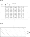
FIG. 3 is a view illustrating a top view of one surface of a display substrate according to an embodiment. -
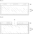
FIG. 4 is a view illustrating a cross-sectional view of a display substrate according to an embodiment. -
FIG. 5 is a view illustrating a cross-sectional view of a display substrate on which a photosensitive material is formed according to an embodiment. -
FIG. 6 is a view illustrating a cross-sectional view of a display substrate from which a photosensitive material in a pattern region is removed according to an embodiment. -
FIGS. 7 and8 are graphs showing atomic concentrations of base materials according to Exemplary Embodiment and Comparative Example. -
FIGS. 9 and10 are graphs showing a distribution of bonding states of atoms of surface layers of the base materials according to the Exemplary Embodiment and the Comparative Example. -
FIGS. 11 and 12 are views showing a degree to which an oxide layer of the base material according to the Exemplary Embodiment and the Comparative Example is peeled off. -
FIGS. 13 and14 are photographs for describing quality of etching after pattern formation of the base material according to the Exemplary Embodiment and the - Hereinafter, embodiments of the present invention will be described in detail with reference to the accompanying drawings. However, the spirit and scope of the present invention is not limited to a part of the embodiments described, and may be implemented in various other forms, and within the spirit and scope of the present invention, one or more of the elements of the embodiments may be selectively combined and replaced.
- In addition, unless expressly otherwise defined and described, the terms used in the embodiments of the present invention (including technical and scientific terms may be construed the same meaning as commonly understood by one of ordinary skill in the art to which this invention belongs, and the terms such as those defined in commonly used dictionaries may be interpreted as having a meaning that is consistent with their meaning in the context of the relevant art.
- In addition, the terms used in the embodiments of the present invention are for describing the embodiments and are not intended to limit the present invention. In this specification, the singular forms may also include the plural forms unless specifically stated in the phrase, and may include at least one of all combinations that may be combined in A, B, and C when described in "at least one (or more) of A (and), B, and C".
- Further, in describing the elements of the embodiments of the present invention, the terms such as first, second, A, B, (A, and (b) may be used. These terms are only used to distinguish the elements from other elements, and the terms are not limited to the essence, order, or order of the elements.
- In addition, when an element is described as being "connected", "coupled", or "connected" to another element, it may include not only when the element is directly "connected" to, "coupled" to, or "connected" to other elements, but also when the element is "connected", "coupled", or "connected" by another element between the element and other elements.
- Further, when described as being formed or disposed "on (over)" or "under (below)" of each element, the "on (over)" or "under (below)" may include not only when two elements are directly connected to each other, but also when one or more other elements are formed or disposed between two elements.
- Furthermore, when expressed as "on (over)" or "under (below)", it may include not only the upper direction but also the lower direction based on one element.
- Hereinafter, a display substrate according to an embodiment will be described with reference to drawings.
- Referring to
FIGS. 1 to 3 , a display substrate according to an embodiment includes abase material 100. - The
base material 100 may include metals, metal alloys, plastics, composite materials (e.g., carbon fiber reinforced plastics, magnetic or conductive materials, glass fiber reinforced materials, etc.), ceramics, sapphire, glass, and the like. As an example, thebase material 100 may include stainless steel (SUS). - Referring to
FIGS. 1 and2 , thebase material 100 may be bent in one direction. Specifically, thebase material 100 including afirst surface 1S and a second surface 2S may be folded in a direction in which any one of thefirst surface 1S and the second surface 2S faces each other with respect to a folding axis. - At this time, in case of the
base material 100, since thebase material 100 has both rigidity and ductility, compressive stress may be generated while bending in one direction, and there is a problem that cracks occur in thebase material 100 in a region in which the compressive stress is large. - Referring to
FIG. 3 , in order to solve such a problem, a plurality of patterns may be formed in one region of thebase material 100. Specifically, patterns P including a plurality of grooves or holes H may be formed in one region of thebase material 100. - Such patterns P may be formed in at least one region of a folding portion and an unfolding portion of the
base material 100. - In addition, a plurality of hinge portions HN may be formed at both ends of the
base material 100 to easily bend thebase material 100. - The patterns P and the hinge portions HN may be formed through exposure, development, and etching processes after forming a photosensitive material on the
base material 100. - In this case, the photosensitive material may be formed on a
surface portion 110 on thebase material 100, and thesurface portion 110 may be etched together when etching thebase material 100. - The
surface portion 110 may be formed on a surface of thebase material 100 to serve as a protective layer to prevent corrosion of the base material due to external oxygen. - Meanwhile, when the
surface portion 110 is over-etched during the etching process, since the surface portion does not remain in an over-etched region, crevice corrosion may occur between thebase material 100 and the photosensitive material. - In addition, a contact region between the surface portion and the photosensitive material may be reduced, and adhesion between the surface portion and the photosensitive material may be deteriorated, and thus the photosensitive material may be peeled off.
- Accordingly, the reliability and durability of the display substrate may be degraded, and a pattern having an incorrect size and shape is formed, and thus stress distribution by the pattern during folding may not be performed effectively.
- A display substrate according to an embodiment described below may prevent an over-etching of a surface portion generated during such an etching process to prevent corrosion, thereby forming a more precise pattern.
- Hereinafter, a display substrate according to an embodiment will be described in detail with reference to
FIGS. 4 to 14 . - Referring to
FIG. 4 , thedisplay substrate 1000 may include abase material 100. - As described above, the
base material 100 may include a material having rigidity and ductility. For example, thebase material 100 may include stainless steel (SUS). - Specifically, the
base material 100 may include at least one material of carbon (C), silicon (Si), manganese (Mn), phosphorus (P), sulfur (S), chromium (Cr), nickel (Ni), and iron (Fe). - The
base material 100 may include stainless steel (SUS) including about 10 wt% or more of chromium. More specifically, thebase material 100 may include stainless steel (SUS) including about 11 wt% to about 20 wt% of chromium. - Specifically, the
base material 100 may include stainless steel (SUS) containing about 0.15 wt% or less of carbon, about 1 wt% or less of silicon, about 2 wt% or less of manganese, about 0.045 wt% or less of phosphorus, about 0.03 wt% or less of sulfur, about 6 wt% to about 8 wt% of nickel, and iron as a balance. - The
base material 100 may include two regions defined by depth. In detail, thebase material 100 may be defined as a region of asurface portion 110 defined as a region from a surface S of thebase material 100 to 5 nm in the thickness direction of thebase material 100 and a region of acentral portion 120 inside of the surface portion. - As described above, the
base material 100 includes various compositions, but most of the content is made of iron (Fe). - Accordingly, the
base material 100 may combine with oxygen in the air in a natural state to form an oxide film on the surface thereof. That is, thesurface portion 110 may be defined as a surface oxide film formed on the surface of thebase material 100. - The
surface portion 110 may be formed on the entire surface of thebase material 100. That is, it may be formed on an upper surface, a lower surface, and side surfaces of the base material exposed to the outside. - Accordingly, the
surface portion 110 may be formed in a shape surrounding thecentral portion 120. - Meanwhile, the
surface portion 110 may be formed in a constant thickness. For example, thesurface portion 110 may have a thickness of about 10 nm to about 100 nm in a thickness direction of thebase material 100. - Meanwhile, referring to
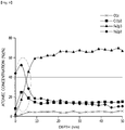
FIG. 5 , aphotosensitive material 200 such as a photoresist may be applied on thebase material 100, that is, on thesurface portion 110 in order to form a pattern having a hole or groove shape in one region of thebase material 100. - Subsequently, as shown in
FIG. 6 , thephotosensitive material 200 of a region EA to be etched through exposure and development processes may be removed. - Subsequently, the region from which the
photosensitive material 200 has been removed may be etched by an etching solution capable of etching thebase material 100. In detail, thesurface portion 110 and thecentral portion 120 may be etched together by the etching solution. In this case, when thesurface portion 110 is over-etched by the etching solution, adhesion between thesurface portion 110 and thephotosensitive material 200 may be deteriorated, and corrosion may occur in a gap portion. - The
display substrate 1000 according to the embodiment may control the composition of thesurface portion 110 in order to prevent deteriorating of the adhesion between the surface portion and the photosensitive material and corrosion. - Specifically, the
surface portion 110 may include iron oxides such as FeO and Fe2O3 and chromium oxide of Cr2O3. Thedisplay substrate 1000 according to the embodiment may solve the above problems by controlling atomic concentrations of chromium and iron atoms of thesurface portion 110. - Specifically, the
surface portion 110 may have a higher ratio of chromium atoms to iron atoms (Cr/Fe) than that of thecentral portion 120. In detail, thesurface portion 110 may have a ratio of chromium atoms to iron atoms (Cr/Fe) of about 0.7 or more. - That is, the
surface portion 110 may include a region in which the ratio of chromium atoms to iron atoms (Cr/Fe) is 0.7 or more. For example, the ratio of chromium atoms to iron atoms (Cr/Fe) may be 0.7 or more in at least one of the entire regions of thesurface portion 110. - In addition, the ratio of chromium atoms to iron atoms (Cr/Fe) may be 1 or more in at least one of the entire regions of the
surface portion 110. - In addition, the ratio of chromium atoms (Cr/Fe) to iron atoms may be 0.7 to 3.2 in at least one of the entire regions of the
surface portion 110. - For example, the
surface portion 110 may have a ratio of chromium atoms to iron atoms (Cr/Fe) of 1 or more at a depth from the surface of thebase material 100 to 3 nm in the depth direction of thebase material 100. - In addition, the
surface portion 110 may have a ratio of chromium atoms to iron atoms (Cr/Fe) of 0.7 or more at a depth from 3 nm to 5 nm in the depth direction of thebase material 100 from the surface of thebase material 100. - That is, the ratio of chromium atoms to iron atoms (Cr/Fe) may be higher as the
surface portion 110 is closer to the surface of thebase material 100. - That is, the ratio of chromium atoms to iron atoms (Cr/Fe) may be gradually increased as the
surface portion 110 is closer to the surface of thebase material 100. - That is, the ratio of chromium atoms to iron atoms (Cr/Fe) in the entire region of the
surface portion 110 may be 0.7 or more. - Accordingly, the
surface portion 110 may be a chromium-rich region having a higher content of chromium (Cr) than thecentral portion 120, and may include a chromium-rich region. - Such a chromium-rich region of the
surface portion 110 may be artificially formed. That is, the surface and oxygen in the air are combined on thebase material 100 to form an oxide layer by natural oxidation first, and the oxide layer is subjected to an acid treatment with a solution such as hydrochloric acid and a heat treatment to change one region of thesurface portion 110, that is, at least one region of thesurface portion 110 into a chromium-rich region. - Since chromium (Cr) or a chromium oxide film has better corrosion resistance than iron (Fe) or an iron oxide film, the
surface portion 110 may be prevented from being over-etched inward by an etching solution or the like during an etching process. - That is, the
photosensitive material 200 is adhered to thesurface portion 110, and accordingly, it is possible to prevent thesurface portion 110 from being over-etched by the etchant or the like during an etching process by adjusting the composition of thesurface portion 110 to a chromium-rich state. In addition, it is possible to prevent a deterioration in adhesion between thesurface portion 110 and thephotosensitive material 200 due to over-etching of the surface portion. - Meanwhile, the ratio of chromium atoms to iron atoms (Cr/Fe) at the
central portion 120 may be smaller than that at thesurface portion 110. - Specifically, the
central portion 120 may have a ratio of chromium atoms to iron atoms (Cr/ Fe) of less than 1. In detail, the ratio of chromium atoms to iron atoms (Cr/Fe) in thecentral portion 120 may be 0.3 to 0.6. That is, thecentral portion 120 may include a region in which the ratio of chromium atoms to iron atoms (Cr/Fe) is 0.3 to 0.6. - Accordingly, the
central portion 120 may be in an iron-rich state unlike thesurface portion 110. When the ratio of chromium atoms to iron atoms (Cr/Fe) in thecentral portion 120 exceeds 0.6, the corrosion resistance in thecentral portion 120 is increased to decrease an etching rate, and accordingly, etching efficiency during the etching process may be lowered, and thus pattern formation may be difficult. - That is, in the
surface portion 110 adhered to the photosensitive material, the corrosion resistance of the surface portion may be increased to prevent over-etching, and in thecentral portion 120, the corrosion resistance may be relatively reduced as compared with the surface portion, and thus the composition of thebase material 100 may be controlled such that thebase material 100 is easily etched. - Meanwhile, the display substrate according to the embodiment may be defined as a region in which a curvature is generated by folding of the display substrate and a region in which the curvature is not generated without folding. The pattern may be formed in both the region in which the curvature is generated and the region in which the curvature is not generated. Alternatively, the pattern may be formed only in the region in which the curvature is generated. Accordingly, the
base material 100 may be divided into a region in which a pattern is formed and a region in which a pattern is not formed. - The chromium and iron concentrations of the surface portion may be controlled in both the region in which the pattern is formed and the region in which the pattern is not formed. Alternatively, the chromium and iron concentrations of the surface portion may be controlled only in the region in which the pattern is formed.
- That is, since over-etching of the photosensitive material occurs in the etching process of forming the pattern, a process time according to reforming of the surface portion may be reduced by controlling the concentration of chromium and iron atoms only in the region in which the pattern is formed in the region of the base material.
- In the above description, the description has been made focusing on that the
display substrate 1000 is warped, but the embodiment is not limited thereto, and the embodiment may be applied when forming a pattern on thedisplay substrate 1000 which is not warped, or when forming a pattern on a base material used for a purpose other than the display substrate, for example, for a purpose such as a mask, and its application field is not limited to the above description. - Hereinafter, the present invention will be described in more detail with reference to Exemplary Embodiments and Comparative Examples. The Exemplary Embodiments are merely illustrative for describing the present invention in more detail. Therefore, the present invention is not limited to thereto.
- First, a stainless steel base material was prepared.
- The stainless steel base material contained 17 wt% of chromium.
- Subsequently, a surface of the stainless steel base material was bonded to oxygen in the air and spontaneously oxidized, and a surface oxidized region was formed on the surface of the base material. Subsequently, the surface of the stainless steel base material was subjected to an acid treatment using hydrochloric acid, and then heat-treated at a temperature of about 150 °C to reform the surface oxidized region of the base material.
- Subsequently, after a photoresist material was applied to the surface of the stainless steel base material, the photoresist material of a region to be patterned was removed through exposure and development processes.
- Meanwhile, a heat treatment process may be performed before and after the development process. In detail, reaction sensitivity may be increased through diffusion of a photosensitive agent through heat treatment after the exposure process, and surface roughness may be reduced by reducing the surface roughness of the surface portion after development through heat treatment after the development process.
- Subsequently, the stainless steel base material was etched using an etchant for etching a pattern formation region.
- Subsequently, an atomic concentration according to the depth from the surface of the stainless steel base material, a bonding state of atoms, and a degree of etching of the surface portion were measured.
- The same stainless steel base material as in the Exemplary Embodiment was prepared. Subsequently, the surface of the stainless steel base material was naturally oxidized, and a surface oxidized region was formed on the surface of the base material.
- Subsequently, after a photoresist material was applied to the surface of the base material, the photoresist material in a region in which a pattern was to be formed was removed through exposure and development processes.
- Subsequently, the stainless steel base material was etched using an etchant for etching a pattern formation region.
- That is, in the Comparative Example, the etching process was performed without performing the acid treatment and the heat treatment, unlike in the Exemplary Embodiment.
- Subsequently, an atomic concentration according to the depth from the surface of the stainless steel base material, a bonding state of atoms, and a degree of etching of the surface portion were measured.
-
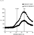
FIGS. 7 and8 are graphs showing an atomic concentration according to a depth from a surface of a stainless steel base material according to each of Exemplary Embodiment and Comparative Example measured by X-ray photoelectron spectroscopy (XPS). - Referring to
FIG. 7 , it may be seen that the base material according to the Comparative Example has a higher iron content than a chromium content at a depth from the surface (0 nm) to about 5 nm. That is, it may be seen that the base material according to the Comparative Example is in an iron-rich state having a high iron content at a depth from the surface (0 nm) to about 5 nm. - Referring to
FIG. 8 , it may be seen that the base material according to the Exemplary Embodiment has a higher chromium content than an iron content at a depth from the surface (0 nm) to about 5 nm. That is, it may be seen that the base material according to the Exemplary Embodiment is in a chromium-rich state having a high chromium content at a depth from the surface (0 nm) to about 5 nm. - The atomic concentration according to the depth of the base material according to the Exemplary Embodiment may be as shown in Table 1 below.
[Table 1] Depth (nm) Atomic concentration (%) Ols Cr2P3 Fe2P3 Ni2P3 0 51.3414 14.0089 4.4374 0.1224 3 4936837 25.6722 21.1005 2.1805 5 39.8000 20.3000 29.0000 10.90000 6 22.2638 18.9456 53.8546 4.9361 9 11.9097 14.4952 67.3275 6.0810 12 9.4319 14.3277 70.5415 3.9239 15 8.0446 13.8450 70.4111 4.7304 18 7.3511 13.8165 73.5573 5.1607 21 6.0022 14.4993 73.0769 5.1723 24 5.2749 15.1194 73.9616 5.6441 27 5.6255 16.2105 72.9753 5.1478 30 5.5839 14.6037 74.8789 4.9336 33 4.5958 15.2280 72.8422 5.0024 36 3.1684 15.9637 75.9920 4.8759 39 3.9479 17.0497 72.5544 5.1806 42 2.8363 15.2671 75.2987 5.4548 45 2.9084 16.2561 75.4045 5.0812 48 1.4864 1634783 76.4167 5.6186 51 2.8772 16.7165 75.3340 5.0680 - Referring to
FIG. 8 and Table 1, it may be seen that the base material according to the Exemplary Embodiment has a chromium-to-iron ratio (Cr/Fe) of 0.7 or more at a depth from the surface (0 nm) to about 5 nm. In addition, it may be seen that the chromium-to-iron ratio (Cr/Fe) is less than 0.7 from a depth of about 5 nm of the base material. - That is, at a depth from the surface (0 nm) which is a region in which the photosensitive material is adhered to the surface of the base material to about 5 nm, it is possible to prevent the surface portion from being over-etched during the etching process by increasing an amount of chromium having strong corrosion resistance. Accordingly, it is possible to prevent adhesion between the surface portion and the photosensitive material from being deteriorated due to over-etching, and prevent corrosion from occurring in a region to be over-etched.
- In addition, the etching process may be performed smoothly by reducing the amount of chromium having strong corrosion resistance and increasing the iron content from the depth of 5 nm of the base material, thereby forming a pattern more precisely.
-
FIGS. 9 and10 are graphs showing bonding states of chromium and iron atoms according to the Exemplary Embodiment and the Comparative Example measured at a region of 3 nm from the surface of the base material in the depth direction, that is, at a distance of 3 nm spaced apart from the surface of the base material, which are measured through bonding energy analysis. - Referring to
FIG. 9 , it may be seen that in the base material according to the Exemplary Embodiment, a ratio of chromium oxide having strong corrosion resistance on the surface portion is increased nearly twice as compared with the Comparative Example. - In addition, referring to
FIG. 10 , it may be seen that in the base material according to the Exemplary Embodiment, a ratio of the iron oxide film on the surface portion is similar to that of the Comparative Example. - That is, in the base material according to the Exemplary Embodiment is in a chromium-rich state in which a chromium content is high at a depth from the surface (0 nm) to about 5 nm, and particularly, since chromium atoms remain in a chromium oxide state having strong corrosion resistance, it is possible to effectively prevent the surface oxide layer from being over-etched during the etching process.
-
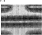
FIGS. 11 to 14 are cross-sectional views and photographs showing a degree to which the base material is etched during the etching process of the base material according to the Exemplary Embodiment and Comparative Example. - Referring to
FIG. 11 , in a display substrate according to the Comparative Example, it may be seen that a region FA in which a surface portion is etched inward during an etching process is large. On the other hand, referring toFIG. 12 , in a display substrate according to the Exemplary Embodiment, it may be seen that a region FA in which a surface portion is etched inward during an etching process is small. - That is, in the display substrate according to the Comparative Example, as shown in
FIG. 13 , the region FA in which the surface portion is etched inward is increased, and corrosion may occur in the region FA in which the surface portion is etched inward. In addition, it may be seen that the surface portion is over-etched inward, a contact region between the photosensitive material and the surface portion is reduced, and adhesion between the photosensitive material and the base material is deteriorated. - However, in the display substrate according to the Exemplary Embodiment, as shown in
FIG. 14 , it is possible to prevent corrosion from occurring in the region FA in which the surface portion is etched inward by minimizing the region FA in which the surface portion is etched inward. In addition, it is possible to prevent the contact region between the surface portion and the photosensitive material from being reduced by minimizing the region in which the surface portion is etched inward, and accordingly, it is possible to prevent adhesion between the photosensitive material and the base material from being deteriorated. - In the display substrate according to the embodiment, it is possible to prevent crevice corrosion generated when the surface portion is over-etched during etching of the base material and deterioration in adhesion to the photosensitive layer by controlling the atomic concentration of the surface portion of the base material.
- Specifically, the concentration of chromium oxide of the surface portion in contact with the photosensitive layer may be increased by reforming the surface portion.
- Accordingly, the corrosion resistance of the surface portion in the surface portion may be increased by increasing the content of chromium oxide in the surface portion.
- Accordingly, it is possible to minimize a phenomenon that the surface portion is over-etched inward during the etching process, and prevent deterioration in adhesion due to a decrease in a contact region between the surface portion and the photosensitive layer due to over-etching of the surface portion.
- In addition, it is possible to easily realize a desired pattern shape by smoothly proceeding the etching process by reducing the atomic concentration of chromium and increasing the atomic concentration of iron from a region other than the surface portion.
- The characteristics, structures, effects, and the like described in the above-described embodiments are included in at least one embodiment of the present invention, but are not limited to only one embodiment. Furthermore, the characteristic, structure, and effect illustrated in each embodiment may be combined or modified for other embodiments by a person skilled in the art. Accordingly, it is to be understood that such combination and modification are included in the scope of the present invention.
- In addition, although the above description been focused on the embodiments, the embodiments are merely examples and does not limit the present invention. It will be apparent to those skilled in the art that various modifications and applications not illustrated above may be made without departing from the essential features of the present embodiment. For example, elements of the exemplary embodiments described herein may be modified and realized. Also, it should be construed that differences related to such changes and applications are included in the scope of the present invention defined in the appended claims.
Claims (10)
- A display substrate comprisinga base material containing chromium and iron,wherein the base material includes a surface portion and a central portion,the surface portion is defined as a depth region from a surface of the base material to a depth of 5 nm in a thickness direction of the base material, anda ratio of chromium atoms to iron atoms (Cr/Fe) of the surface portion is greater than that of the central portion.
- The display substrate of claim 1, wherein the surface portion includes a region in which the ratio of chromium atoms to iron atoms (Cr/Fe) is 0.7 or more.
- The display substrate of claim 1, wherein the surface portion includes a region in which the ratio of chromium atoms to iron atoms (Cr/Fe) is 1 or more.
- The display substrate of claim 1, wherein the surface portion is a region in which the ratio of chromium atoms to iron atoms (Cr/Fe) is 0.7 or more.
- The display substrate of claim 1, wherein the central portion includes a region in which the ratio of chromium atoms to iron atoms (Cr/Fe) is 0.3 to 0.6.
- The display substrate of claim 1, wherein the ratio of chromium atoms to iron atoms (Cr/Fe) at the surface portion increases toward the surface of the base material.
- The display substrate of claim 1, wherein the base material includes 11 wt% to 20 wt% of chromium with respect to the total composition of the base material.
- The display substrate of claim 1, wherein the chromium atoms of the surface portion are included in a chromium oxide state.
- The display substrate of claim 8, wherein the base material includes a folding region that is bent in one direction, and in the folding region, the ratio of chromium atoms to iron atoms (Cr/Fe) of the surface portion is greater than that of the central portion.
- The display substrate of claim 9, wherein a hole or a groove is formed in the folding region of the base material.
Applications Claiming Priority (2)
| Application Number | Priority Date | Filing Date | Title |
|---|---|---|---|
| KR1020190009764A KR102665422B1 (en) | 2019-01-25 | 2019-01-25 | Substrate for display |
| PCT/KR2020/001049 WO2020153732A1 (en) | 2019-01-25 | 2020-01-22 | Substrate for display |
Publications (3)
| Publication Number | Publication Date |
|---|---|
| EP3916704A1 true EP3916704A1 (en) | 2021-12-01 |
| EP3916704A4 EP3916704A4 (en) | 2022-09-21 |
| EP3916704B1 EP3916704B1 (en) | 2024-08-07 |
Family
ID=71736410
Family Applications (1)
| Application Number | Title | Priority Date | Filing Date |
|---|---|---|---|
| EP20744548.7A Active EP3916704B1 (en) | 2019-01-25 | 2020-01-22 | Substrate for display |
Country Status (7)
| Country | Link |
|---|---|
| US (2) | US12175895B2 (en) |
| EP (1) | EP3916704B1 (en) |
| JP (2) | JP7155431B2 (en) |
| KR (2) | KR102665422B1 (en) |
| CN (2) | CN116072002B (en) |
| TW (1) | TWI837283B (en) |
| WO (1) | WO2020153732A1 (en) |
Family Cites Families (41)
| Publication number | Priority date | Publication date | Assignee | Title |
|---|---|---|---|---|
| JP2985334B2 (en) * | 1991-03-28 | 1999-11-29 | 凸版印刷株式会社 | Intaglio production method |
| US6208400B1 (en) * | 1996-03-15 | 2001-03-27 | Canon Kabushiki Kaisha | Electrode plate having metal electrodes of aluminum or nickel and copper or silver disposed thereon |
| DE19882178B4 (en) * | 1997-11-12 | 2004-08-05 | Daido Steel Co. Ltd., Nagoya | Stainless steel coated with intermetallic compound and method of manufacturing the same |
| JP2000302450A (en) * | 1999-04-14 | 2000-10-31 | Nippon Sheet Glass Co Ltd | Metal oxide film raw material and method for producing metal oxide film using the same |
| JP4442030B2 (en) * | 2000-05-31 | 2010-03-31 | 日本精工株式会社 | Method for manufacturing rolling support device |
| SE517894C2 (en) * | 2000-09-04 | 2002-07-30 | Sandvik Ab | FeCrAl alloy |
| CA2373344C (en) * | 2001-02-28 | 2012-03-20 | Daido Tokushuko Kabushiki Kaisha | Corrosion-resistant metallic member, metallic separator for fuel cell comprising the same, and process for production thereof |
| JP2004061844A (en) * | 2002-07-29 | 2004-02-26 | Hitachi Metals Ltd | Ag ALLOY FILM FOR DISPLAY DEVICE, Ag ALLOY REFLECTING FILM FOR DISPLAY DEVICE, FLAT PANEL DISPLAY DEVICE AND SPUTTERING TARGET MATERIAL FOR Ag ALLOY FILM DEPOSITION |
| KR20080023612A (en) | 2006-09-11 | 2008-03-14 | 엘지.필립스 엘시디 주식회사 | Flat panel display device and manufacturing method thereof |
| JP4983379B2 (en) * | 2007-05-07 | 2012-07-25 | 愛知製鋼株式会社 | Surface-treated stainless steel with excellent design and corrosion resistance and manufacturing method thereof |
| KR101540163B1 (en) | 2008-05-16 | 2015-07-28 | 신닛테츠스미킹 마테리알즈 가부시키가이샤 | Stainless steel foil for a flexible display |
| JP2010258399A (en) * | 2009-03-31 | 2010-11-11 | Jx Nippon Mining & Metals Corp | Copper foil for printed wiring boards |
| JP2011014654A (en) * | 2009-06-30 | 2011-01-20 | Jx Nippon Mining & Metals Corp | Copper foil for printed wiring board |
| CN102576735B (en) * | 2009-09-30 | 2016-01-20 | 大日本印刷株式会社 | Substrate for flexible device, thin film transistor substrate for flexible device, flexible device, substrate for thin film element, thin film element, thin film transistor, method for manufacturing substrate for thin film element, method for manufacturing thin film element, and method for manufacturing thin film transistor |
| JP5732740B2 (en) | 2009-09-30 | 2015-06-10 | 大日本印刷株式会社 | Thin film transistor substrate for flexible device and flexible device |
| JP2011249148A (en) * | 2010-05-27 | 2011-12-08 | Jx Nippon Mining & Metals Corp | Fuel cell separator material, fuel cell separator using the same, fuel cell stack, and method of manufacturing fuel cell separator material |
| KR101722936B1 (en) | 2010-12-08 | 2017-04-04 | 엘지디스플레이 주식회사 | Manufacturing method of flexible display device |
| CN102543861B (en) * | 2010-12-17 | 2014-12-31 | 群创光电股份有限公司 | Formation method of array substrate |
| DE102012002514B4 (en) | 2011-02-23 | 2014-07-24 | VDM Metals GmbH | Nickel-chromium-iron-aluminum alloy with good processability |
| KR101888424B1 (en) | 2011-07-13 | 2018-08-17 | 엘지디스플레이 주식회사 | Liquid Crystal Display having fixing member for fixing Light Guide Panel |
| JP5529839B2 (en) * | 2011-12-22 | 2014-06-25 | 株式会社栗本鐵工所 | Stainless steel member, method for producing the same, separator for use in polymer electrolyte fuel cell, and method for producing the same |
| US8557397B2 (en) * | 2011-12-29 | 2013-10-15 | Arcanum Alloy Design Inc. | Metallurgically bonded stainless steel |
| CA2869032C (en) * | 2012-03-30 | 2016-07-05 | Tata Steel Ijmuiden B.V. | Coated substrate for packaging applications and a method for producing said coated substrate |
| ES2964848T3 (en) * | 2012-05-23 | 2024-04-09 | Lg Energy Solution Ltd | Electrode assembly manufacturing method |
| JP6091145B2 (en) * | 2012-10-10 | 2017-03-08 | 日新製鋼株式会社 | Surface-modified stainless steel sheet and manufacturing method thereof |
| PT2924131T (en) | 2014-03-28 | 2019-10-30 | Outokumpu Oy | AUSTENITIC STAINLESS STEEL WITH HIGH MANGANESE CONTENT |
| CN104979490A (en) | 2014-04-03 | 2015-10-14 | 海洋王照明科技股份有限公司 | Flexible organic light emission diode and preparation method thereof |
| RU2661133C2 (en) * | 2014-04-04 | 2018-07-11 | Арселормиттал | Multilayer substrate and method of its manufacture |
| US9544994B2 (en) | 2014-08-30 | 2017-01-10 | Lg Display Co., Ltd. | Flexible display device with side crack protection structure and manufacturing method for the same |
| JP6477233B2 (en) * | 2015-05-20 | 2019-03-06 | 新日鐵住金株式会社 | Austenitic stainless steel |
| US9983424B2 (en) * | 2015-06-08 | 2018-05-29 | Lg Display Co., Ltd. | Foldable display device |
| KR102385233B1 (en) | 2015-08-06 | 2022-04-12 | 삼성디스플레이 주식회사 | Display apparatus and method for manufacturing the same |
| KR101798406B1 (en) * | 2015-09-22 | 2017-11-17 | 주식회사 포스코 | Stainless steel for fuel cell separator and method of manufacturing the same |
| JP6772897B2 (en) * | 2016-03-28 | 2020-10-21 | 東洋製罐グループホールディングス株式会社 | Flexible device substrate and its manufacturing method |
| US10670892B2 (en) | 2016-04-22 | 2020-06-02 | E Ink Corporation | Foldable electro-optic display apparatus |
| CN106057667B (en) * | 2016-07-06 | 2019-02-05 | 京东方科技集团股份有限公司 | Method for producing film pattern, method for producing substrate, substrate, and display device |
| KR102343734B1 (en) | 2017-07-12 | 2021-12-28 | 삼성디스플레이 주식회사 | Display device |
| KR101834793B1 (en) | 2017-07-28 | 2018-03-06 | 엘지디스플레이 주식회사 | Flexible Display and Electronic Device Including the Same |
| CN208376156U (en) * | 2018-06-23 | 2019-01-15 | 佛山市环宇新型材料有限公司 | A kind of novel Coil Coating Products that antiageing effect is good |
| KR102146317B1 (en) * | 2018-11-29 | 2020-08-20 | 주식회사 포스코 | Ferritic stainless steel improved in corrosion resistance and manufacturing method thereof |
| KR102736380B1 (en) * | 2019-01-16 | 2024-12-02 | 삼성디스플레이 주식회사 | Display device and manufacturing method of the same |
-
2019
- 2019-01-25 KR KR1020190009764A patent/KR102665422B1/en active Active
-
2020
- 2020-01-21 TW TW109102284A patent/TWI837283B/en active
- 2020-01-22 EP EP20744548.7A patent/EP3916704B1/en active Active
- 2020-01-22 WO PCT/KR2020/001049 patent/WO2020153732A1/en not_active Ceased
- 2020-01-22 JP JP2021531678A patent/JP7155431B2/en active Active
- 2020-01-22 US US17/284,532 patent/US12175895B2/en active Active
- 2020-01-22 CN CN202211645237.6A patent/CN116072002B/en active Active
- 2020-01-22 CN CN202080011003.9A patent/CN113366560B/en active Active
-
2022
- 2022-10-05 JP JP2022161014A patent/JP7414925B2/en active Active
-
2024
- 2024-05-07 KR KR1020240060088A patent/KR102856400B1/en active Active
- 2024-11-18 US US18/950,767 patent/US20250078690A1/en active Pending
Also Published As
| Publication number | Publication date |
|---|---|
| CN116072002B (en) | 2025-11-25 |
| JP2022511834A (en) | 2022-02-01 |
| CN113366560A (en) | 2021-09-07 |
| KR20240065062A (en) | 2024-05-14 |
| KR102856400B1 (en) | 2025-09-08 |
| JP7155431B2 (en) | 2022-10-18 |
| WO2020153732A1 (en) | 2020-07-30 |
| JP7414925B2 (en) | 2024-01-16 |
| KR102665422B1 (en) | 2024-05-10 |
| TW202034035A (en) | 2020-09-16 |
| CN116072002A (en) | 2023-05-05 |
| EP3916704B1 (en) | 2024-08-07 |
| JP2023015034A (en) | 2023-01-31 |
| US12175895B2 (en) | 2024-12-24 |
| CN113366560B (en) | 2023-04-28 |
| US20210383732A1 (en) | 2021-12-09 |
| TWI837283B (en) | 2024-04-01 |
| KR20200092635A (en) | 2020-08-04 |
| EP3916704A4 (en) | 2022-09-21 |
| US20250078690A1 (en) | 2025-03-06 |
Similar Documents
| Publication | Publication Date | Title |
|---|---|---|
| EP1650600B1 (en) | Photomask blank, photomask and fabrication method thereof | |
| US20190081241A1 (en) | Mask for thin film deposition, and fabrication method thereof | |
| US20210340664A1 (en) | Metal mask material, method for manufacturing same, and metal mask | |
| TW201250780A (en) | Mask blank substrate, mask blank, exposure mask, mask blank substrate manufacturing method, and semiconductor manufacturing method | |
| JP6756796B2 (en) | Mask blanks, halftone masks, manufacturing method | |
| US20250078690A1 (en) | Substrate for display | |
| JP7513095B2 (en) | Stainless steel foil, spring for switch, substrate for flexible display, and method for manufacturing stainless steel foil | |
| JP2004039319A (en) | Metal mask | |
| Kim et al. | 75‐4: Invited Paper: FMM Materials and Manufacturing Process: Review of the Technical Issues | |
| EP0176344A1 (en) | Colour picture tube | |
| JP6987912B2 (en) | Mask blanks, phase shift mask, manufacturing method | |
| JP2004039628A (en) | Metal mask | |
| JP2000003845A (en) | Method of manufacturing mask for X-ray exposure | |
| JP7062377B2 (en) | Manufacturing method of phase shift mask and phase shift mask | |
| WO2024143061A1 (en) | Metal mask base material, metal mask, and metal mask manufacturing method | |
| WO2001038594A1 (en) | Fe-Ni BASED ALLOY FOR SEMI-TENSION MASK EXCELLENT IN MAGNETIC CHARACTERISTICS, AND SEMI-TENSION MASK AND COLOR CATHODE-RAY TUBE USING THE SAME | |
| JP2002294407A (en) | High cleanliness material for shadow mask material | |
| WO2024204556A1 (en) | Metal mask base material, production method for metal mask base material, and production method for metal mask | |
| JP6207006B2 (en) | Method for manufacturing phase shift mask | |
| JP2003073797A (en) | Oxidation treatment method for shadow mask | |
| WO2000070108A1 (en) | Material for shadow mask, shadow mask and color image receiving tube having the shadow mask incorporated therein | |
| JP3327902B2 (en) | Fe-Ni shadow mask material | |
| Sawada et al. | Development of austenitic stainless steel sheets for micro-fabrication | |
| JPH11273579A (en) | Plasma display barrier rib and band steel for back face plate | |
| JPH08316390A (en) | Fe-ni based material for electronic device and production thereof |
Legal Events
| Date | Code | Title | Description |
|---|---|---|---|
| STAA | Information on the status of an ep patent application or granted ep patent |
Free format text: STATUS: THE INTERNATIONAL PUBLICATION HAS BEEN MADE |
|
| PUAI | Public reference made under article 153(3) epc to a published international application that has entered the european phase |
Free format text: ORIGINAL CODE: 0009012 |
|
| STAA | Information on the status of an ep patent application or granted ep patent |
Free format text: STATUS: REQUEST FOR EXAMINATION WAS MADE |
|
| 17P | Request for examination filed |
Effective date: 20210429 |
|
| AK | Designated contracting states |
Kind code of ref document: A1 Designated state(s): AL AT BE BG CH CY CZ DE DK EE ES FI FR GB GR HR HU IE IS IT LI LT LU LV MC MK MT NL NO PL PT RO RS SE SI SK SM TR |
|
| DAV | Request for validation of the european patent (deleted) | ||
| DAX | Request for extension of the european patent (deleted) | ||
| A4 | Supplementary search report drawn up and despatched |
Effective date: 20220819 |
|
| RIC1 | Information provided on ipc code assigned before grant |
Ipc: H01L 51/00 20060101ALI20220815BHEP Ipc: G06F 1/16 20060101ALI20220815BHEP Ipc: G09F 9/30 20060101AFI20220815BHEP |
|
| GRAP | Despatch of communication of intention to grant a patent |
Free format text: ORIGINAL CODE: EPIDOSNIGR1 |
|
| STAA | Information on the status of an ep patent application or granted ep patent |
Free format text: STATUS: GRANT OF PATENT IS INTENDED |
|
| RIC1 | Information provided on ipc code assigned before grant |
Ipc: H04M 1/02 20060101ALN20240411BHEP Ipc: H10K 77/10 20230101ALI20240411BHEP Ipc: G06F 1/16 20060101ALI20240411BHEP Ipc: G09F 9/30 20060101AFI20240411BHEP |
|
| RIC1 | Information provided on ipc code assigned before grant |
Ipc: H04M 1/02 20060101ALN20240418BHEP Ipc: H10K 77/10 20230101ALI20240418BHEP Ipc: G06F 1/16 20060101ALI20240418BHEP Ipc: G09F 9/30 20060101AFI20240418BHEP |
|
| INTG | Intention to grant announced |
Effective date: 20240510 |
|
| RIC1 | Information provided on ipc code assigned before grant |
Ipc: H04M 1/02 20060101ALN20240430BHEP Ipc: H10K 77/10 20230101ALI20240430BHEP Ipc: G06F 1/16 20060101ALI20240430BHEP Ipc: G09F 9/30 20060101AFI20240430BHEP |
|
| GRAS | Grant fee paid |
Free format text: ORIGINAL CODE: EPIDOSNIGR3 |
|
| GRAA | (expected) grant |
Free format text: ORIGINAL CODE: 0009210 |
|
| STAA | Information on the status of an ep patent application or granted ep patent |
Free format text: STATUS: THE PATENT HAS BEEN GRANTED |
|
| AK | Designated contracting states |
Kind code of ref document: B1 Designated state(s): AL AT BE BG CH CY CZ DE DK EE ES FI FR GB GR HR HU IE IS IT LI LT LU LV MC MK MT NL NO PL PT RO RS SE SI SK SM TR |
|
| REG | Reference to a national code |
Ref country code: GB Ref legal event code: FG4D |
|
| REG | Reference to a national code |
Ref country code: CH Ref legal event code: EP |
|
| REG | Reference to a national code |
Ref country code: IE Ref legal event code: FG4D |
|
| REG | Reference to a national code |
Ref country code: DE Ref legal event code: R096 Ref document number: 602020035342 Country of ref document: DE |
|
| REG | Reference to a national code |
Ref country code: LT Ref legal event code: MG9D |
|
| REG | Reference to a national code |
Ref country code: NL Ref legal event code: MP Effective date: 20240807 |
|
| PG25 | Lapsed in a contracting state [announced via postgrant information from national office to epo] |
Ref country code: NO Free format text: LAPSE BECAUSE OF FAILURE TO SUBMIT A TRANSLATION OF THE DESCRIPTION OR TO PAY THE FEE WITHIN THE PRESCRIBED TIME-LIMIT Effective date: 20241107 |
|
| REG | Reference to a national code |
Ref country code: AT Ref legal event code: MK05 Ref document number: 1711853 Country of ref document: AT Kind code of ref document: T Effective date: 20240807 |
|
| PG25 | Lapsed in a contracting state [announced via postgrant information from national office to epo] |
Ref country code: NL Free format text: LAPSE BECAUSE OF FAILURE TO SUBMIT A TRANSLATION OF THE DESCRIPTION OR TO PAY THE FEE WITHIN THE PRESCRIBED TIME-LIMIT Effective date: 20240807 Ref country code: GR Free format text: LAPSE BECAUSE OF FAILURE TO SUBMIT A TRANSLATION OF THE DESCRIPTION OR TO PAY THE FEE WITHIN THE PRESCRIBED TIME-LIMIT Effective date: 20241108 Ref country code: PT Free format text: LAPSE BECAUSE OF FAILURE TO SUBMIT A TRANSLATION OF THE DESCRIPTION OR TO PAY THE FEE WITHIN THE PRESCRIBED TIME-LIMIT Effective date: 20241209 Ref country code: FI Free format text: LAPSE BECAUSE OF FAILURE TO SUBMIT A TRANSLATION OF THE DESCRIPTION OR TO PAY THE FEE WITHIN THE PRESCRIBED TIME-LIMIT Effective date: 20240807 Ref country code: PL Free format text: LAPSE BECAUSE OF FAILURE TO SUBMIT A TRANSLATION OF THE DESCRIPTION OR TO PAY THE FEE WITHIN THE PRESCRIBED TIME-LIMIT Effective date: 20240807 |
|
| PG25 | Lapsed in a contracting state [announced via postgrant information from national office to epo] |
Ref country code: BG Free format text: LAPSE BECAUSE OF FAILURE TO SUBMIT A TRANSLATION OF THE DESCRIPTION OR TO PAY THE FEE WITHIN THE PRESCRIBED TIME-LIMIT Effective date: 20240807 |
|
| PG25 | Lapsed in a contracting state [announced via postgrant information from national office to epo] |
Ref country code: LV Free format text: LAPSE BECAUSE OF FAILURE TO SUBMIT A TRANSLATION OF THE DESCRIPTION OR TO PAY THE FEE WITHIN THE PRESCRIBED TIME-LIMIT Effective date: 20240807 |
|
| PG25 | Lapsed in a contracting state [announced via postgrant information from national office to epo] |
Ref country code: AT Free format text: LAPSE BECAUSE OF FAILURE TO SUBMIT A TRANSLATION OF THE DESCRIPTION OR TO PAY THE FEE WITHIN THE PRESCRIBED TIME-LIMIT Effective date: 20240807 Ref country code: IS Free format text: LAPSE BECAUSE OF FAILURE TO SUBMIT A TRANSLATION OF THE DESCRIPTION OR TO PAY THE FEE WITHIN THE PRESCRIBED TIME-LIMIT Effective date: 20241207 |
|
| PG25 | Lapsed in a contracting state [announced via postgrant information from national office to epo] |
Ref country code: HR Free format text: LAPSE BECAUSE OF FAILURE TO SUBMIT A TRANSLATION OF THE DESCRIPTION OR TO PAY THE FEE WITHIN THE PRESCRIBED TIME-LIMIT Effective date: 20240807 |
|
| PG25 | Lapsed in a contracting state [announced via postgrant information from national office to epo] |
Ref country code: ES Free format text: LAPSE BECAUSE OF FAILURE TO SUBMIT A TRANSLATION OF THE DESCRIPTION OR TO PAY THE FEE WITHIN THE PRESCRIBED TIME-LIMIT Effective date: 20240807 Ref country code: RS Free format text: LAPSE BECAUSE OF FAILURE TO SUBMIT A TRANSLATION OF THE DESCRIPTION OR TO PAY THE FEE WITHIN THE PRESCRIBED TIME-LIMIT Effective date: 20241107 |
|
| PG25 | Lapsed in a contracting state [announced via postgrant information from national office to epo] |
Ref country code: RS Free format text: LAPSE BECAUSE OF FAILURE TO SUBMIT A TRANSLATION OF THE DESCRIPTION OR TO PAY THE FEE WITHIN THE PRESCRIBED TIME-LIMIT Effective date: 20241107 Ref country code: PT Free format text: LAPSE BECAUSE OF FAILURE TO SUBMIT A TRANSLATION OF THE DESCRIPTION OR TO PAY THE FEE WITHIN THE PRESCRIBED TIME-LIMIT Effective date: 20241209 Ref country code: PL Free format text: LAPSE BECAUSE OF FAILURE TO SUBMIT A TRANSLATION OF THE DESCRIPTION OR TO PAY THE FEE WITHIN THE PRESCRIBED TIME-LIMIT Effective date: 20240807 Ref country code: NO Free format text: LAPSE BECAUSE OF FAILURE TO SUBMIT A TRANSLATION OF THE DESCRIPTION OR TO PAY THE FEE WITHIN THE PRESCRIBED TIME-LIMIT Effective date: 20241107 Ref country code: NL Free format text: LAPSE BECAUSE OF FAILURE TO SUBMIT A TRANSLATION OF THE DESCRIPTION OR TO PAY THE FEE WITHIN THE PRESCRIBED TIME-LIMIT Effective date: 20240807 Ref country code: LV Free format text: LAPSE BECAUSE OF FAILURE TO SUBMIT A TRANSLATION OF THE DESCRIPTION OR TO PAY THE FEE WITHIN THE PRESCRIBED TIME-LIMIT Effective date: 20240807 Ref country code: IS Free format text: LAPSE BECAUSE OF FAILURE TO SUBMIT A TRANSLATION OF THE DESCRIPTION OR TO PAY THE FEE WITHIN THE PRESCRIBED TIME-LIMIT Effective date: 20241207 Ref country code: HR Free format text: LAPSE BECAUSE OF FAILURE TO SUBMIT A TRANSLATION OF THE DESCRIPTION OR TO PAY THE FEE WITHIN THE PRESCRIBED TIME-LIMIT Effective date: 20240807 Ref country code: GR Free format text: LAPSE BECAUSE OF FAILURE TO SUBMIT A TRANSLATION OF THE DESCRIPTION OR TO PAY THE FEE WITHIN THE PRESCRIBED TIME-LIMIT Effective date: 20241108 Ref country code: FI Free format text: LAPSE BECAUSE OF FAILURE TO SUBMIT A TRANSLATION OF THE DESCRIPTION OR TO PAY THE FEE WITHIN THE PRESCRIBED TIME-LIMIT Effective date: 20240807 Ref country code: ES Free format text: LAPSE BECAUSE OF FAILURE TO SUBMIT A TRANSLATION OF THE DESCRIPTION OR TO PAY THE FEE WITHIN THE PRESCRIBED TIME-LIMIT Effective date: 20240807 Ref country code: BG Free format text: LAPSE BECAUSE OF FAILURE TO SUBMIT A TRANSLATION OF THE DESCRIPTION OR TO PAY THE FEE WITHIN THE PRESCRIBED TIME-LIMIT Effective date: 20240807 Ref country code: AT Free format text: LAPSE BECAUSE OF FAILURE TO SUBMIT A TRANSLATION OF THE DESCRIPTION OR TO PAY THE FEE WITHIN THE PRESCRIBED TIME-LIMIT Effective date: 20240807 |
|
| PG25 | Lapsed in a contracting state [announced via postgrant information from national office to epo] |
Ref country code: DK Free format text: LAPSE BECAUSE OF FAILURE TO SUBMIT A TRANSLATION OF THE DESCRIPTION OR TO PAY THE FEE WITHIN THE PRESCRIBED TIME-LIMIT Effective date: 20240807 Ref country code: SM Free format text: LAPSE BECAUSE OF FAILURE TO SUBMIT A TRANSLATION OF THE DESCRIPTION OR TO PAY THE FEE WITHIN THE PRESCRIBED TIME-LIMIT Effective date: 20240807 |
|
| PG25 | Lapsed in a contracting state [announced via postgrant information from national office to epo] |
Ref country code: EE Free format text: LAPSE BECAUSE OF FAILURE TO SUBMIT A TRANSLATION OF THE DESCRIPTION OR TO PAY THE FEE WITHIN THE PRESCRIBED TIME-LIMIT Effective date: 20240807 |
|
| PG25 | Lapsed in a contracting state [announced via postgrant information from national office to epo] |
Ref country code: CZ Free format text: LAPSE BECAUSE OF FAILURE TO SUBMIT A TRANSLATION OF THE DESCRIPTION OR TO PAY THE FEE WITHIN THE PRESCRIBED TIME-LIMIT Effective date: 20240807 |
|
| PG25 | Lapsed in a contracting state [announced via postgrant information from national office to epo] |
Ref country code: SK Free format text: LAPSE BECAUSE OF FAILURE TO SUBMIT A TRANSLATION OF THE DESCRIPTION OR TO PAY THE FEE WITHIN THE PRESCRIBED TIME-LIMIT Effective date: 20240807 |
|
| REG | Reference to a national code |
Ref country code: DE Ref legal event code: R097 Ref document number: 602020035342 Country of ref document: DE |
|
| PLBE | No opposition filed within time limit |
Free format text: ORIGINAL CODE: 0009261 |
|
| STAA | Information on the status of an ep patent application or granted ep patent |
Free format text: STATUS: NO OPPOSITION FILED WITHIN TIME LIMIT |
|
| 26N | No opposition filed |
Effective date: 20250508 |
|
| REG | Reference to a national code |
Ref country code: CH Ref legal event code: PL |
|
| PG25 | Lapsed in a contracting state [announced via postgrant information from national office to epo] |
Ref country code: SE Free format text: LAPSE BECAUSE OF FAILURE TO SUBMIT A TRANSLATION OF THE DESCRIPTION OR TO PAY THE FEE WITHIN THE PRESCRIBED TIME-LIMIT Effective date: 20240807 |
|
| PG25 | Lapsed in a contracting state [announced via postgrant information from national office to epo] |
Ref country code: MC Free format text: LAPSE BECAUSE OF FAILURE TO SUBMIT A TRANSLATION OF THE DESCRIPTION OR TO PAY THE FEE WITHIN THE PRESCRIBED TIME-LIMIT Effective date: 20240807 Ref country code: LU Free format text: LAPSE BECAUSE OF NON-PAYMENT OF DUE FEES Effective date: 20250122 |
|
| GBPC | Gb: european patent ceased through non-payment of renewal fee |
Effective date: 20250122 |
|
| PG25 | Lapsed in a contracting state [announced via postgrant information from national office to epo] |
Ref country code: BE Free format text: LAPSE BECAUSE OF NON-PAYMENT OF DUE FEES Effective date: 20250131 Ref country code: GB Free format text: LAPSE BECAUSE OF NON-PAYMENT OF DUE FEES Effective date: 20250122 |
|
| PG25 | Lapsed in a contracting state [announced via postgrant information from national office to epo] |
Ref country code: FR Free format text: LAPSE BECAUSE OF NON-PAYMENT OF DUE FEES Effective date: 20250131 |
|
| PG25 | Lapsed in a contracting state [announced via postgrant information from national office to epo] |
Ref country code: CH Free format text: LAPSE BECAUSE OF NON-PAYMENT OF DUE FEES Effective date: 20250131 |
|
| REG | Reference to a national code |
Ref country code: BE Ref legal event code: MM Effective date: 20250131 |
|
| PG25 | Lapsed in a contracting state [announced via postgrant information from national office to epo] |
Ref country code: IE Free format text: LAPSE BECAUSE OF NON-PAYMENT OF DUE FEES Effective date: 20250122 |
|
| PG25 | Lapsed in a contracting state [announced via postgrant information from national office to epo] |
Ref country code: IT Free format text: LAPSE BECAUSE OF FAILURE TO SUBMIT A TRANSLATION OF THE DESCRIPTION OR TO PAY THE FEE WITHIN THE PRESCRIBED TIME-LIMIT Effective date: 20240807 |
|
| PGFP | Annual fee paid to national office [announced via postgrant information from national office to epo] |
Ref country code: DE Payment date: 20251222 Year of fee payment: 7 |
|
| PG25 | Lapsed in a contracting state [announced via postgrant information from national office to epo] |
Ref country code: RO Free format text: LAPSE BECAUSE OF FAILURE TO SUBMIT A TRANSLATION OF THE DESCRIPTION OR TO PAY THE FEE WITHIN THE PRESCRIBED TIME-LIMIT Effective date: 20240807 |