EP3916511A1 - Digital low-dropout regulator and method for operating a digital low-dropout regulator - Google Patents
Digital low-dropout regulator and method for operating a digital low-dropout regulator Download PDFInfo
- Publication number
- EP3916511A1 EP3916511A1 EP21173200.3A EP21173200A EP3916511A1 EP 3916511 A1 EP3916511 A1 EP 3916511A1 EP 21173200 A EP21173200 A EP 21173200A EP 3916511 A1 EP3916511 A1 EP 3916511A1
- Authority
- EP
- European Patent Office
- Prior art keywords
- voltage
- ldo regulator
- digital ldo
- digital
- pmos
- Prior art date
- Legal status (The legal status is an assumption and is not a legal conclusion. Google has not performed a legal analysis and makes no representation as to the accuracy of the status listed.)
- Pending
Links
- 238000000034 method Methods 0.000 title claims abstract description 19
- 230000004044 response Effects 0.000 claims abstract description 23
- 238000010586 diagram Methods 0.000 description 4
- 230000003287 optical effect Effects 0.000 description 3
- 239000004065 semiconductor Substances 0.000 description 3
- 230000032683 aging Effects 0.000 description 2
- 230000006870 function Effects 0.000 description 2
- 238000010438 heat treatment Methods 0.000 description 2
- 239000003990 capacitor Substances 0.000 description 1
- 238000004590 computer program Methods 0.000 description 1
- 230000001419 dependent effect Effects 0.000 description 1
- 230000001105 regulatory effect Effects 0.000 description 1
- 239000007787 solid Substances 0.000 description 1
Images

Classifications
-
- G—PHYSICS
- G05—CONTROLLING; REGULATING
- G05F—SYSTEMS FOR REGULATING ELECTRIC OR MAGNETIC VARIABLES
- G05F1/00—Automatic systems in which deviations of an electric quantity from one or more predetermined values are detected at the output of the system and fed back to a device within the system to restore the detected quantity to its predetermined value or values, i.e. retroactive systems
- G05F1/10—Regulating voltage or current
- G05F1/46—Regulating voltage or current wherein the variable actually regulated by the final control device is DC
- G05F1/56—Regulating voltage or current wherein the variable actually regulated by the final control device is DC using semiconductor devices in series with the load as final control devices
- G05F1/575—Regulating voltage or current wherein the variable actually regulated by the final control device is DC using semiconductor devices in series with the load as final control devices characterised by the feedback circuit
-
- G—PHYSICS
- G05—CONTROLLING; REGULATING
- G05F—SYSTEMS FOR REGULATING ELECTRIC OR MAGNETIC VARIABLES
- G05F1/00—Automatic systems in which deviations of an electric quantity from one or more predetermined values are detected at the output of the system and fed back to a device within the system to restore the detected quantity to its predetermined value or values, i.e. retroactive systems
- G05F1/10—Regulating voltage or current
- G05F1/46—Regulating voltage or current wherein the variable actually regulated by the final control device is DC
- G05F1/56—Regulating voltage or current wherein the variable actually regulated by the final control device is DC using semiconductor devices in series with the load as final control devices
- G05F1/561—Voltage to current converters
-
- G—PHYSICS
- G05—CONTROLLING; REGULATING
- G05F—SYSTEMS FOR REGULATING ELECTRIC OR MAGNETIC VARIABLES
- G05F1/00—Automatic systems in which deviations of an electric quantity from one or more predetermined values are detected at the output of the system and fed back to a device within the system to restore the detected quantity to its predetermined value or values, i.e. retroactive systems
- G05F1/10—Regulating voltage or current
- G05F1/46—Regulating voltage or current wherein the variable actually regulated by the final control device is DC
- G05F1/56—Regulating voltage or current wherein the variable actually regulated by the final control device is DC using semiconductor devices in series with the load as final control devices
- G05F1/59—Regulating voltage or current wherein the variable actually regulated by the final control device is DC using semiconductor devices in series with the load as final control devices including plural semiconductor devices as final control devices for a single load
- G05F1/595—Regulating voltage or current wherein the variable actually regulated by the final control device is DC using semiconductor devices in series with the load as final control devices including plural semiconductor devices as final control devices for a single load semiconductor devices connected in series
-
- G—PHYSICS
- G05—CONTROLLING; REGULATING
- G05F—SYSTEMS FOR REGULATING ELECTRIC OR MAGNETIC VARIABLES
- G05F1/00—Automatic systems in which deviations of an electric quantity from one or more predetermined values are detected at the output of the system and fed back to a device within the system to restore the detected quantity to its predetermined value or values, i.e. retroactive systems
- G05F1/10—Regulating voltage or current
- G05F1/46—Regulating voltage or current wherein the variable actually regulated by the final control device is DC
- G05F1/56—Regulating voltage or current wherein the variable actually regulated by the final control device is DC using semiconductor devices in series with the load as final control devices
- G05F1/59—Regulating voltage or current wherein the variable actually regulated by the final control device is DC using semiconductor devices in series with the load as final control devices including plural semiconductor devices as final control devices for a single load
Definitions
- a digital low-dropout (LDO) regulator which is also referred to as a DLDO regulator, converts an input voltage into an output voltage and can be used to provide a stable operating voltage to components of an integrated circuit (IC).
- a digital LDO regulator converts an input voltage into an output voltage and can be used to provide a stable operating voltage to components of an integrated circuit (IC).
- IC integrated circuit
- a variable supply voltage can result in the deviation of transistor current. Consequently, the deviation of transistor current can cause a large ripple voltage on the regulator output voltage and lead to reliability problems. Therefore, there is a need for a digital LDO regulator that can generate a stable output voltage under a variable supply voltage.
- a digital LDO regulator includes a clamp circuit configured to generate a clamp voltage in response to an input voltage of the digital LDO regulator, a gate driver circuit configured to generate a drive voltage in response to the input voltage and the clamp voltage, and at least one transistor device configured to generate an output voltage in response to the input voltage and the drive voltage.
- a clamp circuit configured to generate a clamp voltage in response to an input voltage of the digital LDO regulator
- a gate driver circuit configured to generate a drive voltage in response to the input voltage and the clamp voltage
- at least one transistor device configured to generate an output voltage in response to the input voltage and the drive voltage.
- the output voltage is constant.
- the at least one transistor device includes at least one PMOS power transistor.
- the gate driver circuit is electrically connected to a gate terminal of the at least one PMOS power transistor.
- the input voltage is applied to a source terminal of the at least one PMOS power transistor.
- a drain terminal of the at least one PMOS power transistor is electrically connected to an output terminal from which the output voltage is output.
- the clamp circuit includes transistor devices and current sources that are electrically connected to the transistor devices.
- the clamp circuit includes first and second PMOS transistors that are serially connected to the input voltage, a first current source electrically connected to the first and second PMOS transistors and to a fixed voltage, a third PMOS transistor electrically connected to the first and second PMOS transistors, to the first current source, and to the fixed voltage, and a second current source electrically connected between the input voltage and the third PMOS transistor.
- the gate driver circuit includes inverters.
- the digital LDO regulator includes a voltage comparator configured to compare a reference voltage with the output voltage to generate a comparison result.
- the digital LDO regulator includes a controller configured to control the at least one transistor device based on the comparison result.
- a digital LDO regulator includes a clamp circuit configured to generate a clamp voltage in response to an input voltage of the digital LDO regulator, a gate driver circuit configured to generate a drive voltage in response to the input voltage and the clamp voltage and at least one PMOS power transistor configured to generate a constant output voltage in response to the input voltage and the drive voltage, where the input voltage varies between a first voltage level and a second voltage level.
- the gate driver circuit is electrically connected to a gate terminal of the at least one PMOS power transistor, wherein the input voltage is applied to a source terminal of the at least one PMOS power transistor, and wherein a drain terminal of the at least one PMOS power transistor is electrically connected to an output terminal from which the constant output voltage is output.
- the clamp circuit includes transistor devices and a plurality of current sources that are electrically connected to the transistor devices.
- the clamp circuit includes first and second PMOS transistors that are serially connected to the input voltage, a first current source electrically connected to the first and second PMOS transistors and to a fixed voltage, a third PMOS transistor electrically connected to the first and second PMOS transistors, to the first current source, and to the fixed voltage, and a second current source electrically connected between the input voltage and the third PMOS transistor.
- the gate driver circuit includes inverters.
- a method for operating a digital LDO regulator involves generating a clamp voltage in response to an input voltage of the digital LDO regulator using a clamp circuit of the digital LDO regulator, generating a drive voltage in response to the input voltage and the clamp voltage using a gate driver circuit of the digital LDO regulator, and generating an output voltage in response to the input voltage and the drive voltage using at least one transistor device of the digital LDO regulator.
- the output voltage is constant.
- the input voltage varies between a first voltage level and a second voltage level.
- the at least one transistor device includes at least one PMOS power transistor.
- Fig. 1 is a schematic block diagram of a digital LDO regulator 100 in accordance with an embodiment of the invention.
- the digital LDO regulator 100 includes a voltage comparator 102, a controller 104, a clamp circuit 106, at least one gate driver circuit 108, and at least one transistor device that is implemented as at least one PMOS power transistor, "M 1 ,” ..., “M N ,” where N is an integer that is greater than zero.
- the digital LDO regulator converts an input voltage or a supply voltage, "V IN ,” into an output voltage, "V OUT ,” for a load 110, which may be electrically connected to a fixed voltage (e.g., electrical ground (zero volt)).
- the input and output voltages of the digital LDO regulator can be any suitable type of Direct Current (DC) voltages.
- the digital LDO regulator can be used to provide an operating voltage for components of an IC.
- the digital LDO regulator converts an input voltage that is from 1.2 Volts (V) to 1.98V into an output voltage of 0.8V.
- the input and output voltages of the digital LDO regulator are not limited by the example voltages.
- the digital LDO regulator is shown in Fig. 1 as including certain components, in some embodiments, the digital LDO regulator includes less or more components to implement less or more functionalities.
- the digital LDO regulator is shown in Fig.
- the digital LDO regulator may include one or more other semiconductor devices.
- the digital LDO regulator includes a decoupling capacitor 112 that is electrically connected to a fixed voltage (e.g., electrical ground (zero volt)).
- the voltage comparator 102 is configured to compare a reference voltage, "V REF ,” with the output voltage, V OUT , of the digital LDO regulator 100 or a scaled version of the output voltage, V OUT , to generate a comparison result.
- V REF a reference voltage
- the voltage comparator can be implemented using various voltage comparison techniques that are well-known in the art.
- the controller 104 is configured to control the at least one PMOS power transistor, M 1 , ..., M N , based on the comparison result from the voltage comparator 102.
- the controller may be implemented in hardware (e.g., circuit or circuits), software, firmware, or a combination thereof.
- the controller is implemented using a hardware processor, such as a microcontroller, a digital signal processor (DSP), or a central processing unit (CPU).
- the controller is configured to enable (i.e., turn on/conducting) or disable (i.e., turn off/not conducting) the at least one PMOS power transistor, M 1 , ..., M N of the digital LDO regulator 100.
- the at least one PMOS power transistor, M 1 , ..., M N works as one or more switches.
- the at least one PMOS power transistor, M 1 , ..., M N can be controlled (e.g., turned on) by the controller 104.
- the current on each power transistor of the digital LDO regulator may have a large deviation, which can cause a large ripple voltage on the output voltage of the digital LDO regulator.
- the resistance of each power transistor of a digital LDO regulator is generally low. Consequently, when the output voltage of the digital LDO regulator varies (e.g., increases), the digital LDO regulator may have large power current under high supply voltage, which can bring up large ripple on the output voltage of the digital LDO regulator, which is a key specification of the digital LDO regulator, reliability concerns, such as heating and aging issues, for the power transistors of the digital LDO regulator.
- the clamp circuit 106 is configured to generate a clamp voltage, "V GATE_RAIL ,” based on the input voltage, V IN , of the digital LDO regulator 100
- the at least one gate driver circuit 108 is configured to generate at least one drive voltage in response to the input voltage, V IN , of the digital LDO regulator 100 and the clamp voltage, V GATE_RAIL
- the at least one power transistor, M 1 , ..., M N is configured to generate the output voltage, V OUT , of the digital LDO regulator 100 in response to the input voltage, V IN , of the digital LDO regulator and the at least one drive voltage.
- the digital LDO regulator 100 uses the clamp circuit 106 to clamp the at least one PMOS power transistor, M 1 , .., M N , for example, to operate in the saturation region by clamping the source-gate of the at least one PMOS power transistor, M 1 , ..., M N to a constant voltage. Therefore, the current on each PMOS power transistor M 1 , ..., or M N can be less dependent from or even almost independent from the input voltage, V IN , of the digital LDO regulator 100. Consequently, compared to a digital LDO regulator without a clamp circuit, the digital LDO regulator 100 depicted in Fig.
- each power transistor works as a switch in the linear region. Because the at least one PMOS power transistor, M 1 , ..., M N in the digital LDO regulator 100 works in the saturation region instead of the linear region, the digital LDO regulator 100 depicted in Fig. 1 provides better Power Supply Ripple Rejection (PSRR) especially for high frequencies that are out of the loop bandwidth.
- PSRR Power Supply Ripple Rejection
- an overcurrent protection function is implemented in the digital LDO regulator 100 automatically such that the output short-to-ground current can be limited and constant when the digital LDO regulator 100 is shorted to ground, while the output short-to-ground current can be out of the normal range when a digital LDO regulator without a clamp circuit is shorted to ground.
- the digital LDO regulator 100 is shown in Fig. 1 as a PMOS-type digital LDO regulator, the invention is also applicable for NMOS-type digital LDO regulators.
- the clamp circuit 106 is designed based on the output voltage, V OUT , of the NMOS-type digital LDO regulator and the at least one gate driver circuit 108 operates between the clamp voltage and the output voltage, V OUT .
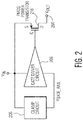
- Fig. 2 depicts a clamp circuit 206, a gate driver circuit 208 and a PMOS power transistor 216 that can be used in the digital LDO regulator 100 depicted in Fig. 1 .
- the clamp circuit 206, the gate driver circuit 208 and the PMOS power transistor 216 depicted in Fig. 2 are embodiments of the clamp circuit 106, the at least one gate driver circuit 108 and the at least one PMOS power transistor, M 1 , ..., M N of the digital LDO regulator 100 depicted in Fig. 1 .
- the clamp circuit 106, the at least one gate driver circuit 108 and the at least one PMOS power transistor, M 1 , ..., M N depicted in Fig. 1 are not limited to the embodiment shown in Fig. 2 .
- the input voltage or the supply voltage, V IN , to the digital LDO regulator 100 varies between around (e.g., ⁇ 30%) 1.2V and around (e.g., ⁇ 30%) 1.98V, and the output voltage, V OUT , is regulated to 0.8V.
- the clamp circuit 206 generates an internal voltage, V GATE_RAIL , based on the input voltage, V IN .
- the gate driver voltage that is generated by the gate driver circuit 208 is applied to the gate terminal, G, of the PMOS power transistor 216.
- the input voltage, V IN is applied to the source terminal, S, of the PMOS power transistor 216 and the drain terminal, D, of the PMOS power transistor 216 is electrically connected to an output terminal 260 from which the output voltage, V OUT , is output. Consequently, the gate driver circuit 208 operates between the input voltage, V IN , and the internal voltage, V GATE_RAIL .
- the source-gate voltage of the PMOS power transistor 216 is clamped to a constant value (i.e., from the input voltage, V IN , and the internal voltage, V GATE_RAIl ).
- the source-gate voltage of the PMOS power transistor 216 is clamped to the constant value and the PMOS power transistor 216 operates in the saturation region its power current can be almost independent on the input voltage, V IN .
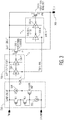
- Fig. 3 depicts a clamp circuit 306, at least one gate driver circuit 308-1, ..., 308-N, where N is an integer that is greater than zero, and at least one PMOS power transistor 316-1, ..., 316-N that can be used in the digital LDO regulator 100 depicted in Fig. 1 .
- the clamp circuit 306, the at least one gate driver circuit 308-1, ..., 308-N, and the at least one PMOS power transistor 316-1, .., 316-N depicted in Fig. 3 are embodiments of the clamp circuit 106, the at least one gate driver circuit 108 and the at least one PMOS power transistor, M 1 , ..., M N of the digital LDO regulator 100 depicted in Fig. 1 .
- the clamp circuit 106, the at least one gate driver circuit 108 and the at least one PMOS power transistor, M 1 , ..., M N depicted in Fig. 1 are not limited to the embodiment shown in Fig. 3 .
- the clamp circuit 306 includes a current source 332 configured to generate a constant current, I1, a current source 334 configured to generate a constant current, 12, two diodeconnected PMOS transistors, PM1, PM2, which are connected to a PMOS transistor, PM3, that acts as a source follower.
- the current source 332 and the PMOS transistors, PM3, are electrically connected to a fixed voltage, such as ground (0V).
- a fixed voltage such as ground (0V).
- the PMOS transistors, PM1, PM2, are connected to the input voltage, V IN
- the current source 332 is electrically connected to the PMOS transistors, PM1, PM2, and to ground
- the PMOS transistor, PM3, is electrically connected to the PMOS transistors, PM1, PM2, to the current source 332, and to ground
- the current source 334 is electrically connected between the input voltage, V IN , and the PMOS transistor, PM3.
- the clamp circuit 306 generates an internal voltage, V GATE_RAIL , based on the input voltage, V IN .
- the gate driver circuit 308-1 includes at least two inverters 336-1, 338-1 that operate between the input voltage, V IN , and the internal voltage, V GATE_RAIL .
- the driver voltage that is generated by the gate driver circuit 308-1 is applied to the gate terminal, G, of the PMOS power transistor 316-1.
- the input voltage, V IN is applied to the source terminal, S, of the PMOS power transistor 316-1 and the drain terminal, D, of the PMOS power transistor 316-1 is electrically connected to an output terminal 360 from which the output voltage, V OUT , is output.
- the gate driver circuit 308-N includes at least two inverters 336-N, 338-N that operate between the input voltage, V IN , and the internal voltage, V GATE_RAIL .
- the driver voltage that is generated by the gate driver circuit 308-N is applied to the gate terminal, G, of the PMOS power transistor 316-N.
- the input voltage, V IN is applied to the source terminal, S, of the PMOS power transistor 316-N and the drain terminal, D, of the PMOS power transistor 316-N is electrically connected to the output terminal 360 from which the output voltage, V OUT , is output.
- V DIFF V SG_PM 1 + V SG_PM 2 ⁇ V SG_PM 3 , where V SG_PM1 represents the source-gate voltage of the PMOS transistor, PM1, V SG_PM2 represents the source-gate voltage of the PMOS transistor, PM2, and V SG_PM3 represents the source-gate voltage of the PMOS transistor, PM3.
- the voltage difference, V DIFF , between the input voltage, V IN , and the internal voltage, V GATE_RAIL , is equal to the source-gate voltage, V SG_PM1 , of the PMOS transistor, PM1.
- the gate voltage of the PMOS power transistor 316-1 is pulled down to the internal voltage, V GATE_RAIL , by the gate driver circuit 308-1.
- the PMOS transistor, PM1, and the PMOS power transistor 316-1 work as a current mirror when the PMOS power transistor 316-1 operates in the saturation region (e.g., when the sourcedrain voltage, V SD , of the PMOS power transistor 316-1 is higher than a threshold).
- the current, I P1 , conducted by the PMOS power transistor 316-1 is constant.
- the PMOS power transistor 316-N and the gate driver circuit 308-N operate similarly to or identically with the PMOS power transistor 316-1 and the gate driver circuit 308-1, respectively.
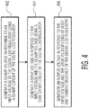
- Fig. 4 is a process flow diagram of a method for operating a digital LDO regulator in accordance with an embodiment of the invention.
- the digital LDO regulator may be similar to or the same as the digital LDO regulator 100 depicted in Fig. 1 .
- a clamp voltage is generated in response to an input voltage of the digital LDO regulator using a clamp circuit of the digital LDO regulator.
- a drive voltage is generated in response to the input voltage and the clamp voltage using a gate driver circuit of the digital LDO regulator.
- an output voltage is generated in response to the input voltage and the drive voltage using at least one transistor device of the digital LDO regulator.
- an embodiment of a computer program product includes a computer useable storage medium to store a computer readable program.
- the computer-useable or computer-readable storage medium can be an electronic, magnetic, optical, electromagnetic, infrared, or semiconductor system (or apparatus or device).
- Examples of non-transitory computer-useable and computer-readable storage media include a semiconductor or solid state memory, magnetic tape, a removable computer diskette, electrically erasable programmable read-only memory (EEPROM), a random access memory (RAM), a read-only memory (ROM), a rigid magnetic disk, and an optical disk.
- Current examples of optical disks include a compact disk with read only memory (CD-ROM), a compact disk with read/write (CD-R/W), and a digital video disk (DVD).
- embodiments of the invention may be implemented entirely in hardware or in an implementation containing both hardware and software elements.
- the software may include but is not limited to firmware, resident software, microcode, etc.
Landscapes
- Engineering & Computer Science (AREA)
- Physics & Mathematics (AREA)
- Electromagnetism (AREA)
- General Physics & Mathematics (AREA)
- Radar, Positioning & Navigation (AREA)
- Automation & Control Theory (AREA)
- Continuous-Control Power Sources That Use Transistors (AREA)
Abstract
Description
- A digital low-dropout (LDO) regulator, which is also referred to as a DLDO regulator, converts an input voltage into an output voltage and can be used to provide a stable operating voltage to components of an integrated circuit (IC). In a digital LDO regulator, a variable supply voltage can result in the deviation of transistor current. Consequently, the deviation of transistor current can cause a large ripple voltage on the regulator output voltage and lead to reliability problems. Therefore, there is a need for a digital LDO regulator that can generate a stable output voltage under a variable supply voltage.
- Embodiments of digital LDO regulators and methods for operating a digital LDO regulator are described. In an embodiment, a digital LDO regulator includes a clamp circuit configured to generate a clamp voltage in response to an input voltage of the digital LDO regulator, a gate driver circuit configured to generate a drive voltage in response to the input voltage and the clamp voltage, and at least one transistor device configured to generate an output voltage in response to the input voltage and the drive voltage. Other embodiments are also described.
- In an embodiment, the output voltage is constant.
- In an embodiment, the at least one transistor device includes at least one PMOS power transistor.
- In an embodiment, the gate driver circuit is electrically connected to a gate terminal of the at least one PMOS power transistor.
- In an embodiment, the input voltage is applied to a source terminal of the at least one PMOS power transistor.
- In an embodiment, a drain terminal of the at least one PMOS power transistor is electrically connected to an output terminal from which the output voltage is output.
- In an embodiment, the clamp circuit includes transistor devices and current sources that are electrically connected to the transistor devices.
- In an embodiment, the clamp circuit includes first and second PMOS transistors that are serially connected to the input voltage, a first current source electrically connected to the first and second PMOS transistors and to a fixed voltage, a third PMOS transistor electrically connected to the first and second PMOS transistors, to the first current source, and to the fixed voltage, and a second current source electrically connected between the input voltage and the third PMOS transistor.
- In an embodiment, the gate driver circuit includes inverters.
- In an embodiment, the digital LDO regulator includes a voltage comparator configured to compare a reference voltage with the output voltage to generate a comparison result.
- In an embodiment, the digital LDO regulator includes a controller configured to control the at least one transistor device based on the comparison result.
- In an embodiment, a digital LDO regulator includes a clamp circuit configured to generate a clamp voltage in response to an input voltage of the digital LDO regulator, a gate driver circuit configured to generate a drive voltage in response to the input voltage and the clamp voltage and at least one PMOS power transistor configured to generate a constant output voltage in response to the input voltage and the drive voltage, where the input voltage varies between a first voltage level and a second voltage level.
- In an embodiment, the gate driver circuit is electrically connected to a gate terminal of the at least one PMOS power transistor, wherein the input voltage is applied to a source terminal of the at least one PMOS power transistor, and wherein a drain terminal of the at least one PMOS power transistor is electrically connected to an output terminal from which the constant output voltage is output.
- In an embodiment, the clamp circuit includes transistor devices and a plurality of current sources that are electrically connected to the transistor devices.
- In an embodiment, the clamp circuit includes first and second PMOS transistors that are serially connected to the input voltage, a first current source electrically connected to the first and second PMOS transistors and to a fixed voltage, a third PMOS transistor electrically connected to the first and second PMOS transistors, to the first current source, and to the fixed voltage, and a second current source electrically connected between the input voltage and the third PMOS transistor.
- In an embodiment, the gate driver circuit includes inverters.
- In an embodiment, a method for operating a digital LDO regulator involves generating a clamp voltage in response to an input voltage of the digital LDO regulator using a clamp circuit of the digital LDO regulator, generating a drive voltage in response to the input voltage and the clamp voltage using a gate driver circuit of the digital LDO regulator, and generating an output voltage in response to the input voltage and the drive voltage using at least one transistor device of the digital LDO regulator.
- In an embodiment, the output voltage is constant.
- In an embodiment, the input voltage varies between a first voltage level and a second voltage level.
- In an embodiment, the at least one transistor device includes at least one PMOS power transistor.
- Other aspects and advantages of embodiments of the present invention will become apparent from the following detailed description, taken in conjunction with the accompanying drawings, depicted by way of example of the principles of the invention.
-
-
Fig. 1 is a schematic block diagram of a digital LDO regulator in accordance with an embodiment of the invention. -
Fig. 2 depicts a clamp circuit, a gate driver circuit, and a PMOS power transistor that can be used in the digital LDO regulator depicted inFig. 1 . -
Fig. 3 depicts a clamp circuit, at least one gate driver circuit, and at least one PMOS power transistor that can be used in the digital LDO regulator depicted inFig. 1 . -
Fig. 4 is a process flow diagram of a method for operating a digital LDO regulator in accordance with an embodiment of the invention. - Throughout the description, similar reference numbers may be used to identify similar elements.
- It will be readily understood that the components of the embodiments as generally described herein and illustrated in the appended figures could be arranged and designed in a wide variety of different configurations. Thus, the following detailed description of various embodiments, as represented in the figures, is not intended to limit the scope of the present disclosure, but is merely representative of various embodiments. While the various aspects of the embodiments are presented in drawings, the drawings are not necessarily drawn to scale unless specifically indicated.
- The described embodiments are to be considered in all respects only as illustrative and not restrictive. The scope of the invention is, therefore, indicated by the appended claims rather than by this detailed description. All changes which come within the meaning and range of equivalency of the claims are to be embraced within their scope.
- Reference throughout this specification to features, advantages, or similar language does not imply that all of the features and advantages that may be realized with the present invention should be or are in any single embodiment. Rather, language referring to the features and advantages is understood to mean that a specific feature, advantage, or characteristic described in connection with an embodiment is included in at least one embodiment. Thus, discussions of the features and advantages, and similar language, throughout this specification may, but do not necessarily, refer to the same embodiment.
- Furthermore, the described features, advantages, and characteristics of the invention may be combined in any suitable manner in one or more embodiments. One skilled in the relevant art will recognize, in light of the description herein, that the invention can be practiced without one or more of the specific features or advantages of a particular embodiment. In other instances, additional features and advantages may be recognized in certain embodiments that may not be present in all embodiments of the invention.
- Reference throughout this specification to "one embodiment," "an embodiment," or similar language means that a particular feature, structure, or characteristic described in connection with the indicated embodiment is included in at least one embodiment. Thus, the phrases "in one embodiment," "in an embodiment," and similar language throughout this specification may, but do not necessarily, all refer to the same embodiment.
-
Fig. 1 is a schematic block diagram of adigital LDO regulator 100 in accordance with an embodiment of the invention. In the embodiment depicted inFig. 1 , thedigital LDO regulator 100 includes avoltage comparator 102, acontroller 104, aclamp circuit 106, at least onegate driver circuit 108, and at least one transistor device that is implemented as at least one PMOS power transistor, "M1," ..., "MN," where N is an integer that is greater than zero. The digital LDO regulator converts an input voltage or a supply voltage, "VIN," into an output voltage, "VOUT," for aload 110, which may be electrically connected to a fixed voltage (e.g., electrical ground (zero volt)). The input and output voltages of the digital LDO regulator can be any suitable type of Direct Current (DC) voltages. The digital LDO regulator can be used to provide an operating voltage for components of an IC. In some embodiments, the digital LDO regulator converts an input voltage that is from 1.2 Volts (V) to 1.98V into an output voltage of 0.8V. However, the input and output voltages of the digital LDO regulator are not limited by the example voltages. Although the digital LDO regulator is shown inFig. 1 as including certain components, in some embodiments, the digital LDO regulator includes less or more components to implement less or more functionalities. For example, although the digital LDO regulator is shown inFig. 1 as including an array of PMOS power transistor(s), M1, ..., MN, in other embodiments, the digital LDO regulator may include one or more other semiconductor devices. In another example, in some embodiments, the digital LDO regulator includes adecoupling capacitor 112 that is electrically connected to a fixed voltage (e.g., electrical ground (zero volt)). - In the embodiment depicted in
Fig. 1 , thevoltage comparator 102 is configured to compare a reference voltage, "VREF," with the output voltage, VOUT, of thedigital LDO regulator 100 or a scaled version of the output voltage, VOUT, to generate a comparison result. The voltage comparator can be implemented using various voltage comparison techniques that are well-known in the art. - In the embodiment depicted in
Fig. 1 , thecontroller 104 is configured to control the at least one PMOS power transistor, M1, ..., MN, based on the comparison result from thevoltage comparator 102. The controller may be implemented in hardware (e.g., circuit or circuits), software, firmware, or a combination thereof. In an embodiment, the controller is implemented using a hardware processor, such as a microcontroller, a digital signal processor (DSP), or a central processing unit (CPU). In some embodiments, the controller is configured to enable (i.e., turn on/conducting) or disable (i.e., turn off/not conducting) the at least one PMOS power transistor, M1, ..., MN of thedigital LDO regulator 100. For example, the at least one PMOS power transistor, M1, ..., MN works as one or more switches. Depending on the difference between the output voltage, VOUT, of thedigital LDO regulator 100, or a scaled version of the output voltage, VOUT, and the reference voltage, VREF, the at least one PMOS power transistor, M1, ..., MN can be controlled (e.g., turned on) by thecontroller 104. - When a digital LDO regulator is used with a variable input voltage, such as in case the digital LDO regulator is powered by a battery, the current on each power transistor of the digital LDO regulator may have a large deviation, which can cause a large ripple voltage on the output voltage of the digital LDO regulator. In order to deliver enough power current under a low supply voltage, the resistance of each power transistor of a digital LDO regulator is generally low. Consequently, when the output voltage of the digital LDO regulator varies (e.g., increases), the digital LDO regulator may have large power current under high supply voltage, which can bring up large ripple on the output voltage of the digital LDO regulator, which is a key specification of the digital LDO regulator, reliability concerns, such as heating and aging issues, for the power transistors of the digital LDO regulator.
- In the embodiment depicted in
Fig. 1 , theclamp circuit 106 is configured to generate a clamp voltage, "VGATE_RAIL," based on the input voltage, VIN, of thedigital LDO regulator 100, the at least onegate driver circuit 108 is configured to generate at least one drive voltage in response to the input voltage, VIN, of thedigital LDO regulator 100 and the clamp voltage, VGATE_RAIL, and the at least one power transistor, M1, ..., MN is configured to generate the output voltage, VOUT, of thedigital LDO regulator 100 in response to the input voltage, VIN, of the digital LDO regulator and the at least one drive voltage. - In the embodiment depicted in
Fig. 1 , thedigital LDO regulator 100 uses theclamp circuit 106 to clamp the at least one PMOS power transistor, M1, .., MN, for example, to operate in the saturation region by clamping the source-gate of the at least one PMOS power transistor, M1, ..., MN to a constant voltage. Therefore, the current on each PMOS power transistor M1, ..., or MN can be less dependent from or even almost independent from the input voltage, VIN, of thedigital LDO regulator 100. Consequently, compared to a digital LDO regulator without a clamp circuit, thedigital LDO regulator 100 depicted inFig. 1 has a smaller ripple voltage on the output voltage, VOUT, and as a result, less possibility that heating and aging issues on the reliability of the at least one PMOS power transistor, M1, ..., MN can occur. In addition, in a digital LDO regulator without a clamp circuit, each power transistor works as a switch in the linear region. Because the at least one PMOS power transistor, M1, ..., MN in thedigital LDO regulator 100 works in the saturation region instead of the linear region, thedigital LDO regulator 100 depicted inFig. 1 provides better Power Supply Ripple Rejection (PSRR) especially for high frequencies that are out of the loop bandwidth. In addition, an overcurrent protection function is implemented in thedigital LDO regulator 100 automatically such that the output short-to-ground current can be limited and constant when thedigital LDO regulator 100 is shorted to ground, while the output short-to-ground current can be out of the normal range when a digital LDO regulator without a clamp circuit is shorted to ground. - Although the
digital LDO regulator 100 is shown inFig. 1 as a PMOS-type digital LDO regulator, the invention is also applicable for NMOS-type digital LDO regulators. When thedigital LDO regulator 100 is implemented as an NMOS-type digital LDO regulator, theclamp circuit 106 is designed based on the output voltage, VOUT, of the NMOS-type digital LDO regulator and the at least onegate driver circuit 108 operates between the clamp voltage and the output voltage, VOUT. -
Fig. 2 depicts aclamp circuit 206, agate driver circuit 208 and aPMOS power transistor 216 that can be used in thedigital LDO regulator 100 depicted inFig. 1 . Theclamp circuit 206, thegate driver circuit 208 and thePMOS power transistor 216 depicted inFig. 2 are embodiments of theclamp circuit 106, the at least onegate driver circuit 108 and the at least one PMOS power transistor, M1, ..., MN of thedigital LDO regulator 100 depicted inFig. 1 . However, theclamp circuit 106, the at least onegate driver circuit 108 and the at least one PMOS power transistor, M1, ..., MN depicted inFig. 1 are not limited to the embodiment shown inFig. 2 . In an embodiment, the input voltage or the supply voltage, VIN, to thedigital LDO regulator 100 varies between around (e.g., ±30%) 1.2V and around (e.g., ±30%) 1.98V, and the output voltage, VOUT, is regulated to 0.8V. However, the input and output voltages of thedigital LDO regulator 100 are not limited by the example voltages. Theclamp circuit 206 generates an internal voltage, VGATE_RAIL, based on the input voltage, VIN. The gate driver voltage that is generated by thegate driver circuit 208 is applied to the gate terminal, G, of thePMOS power transistor 216. The input voltage, VIN, is applied to the source terminal, S, of thePMOS power transistor 216 and the drain terminal, D, of thePMOS power transistor 216 is electrically connected to anoutput terminal 260 from which the output voltage, VOUT, is output. Consequently, thegate driver circuit 208 operates between the input voltage, VIN, and the internal voltage, VGATE_RAIL. When thePMOS power transistor 216 is turned on (i.e., conducting), the source-gate voltage of thePMOS power transistor 216 is clamped to a constant value (i.e., from the input voltage, VIN, and the internal voltage, VGATE_RAIl). When the source-gate voltage of thePMOS power transistor 216 is clamped to the constant value and thePMOS power transistor 216 operates in the saturation region its power current can be almost independent on the input voltage, VIN. -
Fig. 3 depicts aclamp circuit 306, at least one gate driver circuit 308-1, ..., 308-N, where N is an integer that is greater than zero, and at least one PMOS power transistor 316-1, ..., 316-N that can be used in thedigital LDO regulator 100 depicted inFig. 1 . Theclamp circuit 306, the at least one gate driver circuit 308-1, ..., 308-N, and the at least one PMOS power transistor 316-1, .., 316-N depicted inFig. 3 are embodiments of theclamp circuit 106, the at least onegate driver circuit 108 and the at least one PMOS power transistor, M1, ..., MN of thedigital LDO regulator 100 depicted inFig. 1 . However, theclamp circuit 106, the at least onegate driver circuit 108 and the at least one PMOS power transistor, M1, ..., MN depicted inFig. 1 are not limited to the embodiment shown inFig. 3 . In the embodiment depicted inFig. 3 , theclamp circuit 306 includes acurrent source 332 configured to generate a constant current, I1, acurrent source 334 configured to generate a constant current, 12, two diodeconnected PMOS transistors, PM1, PM2, which are connected to a PMOS transistor, PM3, that acts as a source follower. Thecurrent source 332 and the PMOS transistors, PM3, are electrically connected to a fixed voltage, such as ground (0V). In the embodiment depicted inFig. 3 , the PMOS transistors, PM1, PM2, are connected to the input voltage, VIN, thecurrent source 332 is electrically connected to the PMOS transistors, PM1, PM2, and to ground, the PMOS transistor, PM3, is electrically connected to the PMOS transistors, PM1, PM2, to thecurrent source 332, and to ground, and thecurrent source 334 is electrically connected between the input voltage, VIN, and the PMOS transistor, PM3. Theclamp circuit 306 generates an internal voltage, VGATE_RAIL, based on the input voltage, VIN. In the embodiment depicted inFig. 3 , the gate driver circuit 308-1 includes at least two inverters 336-1, 338-1 that operate between the input voltage, VIN, and the internal voltage, VGATE_RAIL. The driver voltage that is generated by the gate driver circuit 308-1 is applied to the gate terminal, G, of the PMOS power transistor 316-1. The input voltage, VIN, is applied to the source terminal, S, of the PMOS power transistor 316-1 and the drain terminal, D, of the PMOS power transistor 316-1 is electrically connected to anoutput terminal 360 from which the output voltage, VOUT, is output. The gate driver circuit 308-N includes at least two inverters 336-N, 338-N that operate between the input voltage, VIN, and the internal voltage, VGATE_RAIL. The driver voltage that is generated by the gate driver circuit 308-N is applied to the gate terminal, G, of the PMOS power transistor 316-N. The input voltage, VIN, is applied to the source terminal, S, of the PMOS power transistor 316-N and the drain terminal, D, of the PMOS power transistor 316-N is electrically connected to theoutput terminal 360 from which the output voltage, VOUT, is output. - In the embodiment depicted in
Fig. 3 , the voltage difference, VDIFF, between the input voltage, VIN, and the internal voltage, VGATE_RAIL, can be expressed as:

-
Fig. 4 is a process flow diagram of a method for operating a digital LDO regulator in accordance with an embodiment of the invention. The digital LDO regulator may be similar to or the same as thedigital LDO regulator 100 depicted inFig. 1 . Atblock 402, a clamp voltage is generated in response to an input voltage of the digital LDO regulator using a clamp circuit of the digital LDO regulator. Atblock 404, a drive voltage is generated in response to the input voltage and the clamp voltage using a gate driver circuit of the digital LDO regulator. Atblock 406, an output voltage is generated in response to the input voltage and the drive voltage using at least one transistor device of the digital LDO regulator. - In the above description, specific details of various embodiments are provided. However, some embodiments may be practiced with less than all of these specific details. In other instances, certain methods, procedures, components, structures, and/or functions are described in no more detail than to enable the various embodiments of the invention, for the sake of brevity and clarity.
- Although the operations of the method(s) herein are shown and described in a particular order, the order of the operations of each method may be altered so that certain operations may be performed in an inverse order or so that certain operations may be performed, at least in part, concurrently with other operations. In another embodiment, instructions or sub-operations of distinct operations may be implemented in an intermittent and/or alternating manner.
- It should also be noted that at least some of the operations for the methods described herein may be implemented using software instructions stored on a computer useable storage medium for execution by a computer. As an example, an embodiment of a computer program product includes a computer useable storage medium to store a computer readable program. The computer-useable or computer-readable storage medium can be an electronic, magnetic, optical, electromagnetic, infrared, or semiconductor system (or apparatus or device). Examples of non-transitory computer-useable and computer-readable storage media include a semiconductor or solid state memory, magnetic tape, a removable computer diskette, electrically erasable programmable read-only memory (EEPROM), a random access memory (RAM), a read-only memory (ROM), a rigid magnetic disk, and an optical disk. Current examples of optical disks include a compact disk with read only memory (CD-ROM), a compact disk with read/write (CD-R/W), and a digital video disk (DVD).
- Alternatively, embodiments of the invention may be implemented entirely in hardware or in an implementation containing both hardware and software elements. In embodiments which use software, the software may include but is not limited to firmware, resident software, microcode, etc.
- Although specific embodiments of the invention have been described and illustrated, the invention is not to be limited to the specific forms or arrangements of parts so described and illustrated. The scope of the invention is to be defined by the claims appended hereto and their equivalents.
Claims (15)
- A digital low-dropout (LDO) regulator, the digital LDO regulator comprising:a clamp circuit configured to generate a clamp voltage in response to an input voltage of the digital LDO regulator;a gate driver circuit configured to generate a drive voltage in response to the input voltage and the clamp voltage; andat least one transistor device configured to generate an output voltage in response to the input voltage and the drive voltage.
- The digital LDO regulator of claim 1, wherein the output voltage is constant.
- The digital LDO regulator of claim 1 or 2, wherein the at least one transistor device comprises at least one PMOS power transistor.
- The digital LDO regulator of claim 3, wherein the gate driver circuit is electrically connected to a gate terminal of the at least one PMOS power transistor.
- The digital LDO regulator of claim 4, wherein the input voltage is applied to a source terminal of the at least one PMOS power transistor.
- The digital LDO regulator of claim 5, wherein a drain terminal of the at least one PMOS power transistor is electrically connected to an output terminal from which the output voltage is output.
- The digital LDO regulator of any preceding claim, wherein the clamp circuit comprises a plurality of transistor devices and a plurality of current sources that are electrically connected to the transistor devices.
- The digital LDO regulator of any of claims 1 to 6, wherein the clamp circuit comprises:first and second PMOS transistors that are serially connected to the input voltage;a first current source electrically connected to the first and second PMOS transistors and to a fixed voltage;a third PMOS transistor electrically connected to the first and second PMOS transistors, to the first current source, and to the fixed voltage; anda second current source electrically connected between the input voltage and the third PMOS transistor.
- The digital LDO regulator of any preceding claim, wherein the gate driver circuit comprises a plurality of inverters.
- The digital LDO regulator of any preceding claim, further comprising a voltage comparator configured to compare a reference voltage with the output voltage to generate a comparison result.
- The digital LDO regulator of claim 10, further comprising a controller configured to control the at least one transistor device based on the comparison result.
- A method for operating a digital low-dropout (LDO) regulator, the method comprising:generating a clamp voltage in response to an input voltage of the digital LDO regulator using a clamp circuit of the digital LDO regulator;generating a drive voltage in response to the input voltage and the clamp voltage using a gate driver circuit of the digital LDO regulator; andgenerating an output voltage in response to the input voltage and the drive voltage using at least one transistor device of the digital LDO regulator.
- The method of claim 12, wherein the output voltage is constant.
- The method of claim 12 or 13, wherein the input voltage varies between a first voltage level and a second voltage level.
- The method of any of claims 12 to 14, wherein the at least one transistor device comprises at least one PMOS power transistor.
Applications Claiming Priority (1)
| Application Number | Priority Date | Filing Date | Title |
|---|---|---|---|
| US16/888,512 US11269366B2 (en) | 2020-05-29 | 2020-05-29 | Digital low-dropout regulator and method for operating a digital low-dropout regulator |
Publications (1)
| Publication Number | Publication Date |
|---|---|
| EP3916511A1 true EP3916511A1 (en) | 2021-12-01 |
Family
ID=75904788
Family Applications (1)
| Application Number | Title | Priority Date | Filing Date |
|---|---|---|---|
| EP21173200.3A Pending EP3916511A1 (en) | 2020-05-29 | 2021-05-11 | Digital low-dropout regulator and method for operating a digital low-dropout regulator |
Country Status (3)
| Country | Link |
|---|---|
| US (1) | US11269366B2 (en) |
| EP (1) | EP3916511A1 (en) |
| CN (1) | CN113741603B (en) |
Cited By (1)
| Publication number | Priority date | Publication date | Assignee | Title |
|---|---|---|---|---|
| EP4328704A1 (en) * | 2022-08-11 | 2024-02-28 | Samsung Electronics Co., Ltd. | Ldo regulator capable of being operated at low voltage and semiconductor device including the same |
Families Citing this family (2)
| Publication number | Priority date | Publication date | Assignee | Title |
|---|---|---|---|---|
| GB2586049B (en) * | 2019-07-31 | 2022-03-09 | Murata Manufacturing Co | Power supply output device |
| CN117453000A (en) * | 2023-12-06 | 2024-01-26 | 北京集创北方科技股份有限公司 | Linear voltage stabilizing circuits, chips and equipment |
Citations (3)
| Publication number | Priority date | Publication date | Assignee | Title |
|---|---|---|---|---|
| US20090189577A1 (en) * | 2008-01-30 | 2009-07-30 | Realtek Semiconductor Corp. | Linear regulator and voltage regulation method |
| US20130169247A1 (en) * | 2011-11-11 | 2013-07-04 | Renesas Electronics Corporation | Semiconductor integrated circuit |
| US20180284823A1 (en) * | 2017-04-04 | 2018-10-04 | Intel Corporation | Supply generator with programmable power supply rejection ratio |
Family Cites Families (12)
| Publication number | Priority date | Publication date | Assignee | Title |
|---|---|---|---|---|
| US6807040B2 (en) * | 2001-04-19 | 2004-10-19 | Texas Instruments Incorporated | Over-current protection circuit and method |
| US7672107B2 (en) * | 2006-10-13 | 2010-03-02 | Advanced Analogic Technologies, Inc. | Current limit control with current limit detector |
| US7957116B2 (en) * | 2006-10-13 | 2011-06-07 | Advanced Analogic Technologies, Inc. | System and method for detection of multiple current limits |
| CN102043416B (en) * | 2009-10-26 | 2014-06-18 | 株式会社理光 | Low dropout linear voltage regulator |
| US9467098B2 (en) * | 2014-06-25 | 2016-10-11 | Qualcomm Incorporated | Slew rate control boost circuits and methods |
| CN104049668B (en) * | 2014-07-11 | 2015-12-09 | 南京芯力微电子有限公司 | Low pressure difference linear voltage regulator |
| US9429971B2 (en) * | 2014-08-06 | 2016-08-30 | Texas Instruments Incorporated | Short-circuit protection for voltage regulators |
| US9344088B1 (en) * | 2015-04-30 | 2016-05-17 | Freescale Semiconductor, Inc. | Driver circuit receiving a regulated pre-driver supply voltage |
| US10895884B2 (en) * | 2017-11-14 | 2021-01-19 | Semiconductor Components Industries, Llc | Low dropout (LDO) voltage regulator with soft-start circuit |
| KR102442392B1 (en) * | 2018-10-12 | 2022-09-08 | 양쯔 메모리 테크놀로지스 씨오., 엘티디. | LDO Regulators Using NMOS Transistors |
| CN110456854A (en) * | 2019-08-22 | 2019-11-15 | 上海华力微电子有限公司 | Low pressure difference linear voltage regulator |
| US11556143B2 (en) * | 2019-10-01 | 2023-01-17 | Texas Instruments Incorporated | Line transient improvement through threshold voltage modulation of buffer-FET in linear regulators |
-
2020
- 2020-05-29 US US16/888,512 patent/US11269366B2/en active Active
-
2021
- 2021-05-11 EP EP21173200.3A patent/EP3916511A1/en active Pending
- 2021-05-12 CN CN202110515978.1A patent/CN113741603B/en active Active
Patent Citations (3)
| Publication number | Priority date | Publication date | Assignee | Title |
|---|---|---|---|---|
| US20090189577A1 (en) * | 2008-01-30 | 2009-07-30 | Realtek Semiconductor Corp. | Linear regulator and voltage regulation method |
| US20130169247A1 (en) * | 2011-11-11 | 2013-07-04 | Renesas Electronics Corporation | Semiconductor integrated circuit |
| US20180284823A1 (en) * | 2017-04-04 | 2018-10-04 | Intel Corporation | Supply generator with programmable power supply rejection ratio |
Cited By (2)
| Publication number | Priority date | Publication date | Assignee | Title |
|---|---|---|---|---|
| EP4328704A1 (en) * | 2022-08-11 | 2024-02-28 | Samsung Electronics Co., Ltd. | Ldo regulator capable of being operated at low voltage and semiconductor device including the same |
| US12585297B2 (en) | 2022-08-11 | 2026-03-24 | Samsung Electronics Co., Ltd. | LDO regulator capable of being operated at low voltage and semiconductor device including the same |
Also Published As
| Publication number | Publication date |
|---|---|
| US11269366B2 (en) | 2022-03-08 |
| CN113741603A (en) | 2021-12-03 |
| CN113741603B (en) | 2024-10-18 |
| US20210373589A1 (en) | 2021-12-02 |
Similar Documents
| Publication | Publication Date | Title |
|---|---|---|
| US9417646B2 (en) | Power supply circuit | |
| US10168363B1 (en) | Current sensor with extended voltage range | |
| US11507120B2 (en) | Load current based dropout control for continuous regulation in linear regulators | |
| CN112925378B (en) | Fast Response Linear Regulator and Its Fast Response Amplifying Circuit | |
| US8531851B2 (en) | Start-up circuit and method thereof | |
| US11269366B2 (en) | Digital low-dropout regulator and method for operating a digital low-dropout regulator | |
| US11599132B2 (en) | Method and apparatus for reducing power-up overstress of capacitor-less regulating circuits | |
| CN115694273B (en) | Micro-stepping control circuit, control method and stepping motor system | |
| CN104699153B (en) | Low-dropout linear regulator | |
| US10574139B2 (en) | Precharge circuit using non-regulating output of an amplifier | |
| US20160224042A1 (en) | High and low power voltage regulation circuit | |
| US11693439B2 (en) | Voltage regulator capable of providing stable output voltage signal | |
| US8373398B2 (en) | Area-efficient voltage regulators | |
| CN113342111B (en) | Quick response circuit applied to low-power LDO | |
| US11556143B2 (en) | Line transient improvement through threshold voltage modulation of buffer-FET in linear regulators | |
| US10291163B2 (en) | Cascode structure for linear regulators and clamps | |
| EP3435193B1 (en) | Current and voltage regulation method to improve electromagnetic compatibility performance | |
| US9739811B2 (en) | Overcurrent detector | |
| US20250199555A1 (en) | Voltage regulator with switching circuitry | |
| JP2021132482A (en) | Semiconductor device and power supply system | |
| CN111277144A (en) | Switching power supply circuit and voltage boosting method | |
| CN119847272A (en) | Low-dropout linear voltage regulator | |
| US20250300651A1 (en) | Bootstrap circuit and switching regulator including the same | |
| CN118264101A (en) | Charge pump and control circuit thereof | |
| CN119420177A (en) | A fast dynamic response high voltage LDO power supply circuit and control method thereof |
Legal Events
| Date | Code | Title | Description |
|---|---|---|---|
| PUAI | Public reference made under article 153(3) epc to a published international application that has entered the european phase |
Free format text: ORIGINAL CODE: 0009012 |
|
| STAA | Information on the status of an ep patent application or granted ep patent |
Free format text: STATUS: THE APPLICATION HAS BEEN PUBLISHED |
|
| AK | Designated contracting states |
Kind code of ref document: A1 Designated state(s): AL AT BE BG CH CY CZ DE DK EE ES FI FR GB GR HR HU IE IS IT LI LT LU LV MC MK MT NL NO PL PT RO RS SE SI SK SM TR |
|
| B565 | Issuance of search results under rule 164(2) epc |
Effective date: 20211028 |
|
| STAA | Information on the status of an ep patent application or granted ep patent |
Free format text: STATUS: REQUEST FOR EXAMINATION WAS MADE |
|
| 17P | Request for examination filed |
Effective date: 20220601 |
|
| RBV | Designated contracting states (corrected) |
Designated state(s): AL AT BE BG CH CY CZ DE DK EE ES FI FR GB GR HR HU IE IS IT LI LT LU LV MC MK MT NL NO PL PT RO RS SE SI SK SM TR |
|
| STAA | Information on the status of an ep patent application or granted ep patent |
Free format text: STATUS: EXAMINATION IS IN PROGRESS |
|
| 17Q | First examination report despatched |
Effective date: 20240718 |