EP3913356A1 - A method for measuring the trap density in a 2-dimensional semiconductor material - Google Patents
A method for measuring the trap density in a 2-dimensional semiconductor material Download PDFInfo
- Publication number
- EP3913356A1 EP3913356A1 EP20175167.4A EP20175167A EP3913356A1 EP 3913356 A1 EP3913356 A1 EP 3913356A1 EP 20175167 A EP20175167 A EP 20175167A EP 3913356 A1 EP3913356 A1 EP 3913356A1
- Authority
- EP
- European Patent Office
- Prior art keywords
- layer
- carrier concentration
- ind
- relation
- trap density
- Prior art date
- Legal status (The legal status is an assumption and is not a legal conclusion. Google has not performed a legal analysis and makes no representation as to the accuracy of the status listed.)
- Granted
Links
Images


Classifications
-
- G—PHYSICS
- G01—MEASURING; TESTING
- G01N—INVESTIGATING OR ANALYSING MATERIALS BY DETERMINING THEIR CHEMICAL OR PHYSICAL PROPERTIES
- G01N21/00—Investigating or analysing materials by the use of optical means, i.e. using sub-millimetre waves, infrared, visible or ultraviolet light
- G01N21/62—Systems in which the material investigated is excited whereby it emits light or causes a change in wavelength of the incident light
- G01N21/63—Systems in which the material investigated is excited whereby it emits light or causes a change in wavelength of the incident light optically excited
- G01N21/64—Fluorescence; Phosphorescence
- G01N21/6489—Photoluminescence of semiconductors
-
- G—PHYSICS
- G01—MEASURING; TESTING
- G01N—INVESTIGATING OR ANALYSING MATERIALS BY DETERMINING THEIR CHEMICAL OR PHYSICAL PROPERTIES
- G01N21/00—Investigating or analysing materials by the use of optical means, i.e. using sub-millimetre waves, infrared, visible or ultraviolet light
- G01N21/84—Systems specially adapted for particular applications
- G01N21/88—Investigating the presence of flaws or contamination
- G01N21/95—Investigating the presence of flaws or contamination characterised by the material or shape of the object to be examined
- G01N21/9501—Semiconductor wafers
-
- G—PHYSICS
- G01—MEASURING; TESTING
- G01N—INVESTIGATING OR ANALYSING MATERIALS BY DETERMINING THEIR CHEMICAL OR PHYSICAL PROPERTIES
- G01N21/00—Investigating or analysing materials by the use of optical means, i.e. using sub-millimetre waves, infrared, visible or ultraviolet light
- G01N21/62—Systems in which the material investigated is excited whereby it emits light or causes a change in wavelength of the incident light
- G01N21/63—Systems in which the material investigated is excited whereby it emits light or causes a change in wavelength of the incident light optically excited
- G01N21/64—Fluorescence; Phosphorescence
- G01N21/645—Specially adapted constructive features of fluorimeters
- G01N21/6456—Spatial resolved fluorescence measurements; Imaging
- G01N2021/646—Detecting fluorescent inhomogeneities at a position, e.g. for detecting defects
-
- G—PHYSICS
- G01—MEASURING; TESTING
- G01N—INVESTIGATING OR ANALYSING MATERIALS BY DETERMINING THEIR CHEMICAL OR PHYSICAL PROPERTIES
- G01N21/00—Investigating or analysing materials by the use of optical means, i.e. using sub-millimetre waves, infrared, visible or ultraviolet light
- G01N21/62—Systems in which the material investigated is excited whereby it emits light or causes a change in wavelength of the incident light
- G01N21/63—Systems in which the material investigated is excited whereby it emits light or causes a change in wavelength of the incident light optically excited
- G01N21/64—Fluorescence; Phosphorescence
- G01N21/6408—Fluorescence; Phosphorescence with measurement of decay time, time resolved fluorescence
Definitions
- the present invention is related to the characterization of 2-dimensional semiconductor materials, and in particular to a non-invasive technique that enables the determination of the trap density of these materials.
- Two-dimensional materials such as graphene and TMDC materials (transition metal dichalcogenide), have been under intense study for the past several years due to their unique mechanical and electrical properties.
- the 2D semiconductor materials i.e. 2D materials which exhibit a bandgap.
- the TMDC materials MoS 2 and WS 2 are examples of such 2D semiconductor materials.
- One of the factors that can strongly influence the performance of 2D semiconductor materials is the trap density which is dependent on intrinsic or contamination- related material properties of the 2D material, and on the substrate onto which the 2D layers are placed. Defects within the material or at the interface with the support substrate may generate electron or hole traps in the bandgap.
- the invention aims to provide a solution to the above-described problems. This aim is achieved by the method and apparatus according to the appended claims.
- a spot on a layer of a 2D semiconductor material deposited on a support substrate is irradiated so as to generate excitons, so that photons are emitted from the layer.
- the photoluminescence spectrum is recorded and this is repeated for different values of the charge carrier concentration in the layer.
- the modulation of the charge carrier concentration may be realized by modulating the output power of the light source used to irradiate the sample, preferably a laser.
- the ratio is recorded between the photoluminescence intensity of a first peak in the spectrum related to radiative recombination from indirect bandgaps and the intensity of a second peak in the spectrum related to radiative recombination from direct bandgaps. More particularly, the relation is recorded between said ratio and the carrier concentration. This recorded relation is fitted to a theoretical model of the ratio that takes into account both recombination mechanisms, radiative and non-radiative. From this fitting process, the trap density within the bandgap is derived.
- the invention is equally related to an apparatus configured to perform the method of the invention.
- the invention is in particular related to a method for determining a trap density in a layer of a 2-dimensional semiconductor material, said layer exhibiting direct and indirect bandgaps between the valence band and the conduction band of the material, , the method comprising the steps of :
- the carrier concentration is modulated by illuminating the spot with a laser and by modulating the output power of the laser.
- the layer of 2D semiconductor material is deposited on a dielectric layer that is itself deposited on an electrically conductive substrate, and wherein the carrier concentration is modulated by changing a bias voltage between the layer of 2D semiconductor material and the conductive substrate.
- the layer of 2D semiconductor material consists of at least two monolayers of a transition metal dichalcogenide material, hereafter abbreviated as a TMDC material.
- Said TMDC material may be MoS 2 or WS 2 .
- the theoretical relation between the ratio I ind /I dir and the carrier concentration is the following : I ind I dir ⁇ 1 ⁇ rad ⁇ ind eff B n d N 2 1 ⁇ F d + 1 + a + b wherein ⁇ rad ⁇ ind eff (in seconds) is the radiative lifetime of the excitons in the indirect bandgap, B is the Auger rate constant I, N is the carrier concentration (in cm -2 ), n d the trap density (in cm -2 ), F d the defect occupancy state, and a and b are correction terms which account for experimental uncertainties.
- the invention is equally related to an apparatus for performing the method of the invention, the apparatus comprising :
- the light source is a laser configured to produce a laser beam, the output power of which may be incremented within in a given range.
- the light source is a laser and the apparatus further comprises a voltage probe configured to apply a bias voltage to the layer of 2D semiconductor material.
- the apparatus is integrated in an apparatus for producing the layer of 2D semiconductor material on the support substrate.
- the invention is equally related to the use of the method of the invention, for performing in-line measurements of the trap density in a semiconductor processing line.
- the invention is equally related to the use of the apparatus of the invention, for performing in-line measurements of the trap density in a semiconductor processing line.
- the invention is equally related to a computer program product configured to run on a processing and calculation unit and execute the steps stated in appended claim 7.
- the direct photoluminescence peak of TMDC semiconductor materials has been used for characterizing a monolayer of the material.
- the material transitions from a direct bandgap material to an indirect bandgap material, i.e. the material exhibits both direct and indirect bandgap.
- the band gap is the energy gap between the valence band and the conduction band of the material.
- the crystal momentum is the same at the maximum energy level of the valence band and at the minimum energy level of the conduction band, whereas for an indirect bandgap, there is a shift in the crystal momentum between the maximum energy of the valence band and the minimum level of the conduction band. This results in differences in terms of the dominant recombination mechanism occurring in the material.
- Radiative recombination is the dominant mechanism for direct bandgaps, even when the trap density is high, as only a photon is needed for the excitons to decay, but for indirect bandgaps, both photons and phonons are needed for radiative recombination, the phonons being required for compensating the difference in crystal momentum. Therefore, non-radiative recombination mechanisms become more important in the case of indirect bandgaps, and in the presence of a sufficiently high trap density. However, with low enough trap density, radiative recombination still occurs also for indirect bandgaps, leading to the appearance of an indirect peak in the PL spectrum, at a lower photon energy compared to the direct peak.
- the intensity of the indirect peak decreases when the trap density becomes higher.
- the indirect peak is also an inverse function of the carrier concentration in the material. The higher the number of charge carriers, the higher the number of carriers which can recombine with trap states, hence the lower the indirect peak.
- the method of the invention uses the above-described relations for determining the trap density through a series of PL measurements at different carrier concentrations, in a 2D semiconductor material that exhibits both direct and indirect bandgaps, like for example a WS 2 or MOS 2 layer thicker than 2 monolayers.
- the ratio of the PL intensity (i.e. the photon count) of the indirect peak, I ind to the PL intensity of the direct peak, I dir , is recorded as a function of the carrier concentration.
- the relation between I ind /I dir and the carrier concentration is then fitted to a theoretical model of the interaction between the carrier concentration and the trap density, taking into account the different recombination mechanisms. According to this model, the inverse relation between the ratio I ind /I dir and the carrier concentration is different for each value of the trap density. So by fitting the measured relation to one of the theoretical relations, the trap density is obtained.
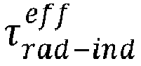
- ⁇ rad ⁇ ind eff can be measured or if a measured value is not available it can be used as a fitting parameter (see further).
- B is the Auger rate constant which can be measured or of which a value or at least an applicable range can be taken from literature for each 2D-semiconductor material. In the last case, B can be used as a fitting parameter within said range (see further).
- N is the carrier concentration (in cm -2 ), n d the trap density in the band gap (in cm -2 ) and F d the defect occupancy state.
- F d is related to the Fermi level of the material, and obtainable from literature.
- the variables a and b are correction terms which account for experimental uncertainties. The terms a and b can be set to zero or used as fitting parameters if the zero value of a and b does not allow to fit the experimental data to the theoretical model. The ' ⁇ ' symbol indicates 'is proportional to'.
- the method of the invention is performed on a sample comprising a support substrate carrying on its surface a layer of a 2D semiconductor material produced thereon, the layer exhibiting both direct and indirect bandgaps.
- the layer may for example be a TMDC 2-D semiconductor material, such as MOS 2 or WS 2 , with thickness greater than two monolayers.
- the layer is then illuminated by a light beam configured to generate a plurality of excitons. This is preferably a laser beam directed to a spot of the layer.
- the spot may have a diameter in the order of micrometres, for example about 1 ⁇ m.
- a laser beam with a wavelength of 532 nm is suitable.
- Photons emitted from the spot are detected by a detector configured to obtain the photoluminescence spectrum of the illuminated spot, i.e. the number of the detected photons as a function of their energy. This measurement may be performed using laser and detector tools which are known as such in the prior art for performing photoluminescence measurements.
- the carrier concentration is modulated by incrementally changing the output power of the laser within a given range.
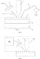
- a conceptual view of the required measurement setup is shown in Figure 1 .
- a laser 1 is oriented perpendicularly to a sample (other angles of the laser are also possible however), which comprises the base substrate 2 carrying a layer 3 of the 2D semiconductor material under investigation.
- a detector 4 is mounted laterally with respect to the laser, and is configured to detect photons 5 emitted from the irradiated surface of the layer 3.
- Figure 2 shows the spectra measured on a WS 2 flake having a surface of a few square micrometers, present on a SiO 2 substrate.
- the flake has a uniform thickness of 5 nm, i.e. the flake consists of several monolayers of WS 2 .
- the spectra labelled 6, 7 and 8 are respectively related to measurements obtained at 1%, 10% and 25% of the maximum available laser power of 1.34MW/cm 2 using a 532 nm wavelength laser beam of 1 ⁇ m in diameter.
- the image shows that the indirect peak, at about 1.55eV, significantly reduces when the laser power increases. This is caused by an increase in non-radiative defect-assisted Auger recombination as the photogenerated carrier concentration increases.
- the indirect peak is more sensitive to nonradiative recombination, explaining the experimental observations.
- the direct peak remains the same in amplitude but shifts along the X-axis in the range of 1.85 to 2 eV, likely from a combination of heating-induced strain and a small degree of local oxidation.
- FIG. 3 A similar set of spectra is illustrated in Figure 3 , measured on MoS 2 .
- the spectra 10 through 13 corresponding respectively to 0.1%, 1%, 10% and 25% of the maximum laser power.
- Photoluminescence (PL) spectra were collected in a confocal Raman microscopic system, using exciting lasers with primary wavelength of 532 nm (green). The laser radiation is focused onto the 2D material using a 100x objective lens with a spot-size around 1 ⁇ m. Photoluminescence spectra were resolved by a spectrometer using gratings of 600 mm-1 and acquired by a CCD (charge-coupled device) detector. Measurements were performed at room temperature, in air.
- CCD charge-coupled device
- N P laser 1 ⁇ R ⁇ A spot hv ⁇ ⁇ carrier
- P laser is the laser power (in W/cm 2 )
- a spot is the excitation area (in cm 2 )
- hv the excitation photon energy (in J)
- R the Fresnel reflection coefficient and a the absorption coefficient of the 2D material.
- R and a are known from literature.
- carrier is the carrier lifetime (in s), which can be measured using known techniques, such as time resolved photoluminescence, or a value or at least an applicable range can be found in literature. In the latter case, ⁇ carrier can be used as a fitting parameter.
- Figure 4 shows a number of curves which reflect the theoretical relation (1) for WS 2 and for different values of the trap density, ranging from 1 x 10 10 cm -2 for the upper curve 14 to 1 x 10 13 cm -2 for the lower curve 15.
- superimposed on these curves are the measured values of the ratio I ind /I dir as a function of the carrier concentration, taking into account the relation (2), and measured on two similar WS 2 flakes, as indicated by the two different symbols ' ⁇ ' and ' ⁇ '.
- the correction factors a and b were set to zero.
- the lifetime of the indirect transition ⁇ rad ⁇ ind eff is treated as a fitting parameter, since a precise determination of this value is yet unavailable for WS 2 and MoS 2 . All other parameters were determined from literature.
- the fitting process involved searching for the value of ⁇ rad ⁇ ind eff for which the measured data correspond as close as possible to one of the theoretical curves, within reasonable bounds. For the data points measured on WS 2 , it was found that when ⁇ rad ⁇ ind eff is 1 nanosecond, the measured data fit to the theoretical curve 16 corresponding to a trap density of 4.6 x 10 10 cm -2 . This illustrates how the trap density can be obtained by the method of the invention.
- the example of the measured data points obtained on WS 2 and shown in Figure 4 was successful for obtaining the trap density using only ⁇ rad ⁇ ind eff as a fitting parameter, while all the other parameters were either measured or taken from literature, and with correction terms a and b set to zero.
- the method is applicable also when additional parameters are not known or only known within a given range. For example, if measured values of B and ⁇ carrier are not available, nor good estimates of the correction terms a and b, the method may use a fitting algorithm that starts from estimated values for the unknown parameters, possibly lying within predetermined ranges obtained from literature. The fitting process is then performed by iterative steps until a closest match is found between the measured data and the theoretical model, yielding the trap density.
- Such algorithms are known as such in the art.
- the carrier concentration is modulated by using a constant laser power, and applying a variable back bias voltage to the substrate onto which the 2D semiconductor material is present.
- a conceptual view of the required measurement setup is shown in Figure 5 .
- the 2D material 3 is deposited on a dielectric material 20, which is itself deposited on an electrically conductive substrate 21, such as a metal or a highly doped semiconductor.
- the conductive substrate 21 may be grounded, and the bias voltage may be applied by contacting the 2D material 3 with a probe needle 22 placed at the bias voltage level V relative to the conductive substrate 21.
- the relation between the bias voltage and the carrier concentration is known from literature, for example from the document " Carrier statistics and quantum capacitance effects on mobility extraction in two-dimensional crystal semiconductor field-effect transistors", Nan Ma and Debdeep Jena, 2D Materials, Volume 2, 2015 .
- This paper takes into account the influence of the quantum capacitance of the dielectric layer 20, which is however only necessary in the case of very thin dielectric layers. In practice however, the method according to this embodiment does not require such thin layers. A thicker layer 20 can thus be used wherein the quantum capacitance is negligable.
- the carrier concentration can be calculated as the product of the applied bias voltage and the capacitance of the dielectric layer 20.
- the laser 1 and detector 4 are the same as in the setup shown in Figure 1 . By measuring the PL spectrum at different levels of the bias voltage, the measured relation between the ratio I ind /I dir can thus also be determined, and the above-described fitting process yields the value of the trap density.
- the equation (1) is valid also for other TMDC 2D-semiconductor materials besides WS 2 .
- the invention is however not limited to these materials nor to the equation (1) for describing the theoretical model.
- the balance between the different recombination mechanisms may require a different theoretical model to be developed.
- the method of the invention is applicable also in combination with such alternative models.
- the method of the invention may be used in-situ or in-line.
- In situ refers to the measurement of the trap density in the same tool as the one used for producing the 2D semiconductor material on its support substrate.
- In-line refers to the integration of the method into a semiconductor production process. The latter application is particularly useful as the method of the invention is non-invasive and may be executed quickly without slowing down or disrupting a production line.
- the method of the invention does not require the fabrication of a test device, and thereby avoids material defects induced by such device fabrication.
- the invention is equally related to an apparatus configured to perform the method of the invention.
- Such an apparatus may be devised for measurements in-situ or for measurements in-line, and the precise details of the apparatus may be slightly different according to these conditions.
- the basic components of any apparatus according to the invention are the following :
- the processing and calculation unit 101 may be a computer programmed to determine the measured relation between I ind /I dir and the carrier concentration and further comprising the theoretical relation, for example equation (1) and an algorithm for performing the fitting process and the determination of the trap density.
- the invention is also related to a computer program configured to perform the above three steps, when the program is run on the processing and calculation unit 101.
Landscapes
- Health & Medical Sciences (AREA)
- Biochemistry (AREA)
- Physics & Mathematics (AREA)
- Life Sciences & Earth Sciences (AREA)
- Chemical & Material Sciences (AREA)
- Analytical Chemistry (AREA)
- General Health & Medical Sciences (AREA)
- General Physics & Mathematics (AREA)
- Immunology (AREA)
- Pathology (AREA)
- Nuclear Medicine, Radiotherapy & Molecular Imaging (AREA)
- Testing Or Measuring Of Semiconductors Or The Like (AREA)
- Investigating, Analyzing Materials By Fluorescence Or Luminescence (AREA)
Abstract
Description
- The present invention is related to the characterization of 2-dimensional semiconductor materials, and in particular to a non-invasive technique that enables the determination of the trap density of these materials.
- Two-dimensional materials such as graphene and TMDC materials (transition metal dichalcogenide), have been under intense study for the past several years due to their unique mechanical and electrical properties. Of particular interest are the 2D semiconductor materials, i.e. 2D materials which exhibit a bandgap. The TMDC materials MoS2 and WS2 are examples of such 2D semiconductor materials. One of the factors that can strongly influence the performance of 2D semiconductor materials is the trap density which is dependent on intrinsic or contamination- related material properties of the 2D material, and on the substrate onto which the 2D layers are placed. Defects within the material or at the interface with the support substrate may generate electron or hole traps in the bandgap.
- For both graphene and TMDCs, it has been shown that traditional support substrates such as SiO2 can cause increased scattering, while enhanced performance is achieved when atomically flat 2D dielectrics, such as hexagonal boron nitride (hBN), are employed as support substrates. Performance, however, is often measured in terms of carrier mobility, which requires full device processing before the metric can be acquired. Device processing can however introduce non-idealities in the material which are difficult to deconvolute from electrical measurements.
- The use of photoluminescence-based techniques has been explored for studying the properties of the interface between 2D TDMC materials and different support substrates. The direct photoluminescence peak of one monolayer of MOS2, around 1.8eV, contains information on thickness, doping and strain. Also, direct exciton lifetime measurements can give insights on interface scattering.
- However, at this time there is no practical non-invasive technique that allows to measure the trap density in a 2D semiconductor material. Such a technique is crucial for the in-line measurements of the trap density in a semiconductor production process.
- The invention aims to provide a solution to the above-described problems. This aim is achieved by the method and apparatus according to the appended claims. According to the method of the invention, a spot on a layer of a 2D semiconductor material deposited on a support substrate is irradiated so as to generate excitons, so that photons are emitted from the layer. The photoluminescence spectrum is recorded and this is repeated for different values of the charge carrier concentration in the layer. The modulation of the charge carrier concentration may be realized by modulating the output power of the light source used to irradiate the sample, preferably a laser. The ratio is recorded between the photoluminescence intensity of a first peak in the spectrum related to radiative recombination from indirect bandgaps and the intensity of a second peak in the spectrum related to radiative recombination from direct bandgaps. More particularly, the relation is recorded between said ratio and the carrier concentration. This recorded relation is fitted to a theoretical model of the ratio that takes into account both recombination mechanisms, radiative and non-radiative. From this fitting process, the trap density within the bandgap is derived. The invention is equally related to an apparatus configured to perform the method of the invention.
- The invention is in particular related to a method for determining a trap density in a layer of a 2-dimensional semiconductor material, said layer exhibiting direct and indirect bandgaps between the valence band and the conduction band of the material, , the method comprising the steps of :
- providing a support substrate carrying on its surface said layer of 2D semiconductor material,
- illuminating a spot of the layer with a light beam, thereby generating electron-hole pairs,
- detecting emitted photons generated by direct and indirect bandgap transitions generated by radiative recombination of the electron-hole pairs, and determining a direct photoluminescence intensity Idir and an indirect photoluminescence intensity Iind,
- repeating the two preceding steps at different values of the charge carrier concentration in the layer by modulating the charge carrier concentration, to thereby obtain a measured relation between the ratio Iind/Idir and the carrier concentration,
- fitting the measured relation to a theoretical relation that takes into account both radiative and non-radiative recombination mechanisms, said theoretical relation being also a function of the trap density,
- calculating the trap density from the theoretical relation that fits the measured relation.
- According to an embodiment, the carrier concentration is modulated by illuminating the spot with a laser and by modulating the output power of the laser.
- According to an embodiment, the layer of 2D semiconductor material is deposited on a dielectric layer that is itself deposited on an electrically conductive substrate, and wherein the carrier concentration is modulated by changing a bias voltage between the layer of 2D semiconductor material and the conductive substrate.
- According to an embodiment, the layer of 2D semiconductor material consists of at least two monolayers of a transition metal dichalcogenide material, hereafter abbreviated as a TMDC material. Said TMDC material may be MoS2 or WS2.
- According to an embodiment, the theoretical relation between the ratio Iind/Idir and the carrier concentration is the following :


- The invention is equally related to an apparatus for performing the method of the invention, the apparatus comprising :
- A light source,
- A photon detector,
- A processing and calculation unit coupled to the detector and configured to
- ∘ determine the ratio Iind/Idir at various carrier concentrations, thereby obtaining the measured relation between the ratio Iind/Idir and the carrier concentration
- ∘ fit the measured relation to the theoretical relation,
- ∘ derive from the fitting step a value of the trap density.
- According to an embodiment, the light source is a laser configured to produce a laser beam, the output power of which may be incremented within in a given range.
- According to an embodiment, the light source is a laser and the apparatus further comprises a voltage probe configured to apply a bias voltage to the layer of 2D semiconductor material.
- According to an embodiment, the apparatus is integrated in an apparatus for producing the layer of 2D semiconductor material on the support substrate.
- The invention is equally related to the use of the method of the invention, for performing in-line measurements of the trap density in a semiconductor processing line.
- The invention is equally related to the use of the apparatus of the invention, for performing in-line measurements of the trap density in a semiconductor processing line.
- The invention is equally related to a computer program product configured to run on a processing and calculation unit and execute the steps stated in appended
claim 7. -
-
Figure 1 illustrates the measurement setup required for performing the method of the invention according to a first embodiment. -
Figure 2 illustrates the influence of the carrier concentration on the indirect and direct transition peaks in the photoluminescence spectrum obtained by illuminating a spot on a flake of WS2 having a uniform thickness of 5 nm. -
Figure 3 illustrates the same effect on a layer of MOS2. -
Figure 4 illustrates how the values of the ratio Iind/Idir measured as a function of the carrier concentration may be fitted to a theoretical model. -
Figure 5 illustrates the measurement setup required for performing the method of the invention according to a second embodiment. -
Figure 6 shows a conceptual image of an apparatus according to an embodiment of the invention. - As stated above, the direct photoluminescence peak of TMDC semiconductor materials has been used for characterizing a monolayer of the material. However, when multilayer TMDC is considered, the material transitions from a direct bandgap material to an indirect bandgap material, i.e. the material exhibits both direct and indirect bandgap. The band gap is the energy gap between the valence band and the conduction band of the material. For a direct bandgap, the crystal momentum is the same at the maximum energy level of the valence band and at the minimum energy level of the conduction band, whereas for an indirect bandgap, there is a shift in the crystal momentum between the maximum energy of the valence band and the minimum level of the conduction band. This results in differences in terms of the dominant recombination mechanism occurring in the material.
- When light is irradiated on a 2D semiconductor material, electron-hole pairs - excitons - are generated by an electron being excited from the valence band to the conduction band, provided that the photon energy of the light source is in excess of the bandgap of the material. Once generated, the electron-hole pair can recombine again through 3 mechanisms: Radiative, Shockley-Read-Hall (SRH) or defect-assisted Auger recombination. Radiative recombination occurs through the emission of a photon, which is detectable and which contributes to a specific peak in the photoluminescence (hereafter abbreviated as PL) spectrum, hereafter referred to as the 'direct peak'. Non-radiative recombination, i.e. SRH or defect-assisted Auger recombination, occurs when the exciton combines with a defect-generated trap state.
- Radiative recombination is the dominant mechanism for direct bandgaps, even when the trap density is high, as only a photon is needed for the excitons to decay, but for indirect bandgaps, both photons and phonons are needed for radiative recombination, the phonons being required for compensating the difference in crystal momentum. Therefore, non-radiative recombination mechanisms become more important in the case of indirect bandgaps, and in the presence of a sufficiently high trap density. However, with low enough trap density, radiative recombination still occurs also for indirect bandgaps, leading to the appearance of an indirect peak in the PL spectrum, at a lower photon energy compared to the direct peak. The intensity of the indirect peak decreases when the trap density becomes higher. However, the indirect peak is also an inverse function of the carrier concentration in the material. The higher the number of charge carriers, the higher the number of carriers which can recombine with trap states, hence the lower the indirect peak.
- The method of the invention uses the above-described relations for determining the trap density through a series of PL measurements at different carrier concentrations, in a 2D semiconductor material that exhibits both direct and indirect bandgaps, like for example a WS2 or MOS2 layer thicker than 2 monolayers. The ratio of the PL intensity (i.e. the photon count) of the indirect peak, Iind, to the PL intensity of the direct peak, Idir, is recorded as a function of the carrier concentration. The relation between Iind/Idir and the carrier concentration is then fitted to a theoretical model of the interaction between the carrier concentration and the trap density, taking into account the different recombination mechanisms. According to this model, the inverse relation between the ratio Iind/Idir and the carrier concentration is different for each value of the trap density. So by fitting the measured relation to one of the theoretical relations, the trap density is obtained.
- It has been found in prior research that for TMDC 2D-semiconductor materials, the dominant non-radiative recombination mechanism is the defect-assisted Auger mechanism. Taking into account this knowledge, i.e. neglecting the influence of SRH recombination in favour of radiative and Auger recombination, the inventors have developed a theoretical model that links the ratio Iind/Idir to the carrier concentration and the trap density according to the following equation :


- The method of the invention is performed on a sample comprising a support substrate carrying on its surface a layer of a 2D semiconductor material produced thereon, the layer exhibiting both direct and indirect bandgaps. The layer may for example be a TMDC 2-D semiconductor material, such as MOS2 or WS2, with thickness greater than two monolayers. The layer is then illuminated by a light beam configured to generate a plurality of excitons. This is preferably a laser beam directed to a spot of the layer. The spot may have a diameter in the order of micrometres, for example about 1 µm. For MoS2 or WS2, a laser beam with a wavelength of 532 nm is suitable. Photons emitted from the spot are detected by a detector configured to obtain the photoluminescence spectrum of the illuminated spot, i.e. the number of the detected photons as a function of their energy. This measurement may be performed using laser and detector tools which are known as such in the prior art for performing photoluminescence measurements.
- According to a preferred embodiment, the carrier concentration is modulated by incrementally changing the output power of the laser within a given range. A conceptual view of the required measurement setup is shown in
Figure 1 . Alaser 1 is oriented perpendicularly to a sample (other angles of the laser are also possible however), which comprises thebase substrate 2 carrying alayer 3 of the 2D semiconductor material under investigation. Adetector 4 is mounted laterally with respect to the laser, and is configured to detectphotons 5 emitted from the irradiated surface of thelayer 3. -
Figure 2 shows the spectra measured on a WS2 flake having a surface of a few square micrometers, present on a SiO2 substrate. The flake has a uniform thickness of 5 nm, i.e. the flake consists of several monolayers of WS2. The spectra labelled 6, 7 and 8 are respectively related to measurements obtained at 1%, 10% and 25% of the maximum available laser power of 1.34MW/cm2 using a 532 nm wavelength laser beam of 1 µm in diameter. The image shows that the indirect peak, at about 1.55eV, significantly reduces when the laser power increases. This is caused by an increase in non-radiative defect-assisted Auger recombination as the photogenerated carrier concentration increases. Due to the momentum conservation requirement, the indirect peak is more sensitive to nonradiative recombination, explaining the experimental observations. The direct peak remains the same in amplitude but shifts along the X-axis in the range of 1.85 to 2 eV, likely from a combination of heating-induced strain and a small degree of local oxidation. - A similar set of spectra is illustrated in
Figure 3 , measured on MoS2. Thespectra 10 through 13 corresponding respectively to 0.1%, 1%, 10% and 25% of the maximum laser power. - The measurements illustrated in
figures 2 and3 were obtained under the following conditions. Photoluminescence (PL) spectra were collected in a confocal Raman microscopic system, using exciting lasers with primary wavelength of 532 nm (green). The laser radiation is focused onto the 2D material using a 100x objective lens with a spot-size around 1 µm. Photoluminescence spectra were resolved by a spectrometer using gratings of 600 mm-1 and acquired by a CCD (charge-coupled device) detector. Measurements were performed at room temperature, in air. - The laser power is correlated to the carrier density through the following equation :

-
Figure 4 shows a number of curves which reflect the theoretical relation (1) for WS2 and for different values of the trap density, ranging from 1 x 1010 cm-2 for theupper curve 14 to 1 x 1013 cm-2 for thelower curve 15. Superimposed on these curves are the measured values of the ratio Iind/Idir as a function of the carrier concentration, taking into account the relation (2), and measured on two similar WS2 flakes, as indicated by the two different symbols '▲' and '●'. The correction factors a and b were set to zero. The lifetime of the indirect transition


theoretical curve 16 corresponding to a trap density of 4.6 x 1010 cm-2. This illustrates how the trap density can be obtained by the method of the invention. - The example of the measured data points obtained on WS2 and shown in
Figure 4 was successful for obtaining the trap density using only
- According to another embodiment, the carrier concentration is modulated by using a constant laser power, and applying a variable back bias voltage to the substrate onto which the 2D semiconductor material is present. A conceptual view of the required measurement setup is shown in
Figure 5 . In this case, it is necessary that the2D material 3 is deposited on adielectric material 20, which is itself deposited on an electricallyconductive substrate 21, such as a metal or a highly doped semiconductor. Theconductive substrate 21 may be grounded, and the bias voltage may be applied by contacting the2D material 3 with aprobe needle 22 placed at the bias voltage level V relative to theconductive substrate 21. The relation between the bias voltage and the carrier concentration is known from literature, for example from the document "Carrier statistics and quantum capacitance effects on mobility extraction in two-dimensional crystal semiconductor field-effect transistors", Nan Ma and Debdeep Jena, 2D Materials, . This paper takes into account the influence of the quantum capacitance of thedielectric layer 20, which is however only necessary in the case of very thin dielectric layers. In practice however, the method according to this embodiment does not require such thin layers. Athicker layer 20 can thus be used wherein the quantum capacitance is negligable. In this case the carrier concentration can be calculated as the product of the applied bias voltage and the capacitance of thedielectric layer 20. Thelaser 1 anddetector 4 are the same as in the setup shown inFigure 1 . By measuring the PL spectrum at different levels of the bias voltage, the measured relation between the ratio Iind/Idir can thus also be determined, and the above-described fitting process yields the value of the trap density. - The equation (1) is valid also for other TMDC 2D-semiconductor materials besides WS2. The invention is however not limited to these materials nor to the equation (1) for describing the theoretical model. For other materials, the balance between the different recombination mechanisms may require a different theoretical model to be developed. The method of the invention is applicable also in combination with such alternative models.
- The method of the invention may be used in-situ or in-line. In situ refers to the measurement of the trap density in the same tool as the one used for producing the 2D semiconductor material on its support substrate. In-line refers to the integration of the method into a semiconductor production process. The latter application is particularly useful as the method of the invention is non-invasive and may be executed quickly without slowing down or disrupting a production line. The method of the invention does not require the fabrication of a test device, and thereby avoids material defects induced by such device fabrication.
- The invention is equally related to an apparatus configured to perform the method of the invention. Such an apparatus may be devised for measurements in-situ or for measurements in-line, and the precise details of the apparatus may be slightly different according to these conditions. However, and as illustrated in
Figure 6 for anapparatus 100 suitable for performing the method according to the embodiment ofFigure 1 , the basic components of any apparatus according to the invention are the following : - A
light source 1, - A
photon detector 4, - A processing and
calculation unit 101 coupled to thedetector 4 and configured to :- ∘ determine the ratio Iind/Idir at various carrier concentrations, thereby obtaining the measured relation between the ratio Iind/Idir and the carrier concentration,
- ∘ fit the measured relation to the theoretical relation,
- ∘ derive from the fitting step a value of the trap density.
- The processing and
calculation unit 101 may be a computer programmed to determine the measured relation between Iind/Idir and the carrier concentration and further comprising the theoretical relation, for example equation (1) and an algorithm for performing the fitting process and the determination of the trap density. The invention is also related to a computer program configured to perform the above three steps, when the program is run on the processing andcalculation unit 101. - While the invention has been illustrated and described in detail in the drawings and foregoing description, such illustration and description are to be considered illustrative or exemplary and not restrictive. Other variations to the disclosed embodiments can be understood and effected by those skilled in the art in practicing the claimed invention, from a study of the drawings, the disclosure and the appended claims. In the claims, the word "comprising" does not exclude other elements or steps, and the indefinite article "a" or "an" does not exclude a plurality. The mere fact that certain measures are recited in mutually different dependent claims does not indicate that a combination of these measures cannot be used to advantage. Any reference signs in the claims should not be construed as limiting the scope.
Claims (13)
- A method for determining a trap density in a layer of a 2-dimensional semiconductor material, said layer exhibiting direct and indirect bandgaps between the valence band and the conduction band of the material, , the method comprising the steps of :- providing a support substrate (2;20,21) carrying on its surface said layer (3) of 2D semiconductor material,- illuminating a spot of the layer (3) with a light beam, thereby generating electron-hole pairs,- detecting emitted photons (5) generated by direct and indirect bandgap transitions generated by radiative recombination of the electron-hole pairs, and determining a direct photoluminescence intensity Idir and an indirect photoluminescence intensity Iind,- repeating the two preceding steps at different values of the charge carrier concentration in the layer (3) by modulating the charge carrier concentration, to thereby obtain a measured relation between the ratio Iind/Idir and the carrier concentration,- fitting the measured relation to a theoretical relation that takes into account both radiative and non-radiative recombination mechanisms, said theoretical relation being also a function of the trap density,- calculating the trap density from the theoretical relation that fits the measured relation.
- The method according to claim 1, wherein the carrier concentration is modulated by illuminating the spot with a laser (1) and by modulating the output power of the laser.
- The method according to claim 1, wherein the layer of 2D semiconductor material (3) is deposited on a dielectric layer (20) that is itself deposited on an electrically conductive substrate (21), and wherein the carrier concentration is modulated by changing a bias voltage between the layer of 2D semiconductor material (3) and the conductive substrate (21).
- The method according to any one of the preceding claims, wherein the layer of 2D semiconductor material (3) consists of at least two monolayers of a transition metal dichalcogenide material, hereafter abbreviated as a TMDC material.
- The method according to claim 4, wherein said TMDC material is MOS2 or WS2.
- The method according to claim 4 or 5, wherein the theoretical relation between the ratio Iind/Idir and the carrier concentration is the following :


- An apparatus (100) for performing the method according to claim 1, the apparatus comprising :- A light source (1),- A photon detector (4),- A processing and calculation unit (101) coupled to the detector (4) and configured to∘ determine the ratio Iind/Idir at various carrier concentrations, thereby obtaining the measured relation between the ratio Iind/Idir and the carrier concentration∘ fit the measured relation to the theoretical relation,∘ derive from the fitting step a value of the trap density.
- The apparatus according to claim 7, wherein the light source is a laser (1) configured to produce a laser beam, the output power of which may be incremented within in a given range.
- The apparatus according to claim 7, wherein the light source is a laser and further comprising a voltage probe (22) configured to apply a bias voltage to the layer of 2D semiconductor material (3).
- The apparatus according to any one of claims 7 to 9, wherein the apparatus is integrated in an apparatus for producing the layer (3) of 2D semiconductor material on the support substrate (2).
- Use of the method according to any one of claims 1 to 6, for performing in-line measurements of the trap density in a semiconductor processing line.
- Use of the apparatus according to claim 7 to 9, for performing in-line measurements of the trap density in a semiconductor processing line.
- A computer program product configured to run on a processing and calculation unit (101) and execute the steps stated in claim 7.
Priority Applications (2)
| Application Number | Priority Date | Filing Date | Title |
|---|---|---|---|
| EP20175167.4A EP3913356B1 (en) | 2020-05-18 | 2020-05-18 | A method for measuring the trap density in a 2-dimensional semiconductor material |
| US17/323,115 US11898958B2 (en) | 2020-05-18 | 2021-05-18 | Method for measuring the trap density in a 2-dimensional semiconductor material |
Applications Claiming Priority (1)
| Application Number | Priority Date | Filing Date | Title |
|---|---|---|---|
| EP20175167.4A EP3913356B1 (en) | 2020-05-18 | 2020-05-18 | A method for measuring the trap density in a 2-dimensional semiconductor material |
Publications (2)
| Publication Number | Publication Date |
|---|---|
| EP3913356A1 true EP3913356A1 (en) | 2021-11-24 |
| EP3913356B1 EP3913356B1 (en) | 2025-01-22 |
Family
ID=70740492
Family Applications (1)
| Application Number | Title | Priority Date | Filing Date |
|---|---|---|---|
| EP20175167.4A Active EP3913356B1 (en) | 2020-05-18 | 2020-05-18 | A method for measuring the trap density in a 2-dimensional semiconductor material |
Country Status (2)
| Country | Link |
|---|---|
| US (1) | US11898958B2 (en) |
| EP (1) | EP3913356B1 (en) |
Family Cites Families (4)
| Publication number | Priority date | Publication date | Assignee | Title |
|---|---|---|---|---|
| US9601299B2 (en) * | 2012-08-03 | 2017-03-21 | Kla-Tencor Corporation | Photocathode including silicon substrate with boron layer |
| EP3344972B1 (en) * | 2015-09-03 | 2022-12-14 | California Institute of Technology | Optical systems and methods of characterizing high-k dielectrics |
| US11024447B2 (en) | 2016-11-21 | 2021-06-01 | The Government Of The United States Of America, As Represented By The Secretary Of The Navy | Two-dimensional materials integrated with multiferroic layers |
| US10734531B2 (en) * | 2017-06-22 | 2020-08-04 | The Penn State Research Foundation | Two-dimensional electrostrictive field effect transistor (2D-EFET) |
-
2020
- 2020-05-18 EP EP20175167.4A patent/EP3913356B1/en active Active
-
2021
- 2021-05-18 US US17/323,115 patent/US11898958B2/en active Active
Non-Patent Citations (6)
| Title |
|---|
| C. ROBERT ET AL: "Exciton radiative lifetime in transition metal dichalcogenide monolayers", PHYSICAL REVIEW B, vol. 93, no. 20, May 2016 (2016-05-01), XP055749215, ISSN: 2469-9950, DOI: 10.1103/PhysRevB.93.205423 * |
| HAINING WANG ET AL: "Surface Recombination Limited Lifetimes of Photoexcited Carriers in Few-Layer Transition Metal Dichalcogenide MoS 2", NANO LETTERS, vol. 15, no. 12, 6 November 2015 (2015-11-06), US, pages 8204 - 8210, XP055749001, ISSN: 1530-6984, DOI: 10.1021/acs.nanolett.5b03708 * |
| HAINING WANG ET AL: "Ultrafast Dynamics of Defect-Assisted Electron-Hole Recombination in Monolayer MoS 2", NANO LETTERS, vol. 15, no. 1, 31 December 2014 (2014-12-31), US, pages 339 - 345, XP055749004, ISSN: 1530-6984, DOI: 10.1021/nl503636c * |
| KATHLEEN M MCCREARY ET AL: "A- and B-Exciton Photoluminescence Intensity Ratio as a Measure of Sample Quality for Transition Metal Dichalcogenide Monolayers", ARXIV.ORG, CORNELL UNIVERSITY LIBRARY, 201 OLIN LIBRARY CORNELL UNIVERSITY ITHACA, NY 14853, 4 December 2018 (2018-12-04), XP080989010, DOI: 10.1063/1.5053699 * |
| NAN MADEBDEEP JENA: "Carrier statistics and quantum capacitance effects on mobility extraction in two-dimensional crystal semiconductor field-effect transistors", 2D MATERIALS, vol. 2, 2015 |
| YUANZHENG LI ET AL: "The Auger process in multilayer WSe 2 crystals", NANOSCALE, vol. 10, no. 37, 2018, United Kingdom, pages 17585 - 17592, XP055748520, ISSN: 2040-3364, DOI: 10.1039/C8NR02567C * |
Also Published As
| Publication number | Publication date |
|---|---|
| EP3913356B1 (en) | 2025-01-22 |
| US11898958B2 (en) | 2024-02-13 |
| US20210356399A1 (en) | 2021-11-18 |
Similar Documents
| Publication | Publication Date | Title |
|---|---|---|
| Batista et al. | Temperature dependence of carrier mobility in Si wafers measured by infrared photocarrier radiometry | |
| CN109765206B (en) | Methods for characterizing defects in two-dimensional materials and their applications | |
| US8912799B2 (en) | Accurate measurement of excess carrier lifetime using carrier decay method | |
| CN107091822B (en) | The device and its detection method of double light source activation luminescence generated by light detection semiconductor defects | |
| US20250003893A1 (en) | Method for monitoring influence of defects in few-layer two-dimensional material on exciton transport | |
| Mendis et al. | Nanometre-scale optical property fluctuations in Cu2ZnSnS4 revealed by low temperature cathodoluminescence | |
| CN115728250B (en) | Semiconductor carrier dynamics test instrument and test method | |
| US11898958B2 (en) | Method for measuring the trap density in a 2-dimensional semiconductor material | |
| Pawlak et al. | Quantitative thermal wave phase imaging of an IR semi-transparent GaAs wafer using IR lock-in thermography | |
| US9103659B1 (en) | Method and system for junction depth identification for ultra shallow junctions | |
| US7038768B2 (en) | Optical measuring method for semiconductor multiple layer structures and apparatus therefor | |
| Lei et al. | Accurate electronic transport characterization of B+ ion-implanted silicon wafers with self-normalized nonlinear photocarrier radiometry | |
| CN114235764A (en) | Quantitative imaging characterization method for surface recombination rate of semiconductor wafer current carrier | |
| Martinuzzi et al. | Scanning techniques applied to the characterisation of P and N type multicrystalline silicon | |
| US8911145B2 (en) | Method to measure the characteristics in an electrical component | |
| US20230282526A1 (en) | Method and device for measuring the thickness of thin films even on rough substrates | |
| Maliński | Investigations of the possibility of determination of thermal parameters of Si and SiGe samples based on the Photo Thermal Radiometry technique | |
| CN113740265A (en) | Detection method of element ratio of multi-element material AnBxC1-x | |
| JPS63312649A (en) | Simultaneously measuring method for impurity level and carrier life in semiconductor | |
| US20250116505A1 (en) | Layer thickness determination by four-wave-mixing spectroscopy | |
| Maliński et al. | Influence of the doping level of silicon on its optical and recombination parameters measured with the nondestructive photothermal radiometry method | |
| Diesinger et al. | In situ measurement of the optical absorption coefficient of porous silicon | |
| JPH11173988A (en) | Crystal defect evaluation method | |
| Garcia et al. | Photo‐Carrier‐Radiometry (PCR) Metrology for Semiconductor Manufacturing Inspection | |
| Mauser et al. | Probing nanoscale thermal transport with cathodoluminescence thermometry |
Legal Events
| Date | Code | Title | Description |
|---|---|---|---|
| PUAI | Public reference made under article 153(3) epc to a published international application that has entered the european phase |
Free format text: ORIGINAL CODE: 0009012 |
|
| STAA | Information on the status of an ep patent application or granted ep patent |
Free format text: STATUS: THE APPLICATION HAS BEEN PUBLISHED |
|
| AK | Designated contracting states |
Kind code of ref document: A1 Designated state(s): AL AT BE BG CH CY CZ DE DK EE ES FI FR GB GR HR HU IE IS IT LI LT LU LV MC MK MT NL NO PL PT RO RS SE SI SK SM TR |
|
| B565 | Issuance of search results under rule 164(2) epc |
Effective date: 20201120 |
|
| STAA | Information on the status of an ep patent application or granted ep patent |
Free format text: STATUS: REQUEST FOR EXAMINATION WAS MADE |
|
| 17P | Request for examination filed |
Effective date: 20220520 |
|
| RBV | Designated contracting states (corrected) |
Designated state(s): AL AT BE BG CH CY CZ DE DK EE ES FI FR GB GR HR HU IE IS IT LI LT LU LV MC MK MT NL NO PL PT RO RS SE SI SK SM TR |
|
| GRAP | Despatch of communication of intention to grant a patent |
Free format text: ORIGINAL CODE: EPIDOSNIGR1 |
|
| STAA | Information on the status of an ep patent application or granted ep patent |
Free format text: STATUS: GRANT OF PATENT IS INTENDED |
|
| INTG | Intention to grant announced |
Effective date: 20231213 |
|
| P01 | Opt-out of the competence of the unified patent court (upc) registered |
Effective date: 20240208 |
|
| GRAJ | Information related to disapproval of communication of intention to grant by the applicant or resumption of examination proceedings by the epo deleted |
Free format text: ORIGINAL CODE: EPIDOSDIGR1 |
|
| STAA | Information on the status of an ep patent application or granted ep patent |
Free format text: STATUS: REQUEST FOR EXAMINATION WAS MADE |
|
| INTC | Intention to grant announced (deleted) | ||
| GRAP | Despatch of communication of intention to grant a patent |
Free format text: ORIGINAL CODE: EPIDOSNIGR1 |
|
| STAA | Information on the status of an ep patent application or granted ep patent |
Free format text: STATUS: GRANT OF PATENT IS INTENDED |
|
| INTG | Intention to grant announced |
Effective date: 20240910 |
|
| GRAS | Grant fee paid |
Free format text: ORIGINAL CODE: EPIDOSNIGR3 |
|
| GRAA | (expected) grant |
Free format text: ORIGINAL CODE: 0009210 |
|
| STAA | Information on the status of an ep patent application or granted ep patent |
Free format text: STATUS: THE PATENT HAS BEEN GRANTED |
|
| AK | Designated contracting states |
Kind code of ref document: B1 Designated state(s): AL AT BE BG CH CY CZ DE DK EE ES FI FR GB GR HR HU IE IS IT LI LT LU LV MC MK MT NL NO PL PT RO RS SE SI SK SM TR |
|
| REG | Reference to a national code |
Ref country code: GB Ref legal event code: FG4D |
|
| REG | Reference to a national code |
Ref country code: CH Ref legal event code: EP |
|
| REG | Reference to a national code |
Ref country code: IE Ref legal event code: FG4D |
|
| REG | Reference to a national code |
Ref country code: DE Ref legal event code: R096 Ref document number: 602020045052 Country of ref document: DE |
|
| REG | Reference to a national code |
Ref country code: NL Ref legal event code: MP Effective date: 20250122 |
|
| PG25 | Lapsed in a contracting state [announced via postgrant information from national office to epo] |
Ref country code: NL Free format text: LAPSE BECAUSE OF FAILURE TO SUBMIT A TRANSLATION OF THE DESCRIPTION OR TO PAY THE FEE WITHIN THE PRESCRIBED TIME-LIMIT Effective date: 20250122 |
|
| PG25 | Lapsed in a contracting state [announced via postgrant information from national office to epo] |
Ref country code: RS Free format text: LAPSE BECAUSE OF FAILURE TO SUBMIT A TRANSLATION OF THE DESCRIPTION OR TO PAY THE FEE WITHIN THE PRESCRIBED TIME-LIMIT Effective date: 20250422 |
|
| PG25 | Lapsed in a contracting state [announced via postgrant information from national office to epo] |
Ref country code: FI Free format text: LAPSE BECAUSE OF FAILURE TO SUBMIT A TRANSLATION OF THE DESCRIPTION OR TO PAY THE FEE WITHIN THE PRESCRIBED TIME-LIMIT Effective date: 20250122 |
|
| PG25 | Lapsed in a contracting state [announced via postgrant information from national office to epo] |
Ref country code: PL Free format text: LAPSE BECAUSE OF FAILURE TO SUBMIT A TRANSLATION OF THE DESCRIPTION OR TO PAY THE FEE WITHIN THE PRESCRIBED TIME-LIMIT Effective date: 20250122 |
|
| PG25 | Lapsed in a contracting state [announced via postgrant information from national office to epo] |
Ref country code: ES Free format text: LAPSE BECAUSE OF FAILURE TO SUBMIT A TRANSLATION OF THE DESCRIPTION OR TO PAY THE FEE WITHIN THE PRESCRIBED TIME-LIMIT Effective date: 20250122 |
|
| REG | Reference to a national code |
Ref country code: LT Ref legal event code: MG9D |
|
| PG25 | Lapsed in a contracting state [announced via postgrant information from national office to epo] |
Ref country code: NO Free format text: LAPSE BECAUSE OF FAILURE TO SUBMIT A TRANSLATION OF THE DESCRIPTION OR TO PAY THE FEE WITHIN THE PRESCRIBED TIME-LIMIT Effective date: 20250422 Ref country code: IS Free format text: LAPSE BECAUSE OF FAILURE TO SUBMIT A TRANSLATION OF THE DESCRIPTION OR TO PAY THE FEE WITHIN THE PRESCRIBED TIME-LIMIT Effective date: 20250522 |
|
| REG | Reference to a national code |
Ref country code: AT Ref legal event code: MK05 Ref document number: 1761801 Country of ref document: AT Kind code of ref document: T Effective date: 20250122 |
|
| PG25 | Lapsed in a contracting state [announced via postgrant information from national office to epo] |
Ref country code: HR Free format text: LAPSE BECAUSE OF FAILURE TO SUBMIT A TRANSLATION OF THE DESCRIPTION OR TO PAY THE FEE WITHIN THE PRESCRIBED TIME-LIMIT Effective date: 20250122 |
|
| PG25 | Lapsed in a contracting state [announced via postgrant information from national office to epo] |
Ref country code: PT Free format text: LAPSE BECAUSE OF FAILURE TO SUBMIT A TRANSLATION OF THE DESCRIPTION OR TO PAY THE FEE WITHIN THE PRESCRIBED TIME-LIMIT Effective date: 20250522 Ref country code: LV Free format text: LAPSE BECAUSE OF FAILURE TO SUBMIT A TRANSLATION OF THE DESCRIPTION OR TO PAY THE FEE WITHIN THE PRESCRIBED TIME-LIMIT Effective date: 20250122 |
|
| PG25 | Lapsed in a contracting state [announced via postgrant information from national office to epo] |
Ref country code: BG Free format text: LAPSE BECAUSE OF FAILURE TO SUBMIT A TRANSLATION OF THE DESCRIPTION OR TO PAY THE FEE WITHIN THE PRESCRIBED TIME-LIMIT Effective date: 20250122 Ref country code: GR Free format text: LAPSE BECAUSE OF FAILURE TO SUBMIT A TRANSLATION OF THE DESCRIPTION OR TO PAY THE FEE WITHIN THE PRESCRIBED TIME-LIMIT Effective date: 20250423 |
|
| PG25 | Lapsed in a contracting state [announced via postgrant information from national office to epo] |
Ref country code: AT Free format text: LAPSE BECAUSE OF FAILURE TO SUBMIT A TRANSLATION OF THE DESCRIPTION OR TO PAY THE FEE WITHIN THE PRESCRIBED TIME-LIMIT Effective date: 20250122 |
|
| PG25 | Lapsed in a contracting state [announced via postgrant information from national office to epo] |
Ref country code: SE Free format text: LAPSE BECAUSE OF FAILURE TO SUBMIT A TRANSLATION OF THE DESCRIPTION OR TO PAY THE FEE WITHIN THE PRESCRIBED TIME-LIMIT Effective date: 20250122 |
|
| PG25 | Lapsed in a contracting state [announced via postgrant information from national office to epo] |
Ref country code: SM Free format text: LAPSE BECAUSE OF FAILURE TO SUBMIT A TRANSLATION OF THE DESCRIPTION OR TO PAY THE FEE WITHIN THE PRESCRIBED TIME-LIMIT Effective date: 20250122 |
|
| PG25 | Lapsed in a contracting state [announced via postgrant information from national office to epo] |
Ref country code: DK Free format text: LAPSE BECAUSE OF FAILURE TO SUBMIT A TRANSLATION OF THE DESCRIPTION OR TO PAY THE FEE WITHIN THE PRESCRIBED TIME-LIMIT Effective date: 20250122 |
|
| PG25 | Lapsed in a contracting state [announced via postgrant information from national office to epo] |
Ref country code: IT Free format text: LAPSE BECAUSE OF FAILURE TO SUBMIT A TRANSLATION OF THE DESCRIPTION OR TO PAY THE FEE WITHIN THE PRESCRIBED TIME-LIMIT Effective date: 20250122 |
|
| PG25 | Lapsed in a contracting state [announced via postgrant information from national office to epo] |
Ref country code: EE Free format text: LAPSE BECAUSE OF FAILURE TO SUBMIT A TRANSLATION OF THE DESCRIPTION OR TO PAY THE FEE WITHIN THE PRESCRIBED TIME-LIMIT Effective date: 20250122 Ref country code: CZ Free format text: LAPSE BECAUSE OF FAILURE TO SUBMIT A TRANSLATION OF THE DESCRIPTION OR TO PAY THE FEE WITHIN THE PRESCRIBED TIME-LIMIT Effective date: 20250122 |
|
| REG | Reference to a national code |
Ref country code: DE Ref legal event code: R097 Ref document number: 602020045052 Country of ref document: DE |
|
| PG25 | Lapsed in a contracting state [announced via postgrant information from national office to epo] |
Ref country code: RO Free format text: LAPSE BECAUSE OF FAILURE TO SUBMIT A TRANSLATION OF THE DESCRIPTION OR TO PAY THE FEE WITHIN THE PRESCRIBED TIME-LIMIT Effective date: 20250122 |
|
| PG25 | Lapsed in a contracting state [announced via postgrant information from national office to epo] |
Ref country code: SK Free format text: LAPSE BECAUSE OF FAILURE TO SUBMIT A TRANSLATION OF THE DESCRIPTION OR TO PAY THE FEE WITHIN THE PRESCRIBED TIME-LIMIT Effective date: 20250122 |
|
| PLBE | No opposition filed within time limit |
Free format text: ORIGINAL CODE: 0009261 |
|
| STAA | Information on the status of an ep patent application or granted ep patent |
Free format text: STATUS: NO OPPOSITION FILED WITHIN TIME LIMIT |
|
| REG | Reference to a national code |
Ref country code: CH Ref legal event code: L10 Free format text: ST27 STATUS EVENT CODE: U-0-0-L10-L00 (AS PROVIDED BY THE NATIONAL OFFICE) Effective date: 20251203 |
|
| REG | Reference to a national code |
Ref country code: CH Ref legal event code: H13 Free format text: ST27 STATUS EVENT CODE: U-0-0-H10-H13 (AS PROVIDED BY THE NATIONAL OFFICE) Effective date: 20251223 |
|
| 26N | No opposition filed |
Effective date: 20251023 |
|
| PG25 | Lapsed in a contracting state [announced via postgrant information from national office to epo] |
Ref country code: LU Free format text: LAPSE BECAUSE OF NON-PAYMENT OF DUE FEES Effective date: 20250518 |
|
| PG25 | Lapsed in a contracting state [announced via postgrant information from national office to epo] |
Ref country code: CH Free format text: LAPSE BECAUSE OF NON-PAYMENT OF DUE FEES Effective date: 20250531 |
|
| GBPC | Gb: european patent ceased through non-payment of renewal fee |
Effective date: 20250518 |
|
| REG | Reference to a national code |
Ref country code: BE Ref legal event code: MM Effective date: 20250531 |
|
| PG25 | Lapsed in a contracting state [announced via postgrant information from national office to epo] |
Ref country code: MC Free format text: LAPSE BECAUSE OF FAILURE TO SUBMIT A TRANSLATION OF THE DESCRIPTION OR TO PAY THE FEE WITHIN THE PRESCRIBED TIME-LIMIT Effective date: 20250122 |
|
| PG25 | Lapsed in a contracting state [announced via postgrant information from national office to epo] |
Ref country code: GB Free format text: LAPSE BECAUSE OF NON-PAYMENT OF DUE FEES Effective date: 20250518 |
|
| PG25 | Lapsed in a contracting state [announced via postgrant information from national office to epo] |
Ref country code: IE Free format text: LAPSE BECAUSE OF NON-PAYMENT OF DUE FEES Effective date: 20250518 |
|
| PG25 | Lapsed in a contracting state [announced via postgrant information from national office to epo] |
Ref country code: BE Free format text: LAPSE BECAUSE OF NON-PAYMENT OF DUE FEES Effective date: 20250531 |
|
| PG25 | Lapsed in a contracting state [announced via postgrant information from national office to epo] |
Ref country code: FR Free format text: LAPSE BECAUSE OF NON-PAYMENT OF DUE FEES Effective date: 20250531 |
|
| PG25 | Lapsed in a contracting state [announced via postgrant information from national office to epo] |
Ref country code: LT Free format text: LAPSE BECAUSE OF FAILURE TO SUBMIT A TRANSLATION OF THE DESCRIPTION OR TO PAY THE FEE WITHIN THE PRESCRIBED TIME-LIMIT Effective date: 20250122 |
|
| PGFP | Annual fee paid to national office [announced via postgrant information from national office to epo] |
Ref country code: DE Payment date: 20260421 Year of fee payment: 7 |
|
| PG25 | Lapsed in a contracting state [announced via postgrant information from national office to epo] |
Ref country code: CY Free format text: LAPSE BECAUSE OF FAILURE TO SUBMIT A TRANSLATION OF THE DESCRIPTION OR TO PAY THE FEE WITHIN THE PRESCRIBED TIME-LIMIT Effective date: 20250122 |