US7038768B2 - Optical measuring method for semiconductor multiple layer structures and apparatus therefor - Google Patents
Optical measuring method for semiconductor multiple layer structures and apparatus therefor Download PDFInfo
- Publication number
- US7038768B2 US7038768B2 US10/642,184 US64218403A US7038768B2 US 7038768 B2 US7038768 B2 US 7038768B2 US 64218403 A US64218403 A US 64218403A US 7038768 B2 US7038768 B2 US 7038768B2
- Authority
- US
- United States
- Prior art keywords
- light
- sample
- spectrometer
- measurement
- detector
- Prior art date
- Legal status (The legal status is an assumption and is not a legal conclusion. Google has not performed a legal analysis and makes no representation as to the accuracy of the status listed.)
- Active, expires
Links
- 239000004065 semiconductor Substances 0.000 title claims abstract description 28
- 238000000034 method Methods 0.000 title claims description 17
- 230000003287 optical effect Effects 0.000 title description 12
- 239000000523 sample Substances 0.000 claims abstract description 62
- 238000001228 spectrum Methods 0.000 claims abstract description 36
- 238000005259 measurement Methods 0.000 claims abstract description 29
- 238000000103 photoluminescence spectrum Methods 0.000 claims abstract description 25
- 230000005684 electric field Effects 0.000 claims description 29
- 230000010355 oscillation Effects 0.000 claims description 25
- 230000005284 excitation Effects 0.000 claims description 11
- 238000005424 photoluminescence Methods 0.000 claims description 8
- 230000001678 irradiating effect Effects 0.000 claims description 5
- 230000000737 periodic effect Effects 0.000 claims 1
- 238000011156 evaluation Methods 0.000 description 9
- 230000008859 change Effects 0.000 description 7
- 238000005086 pumping Methods 0.000 description 6
- 238000004611 spectroscopical analysis Methods 0.000 description 6
- 238000012545 processing Methods 0.000 description 4
- 238000004364 calculation method Methods 0.000 description 3
- 238000001514 detection method Methods 0.000 description 3
- 238000010586 diagram Methods 0.000 description 3
- 239000000203 mixture Substances 0.000 description 3
- 238000003908 quality control method Methods 0.000 description 3
- 238000013441 quality evaluation Methods 0.000 description 3
- 229910001218 Gallium arsenide Inorganic materials 0.000 description 2
- 230000008901 benefit Effects 0.000 description 2
- 238000012986 modification Methods 0.000 description 2
- 230000004048 modification Effects 0.000 description 2
- 230000010287 polarization Effects 0.000 description 2
- 238000004458 analytical method Methods 0.000 description 1
- 230000004888 barrier function Effects 0.000 description 1
- 239000000969 carrier Substances 0.000 description 1
- 239000013078 crystal Substances 0.000 description 1
- 230000002950 deficient Effects 0.000 description 1
- 230000000694 effects Effects 0.000 description 1
- 238000000572 ellipsometry Methods 0.000 description 1
- 238000005516 engineering process Methods 0.000 description 1
- 238000004519 manufacturing process Methods 0.000 description 1
- 238000000691 measurement method Methods 0.000 description 1
- 230000007935 neutral effect Effects 0.000 description 1
- 230000003534 oscillatory effect Effects 0.000 description 1
- 238000000628 photoluminescence spectroscopy Methods 0.000 description 1
- 230000008569 process Effects 0.000 description 1
- 238000001055 reflectance spectroscopy Methods 0.000 description 1
- 239000007787 solid Substances 0.000 description 1
- 239000003381 stabilizer Substances 0.000 description 1
- 238000010408 sweeping Methods 0.000 description 1
- 238000000411 transmission spectrum Methods 0.000 description 1
- 238000002834 transmittance Methods 0.000 description 1
Images


Classifications
-
- G—PHYSICS
- G01—MEASURING; TESTING
- G01J—MEASUREMENT OF INTENSITY, VELOCITY, SPECTRAL CONTENT, POLARISATION, PHASE OR PULSE CHARACTERISTICS OF INFRARED, VISIBLE OR ULTRAVIOLET LIGHT; COLORIMETRY; RADIATION PYROMETRY
- G01J3/00—Spectrometry; Spectrophotometry; Monochromators; Measuring colours
- G01J3/28—Investigating the spectrum
- G01J3/42—Absorption spectrometry; Double beam spectrometry; Flicker spectrometry; Reflection spectrometry
- G01J3/433—Modulation spectrometry; Derivative spectrometry
- G01J3/4338—Frequency modulated spectrometry
-
- G—PHYSICS
- G01—MEASURING; TESTING
- G01N—INVESTIGATING OR ANALYSING MATERIALS BY DETERMINING THEIR CHEMICAL OR PHYSICAL PROPERTIES
- G01N21/00—Investigating or analysing materials by the use of optical means, i.e. using sub-millimetre waves, infrared, visible or ultraviolet light
- G01N21/17—Systems in which incident light is modified in accordance with the properties of the material investigated
- G01N21/47—Scattering, i.e. diffuse reflection
-
- G—PHYSICS
- G01—MEASURING; TESTING
- G01N—INVESTIGATING OR ANALYSING MATERIALS BY DETERMINING THEIR CHEMICAL OR PHYSICAL PROPERTIES
- G01N21/00—Investigating or analysing materials by the use of optical means, i.e. using sub-millimetre waves, infrared, visible or ultraviolet light
- G01N21/62—Systems in which the material investigated is excited whereby it emits light or causes a change in wavelength of the incident light
- G01N21/63—Systems in which the material investigated is excited whereby it emits light or causes a change in wavelength of the incident light optically excited
- G01N21/64—Fluorescence; Phosphorescence
- G01N21/6489—Photoluminescence of semiconductors
-
- G—PHYSICS
- G01—MEASURING; TESTING
- G01J—MEASUREMENT OF INTENSITY, VELOCITY, SPECTRAL CONTENT, POLARISATION, PHASE OR PULSE CHARACTERISTICS OF INFRARED, VISIBLE OR ULTRAVIOLET LIGHT; COLORIMETRY; RADIATION PYROMETRY
- G01J1/00—Photometry, e.g. photographic exposure meter
- G01J1/42—Photometry, e.g. photographic exposure meter using electric radiation detectors
- G01J2001/4242—Modulated light, e.g. for synchronizing source and detector circuit
-
- G—PHYSICS
- G01—MEASURING; TESTING
- G01N—INVESTIGATING OR ANALYSING MATERIALS BY DETERMINING THEIR CHEMICAL OR PHYSICAL PROPERTIES
- G01N21/00—Investigating or analysing materials by the use of optical means, i.e. using sub-millimetre waves, infrared, visible or ultraviolet light
- G01N21/17—Systems in which incident light is modified in accordance with the properties of the material investigated
- G01N21/47—Scattering, i.e. diffuse reflection
- G01N2021/4735—Solid samples, e.g. paper, glass
Definitions
- the present invention relates to quality evaluation and control of semiconductor multiple layer structures.
- An epitaxial wafer having a multiple layer structure is used for fabricating semiconductor devices, and the quality evaluation and control therefor are necessary in order to decrease the number of defectives and to reduce the fabrication cost.
- Items assessed for quality on an epitaxial wafer include thicknesses and compositions of the multiple layers. The thickness is mainly measured with a technique such as infrared-ray or X-ray interference by using interference of electromagnetic waves, or. ellipsometry (polarization analysis) by using change in the degree of polarization between incident and reflecting lights.
- compositions of the layers in an epitaxial wafer are evaluated with band gap energies obtained by spectrum measurement of photoluminescence generated by irradiation of excitation light such as laser beams (for example, Masashi Ozaki, Semiconductor Evaluation Technique, Ch. 7 [in Japanese], ed. Takashi Katouda, Sangyo Tosho, Tokyo, 1989).
- the internal electric field strength known to depend on the doping concentration and the state at the surface/interface in an epitaxial wafer. Further, the internal electric field strength was recently reported to have a correlation with current gain in a heterojunction bipolar transistor. Therefore, the internal electric field strength is regarded as an important item in quality evaluation on an epitaxial wafer.
- the internal electric field strength can be measured with a technique called light modulated reflection spectroscopy or photoreflectance (hereinafter referred also to PR) spectroscopy.
- PR photoreflectance
- a change in reflectance, ⁇ R/R caused by irradiating a sample with external modulated light such as laser light, called pumping light, is measured with light called probe light (detection light).
- probe light detection light
- the change in reflectance, ⁇ R/R is recorded as a function of wavelength or photon energy of the probe light.
- the change in reflectance, ⁇ R/R exhibits an oscillatory profile called Franz-Keldysh oscillations (for example, refer to “Franz-Keldysh Oscillations in Modulation Spectroscopy”, H. Shen and M. Dutta, Journal of Applied Physics, vol. 78, pp. 2151–2176 (1995)).
- the period of the oscillation is determined by the internal electric field strength. Therefore, the internal electric field can be investigated by analyzing the period of the Franz-Keldysh oscillations.
- Japanese Patent laid open Publication 11-51856/1999 shows that the photoreflectance from a sample can be detected solely from the integrated intensity thereof, without a spectrometer.
- the above-mentioned three items, thickness, band gap energy and internal electric field, are measured with techniques different from each other in the evaluation of the quality of the epitaxial wafer. Therefore, much time and work are needed in order to measure all the three items. Further, the cost is high for providing apparatuses for the three measuring techniques. This leads to a barrier for strict quality control.
- An object of the invention is to simply evaluate internal electric field strength, thickness and band gap energy in a semiconductor multiple layer structure.
- a first light source in a measuring apparatus for a semiconductor multiple layer structure, generates light for exciting a sample of the semiconductor multiple layer film to measure photoluminescence spectra and generates external modulated light to the sample for measurement of reflection spectra.
- a second light source generates white light for probe light to measure the reflection spectra.
- a spectrometer disperses light from the sample for the measurement of the photoluminescence spectra or disperses light from the first light source to irradiate the sample for the measurement of the reflection spectra.
- a first detector for the measurement of the photoluminescence spectra detects light emitted from the spectrometer and converts it to an electrical signal
- a second detector for the measurement of the reflection spectra detects light reflected from the sample irradiated with the probe light dispersed by the spectrometer.
- a guide member guides the light from the spectrometer to the first detector or guides the white light from the second light source to the second detector.
- a controller makes the guide member guide the white light from the second light source to the first detector and acquire electric signals from the first detector for the measurement of the reflection spectra and makes the changer guide the light from the spectrometer to the second detector and acquire electric signals from the second detector for the measurement of the photoluminescence spectra.
- a sample of semiconductor multiple layer structure is irradiated with excitation light, and photoluminescence from the sample after transmitting a spectrometer is detected while the spectrometer is swept, and the detected light intensity is recorded as a function of photon energy.
- White light is entered to the spectrometer to irradiate the sample with monochromatic light emitted from the spectrometer, and the spectrometer is swept while the sample is irradiated with the external modulated light to detect reflection light from the sample, and the detected reflection spectra are recorded as a function of photon energy.
- An advantage of the present invention is that the internal electric field strength, the thickness and the band gap energy in a semiconductor multiple layer structure can be measured with one apparatus.
- Another advantage of the present invention is that the internal electric field strength, the thickness and the band gap energy in a semiconductor multiple layer structure can be measured nondestructively by measuring both photoreflectance and photoluminescence spectra of the semiconductor multiple layer structure.
- FIG. 1 is a diagram of reflecting light in a semiconductor multiple layer film consisting of N layers;
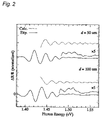
- FIG. 2 is a graph of Franz-Keldysh oscillations of a heterojunction structure of Al 0.3 Ga 0.7 As (thickness d nm)/GaAs;
- FIG. 3 is a diagram of an optical measurement system in a PL/PR measuring apparatus
- FIG. 4 is a diagram of a signal processing system in the PL/PR measuring apparatus
- FIG. 5 is a graph of a typical PL spectrum observed with the optical measuring system shown in FIG. 3 ;
- FIG. 6 is a graph of a typical PR spectrum observed with the optical measuring system shown in FIG. 3 ;
- FIG. 7 is a graph of the plot of the extremum positions of energy of Franz-Keldysh oscillations as a function of its index.
- the thickness, the band gap energy and the internal electric field in a semiconductor multiple layer structure prepared as an epitaxial wafer or the like were measured with different techniques. Then, it is desirable to measure them nondestructively, simultaneously, precisely and simply. In order to solve this problem, it would be necessary to develop a technique/principle for evaluating two or more quality items based on data obtained by one measuring technique and to provide an apparatus which can evaluate two or more items.
- the light modulated reflection (photoreflectance (PR)) spectroscopy used for the evaluation of the internal electric field and the photoluminescence (PL) spectroscopy used for evaluating the band gap energy are paid attention. They belong to technical field of spectroscopy and have common components for measurement. Therefore, it may be possible to provide a single apparatus for measuring light modulated reflection spectra or photoluminescence spectra, or PR and PL spectra may be measured by the single apparatus.
- PR photoreflectance
- PL photoluminescence
- the invention proposes a spectroscopic measurement method for the internal electric field strength and thickness on the basis of PR spectroscopy in order to achieve simple and simultaneous evaluation of the internal electric field strength, thickness and band gap energy in a semiconductor multiple layer structure in an epitaxial wafer.
- the internal electric field strength and the thickness are obtained simultaneously from Franz-Keldysh oscillations of the semiconductor multiple layer structure.
- a spectrum measuring apparatus is proposed to obtain both PR and PL spectra for precise evaluation based on the spectroscopic technologies.
- band gap energy obtained from PR spectra has no relative error to that obtained from PL spectra principally.
- the apparatus is very advantageous for precise evaluation of thickness based on PR spectra.
- FIG. 1 shows the reflected light from a semiconductor multiple layer structure consisting of N layers, where A 0 is incident light, and A n (n ⁇ 0) is light reflected from an interface between n-th layer L n and (n+1)-th layer L n+1 , where n is a natural number between 0 and N.
- the complex amplitude reflectance r of such a multiple layer structure is represented as follows.
- r 0 complex amplitude reflectance
- R 0 ⁇
- C n is a proportion constant related to transmittance.
- ⁇ n represents a quantity called as phase delay, given as follows.
- j is a natural number
- k j and d j are wave number of light and thickness of j-th layer in the multiple layer structure, respectively.
- ⁇ j is reflection angle at the j-th layer, and it can be calculated based on the incident angle to the sample and the known index of refraction of the sample.
- the energy reflectance R of the entire semiconductor multiple layer structure is given by a square
- the modulated reflectance ⁇ R n at interface L n /L n+1 between the n-th layer L n and the (n+1)-th layer L n +1 is represented as follows.
- ⁇ R n 2 r 0 (1 ⁇ R 0 ) C n Re[ ⁇ r n,n+1 e i ⁇ n ].
- Eq. (6) shows that the real and imaginary parts of the proportion constant B n in Eq. (4) correspond to Serafin coefficients ⁇ and ⁇ . In the visible light region, ⁇ is generally much larger than ⁇ . Therefore, B n can also be approximated as a real number. As a result, Eq. (4) is expressed as follows.
- ⁇ PR n 2 ik n ⁇ n ( ⁇ overscore (h) ⁇ ,F 0,n ) ⁇ W n (12)
- ⁇ (h ⁇ /2 ⁇ , F) is is represented as follows.
- g ⁇ ⁇ ( - ⁇ ) 1 4 ⁇ ⁇ - 1 ⁇ ⁇ sin ⁇ ( 4 3 ⁇ ⁇ 3 / 2 ) , ( 14 ⁇ a ) and f ⁇ ⁇ ( - ⁇ ) ⁇ - 1 4 ⁇ ⁇ - 1 ⁇ cos ⁇ ( 4 3 ⁇ ⁇ 3 / 2 ) . ( 14 ⁇ b ) It is assumed here that the effect of the life time of electrons/holes on the electro-optic function can be neglected.
- ⁇ R n (h ⁇ /2 ⁇ ) or Franz-Keldysh oscillations are represented as follows.
- FIG. 2 shows spectra (solid line) of Franz-Keldysh oscillations measured on a two-layer sample with Al 0.3 Ga 0.7 As (having thickness of d nm)/GaAs heterojunction structure and another spectra (dashed line) of Franz-Keldysh oscillations obtained with numerical calculation with Eq. (15).
- the Franz-Keldysh oscillations shown in FIG. 2 are normalized.
- “ ⁇ 5” means data displayed with a scale of five times on the axis of ordinates.
- phase delay is determined by performing this plot for the Franz-Keldysh oscillations arising from each interface.
- ⁇ n Eq. (2)
- a difference between ⁇ n and ⁇ n ⁇ 1 has a following relationship.
- ⁇ n ⁇ n ⁇ 1 2 k n d n cos ⁇ n .
- the thickness d n of n-th layer can be derived from this Equation.
- the internal electric field strength and the thickness in the layers of a semiconductor multiple layer structure can be evaluated at the same time from the Franz-Keldysh oscillations.
- the electric field strength can be obtained from the electro-optic energy by plotting the extrema of the Franz-Keldysh oscillations; however, the physical background on the intercept was not understood.
- the plot proposed here has a characteristic that the phase delay is obtained from the intercept at the axis of ordinates and that the thickness is obtained therefrom.
- FIGS. 3 and 4 show an apparatus to measure PR and PL spectra based on the above-mentioned principle.
- FIG. 3 schematically shows an optical measuring system
- FIG. 4 shows a signal processing system in the apparatus.
- PR and PL signals detected by the optical measuring system are processed.
- an optical path is changed with a mirror 14 in order to measure PR or PL spectra.
- the measurement data obtained by the optical measuring system is processed by the signal processing system shown in FIG. 4 .
- a light source 1 of white light is used to provide probe light, and it is, for example, a lamp.
- the mirror 14 reflects the light from the light source 1 toward a spectrometer 3 .
- a condenser lens 2 guides the light to the spectrometer 3 in order to generate the probe light.
- the spectrometer 3 generates monochromatic light from the lamp light and supplies the probe light to detect the reflectance R and modulated reflectance ⁇ R.
- the condenser lens 4 focuses the probe light generated by the spectrometer 3 onto the surface of a sample 5 .
- a light source 9 for excitation light such as a laser device, generates the external modulated light when PR spectra are measured.
- a power stabilizer 10 stabilizes the power of the light source 9 .
- a filter 11 for the light source such as a neutral density filter is provided for controlling the intensity of the excitation light.
- a modulator 12 such as an optical chopper converts the continuous wave form of the light to a square wave form.
- a condenser lens 13 focuses the external modulated light onto a region irradiated with the probe light in a surface of the sample.
- the excitation light source 9 such as a laser device generates the excitation light for PL spectrum measurement and/or the external modulated light for PR spectrum measurement.
- the spectrometer 3 generates the monochromatic light used as the probe light from the light emitted by the light source 1 in order to detect reflectance R and modulated reflectance ⁇ R. Further, the spectrometer 3 is used to disperse the light from a sample when PL spectra are measured.
- the condenser lens 6 guides the probe light reflected from the sample 5 to a detector 8 for PR measurement.
- a long path filter 7 removes the external modulated light scattered at the sample 5 .
- the detector 8 converts the light signals reflected from the sample 5 to electrical signals.
- the light source 9 When PL spectra are measured, the light source 9 generates excitation light for the sample 5 .
- the lens 4 condenses the light emitted from the sample 5 , as shown with dashed line, to the spectrometer 3 .
- the spectrometer 3 disperses the light emitted from the sample 5 , and the condenser lens 2 sends the photoluminescence to a detector 15 .
- the direction of the mirror 14 is changed so that the as-received photoluminescence is sent to the detector 15 .
- FIG. 4 schematically shows the signal processor for signals detected by the measuring system shown in FIG. 3 .
- a current-to-voltage converter 21 converts a current signal received from the detector 8 or 15 to a voltage signal.
- a band-path filter 22 is a frequency filter for separating the ac (corresponding to ⁇ R) and dc signals (signal R) from the overall signal.
- a dc voltmeter 23 is a device for measuring the dc component.
- a lock-in amplifier 24 is a device used for phase detection of the ac components or lock-in detection.
- a reference frequency signal for the lock-in amplifier 24 is provided from a modulator 12 of the optical measuring system.
- the signal from the detector 15 is measured by the lock-in amplifier, while when it is a continuous light, the signal is measured by the dc voltmeter 23 .
- a computer 25 controls the above-mentioned components for the measurement, acquires all the signals, and calculates on the basis of the acquired signals.
- the computer 25 controls the spectrometer 3 and records input signals from the dc voltmeter 23 or the lock-in amplifier 24 .
- the change in reflectance ⁇ R/R is calculated and recorded based on the signals from the detector 15 as a function of photon energy (h ⁇ /2 ⁇ ).
- the change in reflectance ⁇ R/R can be recorded as a function of photon energy (h ⁇ /2 ⁇ ).
- the internal electric field strength and the thickness are evaluated simultaneously based on the Franz-Keldysh oscillations.
- the excitation light such as laser light irradiates the sample 5 .
- the excitation light may be intermittent light generated by the modulator 12 or continuous light without using the modulator 12 .
- the combination of the modulator 12 and the lock-in amplifier 24 is used, where the lock-in amplifier 24 is used to detect the light in synchronization with the phase of the intermittent light.
- the phase of the lock-in amplifier is matched with that of the intermittent light as follows. First, the excitation light scattered by the sample 5 is collected by the condenser lens 4 to the spectrometer 3 . Then, the detector 15 detects the light transmitting the spectrometer 3 , and the phase of the lock-in amplifier 24 is matched with the detected signal.
- the signal obtained by the detector 15 is measured with the lock-in amplifier 24 when the pumping light is intermittent light, or with the dc voltmeter 23 when it is continuous light.
- the band gap energy is determined based on peaks of the observed photoluminescence spectra. The positions of the peaks correspond to band gap energy of each layer.
- the detected signal is transmitted through the band path filter 22 to separate the dc component corresponding to reflectance R from ac components corresponding to modulated reflectance ⁇ R.
- the computer 25 calculates ⁇ R/R to obtain PR signals.
- (Q) Numbering is performed on the extrema appearing in the Franz-Keldysh oscillations in the PR spectra, in the order from E 0 to higher energy, as shown in FIG. 6 .
Landscapes
- Physics & Mathematics (AREA)
- Spectroscopy & Molecular Physics (AREA)
- General Physics & Mathematics (AREA)
- Health & Medical Sciences (AREA)
- General Health & Medical Sciences (AREA)
- Chemical & Material Sciences (AREA)
- Analytical Chemistry (AREA)
- Biochemistry (AREA)
- Life Sciences & Earth Sciences (AREA)
- Immunology (AREA)
- Pathology (AREA)
- Nuclear Medicine, Radiotherapy & Molecular Imaging (AREA)
- Testing Or Measuring Of Semiconductors Or The Like (AREA)
- Length Measuring Devices By Optical Means (AREA)
- Investigating, Analyzing Materials By Fluorescence Or Luminescence (AREA)
- Investigating Or Analysing Materials By Optical Means (AREA)
Abstract
Description
where r0 is complex amplitude reflectance and R0 (≡|r0|2) is energy reflectance at the surface of the multiple layer structure, rn,n+1 is complex amplitude reflectance at Ln/Ln+1 interface, and Cn is a proportion constant related to transmittance. In Eq. (1), δn represents a quantity called as phase delay, given as follows.
where j is a natural number, and kj and dj are wave number of light and thickness of j-th layer in the multiple layer structure, respectively. Further, θj is reflection angle at the j-th layer, and it can be calculated based on the incident angle to the sample and the known index of refraction of the sample.
A relationship that |r|2=r·r* is used here where r* is a complex conjugate of r. Further, it is assumed that the complex amplitude reflectance at the surface of the multiple layer structure is sufficiently larger than those at the interfaces therein. In a visible light region, r0 can be taken generally as a real number. Then, the modulated reflectance ΔRn at interface Ln/Ln+1 between the n-th layer Ln and the (n+1)-th layer Ln +1 is represented as follows.
ΔR n=2r 0(1−R 0)C n Re[Δr n,n+1 e iδ
In Eq. (4), Δrn,n+1 is proportional to modulated component δ∈PR n+1 of dielectric function. That is,
Δr n,n+1 =B nδ∈PR n+1, (5)
where Bn is a proportion constant. In the case where δn→0, that is, for a bulk crystal having no overlayers except the surface, Eq. (4) follows Eq. (6) on PR signals derived by Serafin et al.
ΔR/R=αRe[δ∈ PR ]+βIm[δ∈ PR]. (6)
where ∈n(hω/2π, Fn) is a dielectric function perturbed by electric field Fn, where h is Planck constant, {overscore (h)} is h/2π and (hω/2π) represents photon energy. Fn on(z) and Fn off(z) are strengths of electric field under the irradiation of pumping light and under no irradiation, respectively, and they are given as follows.
where Wn is thickness of a depletion layer, ΔWn is change in Wn due to carriers generated by the irradiation of pumping light, and Fo,n represents electric field strength at the interface when not irradiated with the pumping light.
ΔW n /W n =ΔF n /F 0,n. (10)
If it is assumed that ΔEn<<F0,n and knΔWn<<1, Eq. (8a) is represented as follows.
where
Φn(z)≡e 2ik
Further, by approximating
Φn(z+ΔW n)−Φn(z)=(dΦ n(z)/dz)ΔW n,
and by neglecting terms higher than (ΔWn)2, δ∈PR n is represented as follows.
δ∈n PR({overscore (h)}ω)=2ik nΔ∈n({overscore (h)}ω,F 0,n)ΔW n (12)
In Eq. (13a), g(−η) and f(−η) are functions called as electro-optic functions, and asymptotic solutions thereof at higher energy region above the band gap energy are represented as follows.
It is assumed here that the effect of the life time of electrons/holes on the electro-optic function can be neglected.
where Eo,n+1 is band gap energy of (n+1)-th layer. Further, (h/2π)Θn+1 is a physical quantity called as electro-optic energy, and it is represented by a following Equation.
where e and μn+1 are elementary charge and reduced mass of electron and hole, respectively.
The plot of the extrema of the Franz-Keldysh oscillations according to Eq. (17) has a linear form. Then, the slope of the line gives the electro-optic energy (h/2π)Θn+1, and the electric field strength F0,n+1 can be calculated from this value based on Eq. (16). On the other hand, an intercept at the axis of ordinates gives phase delay δn. The phase delay is determined by performing this plot for the Franz-Keldysh oscillations arising from each interface. According to the definition of δn (Eq. (2)), a difference between δn and δn−1 has a following relationship.
δn−δn−1=2k n d n cos θn. (18)
Claims (5)
Applications Claiming Priority (2)
| Application Number | Priority Date | Filing Date | Title |
|---|---|---|---|
| JP2003-9515 | 2003-01-17 | ||
| JP2003009515A JP4031712B2 (en) | 2003-01-17 | 2003-01-17 | Spectroscopic measurement method and spectroscopic measurement apparatus for semiconductor multilayer film |
Publications (2)
| Publication Number | Publication Date |
|---|---|
| US20050099623A1 US20050099623A1 (en) | 2005-05-12 |
| US7038768B2 true US7038768B2 (en) | 2006-05-02 |
Family
ID=32898990
Family Applications (1)
| Application Number | Title | Priority Date | Filing Date |
|---|---|---|---|
| US10/642,184 Active 2024-07-19 US7038768B2 (en) | 2003-01-17 | 2003-08-18 | Optical measuring method for semiconductor multiple layer structures and apparatus therefor |
Country Status (2)
| Country | Link |
|---|---|
| US (1) | US7038768B2 (en) |
| JP (1) | JP4031712B2 (en) |
Cited By (2)
| Publication number | Priority date | Publication date | Assignee | Title |
|---|---|---|---|---|
| US20050274913A1 (en) * | 2004-06-14 | 2005-12-15 | Canon Kabushiki Kaisha | Object data input apparatus and object reconstruction apparatus |
| US9209096B2 (en) | 2010-07-30 | 2015-12-08 | First Solar, Inc | Photoluminescence measurement |
Families Citing this family (7)
| Publication number | Priority date | Publication date | Assignee | Title |
|---|---|---|---|---|
| JP4441381B2 (en) | 2004-10-29 | 2010-03-31 | 三菱電機株式会社 | Method for measuring surface carrier recombination velocity |
| JP4777003B2 (en) * | 2005-07-28 | 2011-09-21 | 三菱電機株式会社 | Semiconductor layer inspection method and apparatus |
| WO2007049259A1 (en) * | 2005-10-24 | 2007-05-03 | Optical Metrology Patents Limited | An optical measurement apparatus and method |
| JP5125252B2 (en) * | 2007-06-25 | 2013-01-23 | 三菱電機株式会社 | Nitride semiconductor evaluation method and evaluation apparatus |
| FR2956208B1 (en) * | 2010-02-05 | 2012-04-27 | Centre Nat Rech Scient | METHOD FOR NON-CONTACT DETERMINATION OF CHARACTERISTICS OF A PHOTOCONVERTER |
| JP2011180039A (en) * | 2010-03-02 | 2011-09-15 | Sigma Koki Kk | Specimen damage analyzer |
| KR101493838B1 (en) | 2013-11-26 | 2015-02-17 | 포항공과대학교 산학협력단 | Microscopy Scanning Photoluminescence. |
Citations (3)
| Publication number | Priority date | Publication date | Assignee | Title |
|---|---|---|---|---|
| US5064283A (en) * | 1989-09-14 | 1991-11-12 | The United States Of America As Represented By The Secretary Of The Army | Spectroscopy characterization module |
| JPH1151856A (en) | 1997-08-07 | 1999-02-26 | Nippon Telegr & Teleph Corp <Ntt> | Method for measuring photoreflectance mapping |
| JP2001110806A (en) | 1999-10-12 | 2001-04-20 | Matsushita Electric Ind Co Ltd | Manufacturing method of semiconductor device and manufacturing device of semiconductor device |
-
2003
- 2003-01-17 JP JP2003009515A patent/JP4031712B2/en not_active Expired - Fee Related
- 2003-08-18 US US10/642,184 patent/US7038768B2/en active Active
Patent Citations (3)
| Publication number | Priority date | Publication date | Assignee | Title |
|---|---|---|---|---|
| US5064283A (en) * | 1989-09-14 | 1991-11-12 | The United States Of America As Represented By The Secretary Of The Army | Spectroscopy characterization module |
| JPH1151856A (en) | 1997-08-07 | 1999-02-26 | Nippon Telegr & Teleph Corp <Ntt> | Method for measuring photoreflectance mapping |
| JP2001110806A (en) | 1999-10-12 | 2001-04-20 | Matsushita Electric Ind Co Ltd | Manufacturing method of semiconductor device and manufacturing device of semiconductor device |
Non-Patent Citations (2)
| Title |
|---|
| H. Shen et al., "Franz-Keldysh Oscillations In Modulation Spectroscopy", J. Appl. Phys., Aug. 1995, pp. 2151-2176, 78(4). |
| T. Katoda, "Techniques For Evaluating a Semiconductor", Textbook, 1989. |
Cited By (3)
| Publication number | Priority date | Publication date | Assignee | Title |
|---|---|---|---|---|
| US20050274913A1 (en) * | 2004-06-14 | 2005-12-15 | Canon Kabushiki Kaisha | Object data input apparatus and object reconstruction apparatus |
| US7189984B2 (en) * | 2004-06-14 | 2007-03-13 | Canon Kabushiki Kaisha | Object data input apparatus and object reconstruction apparatus |
| US9209096B2 (en) | 2010-07-30 | 2015-12-08 | First Solar, Inc | Photoluminescence measurement |
Also Published As
| Publication number | Publication date |
|---|---|
| US20050099623A1 (en) | 2005-05-12 |
| JP2004219371A (en) | 2004-08-05 |
| JP4031712B2 (en) | 2008-01-09 |
Similar Documents
| Publication | Publication Date | Title |
|---|---|---|
| US7400402B2 (en) | Modulated scatterometry | |
| US6320666B1 (en) | Apparatus for evaluating metalized layers on semiconductors | |
| US6268916B1 (en) | System for non-destructive measurement of samples | |
| US6665071B2 (en) | Method for determining ion concentration and energy of shallow junction implants | |
| US7362441B2 (en) | Modulated reflectance measurement system using UV probe | |
| JPH08335617A (en) | Method and equipment for response analysis of semiconductor material using optical stimulation | |
| KR20130114242A (en) | Device for detecting foreign matter and method for detecting foreign matter | |
| US6535285B1 (en) | Combination thermal wave and optical spectroscopy measurement system | |
| US7847937B1 (en) | Optical measurment systems and methods | |
| US7280215B2 (en) | Photothermal system with spectroscopic pump and probe | |
| US7038768B2 (en) | Optical measuring method for semiconductor multiple layer structures and apparatus therefor | |
| JPH03163842A (en) | Method for measuring interface characteristic of semiconductor material by light reflection method | |
| JP2001507127A (en) | In-situ observation of electronic properties by ellipsometry | |
| US6982791B2 (en) | Scatterometry to simultaneously measure critical dimensions and film properties | |
| US6952261B2 (en) | System for performing ellipsometry using an auxiliary pump beam to reduce effective measurement spot size | |
| Ghosh et al. | Photoreflectance spectroscopy with white light pump beam | |
| US20080074668A1 (en) | Modulated optical reflectance measurement system with enhanced sensitivity | |
| WO2003102557A1 (en) | Method of measuring electric characteristics of flat substrate using terahertz light | |
| RU2423684C2 (en) | Optical measurement method for material | |
| JPH01181434A (en) | Beam modulated spectroscope |
Legal Events
| Date | Code | Title | Description |
|---|---|---|---|
| AS | Assignment |
Owner name: MITSUBISHI DENKI KABUSHIKI KAISHA, JAPAN Free format text: ASSIGNMENT OF ASSIGNORS INTEREST;ASSIGNORS:TAKEUCHI, HIDEO;YAMAMOTO, YOSHITSUGU;REEL/FRAME:014407/0151 Effective date: 20030724 |
|
| FEPP | Fee payment procedure |
Free format text: PAYOR NUMBER ASSIGNED (ORIGINAL EVENT CODE: ASPN); ENTITY STATUS OF PATENT OWNER: LARGE ENTITY |
|
| STCF | Information on status: patent grant |
Free format text: PATENTED CASE |
|
| FPAY | Fee payment |
Year of fee payment: 4 |
|
| FPAY | Fee payment |
Year of fee payment: 8 |
|
| MAFP | Maintenance fee payment |
Free format text: PAYMENT OF MAINTENANCE FEE, 12TH YEAR, LARGE ENTITY (ORIGINAL EVENT CODE: M1553) Year of fee payment: 12 |