EP3909096B1 - Schutz vor elektromagnetischer störung für radome - Google Patents
Schutz vor elektromagnetischer störung für radome Download PDFInfo
- Publication number
- EP3909096B1 EP3909096B1 EP20700681.8A EP20700681A EP3909096B1 EP 3909096 B1 EP3909096 B1 EP 3909096B1 EP 20700681 A EP20700681 A EP 20700681A EP 3909096 B1 EP3909096 B1 EP 3909096B1
- Authority
- EP
- European Patent Office
- Prior art keywords
- coating
- frequency band
- substrate
- partly
- cover
- Prior art date
- Legal status (The legal status is an assumption and is not a legal conclusion. Google has not performed a legal analysis and makes no representation as to the accuracy of the status listed.)
- Active
Links
Images

Classifications
-
- H—ELECTRICITY
- H01—ELECTRIC ELEMENTS
- H01Q—ANTENNAS, i.e. RADIO AERIALS
- H01Q1/00—Details of, or arrangements associated with, antennas
- H01Q1/42—Housings not intimately mechanically associated with radiating elements, e.g. radome
-
- H—ELECTRICITY
- H01—ELECTRIC ELEMENTS
- H01Q—ANTENNAS, i.e. RADIO AERIALS
- H01Q1/00—Details of, or arrangements associated with, antennas
- H01Q1/42—Housings not intimately mechanically associated with radiating elements, e.g. radome
- H01Q1/422—Housings not intimately mechanically associated with radiating elements, e.g. radome comprising two or more layers of dielectric material
-
- H—ELECTRICITY
- H01—ELECTRIC ELEMENTS
- H01Q—ANTENNAS, i.e. RADIO AERIALS
- H01Q1/00—Details of, or arrangements associated with, antennas
- H01Q1/27—Adaptation for use in or on movable bodies
- H01Q1/32—Adaptation for use in or on road or rail vehicles
- H01Q1/3208—Adaptation for use in or on road or rail vehicles characterised by the application wherein the antenna is used
- H01Q1/3233—Adaptation for use in or on road or rail vehicles characterised by the application wherein the antenna is used particular used as part of a sensor or in a security system, e.g. for automotive radar, navigation systems
-
- H—ELECTRICITY
- H01—ELECTRIC ELEMENTS
- H01Q—ANTENNAS, i.e. RADIO AERIALS
- H01Q1/00—Details of, or arrangements associated with, antennas
- H01Q1/27—Adaptation for use in or on movable bodies
- H01Q1/32—Adaptation for use in or on road or rail vehicles
- H01Q1/325—Adaptation for use in or on road or rail vehicles characterised by the location of the antenna on the vehicle
- H01Q1/3283—Adaptation for use in or on road or rail vehicles characterised by the location of the antenna on the vehicle side-mounted antennas, e.g. bumper-mounted, door-mounted
-
- H—ELECTRICITY
- H01—ELECTRIC ELEMENTS
- H01Q—ANTENNAS, i.e. RADIO AERIALS
- H01Q1/00—Details of, or arrangements associated with, antennas
- H01Q1/42—Housings not intimately mechanically associated with radiating elements, e.g. radome
- H01Q1/425—Housings not intimately mechanically associated with radiating elements, e.g. radome comprising a metallic grid
-
- H—ELECTRICITY
- H01—ELECTRIC ELEMENTS
- H01Q—ANTENNAS, i.e. RADIO AERIALS
- H01Q15/00—Devices for reflection, refraction, diffraction or polarisation of waves radiated from an antenna, e.g. quasi-optical devices
- H01Q15/0006—Devices acting selectively as reflecting surface, as diffracting or as refracting device, e.g. frequency filtering or angular spatial filtering devices
- H01Q15/0013—Devices acting selectively as reflecting surface, as diffracting or as refracting device, e.g. frequency filtering or angular spatial filtering devices said selective devices working as frequency-selective reflecting surfaces, e.g. FSS, dichroic plates, surfaces being partly transmissive and reflective
Definitions
- the invention is directed to a cover for at least one antenna emitting and/or sensing electromagnetic radiation in at least one first frequency band, the cover comprising at least one first surface facing the antenna and at least one second surface averted to the antenna, wherein the cover comprises at least one substrate being transmissive for electromagnetic radiation and at least one first coating covering the substrate in at least one first area, the first coating being transmissive for electromagnetic radiation of at least the first frequency band.
- Such covers which are referred to as radomes in case the antenna is used to emit or receive radar waves, are generally known from the state of the art.
- US 6,518,936 B1 discloses a precision edged radome. It is proposed that the radome includes a patterned copper film functioning as a frequency selective surface.
- Such radomes are furthermore more and more used in the automotive industry.
- driver-assistance-systems there is a growth of electromagnetic wave emitting and/or receiving devices in vehicles driven by increased safety and vehicle autonomy requirements.
- Very often used sensors are radar systems using frequencies of 24 GHz or 77 GHz that are located at the front of the vehicle. These systems are used for control of various drive-assistance-systems such as autonomous cruise control.
- the antenna of such systems is located behind components of the vehicle in the front area of the car. Especially it is preferred to locate theses antennas in the area of the emblem of the vehicle, showing the name of the manufacturer or its trademark.
- a radome used on a vehicle has to fulfill the before described technical needs but on the other hand has to provide an aesthetic appearance.
- the later makes it necessary that the cover requires metallic finishes or metallic graphics to show the respective emblem. This however creates problems because the metal finishes that are required for the outer appearance and visual effects, attenuate a radar and prevent its proper function.
- radar units are typically 2 in 1 devices with both transmitter and receiver in the same element.
- Such systems can be located in the bumper area of the car but in most cases in which the radar units are used to control the emergency break assistant (EBA) and adaptive cruise control (ACC) it is preferred that the system sits behind the manufacturer emblem which hence acts as radome.
- EBA emergency break assistant
- ACC adaptive cruise control
- US 2018/015207 A1 describes radomes for vehicles, in particular a multi-piece vehicle radome having a non-uniform back piece.
- DE 10 2015 217 744 A1 describes a radome for a distance warning radar of a motor vehicle with a design element, for example a brand emblem, which is visible from the outside and is integrated in the radome.
- JP 2010 111010 A describes a cover for a wave radar having a resin layer and a base material layer respectively on both the surfaces of a decorated body, which is trimmed into a final external form, by injection molding.
- US 2012/119961 A1 describes a radome or cover for radar devices disposed behind the front grill of an automobile, wherein the radome or cover protects the radar device while presenting a decorative metallic image.
- US 2003/052810 A1 describes a device to conceal a radar for the transmission and reception of electromagnetic waves.
- US 2013/194687 A1 relates to a mirror formed on a plastic substrate, the mirror being for use primarily in automotive applications.
- the first coating is reflective for electromagnetic radiation falling onto the second surface and having a frequency within at least one second frequency band.
- the present invention provides a cover for at least one antenna emitting and/or sensing electromagnetic radiation in at least one first frequency band, being a radar frequency, the cover comprising at least one first surface configured to face the antenna and at least one second surface configured to be averted to the antenna, wherein the cover comprises at least one substrate being transmissive for electromagnetic radiation of the first frequency band and a second frequency band comprising visual light and at least one first coating covering the substrate in at least one first area, the first coating being transmissive for electromagnetic radiation of at least the first frequency band and being reflective for electromagnetic radiation falling onto the second surface and having a frequency within the second frequency band, wherein the first coating is configured to act as a frequency selective surface bandpass filter trimmed such that electromagnetic radiation of the first frequency band is transmitted, whereas radiation in the second frequency band is reflected, wherein the cover further comprises i) at least one covering layer located on a side of the first coating being located averted to the substrate, wherein the covering layer is transparent, at least semitransparent, for the second frequency band, or ii)
- the antenna is a radar antenna and/or the first frequency band is radar frequency, especially 10GHz to 130 GHz, preferably 20 GHz to 100 GHz, more preferred 20GHz to 30 GHz, 70GHz to 80GHz and/or 90GHz to 100GHz, most preferably 24 GHz, 77 GHz or 93GHz.
- the invention proposes that the substrate is transmissive for electromagnetic radiation in the first frequency band and/or in at least one third frequency band, wherein preferably the second frequency band is at least partly identical to the third frequency band.
- the first coating is located between the substrate and the antenna and/or located on the side of the first surface of the substrate.
- the first coating is located on the side of the second surface of the substrate.
- At least one stress controlling layer is located between the substrate and the first coating.
- An inventive cover can be characterized by at least one second coating, preferably at least partly located between the substrate and/or the first coating on the one hand and the antenna on the other hand, wherein the second coating is at least partly non transmissive and/or opaque in at least one fourth frequency band, preferably the second frequency band and/or the third frequency band, and/or transmissive in the first frequency band.
- a cover can be characterized by at least one masking layer at least partly covering the first coating and/or the substrate, wherein the making layer is at least partly non transmissive and/or opaque in at least one fifth frequency band, preferably the second frequency band, the third frequency band and/or the fourth frequency band, and/or transmissive in the first frequency band.
- the cover can be characterized in that, the second frequency band, the third frequency band and/or the fourth frequency band, comprises 384THz to 789THz and/or visual light.
- the second frequency band, the fourth frequency band and/or the fifth frequency band covers the area of 384THz to 789THz and/or the third frequency band covers only partly the area of 384THz to 789THz.
- the invention furthermore proposes that at least one covering layer is located on a side of the first coating being located averted to the substrate, wherein the covering layer is transparent, at least semitransparent for the second, third, fourth and/or fifth frequency band.
- the substrate comprises at least partly at least one thermoplastic material, preferably polycarbonate, polymethylmethacrylate, polyethylene, polyester, polyvinyl chloride, polypropylene, polystyrene, acrylonitrile butadiene styrene, acrylonitrile ethylene styrene, polyacrylate and/or a mixture thereof.
- thermoplastic material preferably polycarbonate, polymethylmethacrylate, polyethylene, polyester, polyvinyl chloride, polypropylene, polystyrene, acrylonitrile butadiene styrene, acrylonitrile ethylene styrene, polyacrylate and/or a mixture thereof.
- the first coating comprises at least one metallic material, preferably chrome, aluminium, silver, zinc, copper, nickel, vanadium, titanium, zirconium, niobium, gold, rhodium, cobalt, manganese, molybdenum, tantalum, silver and/or a mixture thereof.
- the first coating acts as a frequency selective surface bandpass filter and/or comprises at least one repetitive pattern, wherein the pattern preferably comprises, especially a plurality of elements being formed as, crosses, circles, squares, stars, rectangles, lines, hexagons, ellipsoids, polygons, annulus, semicircles, circular sectors, triquetra, lune, arbelos, spiral, lemniscates, triangles and/or oval forms.
- the elements are formed by, especially from each other separated, openings and/or gaps within the first coating.
- the elements are formed by, especially from each other separated and/or not interconnected, areas of the first coating.
- the second coating and/or the masking layer comprises at least one thermoplastic, preferably polycarbonate (PC), acrylonitrile butadiene styrene (ABS), acrylonitrile ethylene styrene (AES) and/or polycarbonate acrylonitrile butadiene styrene (PCABS).
- PC polycarbonate
- ABS acrylonitrile butadiene styrene
- AES acrylonitrile ethylene styrene
- PCABS polycarbonate acrylonitrile butadiene styrene
- the invention can be further characterized in that the first coating, when viewed onto the second surface of the cover presents at least one logo, character, number, graphical trademark, trademark, decorative design and/or decorative pattern.
- the masking layer covers the first coating such that when viewed onto the second surface, only at least a first area of the first coating is visible, wherein the first area has the form of at least one logo, character, number, graphical trademark, trademark, decorative design and/or decorative pattern, wherein the first area is contiguous or formed by at least partly separated subareas.
- An inventive cover can be characterized by at least one third coating being located on the first surface, especially between the substrate and the first coating, wherein the third coating is especially electrically insulating.
- the cover can be characterized by at least one fourth coating, preferably located on the second surface and/or the side of the second surface of the substrate, between the substrate and the first coating and/or the covering layer, and/or located on the side of the first coating and/or the covering layer averted to the substrate, wherein the fourth coating especially forms a thermal hardcoat, optionally including light scattering particles.
- the first coating reflects more than 50%, preferably more than 75%, more preferred more than 85%, much more preferred more than 90%, most preferred more than 95% and/or the first coating has at least one edge being at least partly curved and/or the first coating comprises, especially in the area of the edge, at least one resistive loading.
- the invention furthermore provides a method of producing a cover for at least one antenna emitting and/or sensing electromagnetic radiation in at least one first frequency band being a radar frequency, especially a cover according to the invention, wherein the method comprises the steps of providing and/or producing at least one substrate being transmissive for electromagnetic radiation of the first frequency band and a second frequency band comprising visual light, covering the substrate with at least one first coating, wherein the first coating provides a frequency selective surface bandpass filter being transmissive for radiation having a frequency in the first frequency band, wherein as first coating a material being highly reflective for frequencies in the second frequency band is used, wherein the method further comprises i) locating at least one covering layer on a side of the first coating being located averted to the substrate, wherein the covering layer is transparent, at least semitransparent, for the second frequency band, or ii) at least partly locating one second coating between the first coating on the one hand and the antenna on the other hand, wherein the second coating is at least partly non transmissive and/or opaque in the second frequency band
- the invention proposes for the method furthermore that it is characterized by covering the substrate with at least one masking layer being non transmissive for electromagnetic radiation in the second frequency band, preferably the substrate is covered with the masking layer before covering the substrate with the first coating, especially the first coating is located at least partly on the masking layer.
- the frequency selective surface band pass filter is produced by structuring of the first coating after its deposition onto the substrate, preferably by laser etching.
- the method may be characterized in that the structure comprises the forming of a plurality of elements forming a pattern, wherein the elements especially comprise, preferably from each other separated, openings and/or gaps within the first coating and/or comprise, preferably from each other separated, areas of the first coating, especially separated by the gaps and/or openings.
- the inventive method can be characterized in that the first coating is produced by sputtering, especially PVD magnetron sputtering deposition.
- the method further comprises providing at least one first fourth, preferably at least one hardcoat forming, coating and/or at least one stress controlling layer being at least partly located between the substrate and the first coating.
- the method further comprises providing at least one second fourth, at least one hard coat forming, coating being at least partly located on the side of the first coating averted to the substrate and/or at least one covering layer, especially being transparent, at least semitransparent, for visual light and/or electromagnetic radiation in a frequency band comprising at least partly 384 THz to 789THz.
- the invention is based on the surprising finding that by using a material that is highly reflective for visible light, like aluminium or chrome, the aesthetic outer appearance of the cover can be increased without negatively influencing the functionality of the antenna covered by the cover in which the first coating is simultaneously formed as a frequency selective surface band pass filter, allowing the not negatively influenced transmission of the electromagnetic radiation emitted and received by the antenna.
- the pattern is designed such that it functions as a pass filter for electromagnetic radiation in the first frequency band such as 27 or 77 GHz, allowing the antenna to function without any negative influence.
- the frequency selective surface can be formed by a pattern using elements that are repeated periodically.
- the pattern can be formed by forming openings in the generally closed metallic coating, for example by etching. In other words, the openings in metallic areas form the elements and the metallic areas remain at least partly connected to each other.
- the pattern is formed by producing gaps between the metallic areas such that a pattern of metallic "islands" is formed, wherein preferably the metallic areas form the elements that are especially not connected to each other.
- these elements have a size less than 50 ⁇ m to ensure they cannot be easily seen by an observer.
- the first coating is deposited on a substrate like a plastic or polycarbonate substrate.
- the deposition can be carried out by a sputtering process like PVD magnetron sputtering to deposit a conductive aluminium or chrome coating on the substrate.
- the structure is formed within the coating, especially the use of a CNC femtosecond laser allows a laser etching of a pattern into the first coating. This allows to provide the first coating with band pass filter characteristics or properties.
- the first coating only covers a part of the substrate. With a second coating being located on the first coating on the side that is opposite to the substrate, it can be reached that an inspector cannot see the antenna.
- the second coating is not transmissive for visual light and can be produced by a second molding made of polycarbonate , ABS, AES or PCABS.
- the second coating can be especially used to encapsulate the back side of the cover and to protect the first coating from outer influences.
- the first coating can present a closed surface over a wide area, independent from the finally wanted logo or emblem. Especially, the first coating can cover the complete substrate. To then produce the outer appearance of the logo and emblem before depositing the first coating on the substrate, a masking layer can be deposited on the substrate. With the masking layer, the areas which should not be reflective in the final cover, are marked out so that only the remaining parts of the first coating can produce a reflective outer appearance.
- This second embodiment has the advantage that any boundary conditions at the edges of the first coating are not existing.
- any radiating surface waves produced at the boundaries of the first coating can be reduced by forming the outer edge at least curved or by adding small resistive loadings to the single elements of the structure of the first coating.
- the surface area of the boundary region is a very small percentage of the overall view of field of the antenna.
- An example of the structure used in the first coating might be an unidirectional line having a width of 500 ⁇ m with 10 ⁇ m gaps in between.
- lines of 328 ⁇ m width with gaps of 6,5 ⁇ m can be used.
- an insulated coating might be deposited between the first coating, the masking layer and/or the second coating.
- a fourth coating in form of a thermal hardcoat can be provided to protect the cover with respect to outer influences.
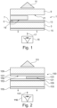
- Figure 1 shows a schematic cross-sectional view on a cover 1 according to the invention.
- Cover 1 comprises substrate 3, for example comprising molded clear polycarbonate.
- a first coating 7 in form of a reflective patterned metallic coating is provided on the side of a first surface 5 of the substrate 3.
- a second coating 9 preferably comprising a molded dark polycarbonate material is provided on the side of the first coating 7, being opposite to the substrate 3.
- an antenna in form of a radar unit 11 is covered.
- a third coating 13 in form of an insulating coating is provided in the first embodiment between the first coating 7 and the substrate 3.
- a fourth coating in form of a thermal hardcoat 15 is provided on the side of the substrate 3 being opposite to the first coating 7 and the third coating 13.
- Cover 1 may be produced by first providing the substrate 3, then depositing the third coating 13 onto the substrate 3 before depositing the first coating 7, for example by PVD magnetron sputtering.
- the first coating 7 includes a highly reflective metal material like chrome or aluminium.
- the first coating 7 is structured, for example by a CNC femtosecond laser. The laser allows to laser etch a pattern into the first coating 7 that provides a frequency selective surface band pass filter. The structure is described in more detail with the help of figures 3a to 3e later.
- the first coating 7 allows the first coating 7 to be transmissive for electromagnetic radiation in a first frequency band, especially that is emitted by the radar unit 11.
- the first coating 7 is highly reflective for electromagnetic radiation in a second frequency band, especially for visual electromagnetic radiation falling onto the first coating.
- the cover 1 does not negatively influence the functionality of the radar unit 11 but allows to provide an aesthetic visual outer appearance of cover 1.
- the second coating 9 is transmissive for the radiation of the first frequency band, so that radiation of the radar unit 11 can pass but is not transmissive for radiation of a third frequency band, that is preferably identical to the second frequency band, so that radiation in the visual wave lengths is blocked.
- a person 16 looking at the cover from a direction 17 sees an area 19 that is highly reflective and a more or less black area 21, screening the radar unit 11 from any visual light, so that a user 16 cannot see the radar unit 11 but only sees the structure or logo provided by the first coating 7.
- the area 21 appears to be black, whereas the area 19 has a lustrous appearance.
- FIG 2 a second embodiment of a claimed cover 100 is shown.
- the elements of cover 100 having the same functionalities as the respective elements in cover 1, have the same reference signs, however increased by 100.
- the first coating 107 is not restricted to a respective area but nearly covers the complete substrate 103.
- a masking layer 123 is used to generate the outer appearance of the wanted logo or emblem.
- a masking layer 123 is provided between the substrate 103 and the first coating 107.
- the masking layer 123 is, similar to the second coatings 9 or 109, non-transmissive for a radiation in a fifth frequency band, especially the second frequency band, but transmissive for radiation in the first frequency band.
- the masking layer 123 provides a black area for a user 16 looking at cover 101 from the direction 117.
- the area 119 provides a lustrous appearance whereas the area 121 provides an appearance as black for a user 116.
- the masking layer 123 is chosen such that it is transmissive for the electro-magnetic radiation provided by the radar unit 111, whereas it is non-transmissive for any electromagnetic radiation in the visual spectrum.
- second coatings 109 may be used.
- the second coating 109 might be completely omitted or might provide a protection for the coating 107 without the necessity of being non transmissive for radiation in the visual range as long as being transmissive for radiation in the first frequency band used by radar unit 11.
- the first coatings 7, 107 provide a frequency selective surface band pass filter.
- a frequency selective surface band pass filter is a thin, repetitive surface designed to reflect, transmit or absorb electromagnetic fields based on the different frequencies of the fields.
- the frequency selective surface is trimmed such that electromagnetic radiation of the first frequency band (used by unit 11, 111) is transmitted, whereas radiation in the second frequency band, especially visual light, is reflected.
- This aim is reached by providing a highly reflective coating being made of a highly reflective material like chrome or aluminium.
- a structure or pattern is formed, especially etched, to provide the transmissibility for the first frequency band.
- Such a pattern consists of elements having dimensions in the size smaller than 50 ⁇ m to not be seen too easily.
- elements having dimensions being greater than 50 ⁇ m and having distances of a few ⁇ m.
- the elements might have the form of crosses 201a, 201b, either completely filled like element 201b or having a center being left open like elements 201a.
- star form elements 203a, 203b or 203c might be used. Again these elements 203a, 203b, 203c, 203d might have left open centers like elements 203a, 203d or might be solid like elements 203b, 203c.
- Further examples of elements being formed iteratively in the pattern might comprise solid or left open circle form elements 205a, 205b, rectangular or quadratic form elements 207a, 207b and or hexagonally formed elements 209a, 209b as well as line elements 211.
- FIG 3a a schematic detail of a pattern 213 formed in coatings 7, 107 to provide a band pass filter, is shown.
- the pattern 213 comprises a repetitive structure in which the elements 215, here cross elements, are formed in a repetitive form.
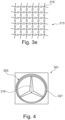
- FIG 4 a perspective view onto a cover 301 of the invention is shown.
- the area 321 appears to be black whereas areas 319 allow a view onto the first coating 307, providing a lustrous appearance.
- the visual appearance is increased as the star logo is provided and simultaneously the in Fig. 4 not shown radar unit is covered and not visible for the viewer.
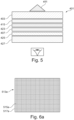
- FIG 5 a schematic cross-sectional view onto a third embodiment of an inventive cover 401 is shown.
- a substrate 403 in form of a moulded part made for example of a dark, i.e. for visual light opaque ABS, AES, PCABS, or polycarbonate is located on the side of the cover 401 facing the radar unit 411.
- the first coating 407 is located on the side of the substrate 403 being averted to the radar unit 411.
- an optional first fourth coating in form of a hardcoat 415 is located between the substrate 403 and the first coating 407.
- a stress controlling layer 423 may be also located between the substrate 403 and the first coating 407.
- the stress controlling layer 423 respective different mechanical characteristics of the substrate 403 and the first coating 407 and/or the hardcoat 415 are compensated.
- the substrate 403 and/or the hardcoat 415 might have different thermal expansions.
- these are compensated such that the forming of cracks or a separation of the first coating 407 from the substrate and/or the hardcoat 415 is avoided.
- the first coating 407 is covered by a covering layer 425 being transparent or semi-transparent for electromagnetic radiation in the visual range.
- the covering layer 427 might be covered by a second fourth coating in form of a hardcoat 427, optionally including light scattering particles. With the light scattering particles, the overall visual impression of the cover 401 is increased as the three-dimensional impression for a viewer is increased and the emblem formed by the pattern within the first coating 407 is visible over a broader angle of view.
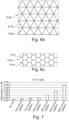
- FIG. 6a to 6c alternative patterns 513a, 513b, 513c, formed in the first coating 7, 107 or 407 as described above are shown.
- the pattern 513a shown in figure 6a is formed by a plurality of elements 515a, forming metallic "islands" that are separated from each other by openings or gaps 517a.
- the patterns 513a, 513b and 513c differ from each other that in figure 6a , the elements 515a have a square form whereas the elements 515b of the pattern 513b have the form of triangles whereas the elements 515c of pattern 513c have the form of pentagons.
- the openings 517b, 515c, that have been formed in the metallic coating by laser etching, have respective different forms compared to the openings 517a. It has been found by the inventors that the effectiveness of the frequency bandpass filter formed by the patterns 513a, 513b and 513c is increased, due to the separation of the metallic elements 515a, 515b and 515c, shown in white colours in figures 6a to 6c .
- the respective gaps separating the elements 515a, 515b and 515c from each other are shown in black colours in figures 6a to 6c .
- the inventors have compared the respective dimensions of the elements with respect to the attenuation for electromagnetic radiation in the frequency area of 76 to 77GHz. The result is shown in figure 7 .
- the size of the elements 515a, 515b and 515c should be ⁇ 400 ⁇ m, even better ⁇ 100 ⁇ m.
- the inventors assume that by these dimensions, the electrical disconnection of the metallic film elements is more efficient. In other words, the elements should have an area of less than 1600 ⁇ m 2 , even better less than 1000 ⁇ m 2 .
- the openings 517a, 517b and 517c should have dimensions, especially with less than 8 ⁇ m, even better less than 5 ⁇ m. In this way the openings 517a, 517b and 517c, preferably formed by ablation, cannot be easily seen by a user and thus the overall visual impression is not negatively influenced.
- the attenuation for the size of the elements of 500 ⁇ m, having an attenuation of about 3db, can be reduced to 0.3db when reducing the size of the elements to less than 100 ⁇ m.
- this attenuation comes close to this attenuation without a metal coating.
- the patterns 513a, 513b and 513c might be formed by applying an electrically conductive chrome coating, using PVD magnetron sputtering deposition to the hardcoated polycarbonate substrate.
- the respective openings 517a, 517b and 517c can be formed by placing the coated substrate on a CNC femtosecond laser system. By the laser system, the patterns are laser edged into the coating allowing it to act as a radome.
- Examples might be bidirectional lines forming 10 ⁇ m gaps with 500 ⁇ m metal squares in between, as shown in figures 6a .
- the gaps might have a width of 8 ⁇ m, preferably 6 ⁇ m, most preferably 3 ⁇ m, whereas the element 515a might have a side length of 200 ⁇ m, preferably 100 ⁇ m, most preferably less than 30 ⁇ m.
- the coated substrate is then placed in a moulding machine and a rear section of the badge is formed, encapsulating the first coating and completing the radome in form of the cover 401.
Landscapes
- Engineering & Computer Science (AREA)
- Remote Sensing (AREA)
- Computer Security & Cryptography (AREA)
- Radar, Positioning & Navigation (AREA)
- Aerials With Secondary Devices (AREA)
- Laminated Bodies (AREA)
- Details Of Aerials (AREA)
- Radar Systems Or Details Thereof (AREA)
Claims (16)
- Abdeckung (1, 101, 301, 401) für mindestens eine Antenne (11, 111, 411), die elektromagnetische Strahlung in mindestens einem ersten Frequenzbereich, der eine Radarfrequenz ist, aussendet und/oder erfasst, wobei die Abdeckung (1, 101, 301, 401) mindestens eine erste Oberfläche, die so ausgestaltet ist, dass sie der Antenne (11, 111, 411) zugewandt ist, und mindestens eine zweite Oberfläche, die so ausgestaltet ist, dass sie von der Antenne (11, 111, 411) abgewandt ist, umfasst, wobei die Abdeckung (1, 101, 301, 401) mindestens ein Substrat (3, 103, 403), das für elektromagnetische Strahlung des ersten Frequenzbereichs und eines zweiten Frequenzbereichs, der sichtbares Licht umfasst, durchlässig ist, und mindestens eine erste Beschichtung (7, 107, 407), die das Substrat (3, 103, 403) in mindestens einem ersten Bereich (19, 119) abdeckt, umfasst, wobei die erste Beschichtung (7, 107, 407) für elektromagnetische Strahlung mindestens des ersten Frequenzbereichs durchlässig ist und für elektromagnetische Strahlung, die auf die zweite Oberfläche auftrifft und eine Frequenz innerhalb des zweiten Frequenzbereichs aufweist, reflektierend ist, wobei die erste Beschichtung (7, 107, 407) dazu ausgestaltet ist, als Bandpassfilter mit frequenzselektiver Oberfläche zu fungieren, der so eingestellt ist, dass elektromagnetische Strahlung des ersten Frequenzbereichs durchgelassen wird, wohingegen Strahlung in dem zweiten Frequenzbereich reflektiert wird, wobei die Abdeckung ferner Folgendes umfasst:i) mindestens eine Abdeckungsschicht (425), die sich auf einer Seite der ersten Beschichtung (407), die von dem Substrat (403) abgewandt ist, befindet, wobei die Abdeckungsschicht für den zweiten Frequenzbereich transparent, zumindest semitransparent, ist, oderii) mindestens eine zweite Beschichtung (9, 109), die sich zumindest teilweise zwischen der ersten Beschichtung (7, 107) einerseits und der Antenne (11, 111) andererseits befindet, wobei die zweite Beschichtung (9, 109) in dem zweiten Frequenzbereich zumindest teilweise nicht durchlässig und/oder opak ist.
- Abdeckung nach Anspruch 1, dadurch gekennzeichnet, dass(i) die Antenne eine Radarantenne (11, 111, 411) ist und/oder der erste Frequenzbereich 10 GHz bis 130 GHz, vorzugsweise 20 GHz bis 100 GHz, noch bevorzugter 20 GHz bis 30 GHz, 70 GHz bis 80 GHz und/oder 90 GHz bis 100 GHz, am bevorzugtesten 24 GHz, 77 GHz oder 93 Ghz, ist,(ii) das Substrat (3, 103, 403) für elektromagnetische Strahlung in mindestens einem dritten Frequenzbereich durchlässig ist, wobei vorzugsweise der zweite Frequenzbereich zumindest teilweise mit dem dritten Frequenzbereich identisch ist, und/oder(iii) die erste Beschichtung (7, 107) sich zwischen dem Substrat (3, 103) und der Antenne (11, 111) befindet und/oder sich auf der Seite der ersten Oberfläche (5, 105) des Substrats (3, 103) befindet, die so ausgestaltet ist, dass sie der Antenne zugewandt ist.
- Abdeckung nach der/den Alternative(n) (i) und/oder (ii) von Anspruch 2, dadurch gekennzeichnet, dass die erste Beschichtung (407) sich auf der Seite der zweiten Oberfläche des Substrats (403) befindet, die so ausgestaltet ist, dass sie von der Antenne abgewandt ist, wobei vorzugsweise mindestens eine Beanspruchungssteuerungsschicht (423) sich zwischen dem Substrat (403) und der ersten Beschichtung (407) befindet.
- Abdeckung nach Anspruch 2, dadurch gekennzeichnet, dass(a) die zweite Beschichtung (9, 109) sich zumindest teilweise zwischen dem Substrat (3, 103) einerseits und der Antenne (11, 111) andererseits befindet und/oder die zweite Beschichtung (9, 109) in mindestens einem vierten Frequenzbereich, vorzugsweise dem dritten Frequenzbereich, zumindest teilweise nicht durchlässig und/oder opak und/oder in dem ersten Frequenzbereich durchlässig ist,(b) die Abdeckung durch mindestens eine Maskierungsschicht (23, 123), die zumindest teilweise die erste Beschichtung (7, 107) und/oder das Substrat (3, 103) abdeckt, gekennzeichnet ist, wobei die Maskierungsschicht (23, 123) in mindestens einem fünften Frequenzbereich, vorzugsweise dem zweiten Frequenzbereich, dem dritten Frequenzbereich und/oder dem vierten Frequenzbereich, zumindest teilweise nicht durchlässig und/oder opak und/oder in dem ersten Frequenzbereich durchlässig ist, und/oder(c) der zweite Frequenzbereich, der dritte Frequenzbereich und/oder der vierte Frequenzbereich 384 THz bis 789 THz und/oder sichtbares Licht umfasst, wobei vorzugsweise der zweite Frequenzbereich, der vierte Frequenzbereich und/oder der fünfte Frequenzbereich den Bereich von 384 THz bis 789 THz abdeckt/abdecken und/oder der dritte Frequenzbereich den Bereich von 384 THz bis 789 THz nur teilweise abdeckt.
- Abdeckung nach einem der vorangehenden Ansprüche, dadurch gekennzeichnet, dass(i) das Substrat (3, 103, 403) zumindest teilweise mindestens ein thermoplastisches Material, vorzugsweise Polycarbonat, Polymethylmethacrylat, Polyethylen, Polyester, Polyvinylchlorid, Polypropylen, Polystyrol, Acrylnitril-Butadien-Styrol, Acrylnitril-Ethylen-Styrol, Polyacrylat und/oder ein Gemisch davon, umfasst und/oder(ii) die erste Beschichtung (7, 107, 407) mindestens ein metallisches Material, vorzugsweise Chrom, Aluminium, Zink, Kupfer, Nickel, Vanadium, Titan, Zirkonium, Niob, Gold, Rhodium, Cobalt, Mangan, Molybdän, Tantal, Silber und/oder ein Gemisch davon, umfasst.
- Abdeckung nach Anspruch 4, dadurch gekennzeichnet, dass die Abdeckungsschicht (425) für den dritten, vierten und/oder fünften Frequenzbereich transparent, zumindest semitransparent, ist.
- Abdeckung nach einem der vorangehenden Ansprüche, dadurch gekennzeichnet, dass die erste Beschichtung (7, 107, 407) mindestens ein sich wiederholendes Muster (213, 513a, 513b, 513c) umfasst, wobei das Muster (213, 513a, 513b, 513c) vorzugsweise Folgendes umfasst: insbesondere eine Mehrzahl von Elementen (515a, 515b, 515c), die als Kreuze (201a, 201b, 201c, 201d), Kreise (205a, 205b), Quadrate (207a, 207b, 515a), Sterne (203a, 203b, 203c, 203d), Rechtecke (207a, 207b), Linien (211), Sechsecke (209a, 209b, 515c), Ellipsoide, Vielecke, Ring, Halbkreise, Kreissektoren, Triquetra, Lune, Arbelos, Spirale, Lemniskaten, Dreiecke (515b) und/oder ovale Formen ausgebildet sind, wobei gegebenenfalls die Elemente (201a, 201b, 201c, 201d, 203a, 203b, 203c, 203d, 205a, 205b, 207a, 207b, 209a, 209b) durch, insbesondere voneinander getrennte, Öffnungen und/oder Aussparungen innerhalb der ersten Beschichtung ausgebildet sind und/oder die Elemente (201a, 201b, 201c, 201d, 203a, 203b, 203c, 203d, 205a, 205b, 207a, 207b, 209a, 209b, 515a, 515b, 515c) durch, insbesondere voneinander getrennte und/oder nicht miteinander verbundene, Bereiche der ersten Beschichtung ausgebildet sind.
- Abdeckung nach einem der vorangehenden Ansprüche, dadurch gekennzeichnet, dass die zweite Beschichtung (9, 109) mindestens einen Thermoplasten, vorzugsweise Polycarbonat, Acrylnitril-Butadien-Styrol, Acrylnitril-Ethylen-Styrol und/oder Polycarbonat-Acrylnitril-Butadien-Styrol umfasst und/oder die erste Beschichtung (7, 107, 407), mit Blick auf die zweite Oberfläche der Abdeckung, mindestens ein Logo, ein Zeichen, eine Ziffer, eine Bildmarke, eine Marke, ein dekoratives Design und/oder ein dekoratives Muster aufweist.
- Abdeckung nach Anspruch 4, dadurch gekennzeichnet, dass die Maskierungsschicht (23, 123) mindestens einen Thermoplasten, vorzugsweise Polycarbonat, Acrylnitril-Butadien-Styrol, Acrylnitril-Ethylen-Styrol und/oder Polycarbonat-Acrylnitril-Butadien-Styrol, umfasst.
- Abdeckung nach Anspruch 4, dadurch gekennzeichnet, dass die Maskierungsschicht (123) die erste Beschichtung (107) derart abdeckt, dass, mit Blick auf die zweite Oberfläche, nur zumindest ein erster Bereich (119) der ersten Beschichtung (107) sichtbar ist, wobei der erste Bereich (119) die Form von mindestens einem Logo, einem Zeichen, einer Ziffer, einer Bildmarke, einer Marke, einem dekorativen Design und/oder einem dekorativen Muster aufweist, wobei der erste Bereich (119) zusammenhängend oder durch zumindest teilweise getrennte Unterbereiche ausgebildet ist.
- Abdeckung nach einem der vorangehenden Ansprüche, gekennzeichnet durch mindestens eine dritte Beschichtung (13, 113), die sich auf der ersten Oberfläche (5, 105) befindet, insbesondere zwischen dem Substrat (3, 103) und der ersten Beschichtung (7, 107), wobei die dritte Beschichtung (13, 113) insbesondere elektrisch isolierend ist, und/oder
gekennzeichnet durch mindestens eine vierte Beschichtung (15, 115, 415, 427), die sich vorzugsweise auf der zweiten Oberfläche und/oder der Seite der zweiten Oberfläche des Substrats (3, 103, 403), zwischen dem Substrat (403) und der ersten Beschichtung (407) und/oder der Abdeckungsschicht, befindet und/oder sich auf der Seite der ersten Beschichtung und/oder der Abdeckungsschicht, die von dem Substrat abgewandt ist, befindet, wobei die vierte Beschichtung (15, 115, 415, 427) insbesondere eine thermische Hartschicht (15, 115, 415, 427) ausbildet, die gegebenenfalls lichtstreuende Teilchen umfasst. - Abdeckung nach einem der vorangehenden Ansprüche, dadurch gekennzeichnet, dass die erste Beschichtung (7, 107, 407) mehr als 50 %, vorzugsweise mehr als 75 %, besonders bevorzugt mehr als 85 %, noch mehr bevorzugt mehr als 90 %, am bevorzugtesten mehr als 95 %, reflektiert und/oder die erste Beschichtung (7, 107, 407) mindestens einen Rand aufweist, der zumindest teilweise gekrümmt ist, und/oder die erste Beschichtung (7, 107, 407), insbesondere im Bereich des Randes, mindestens eine ohmsche Belastung umfasst.
- Verfahren zum Herstellen einer Abdeckung (1, 101, 401) für mindestens eine Antenne (11, 111, 411), die elektromagnetische Strahlung in mindestens einem ersten Frequenzbereich, der eine Radarfrequenz ist, aussendet und/oder erfasst, insbesondere einer Abdeckung (1, 101, 401) nach einem der vorangehenden Ansprüche, wobei das Verfahren folgende Schritte umfasst:Bereitstellen und/oder Herstellen mindestens eines Substrats (3, 103, 403), das für elektromagnetische Strahlung des ersten Frequenzbereichs und eines zweiten Frequenzbereichs, der sichtbares Licht umfasst, durchlässig ist,Abdecken des Substrats (3, 103, 403) mit mindestens einer ersten Beschichtung (7, 107, 407), wobei die erste Beschichtung (7, 107, 407) einen Bandpassfilter mit frequenzselektiver Oberfläche bereitstellt, der für Strahlung, die eine Frequenz in dem ersten Frequenzbereich aufweist, durchlässig ist, wobei als erste Beschichtung (7, 107, 407) ein Material, das für Frequenzen in dem zweiten Frequenzbereich hoch reflektierend ist, verwendet wird, wobei das Verfahren ferner Folgendes umfasst:i) Anordnen mindestens einer Abdeckungsschicht (425) auf einer Seite der ersten Beschichtung (407), die von dem Substrat (403) abgewandt ist, wobei die Abdeckungsschicht für den zweiten Frequenzbereich transparent, zumindest semitransparent, ist, oderii) zumindest teilweises Anordnen einer zweiten Beschichtung (9, 109) zwischen der ersten Beschichtung (7, 107) einerseits und der Antenne (11, 111) andererseits, wobei die zweite Beschichtung (9, 109) in dem zweiten Frequenzbereich zumindest teilweise nicht durchlässig und/oder opak ist.
- Verfahren nach Anspruch 13, gekennzeichnet durch Abdecken des Substrats (3, 103) mit mindestens einer Maskierungsschicht (23, 123), die für elektromagnetische Strahlung in dem zweiten Frequenzbereich nicht durchlässig ist, wobei vorzugsweise das Substrat (3, 103) mit der Maskierungsschicht (23, 123) abgedeckt wird, bevor das Substrat (3, 103) mit der ersten Beschichtung (7, 107) abgedeckt wird, wobei insbesondere die erste Beschichtung (7, 107) sich zumindest teilweise auf der Maskierungsschicht (23, 123) befindet, und/oder dadurch gekennzeichnet, dass der Bandpassfilter mit frequenzselektiver Oberfläche durch Strukturieren der ersten Beschichtung (7, 107, 407) nach ihrer Abscheidung auf das Substrat (3, 103, 403) hergestellt wird, vorzugsweise durch Laserätzen, wobei vorzugsweise das Strukturieren das Ausbilden einer Mehrzahl von Elementen (201a, 201b, 201c, 201d, 203a, 203b, 203c, 203d, 205a, 205b, 207a, 207b, 209a, 209b, 515a, 515b, 515c), die ein Muster (213, 513a, 513b, 513c) ausbilden, umfasst, wobei die Elemente (201a, 201b, 201c, 201d, 203a, 203b, 203c, 203d, 205a, 205b, 207a, 207b, 209a, 209b, 515a, 515b, 515c) insbesondere, vorzugsweise voneinander getrennte, Öffnungen und/oder Aussparungen innerhalb der ersten Beschichtung umfasst und/oder, vorzugsweise voneinander getrennte, insbesondere durch die Aussparungen und/oder Öffnungen (517a, 517b, 517c) getrennte, Bereiche der ersten Beschichtung (407) umfasst.
- Verfahren nach Anspruch 13 oder 14, dadurch gekennzeichnet, dass die erste Beschichtung (7, 107, 407) durch Sputtern, insbesondere PVD-Magnetron-Sputter-Deposition, hergestellt wird.
- Verfahren nach einem der Ansprüche 13 bis 15, dadurch gekennzeichnet, dass das Verfahren ferner das Bereitstellen von Folgendem umfasst:(a) mindestens eine erste vierte, vorzugsweise mindestens eine Hartschicht (415) ausbildende, Beschichtung und/oder mindestens eine Beanspruchungssteuerungsschicht (423), die sich zumindest teilweise zwischen dem Substrat (403) und der ersten Beschichtung (407) befindet, und/oder(b) mindestens eine zweite vierte, mindestens eine Hartschicht (427) ausbildende, Beschichtung, die sich zumindest teilweise auf der Seite der ersten Beschichtung, die von dem Substrat abgewandt ist, befindet, und/oder mindestens eine Abdeckungsschicht, die insbesondere für sichtbares Licht und/oder elektromagnetische Strahlung in einem Frequenzbereich, der zumindest teilweise 384 THz bis 789 THz umfasst, transparent, zumindest semitransparent, ist.
Applications Claiming Priority (3)
| Application Number | Priority Date | Filing Date | Title |
|---|---|---|---|
| DE102019100669.4A DE102019100669A1 (de) | 2019-01-11 | 2019-01-11 | Elektromagnetischer Störschutz für Radome |
| PCT/EP2019/077800 WO2020078916A2 (en) | 2018-10-15 | 2019-10-14 | Decorative radome and method of producing the same |
| PCT/EP2020/050580 WO2020144351A1 (en) | 2019-01-11 | 2020-01-10 | Electromagnetic interference protection for radomes |
Publications (2)
| Publication Number | Publication Date |
|---|---|
| EP3909096A1 EP3909096A1 (de) | 2021-11-17 |
| EP3909096B1 true EP3909096B1 (de) | 2024-01-03 |
Family
ID=71132108
Family Applications (1)
| Application Number | Title | Priority Date | Filing Date |
|---|---|---|---|
| EP20700681.8A Active EP3909096B1 (de) | 2019-01-11 | 2020-01-10 | Schutz vor elektromagnetischer störung für radome |
Country Status (5)
| Country | Link |
|---|---|
| US (2) | US11764467B2 (de) |
| EP (1) | EP3909096B1 (de) |
| JP (1) | JP7610512B2 (de) |
| DE (1) | DE102019100669A1 (de) |
| WO (1) | WO2020144351A1 (de) |
Families Citing this family (8)
| Publication number | Priority date | Publication date | Assignee | Title |
|---|---|---|---|---|
| EP4142048B1 (de) * | 2021-08-30 | 2026-05-06 | Motherson Innovations Company Limited | Dekorative pvd-beschichtete gegenstände und radome und verfahren zu deren herstellung |
| DE102021128982A1 (de) * | 2021-11-08 | 2023-05-11 | Marelli Automotive Lighting Reutlingen (Germany) GmbH | Sensorvorrichtung |
| CN114114155A (zh) * | 2021-11-16 | 2022-03-01 | 英博超算(南京)科技有限公司 | 一种雷达覆盖件 |
| TR2022004865A1 (tr) * | 2022-03-29 | 2023-10-23 | İstanbul Tekni̇k Üni̇versi̇tesi̇ | Atrp yöntemi̇ i̇le sentezlenerek hi̇drofi̇li̇k özelli̇kleri̇ modi̇fi̇ye edi̇lmi̇ş pmma/ boraks kompozi̇ti̇n geni̇ş bant (500 mhz ? 50 ghz) di̇elekti̇ri̇k katsayisinin geli̇şti̇ri̇lmesi̇ tekni̇ği̇ ve potansi̇yel uygulama alanlari |
| JP7811510B2 (ja) * | 2022-04-20 | 2026-02-05 | 横浜ゴム株式会社 | マントルクローク組み込みレドーム |
| JP2024074129A (ja) * | 2022-11-18 | 2024-05-30 | 豊田合成株式会社 | 電磁波透過カバー及びセンサモジュール |
| WO2025115090A1 (ja) * | 2023-11-28 | 2025-06-05 | 日産自動車株式会社 | 積層構造体 |
| KR102841144B1 (ko) * | 2024-06-25 | 2025-07-31 | 주식회사 케이앤에스아이앤씨 | 고내수압을 갖는 잠수함용 위성안테나 레이돔 |
Family Cites Families (17)
| Publication number | Priority date | Publication date | Assignee | Title |
|---|---|---|---|---|
| US5468409A (en) | 1993-11-03 | 1995-11-21 | The Boeing Company | Copper etchant useful for making fine-line copper elements |
| DE19819709C2 (de) * | 1998-05-02 | 2000-05-25 | Daimler Chrysler Ag | Verfahren zur Herstellung eines Radoms für ein Abstandswarnradar und Radom für ein Abstandswarnradar |
| DE10028801A1 (de) * | 2000-06-15 | 2001-12-20 | Volkswagen Ag | Radom für einen Radarsensor |
| FR2827080A1 (fr) * | 2001-07-06 | 2003-01-10 | Thales Sa | Dispositif pour cacher un radar representant un motif en volume, equipant notamment un vehicule et systeme de detection comportant un tel dispositif |
| US6730389B2 (en) * | 2001-10-25 | 2004-05-04 | Ppg Industries Ohio, Inc. | Coated substrate having a frequency selective surface |
| JP4224794B2 (ja) * | 2002-12-26 | 2009-02-18 | 豊田合成株式会社 | 電波透過カバーの製造方法 |
| US8185166B2 (en) * | 2008-10-24 | 2012-05-22 | Apple Inc. | Thermal spray coating for seamless and radio-transparent electronic device housing |
| JP5560555B2 (ja) * | 2008-11-06 | 2014-07-30 | トヨタ自動車株式会社 | 車両用電波透過カバーの製造方法 |
| JP5275856B2 (ja) * | 2009-03-16 | 2013-08-28 | 株式会社東海理化電機製作所 | 装飾部材、レーダユニット、装飾部材製造方法 |
| JP5841063B2 (ja) * | 2009-12-24 | 2016-01-06 | エスエムアール・パテンツ・ソシエテ・ア・レスポンサビリテ・リミテ | プラスチック製自動車用ミラー |
| US9114760B2 (en) * | 2010-11-15 | 2015-08-25 | Zanini Auto Grup, Sa | Decorative radome for automotive vehicular applications |
| JP6511474B2 (ja) * | 2014-03-07 | 2019-05-15 | ユニヴァーシティ・オブ・サウス・オーストラリア | プラスチック基板のための装飾コーティング |
| KR20160006545A (ko) | 2014-07-09 | 2016-01-19 | (주)휴맥스 | 입력 장치와의 매핑을 통해 분할된 스크린을 개별 제어하기 위한 시스템 및 방법 |
| JP2016080479A (ja) * | 2014-10-15 | 2016-05-16 | 豊田合成株式会社 | 電波透過性カバー |
| JP6440123B2 (ja) * | 2015-05-19 | 2018-12-19 | パナソニックIpマネジメント株式会社 | アンテナ装置、無線通信装置、及びレーダ装置 |
| DE102015217744A1 (de) * | 2015-09-16 | 2017-03-16 | Nanogate PD Systems GmbH | Radom |
| US20180159207A1 (en) * | 2016-12-02 | 2018-06-07 | Srg Global Inc. | Multi-piece vehicle radome having non-uniform back piece |
-
2019
- 2019-01-11 DE DE102019100669.4A patent/DE102019100669A1/de not_active Ceased
-
2020
- 2020-01-10 WO PCT/EP2020/050580 patent/WO2020144351A1/en not_active Ceased
- 2020-01-10 JP JP2021538981A patent/JP7610512B2/ja active Active
- 2020-01-10 EP EP20700681.8A patent/EP3909096B1/de active Active
-
2021
- 2021-07-07 US US17/369,364 patent/US11764467B2/en active Active
-
2023
- 2023-08-11 US US18/448,209 patent/US12525709B2/en active Active
Also Published As
| Publication number | Publication date |
|---|---|
| JP7610512B2 (ja) | 2025-01-08 |
| US20210344110A1 (en) | 2021-11-04 |
| US12525709B2 (en) | 2026-01-13 |
| US20230387582A1 (en) | 2023-11-30 |
| EP3909096A1 (de) | 2021-11-17 |
| JP2022516921A (ja) | 2022-03-03 |
| DE102019100669A1 (de) | 2020-07-16 |
| WO2020144351A1 (en) | 2020-07-16 |
| US11764467B2 (en) | 2023-09-19 |
Similar Documents
| Publication | Publication Date | Title |
|---|---|---|
| US12525709B2 (en) | Electromagnetic interference protection for radomes | |
| EP2640609B1 (de) | Dekoratives radom für automobilanwendungen | |
| EP3563449B1 (de) | Radom für fahrzeuge | |
| EP3482453B1 (de) | Radom für fahrzeuge | |
| EP3549197B1 (de) | Mehrteiliges radom mit uneinheitlichem rückseitigem teil für ein kraftfahrzeug | |
| US6184842B1 (en) | Process for manufacturing a radome for a range warning radar | |
| US11827158B2 (en) | Radome for vehicles | |
| US20030052810A1 (en) | Device to conceal a radar representing a pattern in relief, equipping especially a vehicle, and detection system comprising such a device | |
| JP2006264593A (ja) | レーダ装置ビーム経路内用光輝装飾成形品 | |
| JP2006267019A (ja) | レーダ装置ビーム経路内用光輝装飾成形品 | |
| JP2007013722A (ja) | 電波レーダ装置のビーム経路に配置される樹脂成形品とその製造方法 | |
| US6750819B2 (en) | Sensor cover and method of construction thereof | |
| US20020171579A1 (en) | Vehicle radar concealment device bearing a pattern, and method for making such a device | |
| EP3739685B1 (de) | Radom für fahrzeuge | |
| US6246381B1 (en) | Insert mold process for forming polarizing grid element |
Legal Events
| Date | Code | Title | Description |
|---|---|---|---|
| STAA | Information on the status of an ep patent application or granted ep patent |
Free format text: STATUS: UNKNOWN |
|
| STAA | Information on the status of an ep patent application or granted ep patent |
Free format text: STATUS: THE INTERNATIONAL PUBLICATION HAS BEEN MADE |
|
| PUAI | Public reference made under article 153(3) epc to a published international application that has entered the european phase |
Free format text: ORIGINAL CODE: 0009012 |
|
| STAA | Information on the status of an ep patent application or granted ep patent |
Free format text: STATUS: REQUEST FOR EXAMINATION WAS MADE |
|
| 17P | Request for examination filed |
Effective date: 20210809 |
|
| AK | Designated contracting states |
Kind code of ref document: A1 Designated state(s): AL AT BE BG CH CY CZ DE DK EE ES FI FR GB GR HR HU IE IS IT LI LT LU LV MC MK MT NL NO PL PT RO RS SE SI SK SM TR |
|
| RAP3 | Party data changed (applicant data changed or rights of an application transferred) |
Owner name: MOTHERSON INNOVATIONS COMPANY LIMITED |
|
| DAV | Request for validation of the european patent (deleted) | ||
| DAX | Request for extension of the european patent (deleted) | ||
| RAP3 | Party data changed (applicant data changed or rights of an application transferred) |
Owner name: MOTHERSON INNOVATIONS COMPANY LIMITED |
|
| STAA | Information on the status of an ep patent application or granted ep patent |
Free format text: STATUS: EXAMINATION IS IN PROGRESS |
|
| 17Q | First examination report despatched |
Effective date: 20230425 |
|
| GRAP | Despatch of communication of intention to grant a patent |
Free format text: ORIGINAL CODE: EPIDOSNIGR1 |
|
| STAA | Information on the status of an ep patent application or granted ep patent |
Free format text: STATUS: GRANT OF PATENT IS INTENDED |
|
| INTG | Intention to grant announced |
Effective date: 20230616 |
|
| P01 | Opt-out of the competence of the unified patent court (upc) registered |
Effective date: 20230616 |
|
| GRAS | Grant fee paid |
Free format text: ORIGINAL CODE: EPIDOSNIGR3 |
|
| GRAJ | Information related to disapproval of communication of intention to grant by the applicant or resumption of examination proceedings by the epo deleted |
Free format text: ORIGINAL CODE: EPIDOSDIGR1 |
|
| GRAL | Information related to payment of fee for publishing/printing deleted |
Free format text: ORIGINAL CODE: EPIDOSDIGR3 |
|
| STAA | Information on the status of an ep patent application or granted ep patent |
Free format text: STATUS: EXAMINATION IS IN PROGRESS |
|
| GRAP | Despatch of communication of intention to grant a patent |
Free format text: ORIGINAL CODE: EPIDOSNIGR1 |
|
| STAA | Information on the status of an ep patent application or granted ep patent |
Free format text: STATUS: GRANT OF PATENT IS INTENDED |
|
| INTC | Intention to grant announced (deleted) | ||
| GRAA | (expected) grant |
Free format text: ORIGINAL CODE: 0009210 |
|
| STAA | Information on the status of an ep patent application or granted ep patent |
Free format text: STATUS: THE PATENT HAS BEEN GRANTED |
|
| INTG | Intention to grant announced |
Effective date: 20231114 |
|
| AK | Designated contracting states |
Kind code of ref document: B1 Designated state(s): AL AT BE BG CH CY CZ DE DK EE ES FI FR GB GR HR HU IE IS IT LI LT LU LV MC MK MT NL NO PL PT RO RS SE SI SK SM TR |
|
| REG | Reference to a national code |
Ref country code: GB Ref legal event code: FG4D |
|
| REG | Reference to a national code |
Ref country code: CH Ref legal event code: EP |
|
| REG | Reference to a national code |
Ref country code: DE Ref legal event code: R096 Ref document number: 602020023788 Country of ref document: DE |
|
| REG | Reference to a national code |
Ref country code: IE Ref legal event code: FG4D |
|
| REG | Reference to a national code |
Ref country code: DE Ref legal event code: R084 Ref document number: 602020023788 Country of ref document: DE |
|
| REG | Reference to a national code |
Ref country code: LT Ref legal event code: MG9D |
|
| PG25 | Lapsed in a contracting state [announced via postgrant information from national office to epo] |
Ref country code: ES Free format text: LAPSE BECAUSE OF FAILURE TO SUBMIT A TRANSLATION OF THE DESCRIPTION OR TO PAY THE FEE WITHIN THE PRESCRIBED TIME-LIMIT Effective date: 20240103 |
|
| PG25 | Lapsed in a contracting state [announced via postgrant information from national office to epo] |
Ref country code: ES Free format text: LAPSE BECAUSE OF FAILURE TO SUBMIT A TRANSLATION OF THE DESCRIPTION OR TO PAY THE FEE WITHIN THE PRESCRIBED TIME-LIMIT Effective date: 20240103 |
|
| REG | Reference to a national code |
Ref country code: NL Ref legal event code: MP Effective date: 20240103 |
|
| REG | Reference to a national code |
Ref country code: AT Ref legal event code: MK05 Ref document number: 1647749 Country of ref document: AT Kind code of ref document: T Effective date: 20240103 |
|
| PG25 | Lapsed in a contracting state [announced via postgrant information from national office to epo] |
Ref country code: NL Free format text: LAPSE BECAUSE OF FAILURE TO SUBMIT A TRANSLATION OF THE DESCRIPTION OR TO PAY THE FEE WITHIN THE PRESCRIBED TIME-LIMIT Effective date: 20240103 |
|
| PG25 | Lapsed in a contracting state [announced via postgrant information from national office to epo] |
Ref country code: NL Free format text: LAPSE BECAUSE OF FAILURE TO SUBMIT A TRANSLATION OF THE DESCRIPTION OR TO PAY THE FEE WITHIN THE PRESCRIBED TIME-LIMIT Effective date: 20240103 |
|
| PG25 | Lapsed in a contracting state [announced via postgrant information from national office to epo] |
Ref country code: IS Free format text: LAPSE BECAUSE OF FAILURE TO SUBMIT A TRANSLATION OF THE DESCRIPTION OR TO PAY THE FEE WITHIN THE PRESCRIBED TIME-LIMIT Effective date: 20240503 |
|
| PG25 | Lapsed in a contracting state [announced via postgrant information from national office to epo] |
Ref country code: LT Free format text: LAPSE BECAUSE OF FAILURE TO SUBMIT A TRANSLATION OF THE DESCRIPTION OR TO PAY THE FEE WITHIN THE PRESCRIBED TIME-LIMIT Effective date: 20240103 |
|
| PG25 | Lapsed in a contracting state [announced via postgrant information from national office to epo] |
Ref country code: GR Free format text: LAPSE BECAUSE OF FAILURE TO SUBMIT A TRANSLATION OF THE DESCRIPTION OR TO PAY THE FEE WITHIN THE PRESCRIBED TIME-LIMIT Effective date: 20240404 |
|
| PG25 | Lapsed in a contracting state [announced via postgrant information from national office to epo] |
Ref country code: HR Free format text: LAPSE BECAUSE OF FAILURE TO SUBMIT A TRANSLATION OF THE DESCRIPTION OR TO PAY THE FEE WITHIN THE PRESCRIBED TIME-LIMIT Effective date: 20240103 Ref country code: RS Free format text: LAPSE BECAUSE OF FAILURE TO SUBMIT A TRANSLATION OF THE DESCRIPTION OR TO PAY THE FEE WITHIN THE PRESCRIBED TIME-LIMIT Effective date: 20240403 |
|
| PG25 | Lapsed in a contracting state [announced via postgrant information from national office to epo] |
Ref country code: AT Free format text: LAPSE BECAUSE OF FAILURE TO SUBMIT A TRANSLATION OF THE DESCRIPTION OR TO PAY THE FEE WITHIN THE PRESCRIBED TIME-LIMIT Effective date: 20240103 Ref country code: CZ Free format text: LAPSE BECAUSE OF FAILURE TO SUBMIT A TRANSLATION OF THE DESCRIPTION OR TO PAY THE FEE WITHIN THE PRESCRIBED TIME-LIMIT Effective date: 20240103 |
|
| PG25 | Lapsed in a contracting state [announced via postgrant information from national office to epo] |
Ref country code: RS Free format text: LAPSE BECAUSE OF FAILURE TO SUBMIT A TRANSLATION OF THE DESCRIPTION OR TO PAY THE FEE WITHIN THE PRESCRIBED TIME-LIMIT Effective date: 20240403 Ref country code: NO Free format text: LAPSE BECAUSE OF FAILURE TO SUBMIT A TRANSLATION OF THE DESCRIPTION OR TO PAY THE FEE WITHIN THE PRESCRIBED TIME-LIMIT Effective date: 20240403 Ref country code: LT Free format text: LAPSE BECAUSE OF FAILURE TO SUBMIT A TRANSLATION OF THE DESCRIPTION OR TO PAY THE FEE WITHIN THE PRESCRIBED TIME-LIMIT Effective date: 20240103 Ref country code: IS Free format text: LAPSE BECAUSE OF FAILURE TO SUBMIT A TRANSLATION OF THE DESCRIPTION OR TO PAY THE FEE WITHIN THE PRESCRIBED TIME-LIMIT Effective date: 20240503 Ref country code: HR Free format text: LAPSE BECAUSE OF FAILURE TO SUBMIT A TRANSLATION OF THE DESCRIPTION OR TO PAY THE FEE WITHIN THE PRESCRIBED TIME-LIMIT Effective date: 20240103 Ref country code: GR Free format text: LAPSE BECAUSE OF FAILURE TO SUBMIT A TRANSLATION OF THE DESCRIPTION OR TO PAY THE FEE WITHIN THE PRESCRIBED TIME-LIMIT Effective date: 20240404 Ref country code: CZ Free format text: LAPSE BECAUSE OF FAILURE TO SUBMIT A TRANSLATION OF THE DESCRIPTION OR TO PAY THE FEE WITHIN THE PRESCRIBED TIME-LIMIT Effective date: 20240103 Ref country code: BG Free format text: LAPSE BECAUSE OF FAILURE TO SUBMIT A TRANSLATION OF THE DESCRIPTION OR TO PAY THE FEE WITHIN THE PRESCRIBED TIME-LIMIT Effective date: 20240103 Ref country code: AT Free format text: LAPSE BECAUSE OF FAILURE TO SUBMIT A TRANSLATION OF THE DESCRIPTION OR TO PAY THE FEE WITHIN THE PRESCRIBED TIME-LIMIT Effective date: 20240103 |
|
| PG25 | Lapsed in a contracting state [announced via postgrant information from national office to epo] |
Ref country code: PL Free format text: LAPSE BECAUSE OF FAILURE TO SUBMIT A TRANSLATION OF THE DESCRIPTION OR TO PAY THE FEE WITHIN THE PRESCRIBED TIME-LIMIT Effective date: 20240103 Ref country code: PT Free format text: LAPSE BECAUSE OF FAILURE TO SUBMIT A TRANSLATION OF THE DESCRIPTION OR TO PAY THE FEE WITHIN THE PRESCRIBED TIME-LIMIT Effective date: 20240503 |
|
| PG25 | Lapsed in a contracting state [announced via postgrant information from national office to epo] |
Ref country code: SE Free format text: LAPSE BECAUSE OF FAILURE TO SUBMIT A TRANSLATION OF THE DESCRIPTION OR TO PAY THE FEE WITHIN THE PRESCRIBED TIME-LIMIT Effective date: 20240103 Ref country code: PT Free format text: LAPSE BECAUSE OF FAILURE TO SUBMIT A TRANSLATION OF THE DESCRIPTION OR TO PAY THE FEE WITHIN THE PRESCRIBED TIME-LIMIT Effective date: 20240503 Ref country code: PL Free format text: LAPSE BECAUSE OF FAILURE TO SUBMIT A TRANSLATION OF THE DESCRIPTION OR TO PAY THE FEE WITHIN THE PRESCRIBED TIME-LIMIT Effective date: 20240103 Ref country code: LV Free format text: LAPSE BECAUSE OF FAILURE TO SUBMIT A TRANSLATION OF THE DESCRIPTION OR TO PAY THE FEE WITHIN THE PRESCRIBED TIME-LIMIT Effective date: 20240103 |
|
| REG | Reference to a national code |
Ref country code: CH Ref legal event code: PL |
|
| PG25 | Lapsed in a contracting state [announced via postgrant information from national office to epo] |
Ref country code: LU Free format text: LAPSE BECAUSE OF NON-PAYMENT OF DUE FEES Effective date: 20240110 |
|
| PG25 | Lapsed in a contracting state [announced via postgrant information from national office to epo] |
Ref country code: LU Free format text: LAPSE BECAUSE OF NON-PAYMENT OF DUE FEES Effective date: 20240110 |
|
| REG | Reference to a national code |
Ref country code: DE Ref legal event code: R097 Ref document number: 602020023788 Country of ref document: DE |
|
| PG25 | Lapsed in a contracting state [announced via postgrant information from national office to epo] |
Ref country code: DK Free format text: LAPSE BECAUSE OF FAILURE TO SUBMIT A TRANSLATION OF THE DESCRIPTION OR TO PAY THE FEE WITHIN THE PRESCRIBED TIME-LIMIT Effective date: 20240103 |
|
| PG25 | Lapsed in a contracting state [announced via postgrant information from national office to epo] |
Ref country code: SM Free format text: LAPSE BECAUSE OF FAILURE TO SUBMIT A TRANSLATION OF THE DESCRIPTION OR TO PAY THE FEE WITHIN THE PRESCRIBED TIME-LIMIT Effective date: 20240103 |
|
| PG25 | Lapsed in a contracting state [announced via postgrant information from national office to epo] |
Ref country code: BE Free format text: LAPSE BECAUSE OF NON-PAYMENT OF DUE FEES Effective date: 20240131 |
|
| PG25 | Lapsed in a contracting state [announced via postgrant information from national office to epo] |
Ref country code: CH Free format text: LAPSE BECAUSE OF NON-PAYMENT OF DUE FEES Effective date: 20240131 |
|
| PG25 | Lapsed in a contracting state [announced via postgrant information from national office to epo] |
Ref country code: EE Free format text: LAPSE BECAUSE OF FAILURE TO SUBMIT A TRANSLATION OF THE DESCRIPTION OR TO PAY THE FEE WITHIN THE PRESCRIBED TIME-LIMIT Effective date: 20240103 |
|
| PG25 | Lapsed in a contracting state [announced via postgrant information from national office to epo] |
Ref country code: SK Free format text: LAPSE BECAUSE OF FAILURE TO SUBMIT A TRANSLATION OF THE DESCRIPTION OR TO PAY THE FEE WITHIN THE PRESCRIBED TIME-LIMIT Effective date: 20240103 |
|
| PG25 | Lapsed in a contracting state [announced via postgrant information from national office to epo] |
Ref country code: SM Free format text: LAPSE BECAUSE OF FAILURE TO SUBMIT A TRANSLATION OF THE DESCRIPTION OR TO PAY THE FEE WITHIN THE PRESCRIBED TIME-LIMIT Effective date: 20240103 Ref country code: SK Free format text: LAPSE BECAUSE OF FAILURE TO SUBMIT A TRANSLATION OF THE DESCRIPTION OR TO PAY THE FEE WITHIN THE PRESCRIBED TIME-LIMIT Effective date: 20240103 Ref country code: RO Free format text: LAPSE BECAUSE OF FAILURE TO SUBMIT A TRANSLATION OF THE DESCRIPTION OR TO PAY THE FEE WITHIN THE PRESCRIBED TIME-LIMIT Effective date: 20240103 Ref country code: EE Free format text: LAPSE BECAUSE OF FAILURE TO SUBMIT A TRANSLATION OF THE DESCRIPTION OR TO PAY THE FEE WITHIN THE PRESCRIBED TIME-LIMIT Effective date: 20240103 Ref country code: DK Free format text: LAPSE BECAUSE OF FAILURE TO SUBMIT A TRANSLATION OF THE DESCRIPTION OR TO PAY THE FEE WITHIN THE PRESCRIBED TIME-LIMIT Effective date: 20240103 Ref country code: CH Free format text: LAPSE BECAUSE OF NON-PAYMENT OF DUE FEES Effective date: 20240131 Ref country code: BE Free format text: LAPSE BECAUSE OF NON-PAYMENT OF DUE FEES Effective date: 20240131 |
|
| REG | Reference to a national code |
Ref country code: BE Ref legal event code: MM Effective date: 20240131 |
|
| PLBE | No opposition filed within time limit |
Free format text: ORIGINAL CODE: 0009261 |
|
| STAA | Information on the status of an ep patent application or granted ep patent |
Free format text: STATUS: NO OPPOSITION FILED WITHIN TIME LIMIT |
|
| PG25 | Lapsed in a contracting state [announced via postgrant information from national office to epo] |
Ref country code: MC Free format text: LAPSE BECAUSE OF FAILURE TO SUBMIT A TRANSLATION OF THE DESCRIPTION OR TO PAY THE FEE WITHIN THE PRESCRIBED TIME-LIMIT Effective date: 20240103 |
|
| PG25 | Lapsed in a contracting state [announced via postgrant information from national office to epo] |
Ref country code: MC Free format text: LAPSE BECAUSE OF FAILURE TO SUBMIT A TRANSLATION OF THE DESCRIPTION OR TO PAY THE FEE WITHIN THE PRESCRIBED TIME-LIMIT Effective date: 20240103 |
|
| PG25 | Lapsed in a contracting state [announced via postgrant information from national office to epo] |
Ref country code: IT Free format text: LAPSE BECAUSE OF FAILURE TO SUBMIT A TRANSLATION OF THE DESCRIPTION OR TO PAY THE FEE WITHIN THE PRESCRIBED TIME-LIMIT Effective date: 20240103 |
|
| 26N | No opposition filed |
Effective date: 20241007 |
|
| PG25 | Lapsed in a contracting state [announced via postgrant information from national office to epo] |
Ref country code: IT Free format text: LAPSE BECAUSE OF FAILURE TO SUBMIT A TRANSLATION OF THE DESCRIPTION OR TO PAY THE FEE WITHIN THE PRESCRIBED TIME-LIMIT Effective date: 20240103 |
|
| PG25 | Lapsed in a contracting state [announced via postgrant information from national office to epo] |
Ref country code: IE Free format text: LAPSE BECAUSE OF NON-PAYMENT OF DUE FEES Effective date: 20240110 |
|
| PG25 | Lapsed in a contracting state [announced via postgrant information from national office to epo] |
Ref country code: IE Free format text: LAPSE BECAUSE OF NON-PAYMENT OF DUE FEES Effective date: 20240110 |
|
| PG25 | Lapsed in a contracting state [announced via postgrant information from national office to epo] |
Ref country code: SI Free format text: LAPSE BECAUSE OF FAILURE TO SUBMIT A TRANSLATION OF THE DESCRIPTION OR TO PAY THE FEE WITHIN THE PRESCRIBED TIME-LIMIT Effective date: 20240103 |
|
| PG25 | Lapsed in a contracting state [announced via postgrant information from national office to epo] |
Ref country code: CY Free format text: LAPSE BECAUSE OF FAILURE TO SUBMIT A TRANSLATION OF THE DESCRIPTION OR TO PAY THE FEE WITHIN THE PRESCRIBED TIME-LIMIT; INVALID AB INITIO Effective date: 20200110 |
|
| PG25 | Lapsed in a contracting state [announced via postgrant information from national office to epo] |
Ref country code: HU Free format text: LAPSE BECAUSE OF FAILURE TO SUBMIT A TRANSLATION OF THE DESCRIPTION OR TO PAY THE FEE WITHIN THE PRESCRIBED TIME-LIMIT; INVALID AB INITIO Effective date: 20200110 |
|
| PG25 | Lapsed in a contracting state [announced via postgrant information from national office to epo] |
Ref country code: FI Free format text: LAPSE BECAUSE OF FAILURE TO SUBMIT A TRANSLATION OF THE DESCRIPTION OR TO PAY THE FEE WITHIN THE PRESCRIBED TIME-LIMIT Effective date: 20240103 |
|
| PG25 | Lapsed in a contracting state [announced via postgrant information from national office to epo] |
Ref country code: TR Free format text: LAPSE BECAUSE OF FAILURE TO SUBMIT A TRANSLATION OF THE DESCRIPTION OR TO PAY THE FEE WITHIN THE PRESCRIBED TIME-LIMIT Effective date: 20240103 |
|
| PGFP | Annual fee paid to national office [announced via postgrant information from national office to epo] |
Ref country code: GB Payment date: 20260122 Year of fee payment: 7 |
|
| PGFP | Annual fee paid to national office [announced via postgrant information from national office to epo] |
Ref country code: DE Payment date: 20260120 Year of fee payment: 7 |
|
| PGFP | Annual fee paid to national office [announced via postgrant information from national office to epo] |
Ref country code: FR Payment date: 20260128 Year of fee payment: 7 |