EP3905459A1 - Vertical-cavity surface-emitting laser - Google Patents
Vertical-cavity surface-emitting laser Download PDFInfo
- Publication number
- EP3905459A1 EP3905459A1 EP19904878.6A EP19904878A EP3905459A1 EP 3905459 A1 EP3905459 A1 EP 3905459A1 EP 19904878 A EP19904878 A EP 19904878A EP 3905459 A1 EP3905459 A1 EP 3905459A1
- Authority
- EP
- European Patent Office
- Prior art keywords
- layer
- vcsel
- oxidation
- disposed
- holes
- Prior art date
- Legal status (The legal status is an assumption and is not a legal conclusion. Google has not performed a legal analysis and makes no representation as to the accuracy of the status listed.)
- Granted
Links
Images



Classifications
-
- H—ELECTRICITY
- H01—ELECTRIC ELEMENTS
- H01S—DEVICES USING THE PROCESS OF LIGHT AMPLIFICATION BY STIMULATED EMISSION OF RADIATION [LASER] TO AMPLIFY OR GENERATE LIGHT; DEVICES USING STIMULATED EMISSION OF ELECTROMAGNETIC RADIATION IN WAVE RANGES OTHER THAN OPTICAL
- H01S5/00—Semiconductor lasers
- H01S5/40—Arrangement of two or more semiconductor lasers, not provided for in groups H01S5/02 - H01S5/30
- H01S5/42—Arrays of surface emitting lasers
- H01S5/423—Arrays of surface emitting lasers having a vertical cavity
-
- H—ELECTRICITY
- H01—ELECTRIC ELEMENTS
- H01S—DEVICES USING THE PROCESS OF LIGHT AMPLIFICATION BY STIMULATED EMISSION OF RADIATION [LASER] TO AMPLIFY OR GENERATE LIGHT; DEVICES USING STIMULATED EMISSION OF ELECTROMAGNETIC RADIATION IN WAVE RANGES OTHER THAN OPTICAL
- H01S5/00—Semiconductor lasers
- H01S5/04—Processes or apparatus for excitation, e.g. pumping, e.g. by electron beams
- H01S5/042—Electrical excitation ; Circuits therefor
- H01S5/0421—Electrical excitation ; Circuits therefor characterised by the semiconducting contacting layers
- H01S5/0422—Electrical excitation ; Circuits therefor characterised by the semiconducting contacting layers with n- and p-contacts on the same side of the active layer
-
- H—ELECTRICITY
- H01—ELECTRIC ELEMENTS
- H01S—DEVICES USING THE PROCESS OF LIGHT AMPLIFICATION BY STIMULATED EMISSION OF RADIATION [LASER] TO AMPLIFY OR GENERATE LIGHT; DEVICES USING STIMULATED EMISSION OF ELECTROMAGNETIC RADIATION IN WAVE RANGES OTHER THAN OPTICAL
- H01S5/00—Semiconductor lasers
- H01S5/04—Processes or apparatus for excitation, e.g. pumping, e.g. by electron beams
- H01S5/042—Electrical excitation ; Circuits therefor
- H01S5/0425—Electrodes, e.g. characterised by the structure
- H01S5/04254—Electrodes, e.g. characterised by the structure characterised by the shape
-
- H—ELECTRICITY
- H01—ELECTRIC ELEMENTS
- H01S—DEVICES USING THE PROCESS OF LIGHT AMPLIFICATION BY STIMULATED EMISSION OF RADIATION [LASER] TO AMPLIFY OR GENERATE LIGHT; DEVICES USING STIMULATED EMISSION OF ELECTROMAGNETIC RADIATION IN WAVE RANGES OTHER THAN OPTICAL
- H01S5/00—Semiconductor lasers
- H01S5/10—Construction or shape of the optical resonator, e.g. extended or external cavity, coupled cavities, bent-guide, varying width, thickness or composition of the active region
- H01S5/18—Surface-emitting [SE] lasers, e.g. having both horizontal and vertical cavities
- H01S5/183—Surface-emitting [SE] lasers, e.g. having both horizontal and vertical cavities having only vertical cavities, e.g. vertical cavity surface-emitting lasers [VCSEL]
- H01S5/18308—Surface-emitting [SE] lasers, e.g. having both horizontal and vertical cavities having only vertical cavities, e.g. vertical cavity surface-emitting lasers [VCSEL] having a special structure for lateral current or light confinement
- H01S5/18311—Surface-emitting [SE] lasers, e.g. having both horizontal and vertical cavities having only vertical cavities, e.g. vertical cavity surface-emitting lasers [VCSEL] having a special structure for lateral current or light confinement using selective oxidation
-
- H—ELECTRICITY
- H01—ELECTRIC ELEMENTS
- H01S—DEVICES USING THE PROCESS OF LIGHT AMPLIFICATION BY STIMULATED EMISSION OF RADIATION [LASER] TO AMPLIFY OR GENERATE LIGHT; DEVICES USING STIMULATED EMISSION OF ELECTROMAGNETIC RADIATION IN WAVE RANGES OTHER THAN OPTICAL
- H01S5/00—Semiconductor lasers
- H01S5/10—Construction or shape of the optical resonator, e.g. extended or external cavity, coupled cavities, bent-guide, varying width, thickness or composition of the active region
- H01S5/18—Surface-emitting [SE] lasers, e.g. having both horizontal and vertical cavities
- H01S5/183—Surface-emitting [SE] lasers, e.g. having both horizontal and vertical cavities having only vertical cavities, e.g. vertical cavity surface-emitting lasers [VCSEL]
- H01S5/18361—Structure of the reflectors, e.g. hybrid mirrors
-
- H—ELECTRICITY
- H01—ELECTRIC ELEMENTS
- H01S—DEVICES USING THE PROCESS OF LIGHT AMPLIFICATION BY STIMULATED EMISSION OF RADIATION [LASER] TO AMPLIFY OR GENERATE LIGHT; DEVICES USING STIMULATED EMISSION OF ELECTROMAGNETIC RADIATION IN WAVE RANGES OTHER THAN OPTICAL
- H01S5/00—Semiconductor lasers
- H01S5/10—Construction or shape of the optical resonator, e.g. extended or external cavity, coupled cavities, bent-guide, varying width, thickness or composition of the active region
- H01S5/18—Surface-emitting [SE] lasers, e.g. having both horizontal and vertical cavities
- H01S5/183—Surface-emitting [SE] lasers, e.g. having both horizontal and vertical cavities having only vertical cavities, e.g. vertical cavity surface-emitting lasers [VCSEL]
- H01S5/18386—Details of the emission surface for influencing the near- or far-field, e.g. a grating on the surface
- H01S5/18394—Apertures, e.g. defined by the shape of the upper electrode
-
- H—ELECTRICITY
- H01—ELECTRIC ELEMENTS
- H01S—DEVICES USING THE PROCESS OF LIGHT AMPLIFICATION BY STIMULATED EMISSION OF RADIATION [LASER] TO AMPLIFY OR GENERATE LIGHT; DEVICES USING STIMULATED EMISSION OF ELECTROMAGNETIC RADIATION IN WAVE RANGES OTHER THAN OPTICAL
- H01S5/00—Semiconductor lasers
- H01S5/20—Structure or shape of the semiconductor body to guide the optical wave ; Confining structures perpendicular to the optical axis, e.g. index or gain guiding, stripe geometry, broad area lasers, gain tailoring, transverse or lateral reflectors, special cladding structures, MQW barrier reflection layers
- H01S5/2054—Methods of obtaining the confinement
- H01S5/2059—Methods of obtaining the confinement by means of particular conductivity zones, e.g. obtained by particle bombardment or diffusion
- H01S5/2063—Methods of obtaining the confinement by means of particular conductivity zones, e.g. obtained by particle bombardment or diffusion obtained by particle bombardment
-
- H—ELECTRICITY
- H01—ELECTRIC ELEMENTS
- H01S—DEVICES USING THE PROCESS OF LIGHT AMPLIFICATION BY STIMULATED EMISSION OF RADIATION [LASER] TO AMPLIFY OR GENERATE LIGHT; DEVICES USING STIMULATED EMISSION OF ELECTROMAGNETIC RADIATION IN WAVE RANGES OTHER THAN OPTICAL
- H01S5/00—Semiconductor lasers
- H01S5/20—Structure or shape of the semiconductor body to guide the optical wave ; Confining structures perpendicular to the optical axis, e.g. index or gain guiding, stripe geometry, broad area lasers, gain tailoring, transverse or lateral reflectors, special cladding structures, MQW barrier reflection layers
- H01S5/22—Structure or shape of the semiconductor body to guide the optical wave ; Confining structures perpendicular to the optical axis, e.g. index or gain guiding, stripe geometry, broad area lasers, gain tailoring, transverse or lateral reflectors, special cladding structures, MQW barrier reflection layers having a ridge or stripe structure
- H01S5/2202—Structure or shape of the semiconductor body to guide the optical wave ; Confining structures perpendicular to the optical axis, e.g. index or gain guiding, stripe geometry, broad area lasers, gain tailoring, transverse or lateral reflectors, special cladding structures, MQW barrier reflection layers having a ridge or stripe structure by making a groove in the upper laser structure
-
- H—ELECTRICITY
- H01—ELECTRIC ELEMENTS
- H01S—DEVICES USING THE PROCESS OF LIGHT AMPLIFICATION BY STIMULATED EMISSION OF RADIATION [LASER] TO AMPLIFY OR GENERATE LIGHT; DEVICES USING STIMULATED EMISSION OF ELECTROMAGNETIC RADIATION IN WAVE RANGES OTHER THAN OPTICAL
- H01S5/00—Semiconductor lasers
- H01S5/20—Structure or shape of the semiconductor body to guide the optical wave ; Confining structures perpendicular to the optical axis, e.g. index or gain guiding, stripe geometry, broad area lasers, gain tailoring, transverse or lateral reflectors, special cladding structures, MQW barrier reflection layers
- H01S5/22—Structure or shape of the semiconductor body to guide the optical wave ; Confining structures perpendicular to the optical axis, e.g. index or gain guiding, stripe geometry, broad area lasers, gain tailoring, transverse or lateral reflectors, special cladding structures, MQW barrier reflection layers having a ridge or stripe structure
- H01S5/2205—Structure or shape of the semiconductor body to guide the optical wave ; Confining structures perpendicular to the optical axis, e.g. index or gain guiding, stripe geometry, broad area lasers, gain tailoring, transverse or lateral reflectors, special cladding structures, MQW barrier reflection layers having a ridge or stripe structure comprising special burying or current confinement layers
-
- H—ELECTRICITY
- H01—ELECTRIC ELEMENTS
- H01S—DEVICES USING THE PROCESS OF LIGHT AMPLIFICATION BY STIMULATED EMISSION OF RADIATION [LASER] TO AMPLIFY OR GENERATE LIGHT; DEVICES USING STIMULATED EMISSION OF ELECTROMAGNETIC RADIATION IN WAVE RANGES OTHER THAN OPTICAL
- H01S2301/00—Functional characteristics
- H01S2301/17—Semiconductor lasers comprising special layers
- H01S2301/173—The laser chip comprising special buffer layers, e.g. dislocation prevention or reduction
-
- H—ELECTRICITY
- H01—ELECTRIC ELEMENTS
- H01S—DEVICES USING THE PROCESS OF LIGHT AMPLIFICATION BY STIMULATED EMISSION OF RADIATION [LASER] TO AMPLIFY OR GENERATE LIGHT; DEVICES USING STIMULATED EMISSION OF ELECTROMAGNETIC RADIATION IN WAVE RANGES OTHER THAN OPTICAL
- H01S2301/00—Functional characteristics
- H01S2301/17—Semiconductor lasers comprising special layers
- H01S2301/176—Specific passivation layers on surfaces other than the emission facet
-
- H—ELECTRICITY
- H01—ELECTRIC ELEMENTS
- H01S—DEVICES USING THE PROCESS OF LIGHT AMPLIFICATION BY STIMULATED EMISSION OF RADIATION [LASER] TO AMPLIFY OR GENERATE LIGHT; DEVICES USING STIMULATED EMISSION OF ELECTROMAGNETIC RADIATION IN WAVE RANGES OTHER THAN OPTICAL
- H01S5/00—Semiconductor lasers
- H01S5/04—Processes or apparatus for excitation, e.g. pumping, e.g. by electron beams
- H01S5/042—Electrical excitation ; Circuits therefor
- H01S5/0425—Electrodes, e.g. characterised by the structure
- H01S5/04252—Electrodes, e.g. characterised by the structure characterised by the material
-
- H—ELECTRICITY
- H01—ELECTRIC ELEMENTS
- H01S—DEVICES USING THE PROCESS OF LIGHT AMPLIFICATION BY STIMULATED EMISSION OF RADIATION [LASER] TO AMPLIFY OR GENERATE LIGHT; DEVICES USING STIMULATED EMISSION OF ELECTROMAGNETIC RADIATION IN WAVE RANGES OTHER THAN OPTICAL
- H01S5/00—Semiconductor lasers
- H01S5/10—Construction or shape of the optical resonator, e.g. extended or external cavity, coupled cavities, bent-guide, varying width, thickness or composition of the active region
- H01S5/18—Surface-emitting [SE] lasers, e.g. having both horizontal and vertical cavities
- H01S5/183—Surface-emitting [SE] lasers, e.g. having both horizontal and vertical cavities having only vertical cavities, e.g. vertical cavity surface-emitting lasers [VCSEL]
- H01S5/18361—Structure of the reflectors, e.g. hybrid mirrors
- H01S5/18377—Structure of the reflectors, e.g. hybrid mirrors comprising layers of different kind of materials, e.g. combinations of semiconducting with dielectric or metallic layers
-
- H—ELECTRICITY
- H01—ELECTRIC ELEMENTS
- H01S—DEVICES USING THE PROCESS OF LIGHT AMPLIFICATION BY STIMULATED EMISSION OF RADIATION [LASER] TO AMPLIFY OR GENERATE LIGHT; DEVICES USING STIMULATED EMISSION OF ELECTROMAGNETIC RADIATION IN WAVE RANGES OTHER THAN OPTICAL
- H01S5/00—Semiconductor lasers
- H01S5/30—Structure or shape of the active region; Materials used for the active region
- H01S5/34—Structure or shape of the active region; Materials used for the active region comprising quantum well or superlattice structures, e.g. single quantum well [SQW] lasers, multiple quantum well [MQW] lasers or graded index separate confinement heterostructure [GRINSCH] lasers
- H01S5/343—Structure or shape of the active region; Materials used for the active region comprising quantum well or superlattice structures, e.g. single quantum well [SQW] lasers, multiple quantum well [MQW] lasers or graded index separate confinement heterostructure [GRINSCH] lasers in AIIIBV compounds, e.g. AlGaAs-laser, InP-based laser
- H01S5/34313—Structure or shape of the active region; Materials used for the active region comprising quantum well or superlattice structures, e.g. single quantum well [SQW] lasers, multiple quantum well [MQW] lasers or graded index separate confinement heterostructure [GRINSCH] lasers in AIIIBV compounds, e.g. AlGaAs-laser, InP-based laser with a well layer having only As as V-compound, e.g. AlGaAs, InGaAs
Definitions
- Exemplary embodiments of the invention relate to a highly reliable vertical-cavity surface-emitting laser.
- a vertical-cavity surface-emitting laser is a laser that emits a laser beam in a vertical direction from a substrate surface.
- a typical VCSEL includes an active layer disposed between mirrors. Electrons and holes injected through the mirrors generate light from the active layer, and a laser is generated and emitted through resonance by the mirrors.
- an isolated post is formed by etching mirror layers and the active layer to form a trench having a ring shape, such that current may be concentrated in an aperture of a small region by forming an oxidation layer using the trench.
- etching a wide area to form the ring-shaped trench may increase manufacturing complexity.
- connection between the pad and an emitter passes through the trench, which may increase the risk of electrical disconnection and lower the process yield.
- a trench having a large area is formed around the emitter, and thus, the emitter's reliability is also adversely affected by a surface defect.
- Exemplary embodiments of the invention provide high reliable vertical-cavity surface-emitting lasers (VCSELs).
- VCSELs vertical-cavity surface-emitting lasers
- Exemplary embodiments of the invention provide vertical-cavity surface-emitting lasers (VCSELs) capable of preventing the occurrence of electrical disconnection due to a trench.
- VCSELs vertical-cavity surface-emitting lasers
- Exemplary embodiments also provide VCSELs capable of preventing the performance of an emitter from being degraded by defects.
- a vertical-cavity surface-emitting laser (VCSEL) includes a lower mirror, an upper mirror having an insulation region including implanted ions and an isolation region surrounded by the insulation region, an active layer interposed between the lower mirror and the upper mirror, an aperture forming layer interposed between the upper mirror and the active layer, and including an oxidation layer and a window layer surrounded by the oxidation layer, and a plurality of oxidation holes disposed in the isolation region and passing through the upper mirror and the aperture forming layer.
- a vertical-cavity surface-emitting laser (VCSEL) includes a lower mirror, an upper mirror having an insulation region including implanted ions and an isolation region surrounded by the insulation region, an emitter array including a plurality of emitters disposed in the isolation region, an active layer interposed between the lower mirror and the upper mirror, an aperture forming layer interposed between the upper mirror and the active layer, and including an oxidation layer and a window layer surrounded by the oxidation layer, and a plurality of oxidation holes disposed in the isolation region and passing through the upper mirror and the aperture forming layer, each oxidation hole being disposed to correspond to each emitter of the emitter array.
- a vertical-cavity surface-emitting laser (VCSEL) includes a lower mirror, an upper mirror having an insulation region including implanted ions and an isolation region surrounded by the insulation region, an active layer interposed between the lower mirror and the upper mirror, an aperture forming layer interposed between the upper mirror and the active layer, and including an oxidation layer and a window layer surrounded by the oxidation layer, and a plurality of oxidation holes disposed in the isolation region and passing through the upper mirror and the aperture forming layer.
- oxidation holes By placing the oxidation holes in the isolation region, it is possible to prevent defects formed during ion implantation from moving near the window layer, thereby providing a highly reliable VCSEL.
- the insulation region may extend from the upper mirror to a portion of the lower mirror.
- the VCSEL may further include an ohmic contact layer disposed on the upper mirror, in which the ohmic contact layer may include a circular portion and protrusions protruding outwardly from the of the circular portion.
- the circular portion may have a partially incised ring-shape.
- the oxidation holes may be disposed between the protrusions.
- the oxidation holes may have smaller widths than those of the protrusions, respectively.
- the VCSEL may further include a surface protection layer covering the ohmic contact layer and the upper mirror, and an upper insulation layer disposed on the surface protection layer and covering the oxidation holes, in which the oxidation holes may pass through the surface protection layer.
- the VCSEL may further include a plurality of via holes passing through the upper insulation layer and the surface protection layer and exposing the ohmic contact layer, in which the via holes may be disposed to correspond to the protrusions.
- the VCSEL may further include a pad and a connector disposed on the upper insulation layer, in which the pad may be disposed in the insulation region, and the connector may extend from the pad and electrically connect the pad and the ohmic contact layer through the via holes.
- the oxidation holes may have substantially a circular or a quadrangular shape.
- a VCSEL including an emitter array includes a lower mirror, an upper mirror having an insulation region including implanted ions and an isolation region surrounded by the insulation region, an emitter array including a plurality of emitters disposed in the isolation region, an active layer interposed between the lower mirror and the upper mirror, an aperture forming layer interposed between the upper mirror and the active layer, and including an oxidation layer and a window layer surrounded by the oxidation layer, and a plurality of oxidation holes disposed in the isolation region and passing through the upper mirror and the aperture forming layer, each oxidation hole being disposed to correspond to each emitter of the emitter array.
- the insulation region may extend from the upper mirror to a portion of the lower mirror.
- the VCSEL may further include ohmic contact layers disposed on the upper mirror to correspond to each emitter of the emitter array, respectively, in which each ohmic contact layer may have a circular portion and protrusions protruding outwardly from the circular portion, and the oxidation holes may be disposed between the protrusions.
- the circular portion may have a partially incised ring-shape.
- the oxidation holes may have smaller widths than those of the protrusions, respectively.
- the VCSEL may further include a surface protection layer covering the ohmic contact layer and the upper mirror, and an upper insulation layer disposed on the surface protection layer and covering the oxidation holes, in which the oxidation holes may pass through the surface protection layer.
- the VCSEL may further include a plurality of via holes passing through the upper insulation layer and the surface protection layer and exposing the ohmic contact layer, in which the via holes may be disposed to correspond to the protrusions.
- the VCSEL may further include a pad and a connector disposed on the upper insulation layer, in which the pad may be disposed in the insulation region, and the connector may extend from the pad and electrically connect the pad and the ohmic contact layer through the via holes.
- the connector may have a mesh shape including circular openings corresponding to each emitter.
- the oxidation holes may have substantially a circular or a quadrangular shape.
- FIG. 1 is a schematic plan view of a VCSEL according to an exemplary embodiment
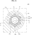
- FIG. 2A is an enlarged schematic plan view of an emitter region of FIG. 1
- FIG. 2B is a schematic cross-sectional view taken along line A-A of FIG. 2A .
- a vertical-cavity surface-emitting laser (VCSEL) 100 includes an emitter 150, a pad 40, and a connector 41.
- the emitter 150 includes a lower mirror 25, an active layer 27, an aperture forming layer 29, and an upper mirror 31.
- the VCSEL 100 may also include a substrate 21, a buffer layer 23, an ohmic contact layer 33, a surface protection layer 35, and an upper insulation layer 39.
- the VCSEL 100 may also include an insulation region 37 by ion implantation, and an isolation region surrounded by the insulation region, and may include oxidation holes.
- the substrate 21 may be a conductive substrate.
- the substrate 21 may be a semiconductor substrate, such as n-type GaAs.
- the substrate 21 may also be a growth substrate for growing semiconductor layers disposed thereon, and may be selected according to the semiconductor layer to be grown thereon.
- the buffer layer 23 may be formed to assist the growth of the semiconductor layers, but in some exemplary embodiments, the buffer layer 23 may be omitted.
- the buffer layer 23 may be, for example, a GaAs layer.
- the lower mirror 25 has a distributed Bragg reflector (DBR) structure, and may include n-type semiconductor layers.
- the lower mirror 25 may be formed by, for example, repeatedly stacking semiconductor layers having different refractive indices.
- the lower mirror 25 may be formed by alternately stacking an AlGaAs layer having a relatively low Al content, and an AlGaAs layer having a relatively high Al content.
- the lower mirror 25 may be formed by alternately stacking an Al 0.15 Ga 0.85 As layer having an Al content of 15%, and an Al 0.85 Ga 0.15 As layer having an Al content of 85%.
- Si may be doped at a concentration of approximately 1 to 3 ⁇ 10 18 /cm 3 .
- the lower mirror 25 may include, for example, 30 or more pairs of semiconductor layers having different refractive indices.
- a thickness of each layer in the lower mirror 25 may be about one-fourth of a wavelength of light.
- the active layer 27 may be disposed on the lower mirror 25, and may contact the lower mirror 25.
- the active layer 27 may have a barrier layer and a well layer, and the well layer may be interposed between the barrier layers.
- the active layer 27, in particular, may have a multi-quantum well structure having a plurality of well layers, and may include, for example, a stacked structure of GaAs/InGaAs/GaAs. Compositions of the barrier layer and the well layer may be varied according to a desired laser wavelength, and the well layer may include, for example, an InAlGaAs-based four-component, three-component, or two-component structure.
- the inventive concepts are not limited thereto, and in some exemplary embodiments, the active layer 27 may include InAlGaN-based or InAlGaP-based semiconductor layers, and in this case, the barrier layer and the well layer may have a nitride-based or phosphide-based composition.
- the well layer in the active layer 27 may be formed of an un-doped layer, and the barrier layer may also be formed of an un-doped layer.
- a thickness of the well layer may be approximately 2 nm to 8 nm, and the thickness of the barrier layer may be approximately in a range of 2 nm to 15 nm.
- the upper mirror 31 is disposed on the active layer 27.
- the upper mirror 31 may have a distributed Bragg reflector (DBR) structure, and may include p-type semiconductor layers.
- the upper mirror 31 may be formed by, for example, repeatedly stacking semiconductor layers having different refractive indices.
- the upper mirror 31 may be formed by alternately stacking an AlGaAs layer having a relatively low Al content and an AlGaAs layer having a relatively high Al content, as in the lower mirror 25.
- the upper mirror 31 may be formed by alternately stacking an Al 0.15 Ga 0.85 As layer having an Al content of 15%, and an Al 0.85 Ga 0.15 As layer having an Al content of 85%.
- C may be doped at a concentration of about 1 to 5 ⁇ 10 18 /cm 3 .
- the upper mirror 31 may include, for example, 20 or more pairs of semiconductor layers having different refractive indices. The number of pairs in the upper mirror 31 may be relatively smaller than that in the lower mirror 25, without being limited thereto. Meanwhile, a thickness of each layer may be set to be about one-fourth of a wavelength of light.
- the aperture forming layer 29 is disposed between the active layer 27 and the upper mirror 31.
- the aperture forming layer 29 may include an oxidation layer 29x and a window layer 29w.
- the window layer 29w is surrounded by the oxidation layer 29x, thereby forming an aperture defining a passage of current.
- the aperture forming layer 29 may be formed of, for example, an AlGaAs layer having a higher Al content than the layers in the upper mirror 31.
- an Al content in the aperture forming layer 29 may be about 90% or more.
- the oxidation layer 29x is formed by oxidizing the AlGaAs layer in a region except the window layer 29w.
- a width of the aperture formed by the oxidation layer 29x, in particular, the width of the window layer 29w is not particularly limited, but in some exemplary embodiments, may be in a range of about 8 ⁇ m to about 12 ⁇ m.
- FIG. 2A shows that the window layer 29w or the aperture has a disk shape, however, the inventive concepts are not limited thereto.
- the window layer 29w may have other shapes, such as a polygonal shape close to the disk. This will be described in more detail with reference to FIGS. 9A through 9D .
- the emitter 150 includes an insulation region 37 formed by ion implantation, and an isolation region surrounded by the insulation region 37. Ions may be implanted into the upper mirror 31, and into the aperture forming layer 29 and the active layer 27. In some exemplary embodiments, ions may further be implanted into some thickness regions of the lower mirror 25.
- the insulation region 37 may improve light efficiency by preventing current from flowing to other regions except for the aperture (e.g., window layer 29w).
- the ohmic contact layer 33 is disposed on the upper mirror 31.
- the ohmic contact layer 33 may form an ohmic contact with the upper mirror 31 in the isolation region surrounded by the insulation region 37.
- the ohmic contact layer 33 may include, for example, Ti, Pt, and Au, and ohmic contact may be formed using a rapid thermal annealing process, for example.
- the ohmic contact layer 33 as shown in FIG. 2A , may include a partial ring-shaped circular portion 33a and protrusions 33b protruding outwardly from the circular portion 33a.
- the surface protection layer 35 protects the upper mirror 31 and the ohmic contact layer 33 during an ion implantation process.
- the surface protection layer 35 may be formed of a light transmissive substance, such as a silicon oxide film or a silicon nitride film.
- the surface protection layer 35 may have a thickness of an integer multiple of one-fourth of a light wavelength.
- the surface protection layer 35 may be formed to have a thickness, which is an integer multiple of about 118 nm.
- the surface protection layer 35 is formed to have a tensile strain, and may be formed at, for example, about 250°C.
- Oxidation holes 29a are formed to expose the aperture forming layer 29.
- the oxidation holes 29a may pass through the upper mirror 31 and the aperture forming layer 29, and further, may pass through the active layer 27 and a portion of the lower mirror 25.
- the oxidation holes 29a may also pass through the surface protection layer 35.
- the oxidation holes 29a may be disposed outside of the ohmic contact layer 33, and in particular, may be disposed between the protrusions 33b. Further, the oxidation holes 29a are formed in the isolation region surrounded by the insulation region 37. The oxidation holes 29a are disposed in the isolation region away from the insulation region 37 formed by ion implantation, and thus, defects generated during ion implantation may be prevented from moving to the aperture while forming the oxidation layer 29x. In addition, since the ohmic contact layer 33 is formed to have the protrusions 33b, the oxidation holes 29a may be disposed closer to one another, thereby reducing the size of the emitter 150.
- the oxidation holes 29a may be formed to have sizes smaller than those of the protrusions 33b, respectively.
- a width of the oxidation hole 29a may be less than that of the protrusion 33b. In this manner, penetration of moisture or the like through the oxidation holes 29a after the oxidation layer is formed may be suppressed.
- a depth of the oxidation holes 29a may be about 3 ⁇ m, and a diameter of the hole may be about 4 ⁇ m.
- the aperture forming layer 29 is oxidized through the oxidation holes 29a, and thus, the oxidation layer 29x and the window layer 29w are defined.
- the upper mirror 31, the active layer 27, and the lower mirror 25 exposed to sidewalls of the oxidation holes 29a may be partially oxidized.
- the upper insulation layer 39 covers the surface protection layer 35 and the oxidation holes 29a.
- the upper mirror 31, the oxidation layer 29x, the active layer 27, and the lower mirror 25 exposed in the oxidation holes 29a are covered with the upper insulation layer 39 to be insulated.
- the upper insulation layer 39 may be formed of a light transmissive substance, such as a silicon oxide film or a silicon nitride film.
- the upper insulation layer 39 may also be formed to have a thickness, which is an integer multiple of one-fourth of a light wavelength.
- the surface protection layer 35 may be formed to have a thickness, about 200 nm, about 300 nm, or about 500 nm.
- the upper insulation layer 39 is formed to have a tensile strain, and may be formed at, for example, 250°C.
- Via holes 39a passing through the upper insulation layer 39 and the surface protection layer 35 may be formed to expose the ohmic contact layer 33.
- the via holes 39a are disposed correspond to the protrusions 33b of the ohmic contact layer 33.
- the via holes 39a may be formed to expose the protrusion 33b and the circular portion 33a together.
- FIG. 2A shows the via holes 39a as having a quadrangular shape, the inventive concepts are not limited thereto, and in some exemplary embodiments, the via holes 39a may have a substantially circular shape, for example.
- the pad 40 and the connector 41 may be disposed on the upper insulation layer 39.
- the pad 40 is a region to which bonding wires may be disposed, and is disposed over a relatively wide region.
- the pad 40 may be disposed, for example, in the insulation region 37 formed by ion implantation, and thus, may reduce parasitic capacitance.
- the connector 41 electrically connects the pad 40 and the ohmic contact layer 33.
- the connector 41 may be connected to the ohmic contact layer 33 through the via holes 39a.
- the connector 41 may have a partial ring-shaped circular portion along the ohmic contact layer 33, and an opening 41a may be provided inside the ring-shaped circular portion to emit a laser beam.
- the pad 40 and the connector 41 may include substantially the same metal material, such as Ti/Pt/Au.
- the pad 40 and the connector 41 may be formed to have a thickness of about at least 2 ⁇ m.
- another pad for example, an n-pad may be formed under the substrate 21.
- the n-pad may be formed of AuGe/Ni/Au(900 ⁇ /300 ⁇ /1000 ⁇ 3000 ⁇ ), for example.
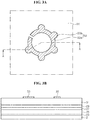
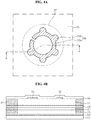
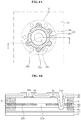
- FIGS. 3A, 3B , 4A, 4B , 5A, 5B , 6A, and 6B are schematic plan views and cross-sectional views illustrating a method of manufacturing a VCSEL according to an exemplary embodiment.
- Each cross-sectional view is a view taken along line A-A of the corresponding plan view.
- layers 23, 25, 27, 29, and 31 are formed on a substrate 21, which may include a semiconductor material, and an ohmic contact layer 33 is formed thereon.
- the substrate 21 may be, for example, an n-type GaAs substrate.
- the semiconductor layers may include a buffer layer 23, a lower mirror 25, an active layer 27, an aperture forming layer 29, and an upper mirror 31.
- the semiconductor layers may be formed using, for example, epitaxial growth techniques, such as metal organic chemical vapor deposition or molecular beam epitaxy.
- the buffer layer 23 may be formed of, for example, a GaAs layer disposed on the substrate 21.
- the lower mirror 25 may be formed on the buffer layer 23, and the active layer 27, the aperture forming layer 29, and the upper mirror 31 may be sequentially formed on the lower mirror 25.
- the lower mirror 25 and the upper mirror 31 may be formed by repeatedly stacking AlGaAs/AlGaAs having different Al compositions, respectively. Since the specific structures of the lower mirror 25, the active layer 27, the aperture forming layer 29 and the upper mirror 31 have been described in detail above, repeated descriptions thereof will be omitted to avoid redundancy.
- the ohmic contact layer 33 is formed on the upper mirror 31.
- the ohmic contact layer 33 may include a partial ring-shaped circular portion 33a and protrusions 33b protruding outwardly from the circular portion 33a.
- the ohmic contact layer 33 may be heat-treated through a rapid thermal annealing process after forming a metal layer using a lift-off technique, for example.
- the metal layer may be formed of, for example, Ti/Pt/Au, which may be formed to have thicknesses of about 300 ⁇ , 300 ⁇ , and 1000 to 3000 ⁇ , respectively. In this manner, an ohmic contact may be formed between the ohmic contact layer 33 and the upper mirror 31 by the thermal annealing process.
- the substrate 21 may have a diameter of, for example, about 10 mm, and multiple ohmic contact layers 33 may be formed in each device region.
- the positive photoresist may be used for a high density array.
- a surface protection layer 35 covering the upper mirror 31 and the ohmic contact layer 33 is formed.
- the surface protection layer 35 protects the surface of the upper mirror 31 during an ion implantation process (e.g., implantation).
- the surface protection layer 35 may be formed of, for example, Si 3 N 4 or SiO 2 , and may have a thickness, which is an integer multiple of one-fourth of a light wavelength.
- the surface protection layer 35 may have a thickness, which is an integer multiple of about 118 nm.
- a photoresist is formed on the surface protection layer 35, and ions are implanted through the upper mirror 31 by the ion implantation process using the photoresist as a mask.
- Hydrogen ions may be implanted, thereby converting an ion implanted region into an insulation region.
- An implant energy of hydrogen ions may be used up to about 350 keV, and the photoresist may be formed to have a thickness, for example about 8 ⁇ m, sufficient to prevent hydrogen ions of this energy.
- the photoresist is formed to cover the ohmic contact layer 33, and thus, ion implantation is performed outside of the ohmic contact layer 33.
- an isolation region may be defined as a circular region by ion implantation, and an insulation region 37 is formed outside thereof.
- the insulation region 37 may be formed up to a partial thickness of the lower mirror 25 as shown in FIG. 4B .
- oxidation holes 29a are formed.
- the oxidation holes 29a may pass through the surface protection layer 35, the upper mirror 31, the aperture forming layer 29, and the active layer 27, and may pass through a partial thickness of the lower mirror 25.
- the oxidation holes 29a are formed in the isolation region surrounded by the insulation region 37, and thus, are spaced apart from the ion implanted region.
- the oxidation holes 29a may be disposed between the protrusions 33b, and may have sizes smaller than those of the protrusions 33b.
- the oxidation holes 29a have a depth of about 3 ⁇ m, a diameter (or width) of about 4 ⁇ m at a side of an inlet, and sidewalls thereof may be inclined at about 80 degrees.
- the shapes of the oxidation holes 29a may vary, which will be described later in more detail with reference to FIGS. 9A through 9D . Since the ohmic contact layer 33 is formed to have the protrusions 33b, the width of the circular portion 33a may be reduced, thereby reducing a distance between the oxidation holes 29a.
- the aperture forming layer 29 exposed through the oxidation holes 29a may be oxidized. Oxidation may be performed at, for example, in a range of 400°C to 430°C, and, by adjusting an Al composition ratio of the aperture forming layer 29, the temperature and composition thereof may be set to exhibit an oxidation rate of 10 times or more as compared to those of the layers in the lower and upper mirrors 25 and 31.
- An oxidation layer 29x is formed in the aperture forming layer 29 by the oxidation process.
- the oxidation layer 29x proceeds to the inside of the aperture forming layer 29 through the exposed aperture forming layer 29 in an inner wall of the oxidation holes 29a. Accordingly, a window layer 29w (aperture) is formed under a region surrounded by the ohmic contact layer 33. Meanwhile, as shown in FIG. 5B , a portion of the oxidation layer 29x may also be formed in the insulation region 37.
- the oxidation proceeds at a relatively high temperature of about 400 °C to about 430 °C, defects formed in the insulation region 37 may move by ion implantation. At this time, since the oxidation hole 29a are disposed in the isolation region surrounded by the insulation region 37, the defects may be prevented from moving toward the window layer 29w.
- an upper insulation layer 39 is formed on the surface protection layer 35.
- the upper insulation layer 39 may be formed of a light transmissive substance, and may be formed of, for example, Si 3 N 4 or SiO 2 .
- the upper insulation layer 39 covers sidewalls and a bottom of the oxidation holes 29a to insulate the semiconductor layers exposed in the oxidation holes 29a.
- via holes 39a exposing the ohmic contact layer 33 may be formed by patterning the upper insulation layer 39 and the surface protection layer 35.
- the via holes 39a may be formed to correspond to the protrusions 33b of the ohmic contact layer 33, as shown in FIG. 6A .
- a device isolation region for example, a scribing line for dividing the substrate 21 into a plurality of device regions may be formed together.
- the scribing line is formed by etching the surface protection layer 35 and the upper insulation layer 39, such that the upper insulation layer 39 may be prevented from being peeled off during a scribing process to divide devices in subsequent processes.
- a pad 40 and a connector 41 are formed, as shown in FIG. 1 .
- the pad 40 and the connector 41 may be formed using a lift off technique, for example, and may be formed of, for example, Ti/Pt/Au.
- an n-pad may be further formed on the lower surface of the substrate 21 before dividing the substrate 21.
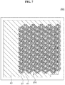
- FIG. 7 is a schematic plan view of a VCSEL according to another exemplary embodiment
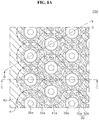
- FIG. 8A is an enlarged schematic plan view of a portion of an emitter array of FIG. 7
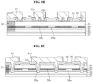
- FIG. 8B is a schematic cross-sectional view taken along line B-B of FIG. 8A
- FIG. 8C is a schematic cross-sectional view taken along line C-C of FIG. 8A .
- a VCSEL 200 according to the illustrated exemplary embodiment is generally similar to the VCSEL 100 described with reference to FIG. 1 , FIG. 2A , and FIG. 2B , except that the VCSEL 200 includes a plurality of emitter arrays 250, and, accordingly, the shape of the pad 40 may be modified. As such, repeated descriptions of substantially the same elements forming the VCSEL will be omitted to avoid redundancy.
- the emitters may be disposed in substantially a honeycomb shape on the substrate 21.
- An emitter array region 250 may be surrounded by an insulation region 37 by ion implantation, and the pad 40 is disposed in the insulation region 37.
- the pad 40 may be formed on one side of the substrate 21 adjacent to the array region 250.
- the insulation region 37 may not be formed in the emitter array region 250 by ion implantation. More particularly, the ion implantation is performed only outside of a boundary line surrounding an outer side of the emitter array region 250 to form the insulation region 37.
- Each emitter includes a lower mirror 25, an active layer 27, an aperture forming layer 29, and a upper mirror 31, as those described with reference to FIG. 1 , FIG. 2A , and FIG. 2B .
- the aperture forming layer 29 also includes an oxidation layer 29x and a window layer 29w, such that current flow is limited to the window layer 29w.
- a basic structure of each emitter is substantially the same as the emitter 150 described above, except for the insulation region 37 by ion implantation.
- an ohmic contact layer 33 may be formed in each emitter.
- the ohmic contact layer 33 may include a circular portion 33a and protrusions 33b having a partial ring shape.
- oxidation holes 29a are disposed between the protrusions 33b, and via holes 39a are formed to correspond to the protrusions 33b.
- the oxidation holes 29a and the via holes 39a formed in each emitter are substantially the same as those formed in the emitter 150 described above.
- sizes of the oxidation holes 29a may be smaller than those of the protrusions 33b, thereby improving reliability of the device.
- the oxidation holes 29a are formed in an isolation region surrounded by the insulation region 37 formed by ion implantation. As such, defects may be prevented from moving near the window layer 29w during the oxidation process, thereby improving the reliability of the device.
- a connector 41 connecting the pad 40 and the ohmic contact layers 33 may be connected to each emitter through the via holes 39a.
- Each of the emitters may be connected in parallel.
- the connector 41 of FIG. 1 is shown as having a partial ring shape, it is difficult to form the connector 41 to have the partial ring shape when the connector 41 is connected to a plurality of emitters.
- the connector 41 according to the illustrated exemplary embodiment may have a mesh shape forming circular openings 41a, as shown in FIG. 8A .
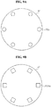
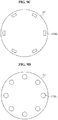
- FIG. 9A is a schematic plan view illustrating oxidation holes 29a for forming an oxidation layer according to an exemplary embodiment
- FIGS. 9B through 9D are schematic plan views illustrating various modifications of oxidation holes for forming an oxidation layer according to exemplary embodiments.
- the oxidation holes 29a are formed in an isolation region surrounded by an insulation region 37 by ion implantation.
- the oxidation holes 29a may be formed to have substantially a circular or elliptical shape.
- six oxidation holes 29a may be formed, and an aperture forming layer 29 may be oxidized to form an oxidation layer 29x, and a window layer 29w is formed in the isolation region by the oxidation layers 29x.
- the window layer 29w may have substantially a circular shape.
- a shape and arrangement of the oxidation holes 29a may be variously modified.
- the oxidation holes 129a may have substantially a square or rectangular shape, and be disposed at locations corresponding to each vertex of the regular hexagon.
- the oxidation holes 129b may have substantially a quadrangular shape, a side close to a center of the isolation region may curved.
- eight oxidation holes 129c may be disposed at locations corresponding to each vertex of the regular octagon.
- the circular or elliptical oxidation holes 29a may be easily formed using photo and etching techniques, and may also increase the stability of an upper insulation layer 39 or a connector 41 formed thereon.
- the inventive concepts are not limit thereto, and in some exemplary embodiments, the oxidation holes 29a may have substantially a quadrangular shape or another shape as described above.
Landscapes
- Physics & Mathematics (AREA)
- Condensed Matter Physics & Semiconductors (AREA)
- General Physics & Mathematics (AREA)
- Electromagnetism (AREA)
- Optics & Photonics (AREA)
- Geometry (AREA)
- Semiconductor Lasers (AREA)
Abstract
Description
- Exemplary embodiments of the invention relate to a highly reliable vertical-cavity surface-emitting laser.
- A vertical-cavity surface-emitting laser (VCSEL) is a laser that emits a laser beam in a vertical direction from a substrate surface.
- A typical VCSEL includes an active layer disposed between mirrors. Electrons and holes injected through the mirrors generate light from the active layer, and a laser is generated and emitted through resonance by the mirrors.
- Current flowing perpendicular to the VCSEL needs to be limited to a small region. As such, methods using etching and oxidation have been used to form a conventional VCSEL. For example, an isolated post is formed by etching mirror layers and the active layer to form a trench having a ring shape, such that current may be concentrated in an aperture of a small region by forming an oxidation layer using the trench.
- In this case, however, etching a wide area to form the ring-shaped trench may increase manufacturing complexity. Moreover, when forming a pad electrode, connection between the pad and an emitter passes through the trench, which may increase the risk of electrical disconnection and lower the process yield. In addition, a trench having a large area is formed around the emitter, and thus, the emitter's reliability is also adversely affected by a surface defect.
- Exemplary embodiments of the invention provide high reliable vertical-cavity surface-emitting lasers (VCSELs).
- Exemplary embodiments of the invention provide vertical-cavity surface-emitting lasers (VCSELs) capable of preventing the occurrence of electrical disconnection due to a trench.
- Exemplary embodiments also provide VCSELs capable of preventing the performance of an emitter from being degraded by defects.
- A vertical-cavity surface-emitting laser (VCSEL) according to an exemplary embodiment includes a lower mirror, an upper mirror having an insulation region including implanted ions and an isolation region surrounded by the insulation region, an active layer interposed between the lower mirror and the upper mirror, an aperture forming layer interposed between the upper mirror and the active layer, and including an oxidation layer and a window layer surrounded by the oxidation layer, and a plurality of oxidation holes disposed in the isolation region and passing through the upper mirror and the aperture forming layer.
- A vertical-cavity surface-emitting laser (VCSEL) according to another exemplary embodiment includes a lower mirror, an upper mirror having an insulation region including implanted ions and an isolation region surrounded by the insulation region, an emitter array including a plurality of emitters disposed in the isolation region, an active layer interposed between the lower mirror and the upper mirror, an aperture forming layer interposed between the upper mirror and the active layer, and including an oxidation layer and a window layer surrounded by the oxidation layer, and a plurality of oxidation holes disposed in the isolation region and passing through the upper mirror and the aperture forming layer, each oxidation hole being disposed to correspond to each emitter of the emitter array.
- According to exemplary embodiments, it is possible to prevent the occurrence of electrical disconnection, by forming an insulation region by ion implantation. Furthermore, by placing the oxidation holes in the isolation region, it is possible to prevent defects formed during ion implantation from moving into an emitter, thereby providing a highly reliable VCSEL.
-
-
FIG. 1 is a schematic plan view of a VCSEL according to an exemplary embodiment. -
FIG. 2A is an enlarged schematic plan view of an emitter region ofFIG. 1 . -
FIG. 2B is a schematic cross-sectional view taken along line A-A ofFIG. 2A . -
FIGS. 3A, 3B ,4A, 4B ,5A, 5B ,6A, and 6B are schematic plan views and cross-sectional views illustrating a method of manufacturing a VCSEL according to an exemplary embodiment. -
FIG. 7 is a schematic plan view of a VCSEL according to another exemplary embodiment. -
FIG. 8A is an enlarged schematic plan view of a portion of an emitter array ofFIG. 7 . -
FIG. 8B is a schematic cross-sectional view taken along line B-B ofFIG. 8A . -
FIG. 8C is a schematic cross-sectional view taken along line C-C ofFIG. 8A . -
FIG. 9A is a schematic plan view illustrating oxidation holes for forming an oxidation layer according to an exemplary embodiment. -
FIGS. 9B ,9C, and 9D are schematic plan views illustrating oxidation holes for forming an oxidation layer according to exemplary embodiments. - Hereinafter, exemplary embodiments of the present disclosure will be described in detail with reference to the accompanying drawings. The following embodiments are provided by way of example so as to fully convey the spirit of the present disclosure to those skilled in the art to which the present disclosure pertains. Accordingly, the present disclosure is not limited to the embodiments disclosed herein and can also be implemented in different forms. In the drawings, widths, lengths, thicknesses, and the like of elements can be exaggerated for clarity and descriptive purposes. When an element or layer is referred to as being "disposed above" or "disposed on" another element or layer, it can be directly "disposed above" or "disposed on" the other element or layer or intervening elements or layers can be present. Throughout the specification, like reference numerals denote like elements having the same or similar functions.
- A vertical-cavity surface-emitting laser (VCSEL) according to an exemplary embodiment includes a lower mirror, an upper mirror having an insulation region including implanted ions and an isolation region surrounded by the insulation region, an active layer interposed between the lower mirror and the upper mirror, an aperture forming layer interposed between the upper mirror and the active layer, and including an oxidation layer and a window layer surrounded by the oxidation layer, and a plurality of oxidation holes disposed in the isolation region and passing through the upper mirror and the aperture forming layer.
- By placing the oxidation holes in the isolation region, it is possible to prevent defects formed during ion implantation from moving near the window layer, thereby providing a highly reliable VCSEL.
- The insulation region may extend from the upper mirror to a portion of the lower mirror.
- The VCSEL may further include an ohmic contact layer disposed on the upper mirror, in which the ohmic contact layer may include a circular portion and protrusions protruding outwardly from the of the circular portion.
- The circular portion may have a partially incised ring-shape.
- The oxidation holes may be disposed between the protrusions.
- The oxidation holes may have smaller widths than those of the protrusions, respectively.
- The VCSEL may further include a surface protection layer covering the ohmic contact layer and the upper mirror, and an upper insulation layer disposed on the surface protection layer and covering the oxidation holes, in which the oxidation holes may pass through the surface protection layer.
- The VCSEL may further include a plurality of via holes passing through the upper insulation layer and the surface protection layer and exposing the ohmic contact layer, in which the via holes may be disposed to correspond to the protrusions.
- The VCSEL may further include a pad and a connector disposed on the upper insulation layer, in which the pad may be disposed in the insulation region, and the connector may extend from the pad and electrically connect the pad and the ohmic contact layer through the via holes.
- The oxidation holes may have substantially a circular or a quadrangular shape.
- According to another embodiment of the present disclosure, a VCSEL including an emitter array is provided. The VCSEL includes a lower mirror, an upper mirror having an insulation region including implanted ions and an isolation region surrounded by the insulation region, an emitter array including a plurality of emitters disposed in the isolation region, an active layer interposed between the lower mirror and the upper mirror, an aperture forming layer interposed between the upper mirror and the active layer, and including an oxidation layer and a window layer surrounded by the oxidation layer, and a plurality of oxidation holes disposed in the isolation region and passing through the upper mirror and the aperture forming layer, each oxidation hole being disposed to correspond to each emitter of the emitter array.
- The insulation region may extend from the upper mirror to a portion of the lower mirror.
- The VCSEL may further include ohmic contact layers disposed on the upper mirror to correspond to each emitter of the emitter array, respectively, in which each ohmic contact layer may have a circular portion and protrusions protruding outwardly from the circular portion, and the oxidation holes may be disposed between the protrusions. The circular portion may have a partially incised ring-shape. The oxidation holes may have smaller widths than those of the protrusions, respectively.
- The VCSEL may further include a surface protection layer covering the ohmic contact layer and the upper mirror, and an upper insulation layer disposed on the surface protection layer and covering the oxidation holes, in which the oxidation holes may pass through the surface protection layer.
- The VCSEL may further include a plurality of via holes passing through the upper insulation layer and the surface protection layer and exposing the ohmic contact layer, in which the via holes may be disposed to correspond to the protrusions.
- The VCSEL may further include a pad and a connector disposed on the upper insulation layer, in which the pad may be disposed in the insulation region, and the connector may extend from the pad and electrically connect the pad and the ohmic contact layer through the via holes.
- The connector may have a mesh shape including circular openings corresponding to each emitter.
- The oxidation holes may have substantially a circular or a quadrangular shape.
- Hereinafter, embodiments of the present disclosure will be described in detail with reference to the accompanying drawings.
-
FIG. 1 is a schematic plan view of a VCSEL according to an exemplary embodiment,FIG. 2A is an enlarged schematic plan view of an emitter region ofFIG. 1 , andFIG. 2B is a schematic cross-sectional view taken along line A-A ofFIG. 2A . - Referring to
FIG. 1 ,FIG. 2A , andFIG. 2B , a vertical-cavity surface-emitting laser (VCSEL) 100 according to an exemplary embodiment includes anemitter 150, apad 40, and aconnector 41. Theemitter 150 includes alower mirror 25, anactive layer 27, anaperture forming layer 29, and anupper mirror 31. TheVCSEL 100 may also include asubstrate 21, abuffer layer 23, anohmic contact layer 33, asurface protection layer 35, and anupper insulation layer 39. TheVCSEL 100 may also include aninsulation region 37 by ion implantation, and an isolation region surrounded by the insulation region, and may include oxidation holes. - The
substrate 21 may be a conductive substrate. For example, thesubstrate 21 may be a semiconductor substrate, such as n-type GaAs. Thesubstrate 21 may also be a growth substrate for growing semiconductor layers disposed thereon, and may be selected according to the semiconductor layer to be grown thereon. - The
buffer layer 23 may be formed to assist the growth of the semiconductor layers, but in some exemplary embodiments, thebuffer layer 23 may be omitted. When thesubstrate 21 is a GaAs substrate, thebuffer layer 23 may be, for example, a GaAs layer. - The
lower mirror 25 has a distributed Bragg reflector (DBR) structure, and may include n-type semiconductor layers. Thelower mirror 25 may be formed by, for example, repeatedly stacking semiconductor layers having different refractive indices. For example, thelower mirror 25 may be formed by alternately stacking an AlGaAs layer having a relatively low Al content, and an AlGaAs layer having a relatively high Al content. In particular, thelower mirror 25 may be formed by alternately stacking an Al0.15Ga0.85As layer having an Al content of 15%, and an Al0.85Ga0.15As layer having an Al content of 85%. As an n-type impurity, Si may be doped at a concentration of approximately 1 to 3×10¹⁸/cm3. Thelower mirror 25 may include, for example, 30 or more pairs of semiconductor layers having different refractive indices. A thickness of each layer in thelower mirror 25 may be about one-fourth of a wavelength of light. - The
active layer 27 may be disposed on thelower mirror 25, and may contact thelower mirror 25. Theactive layer 27 may have a barrier layer and a well layer, and the well layer may be interposed between the barrier layers. Theactive layer 27, in particular, may have a multi-quantum well structure having a plurality of well layers, and may include, for example, a stacked structure of GaAs/InGaAs/GaAs. Compositions of the barrier layer and the well layer may be varied according to a desired laser wavelength, and the well layer may include, for example, an InAlGaAs-based four-component, three-component, or two-component structure. However, the inventive concepts are not limited thereto, and in some exemplary embodiments, theactive layer 27 may include InAlGaN-based or InAlGaP-based semiconductor layers, and in this case, the barrier layer and the well layer may have a nitride-based or phosphide-based composition. - The well layer in the
active layer 27 may be formed of an un-doped layer, and the barrier layer may also be formed of an un-doped layer. A thickness of the well layer may be approximately 2 nm to 8 nm, and the thickness of the barrier layer may be approximately in a range of 2 nm to 15 nm. - The
upper mirror 31 is disposed on theactive layer 27. Theupper mirror 31 may have a distributed Bragg reflector (DBR) structure, and may include p-type semiconductor layers. Theupper mirror 31 may be formed by, for example, repeatedly stacking semiconductor layers having different refractive indices. For example, theupper mirror 31 may be formed by alternately stacking an AlGaAs layer having a relatively low Al content and an AlGaAs layer having a relatively high Al content, as in thelower mirror 25. In particular, theupper mirror 31 may be formed by alternately stacking an Al0.15Ga0.85As layer having an Al content of 15%, and an Al0.85Ga0.15As layer having an Al content of 85%. As a p-type impurity, for example, C may be doped at a concentration of about 1 to 5×10¹⁸/cm3. Theupper mirror 31 may include, for example, 20 or more pairs of semiconductor layers having different refractive indices. The number of pairs in theupper mirror 31 may be relatively smaller than that in thelower mirror 25, without being limited thereto. Meanwhile, a thickness of each layer may be set to be about one-fourth of a wavelength of light. - The
aperture forming layer 29 is disposed between theactive layer 27 and theupper mirror 31. Theaperture forming layer 29 may include anoxidation layer 29x and awindow layer 29w. Thewindow layer 29w is surrounded by theoxidation layer 29x, thereby forming an aperture defining a passage of current. Theaperture forming layer 29 may be formed of, for example, an AlGaAs layer having a higher Al content than the layers in theupper mirror 31. For example, an Al content in theaperture forming layer 29 may be about 90% or more. Theoxidation layer 29x is formed by oxidizing the AlGaAs layer in a region except thewindow layer 29w. - A width of the aperture formed by the
oxidation layer 29x, in particular, the width of thewindow layer 29w is not particularly limited, but in some exemplary embodiments, may be in a range of about 8 µm to about 12 µm. - Although
FIG. 2A shows that thewindow layer 29w or the aperture has a disk shape, however, the inventive concepts are not limited thereto. In some exemplary embodiments, thewindow layer 29w may have other shapes, such as a polygonal shape close to the disk. This will be described in more detail with reference toFIGS. 9A through 9D . - The
emitter 150 includes aninsulation region 37 formed by ion implantation, and an isolation region surrounded by theinsulation region 37. Ions may be implanted into theupper mirror 31, and into theaperture forming layer 29 and theactive layer 27. In some exemplary embodiments, ions may further be implanted into some thickness regions of thelower mirror 25. - The
insulation region 37 may improve light efficiency by preventing current from flowing to other regions except for the aperture (e.g.,window layer 29w). - The
ohmic contact layer 33 is disposed on theupper mirror 31. In particular, theohmic contact layer 33 may form an ohmic contact with theupper mirror 31 in the isolation region surrounded by theinsulation region 37. Theohmic contact layer 33 may include, for example, Ti, Pt, and Au, and ohmic contact may be formed using a rapid thermal annealing process, for example. Theohmic contact layer 33, as shown inFIG. 2A , may include a partial ring-shapedcircular portion 33a andprotrusions 33b protruding outwardly from thecircular portion 33a. - The
surface protection layer 35 protects theupper mirror 31 and theohmic contact layer 33 during an ion implantation process. Thesurface protection layer 35 may be formed of a light transmissive substance, such as a silicon oxide film or a silicon nitride film. Thesurface protection layer 35 may have a thickness of an integer multiple of one-fourth of a light wavelength. For example, when thesurface protection layer 35 is formed of Si3N4, thesurface protection layer 35 may be formed to have a thickness, which is an integer multiple of about 118 nm. In addition, thesurface protection layer 35 is formed to have a tensile strain, and may be formed at, for example, about 250°C. -
Oxidation holes 29a are formed to expose theaperture forming layer 29. In this case, theoxidation holes 29a may pass through theupper mirror 31 and theaperture forming layer 29, and further, may pass through theactive layer 27 and a portion of thelower mirror 25. Theoxidation holes 29a may also pass through thesurface protection layer 35. - The
oxidation holes 29a may be disposed outside of theohmic contact layer 33, and in particular, may be disposed between theprotrusions 33b. Further, theoxidation holes 29a are formed in the isolation region surrounded by theinsulation region 37. The oxidation holes 29a are disposed in the isolation region away from theinsulation region 37 formed by ion implantation, and thus, defects generated during ion implantation may be prevented from moving to the aperture while forming theoxidation layer 29x. In addition, since theohmic contact layer 33 is formed to have theprotrusions 33b, theoxidation holes 29a may be disposed closer to one another, thereby reducing the size of theemitter 150. - In addition, the
oxidation holes 29a may be formed to have sizes smaller than those of theprotrusions 33b, respectively. For example, a width of theoxidation hole 29a may be less than that of theprotrusion 33b. In this manner, penetration of moisture or the like through theoxidation holes 29a after the oxidation layer is formed may be suppressed. For example, a depth of theoxidation holes 29a may be about 3 µm, and a diameter of the hole may be about 4 µm. - The
aperture forming layer 29 is oxidized through theoxidation holes 29a, and thus, theoxidation layer 29x and thewindow layer 29w are defined. In this case, theupper mirror 31, theactive layer 27, and thelower mirror 25 exposed to sidewalls of theoxidation holes 29a may be partially oxidized. - The
upper insulation layer 39 covers thesurface protection layer 35 and theoxidation holes 29a. Theupper mirror 31, theoxidation layer 29x, theactive layer 27, and thelower mirror 25 exposed in theoxidation holes 29a are covered with theupper insulation layer 39 to be insulated. Theupper insulation layer 39 may be formed of a light transmissive substance, such as a silicon oxide film or a silicon nitride film. Theupper insulation layer 39 may also be formed to have a thickness, which is an integer multiple of one-fourth of a light wavelength. For example, when theupper insulation layer 39 is formed of Si3N4, thesurface protection layer 35 may be formed to have a thickness, about 200 nm, about 300 nm, or about 500 nm. In addition, theupper insulation layer 39 is formed to have a tensile strain, and may be formed at, for example, 250°C. - Via
holes 39a passing through theupper insulation layer 39 and thesurface protection layer 35 may be formed to expose theohmic contact layer 33. The via holes 39a are disposed correspond to theprotrusions 33b of theohmic contact layer 33. As shown inFIG. 2A , the viaholes 39a may be formed to expose theprotrusion 33b and thecircular portion 33a together. AlthoughFIG. 2A shows the viaholes 39a as having a quadrangular shape, the inventive concepts are not limited thereto, and in some exemplary embodiments, the viaholes 39a may have a substantially circular shape, for example. - The
pad 40 and theconnector 41 may be disposed on theupper insulation layer 39. Thepad 40 is a region to which bonding wires may be disposed, and is disposed over a relatively wide region. Thepad 40 may be disposed, for example, in theinsulation region 37 formed by ion implantation, and thus, may reduce parasitic capacitance. - The
connector 41 electrically connects thepad 40 and theohmic contact layer 33. Theconnector 41 may be connected to theohmic contact layer 33 through the viaholes 39a. Theconnector 41 may have a partial ring-shaped circular portion along theohmic contact layer 33, and anopening 41a may be provided inside the ring-shaped circular portion to emit a laser beam. - The
pad 40 and theconnector 41 may include substantially the same metal material, such as Ti/Pt/Au. Thepad 40 and theconnector 41 may be formed to have a thickness of about at least 2 µm. - In some exemplary embodiments, another pad, for example, an n-pad may be formed under the
substrate 21. When thesubstrate 21 is a GaAs substrate, the n-pad may be formed of AuGe/Ni/Au(900Å/300Å/1000∼3000Å), for example. -
FIGS. 3A, 3B ,4A, 4B ,5A, 5B ,6A, and 6B are schematic plan views and cross-sectional views illustrating a method of manufacturing a VCSEL according to an exemplary embodiment. Each cross-sectional view is a view taken along line A-A of the corresponding plan view. - Referring to
FIG. 3A and FIG. 3B , layers 23, 25, 27, 29, and 31 are formed on asubstrate 21, which may include a semiconductor material, and anohmic contact layer 33 is formed thereon. - The
substrate 21 may be, for example, an n-type GaAs substrate. The semiconductor layers may include abuffer layer 23, alower mirror 25, anactive layer 27, anaperture forming layer 29, and anupper mirror 31. The semiconductor layers may be formed using, for example, epitaxial growth techniques, such as metal organic chemical vapor deposition or molecular beam epitaxy. - The
buffer layer 23 may be formed of, for example, a GaAs layer disposed on thesubstrate 21. Thelower mirror 25 may be formed on thebuffer layer 23, and theactive layer 27, theaperture forming layer 29, and theupper mirror 31 may be sequentially formed on thelower mirror 25. Thelower mirror 25 and theupper mirror 31 may be formed by repeatedly stacking AlGaAs/AlGaAs having different Al compositions, respectively. Since the specific structures of thelower mirror 25, theactive layer 27, theaperture forming layer 29 and theupper mirror 31 have been described in detail above, repeated descriptions thereof will be omitted to avoid redundancy. - The
ohmic contact layer 33 is formed on theupper mirror 31. Theohmic contact layer 33 may include a partial ring-shapedcircular portion 33a andprotrusions 33b protruding outwardly from thecircular portion 33a. Theohmic contact layer 33 may be heat-treated through a rapid thermal annealing process after forming a metal layer using a lift-off technique, for example. The metal layer may be formed of, for example, Ti/Pt/Au, which may be formed to have thicknesses of about 300 Å, 300 Å, and 1000 to 3000 Å, respectively. In this manner, an ohmic contact may be formed between theohmic contact layer 33 and theupper mirror 31 by the thermal annealing process. - In the illustrated exemplary embodiment, although a single
ohmic contact layer 33 is described as being formed on thesubstrate 21, in some exemplary embodiments, thesubstrate 21 may have a diameter of, for example, about 10 mm, and multiple ohmic contact layers 33 may be formed in each device region. - While a negative photoresist or a positive photoresist, as a mask, may be used to form the
ohmic contact layer 33, in some exemplary embodiments, the positive photoresist may be used for a high density array. - Referring to
FIG. 4A and FIG. 4B , asurface protection layer 35 covering theupper mirror 31 and theohmic contact layer 33 is formed. Thesurface protection layer 35 protects the surface of theupper mirror 31 during an ion implantation process (e.g., implantation). - The
surface protection layer 35 may be formed of, for example, Si3N4 or SiO2, and may have a thickness, which is an integer multiple of one-fourth of a light wavelength. For example, when thesurface protection layer 35 is formed of Si3N4, thesurface protection layer 35 may have a thickness, which is an integer multiple of about 118 nm. - Next, a photoresist is formed on the
surface protection layer 35, and ions are implanted through theupper mirror 31 by the ion implantation process using the photoresist as a mask. Hydrogen ions may be implanted, thereby converting an ion implanted region into an insulation region. An implant energy of hydrogen ions may be used up to about 350 keV, and the photoresist may be formed to have a thickness, for example about 8 µm, sufficient to prevent hydrogen ions of this energy. - The photoresist is formed to cover the
ohmic contact layer 33, and thus, ion implantation is performed outside of theohmic contact layer 33. As shown inFIG. 4A , an isolation region may be defined as a circular region by ion implantation, and aninsulation region 37 is formed outside thereof. Theinsulation region 37 may be formed up to a partial thickness of thelower mirror 25 as shown inFIG. 4B . After the ion implantation is complete, the photoresist is removed. - Referring to
FIG. 5A and FIG. 5B ,oxidation holes 29a are formed. Theoxidation holes 29a may pass through thesurface protection layer 35, theupper mirror 31, theaperture forming layer 29, and theactive layer 27, and may pass through a partial thickness of thelower mirror 25. - In addition, the
oxidation holes 29a are formed in the isolation region surrounded by theinsulation region 37, and thus, are spaced apart from the ion implanted region. - The
oxidation holes 29a may be disposed between theprotrusions 33b, and may have sizes smaller than those of theprotrusions 33b. The oxidation holes 29a have a depth of about 3 µm, a diameter (or width) of about 4 µm at a side of an inlet, and sidewalls thereof may be inclined at about 80 degrees. The shapes of theoxidation holes 29a may vary, which will be described later in more detail with reference toFIGS. 9A through 9D . Since theohmic contact layer 33 is formed to have theprotrusions 33b, the width of thecircular portion 33a may be reduced, thereby reducing a distance between theoxidation holes 29a. - Subsequently, the
aperture forming layer 29 exposed through theoxidation holes 29a may be oxidized. Oxidation may be performed at, for example, in a range of 400°C to 430°C, and, by adjusting an Al composition ratio of theaperture forming layer 29, the temperature and composition thereof may be set to exhibit an oxidation rate of 10 times or more as compared to those of the layers in the lower andupper mirrors - An
oxidation layer 29x is formed in theaperture forming layer 29 by the oxidation process. Theoxidation layer 29x proceeds to the inside of theaperture forming layer 29 through the exposedaperture forming layer 29 in an inner wall of theoxidation holes 29a. Accordingly, awindow layer 29w (aperture) is formed under a region surrounded by theohmic contact layer 33. Meanwhile, as shown inFIG. 5B , a portion of theoxidation layer 29x may also be formed in theinsulation region 37. - Since the oxidation proceeds at a relatively high temperature of about 400 °C to about 430 °C, defects formed in the
insulation region 37 may move by ion implantation. At this time, since theoxidation hole 29a are disposed in the isolation region surrounded by theinsulation region 37, the defects may be prevented from moving toward thewindow layer 29w. - Referring to
FIG. 6A and FIG. 6B , anupper insulation layer 39 is formed on thesurface protection layer 35. Theupper insulation layer 39 may be formed of a light transmissive substance, and may be formed of, for example, Si3N4 or SiO2. Theupper insulation layer 39 covers sidewalls and a bottom of theoxidation holes 29a to insulate the semiconductor layers exposed in theoxidation holes 29a. - Meanwhile, via
holes 39a exposing theohmic contact layer 33 may be formed by patterning theupper insulation layer 39 and thesurface protection layer 35. The viaholes 39a may be formed to correspond to theprotrusions 33b of theohmic contact layer 33, as shown inFIG. 6A . - In some exemplary embodiments, when the via
holes 39a are formed, a device isolation region, for example, a scribing line for dividing thesubstrate 21 into a plurality of device regions may be formed together. The scribing line is formed by etching thesurface protection layer 35 and theupper insulation layer 39, such that theupper insulation layer 39 may be prevented from being peeled off during a scribing process to divide devices in subsequent processes. - Subsequently, a
pad 40 and aconnector 41 are formed, as shown inFIG. 1 . Thepad 40 and theconnector 41 may be formed using a lift off technique, for example, and may be formed of, for example, Ti/Pt/Au. - Thereafter, the structure is divided into individual devices along the scribing line, thereby completing the VCSEL of
FIG. 1 . In some exemplary embodiments, an n-pad may be further formed on the lower surface of thesubstrate 21 before dividing thesubstrate 21. -
FIG. 7 is a schematic plan view of a VCSEL according to another exemplary embodiment,FIG. 8A is an enlarged schematic plan view of a portion of an emitter array ofFIG. 7 ,FIG. 8B is a schematic cross-sectional view taken along line B-B ofFIG. 8A , andFIG. 8C is a schematic cross-sectional view taken along line C-C ofFIG. 8A . - Referring to
FIG. 7 ,FIG. 8A ,FIG. 8B, and FIG. 8C , aVCSEL 200 according to the illustrated exemplary embodiment is generally similar to theVCSEL 100 described with reference toFIG. 1 ,FIG. 2A , andFIG. 2B , except that theVCSEL 200 includes a plurality ofemitter arrays 250, and, accordingly, the shape of thepad 40 may be modified. As such, repeated descriptions of substantially the same elements forming the VCSEL will be omitted to avoid redundancy. - The emitters may be disposed in substantially a honeycomb shape on the
substrate 21. Anemitter array region 250 may be surrounded by aninsulation region 37 by ion implantation, and thepad 40 is disposed in theinsulation region 37. Thepad 40 may be formed on one side of thesubstrate 21 adjacent to thearray region 250. - As shown in
FIG. 8A , although lines indicating boundary regions of ion implantation are shown in each emitter region, since the lines in theemitter array region 250 overlap with each other, theinsulation region 37 may not be formed in theemitter array region 250 by ion implantation. More particularly, the ion implantation is performed only outside of a boundary line surrounding an outer side of theemitter array region 250 to form theinsulation region 37. - Each emitter includes a
lower mirror 25, anactive layer 27, anaperture forming layer 29, and aupper mirror 31, as those described with reference toFIG. 1 ,FIG. 2A , andFIG. 2B . Theaperture forming layer 29 also includes anoxidation layer 29x and awindow layer 29w, such that current flow is limited to thewindow layer 29w. A basic structure of each emitter is substantially the same as theemitter 150 described above, except for theinsulation region 37 by ion implantation. - In addition, an
ohmic contact layer 33 may be formed in each emitter. As described above, theohmic contact layer 33 may include acircular portion 33a andprotrusions 33b having a partial ring shape. Further, in each emitter region,oxidation holes 29a are disposed between theprotrusions 33b, and viaholes 39a are formed to correspond to theprotrusions 33b. The oxidation holes 29a and the viaholes 39a formed in each emitter are substantially the same as those formed in theemitter 150 described above. In particular, by forming theoxidation holes 29a separately in each emitter, sizes of theoxidation holes 29a may be smaller than those of theprotrusions 33b, thereby improving reliability of the device. Further, theoxidation holes 29a are formed in an isolation region surrounded by theinsulation region 37 formed by ion implantation. As such, defects may be prevented from moving near thewindow layer 29w during the oxidation process, thereby improving the reliability of the device. - Meanwhile, a
connector 41 connecting thepad 40 and the ohmic contact layers 33 may be connected to each emitter through the viaholes 39a. Each of the emitters may be connected in parallel. Although theconnector 41 ofFIG. 1 is shown as having a partial ring shape, it is difficult to form theconnector 41 to have the partial ring shape when theconnector 41 is connected to a plurality of emitters. As such, theconnector 41 according to the illustrated exemplary embodiment may have a mesh shape formingcircular openings 41a, as shown inFIG. 8A . - Since a manufacturing method of the
VCSEL 200 having the emitter array is substantially similar to that of theVCSEL 100 described above, repeated descriptions thereof will be omitted. -
FIG. 9A is a schematic plan view illustratingoxidation holes 29a for forming an oxidation layer according to an exemplary embodiment, andFIGS. 9B through 9D are schematic plan views illustrating various modifications of oxidation holes for forming an oxidation layer according to exemplary embodiments. - Referring to
FIG. 9A , theoxidation holes 29a are formed in an isolation region surrounded by aninsulation region 37 by ion implantation. The oxidation holes 29a according to the illustrated exemplary embodiment may be formed to have substantially a circular or elliptical shape. In particular, sixoxidation holes 29a may be formed, and anaperture forming layer 29 may be oxidized to form anoxidation layer 29x, and awindow layer 29w is formed in the isolation region by theoxidation layers 29x. Thewindow layer 29w may have substantially a circular shape. - A shape and arrangement of the
oxidation holes 29a may be variously modified. For example, as illustrated inFIG. 9B , theoxidation holes 129a may have substantially a square or rectangular shape, and be disposed at locations corresponding to each vertex of the regular hexagon. In addition, as illustrated inFIG. 9C , although theoxidation holes 129b may have substantially a quadrangular shape, a side close to a center of the isolation region may curved. In addition, as illustrated inFIG. 9D , eightoxidation holes 129c may be disposed at locations corresponding to each vertex of the regular octagon. - The circular or
elliptical oxidation holes 29a may be easily formed using photo and etching techniques, and may also increase the stability of anupper insulation layer 39 or aconnector 41 formed thereon. However, the inventive concepts are not limit thereto, and in some exemplary embodiments, theoxidation holes 29a may have substantially a quadrangular shape or another shape as described above. - Although some exemplary embodiments have been described herein, it should be understood that these embodiments are provided for illustration only and are not to be construed in any way as limiting the present disclosure. It should be understood that features or components of one exemplary embodiment may also be applied to other exemplary embodiments without departing from the spirit and scope of the present disclosure.
Claims (20)
- A vertical-cavity surface-emitting laser (VCSEL), comprising:a lower mirror;an upper mirror having an insulation region including implanted ions and an isolation region surrounded by the insulation region;an active layer interposed between the lower mirror and the upper mirror;an aperture forming layer interposed between the upper mirror and the active layer, and including an oxidation layer and a window layer surrounded by the oxidation layer; anda plurality of oxidation holes disposed in the isolation region and passing through the upper mirror and the aperture forming layer.
- The VCSEL of claim 1, wherein the insulation region extends from the upper mirror to a portion of the lower mirror.
- The VCSEL of claim 1, further comprising an ohmic contact layer disposed on the upper mirror,
wherein the ohmic contact layer includes a circular portion and protrusions protruding outwardly from the of the circular portion. - The VCSEL of claim 3, wherein the circular portion has a partially incised ring-shape.
- The VCSEL of claim 4, wherein the oxidation holes are disposed between the protrusions.
- The VCSEL of claim 5, wherein the oxidation holes have smaller widths than those of the protrusions, respectively.
- The VCSEL of claim 4, further comprising:a surface protection layer covering the ohmic contact layer and the upper mirror; andan upper insulation layer disposed on the surface protection layer and covering the oxidation holes,wherein the oxidation holes pass through the surface protection layer.
- The VCSEL of claim 7, further comprising a plurality of via holes passing through the upper insulation layer and the surface protection layer and exposing the ohmic contact layer,
wherein the via holes are disposed to correspond to the protrusions. - The VCSEL of claim 8, further comprising a pad and a connector disposed on the upper insulation layer,
wherein:the pad is disposed in the insulation region; andthe connector extends from the pad and electrically connects the pad and the ohmic contact layer through the via holes. - The VCSEL of claim 1, wherein the oxidation holes have substantially a circular or a quadrangular shape.
- A vertical-cavity surface-emitting laser (VCSEL) comprising:a lower mirror;an upper mirror having an insulation region including implanted ions and an isolation region surrounded by the insulation region;an emitter array including a plurality of emitters disposed in the isolation region;an active layer interposed between the lower mirror and the upper mirror;an aperture forming layer interposed between the upper mirror and the active layer, and including an oxidation layer and a window layer surrounded by the oxidation layer; anda plurality of oxidation holes disposed in the isolation region and passing through the upper mirror and the aperture forming layer, each oxidation hole being disposed to correspond to each emitter of the emitter array.
- The VCSEL of claim 11, wherein the insulation region extends from the upper mirror to a portion of the lower mirror.
- The VCSEL of claim 11, further comprising ohmic contact layers disposed on the upper mirror to correspond to each emitter of the emitter array, respectively,
wherein:each ohmic contact layer has a circular portion and protrusions protruding outwardly from the circular portion; andthe oxidation holes are disposed between the protrusions. - The VCSEL of claim 13, wherein the circular portion has a partially incised ring-shape.
- The VCSEL of claim 13, wherein the oxidation holes have smaller widths than those of the protrusions, respectively.
- The VCSEL of claim 13, further comprising:a surface protection layer covering the ohmic contact layer and the upper mirror; andan upper insulation layer disposed on the surface protection layer and covering the oxidation holes,wherein the oxidation holes pass through the surface protection layer.
- The VCSEL of claim 16, further comprising a plurality of via holes passing through the upper insulation layer and the surface protection layer and exposing the ohmic contact layer,
wherein the via holes are disposed to correspond to the protrusions. - The VCSEL of claim 17, further comprising a pad and a connector disposed on the upper insulation layer,
wherein:the pad is disposed in the insulation region, andthe connector extends from the pad and electrically connects the pad and the ohmic contact layer through the via holes. - The VCSEL of claim 18, wherein the connector has a mesh shape including circular openings corresponding to each emitter.
- The VCSEL of claim 11, wherein the oxidation holes have substantially a circular or a quadrangular shape.
Priority Applications (1)
| Application Number | Priority Date | Filing Date | Title |
|---|---|---|---|
| EP25222115.5A EP4686017A2 (en) | 2018-12-24 | 2019-12-20 | Vertical-cavity surface-emitting laser |
Applications Claiming Priority (3)
| Application Number | Priority Date | Filing Date | Title |
|---|---|---|---|
| US201862784616P | 2018-12-24 | 2018-12-24 | |
| US16/720,634 US11404848B2 (en) | 2018-12-24 | 2019-12-19 | Vertical-cavity surface-emitting laser |
| PCT/KR2019/018212 WO2020138864A1 (en) | 2018-12-24 | 2019-12-20 | Vertical-cavity surface-emitting laser |
Related Child Applications (2)
| Application Number | Title | Priority Date | Filing Date |
|---|---|---|---|
| EP25222115.5A Division-Into EP4686017A2 (en) | 2018-12-24 | 2019-12-20 | Vertical-cavity surface-emitting laser |
| EP25222115.5A Division EP4686017A2 (en) | 2018-12-24 | 2019-12-20 | Vertical-cavity surface-emitting laser |
Publications (3)
| Publication Number | Publication Date |
|---|---|
| EP3905459A1 true EP3905459A1 (en) | 2021-11-03 |
| EP3905459A4 EP3905459A4 (en) | 2022-10-26 |
| EP3905459B1 EP3905459B1 (en) | 2026-02-04 |
Family
ID=71098967
Family Applications (2)
| Application Number | Title | Priority Date | Filing Date |
|---|---|---|---|
| EP19904878.6A Active EP3905459B1 (en) | 2018-12-24 | 2019-12-20 | Vertical-cavity surface-emitting laser |
| EP25222115.5A Pending EP4686017A2 (en) | 2018-12-24 | 2019-12-20 | Vertical-cavity surface-emitting laser |
Family Applications After (1)
| Application Number | Title | Priority Date | Filing Date |
|---|---|---|---|
| EP25222115.5A Pending EP4686017A2 (en) | 2018-12-24 | 2019-12-20 | Vertical-cavity surface-emitting laser |
Country Status (6)
| Country | Link |
|---|---|
| US (4) | US11404848B2 (en) |
| EP (2) | EP3905459B1 (en) |
| JP (1) | JP7519360B2 (en) |
| KR (1) | KR102799312B1 (en) |
| CN (2) | CN113228434B (en) |
| WO (1) | WO2020138864A1 (en) |
Families Citing this family (15)
| Publication number | Priority date | Publication date | Assignee | Title |
|---|---|---|---|---|
| US11404848B2 (en) * | 2018-12-24 | 2022-08-02 | Seoul Viosys Co., Ltd. | Vertical-cavity surface-emitting laser |
| US11581705B2 (en) * | 2019-04-08 | 2023-02-14 | Lumentum Operations Llc | Vertical-cavity surface-emitting laser with dense epi-side contacts |
| WO2021168616A1 (en) * | 2020-02-24 | 2021-09-02 | Shenzhen Raysees AI Technology Co., Ltd. | Vcsel array with non-isolated emitters |
| JP2021153136A (en) * | 2020-03-24 | 2021-09-30 | 富士フイルムビジネスイノベーション株式会社 | Luminous parts |
| WO2021192533A1 (en) * | 2020-03-26 | 2021-09-30 | ソニーセミコンダクタソリューションズ株式会社 | Vertical cavity surface emitting laser element, method for manufacturing vertical cavity surface emitting laser element, and photoelectric conversion device |
| US11831129B2 (en) * | 2020-12-23 | 2023-11-28 | Lumentum Operations Llc | Vertical cavity surface emitting laser design with shorter oxidation length and/or larger number of trenches |
| US12308618B2 (en) * | 2021-04-26 | 2025-05-20 | Lumentum Operations Llc | Matrix addressable vertical cavity surface emitting laser array |
| DE102021116631A1 (en) * | 2021-06-28 | 2022-12-29 | Trumpf Photonic Components Gmbh | semiconductor device |
| CN113285353A (en) * | 2021-07-23 | 2021-08-20 | 华芯半导体研究院(北京)有限公司 | Method for reducing VIA windowing etching damage and VCSEL chip |
| CN115693399B (en) * | 2021-07-23 | 2025-08-15 | 北京工业大学 | Semiconductor laser device, manufacturing method and application thereof |
| US20230032341A1 (en) * | 2021-07-27 | 2023-02-02 | Fujifilm Business Innovation Corp. | Light-emitting element array, optical device, optical measurement device, and method for manufacturing light-emitting element array |
| JP7750062B2 (en) * | 2021-07-27 | 2025-10-07 | 富士フイルムビジネスイノベーション株式会社 | Light-emitting element array, optical device, optical measurement device, and method for manufacturing the light-emitting element array |
| JP7750063B2 (en) * | 2021-07-27 | 2025-10-07 | 富士フイルムビジネスイノベーション株式会社 | Light-emitting element array, optical device, optical measurement device, and method for manufacturing the light-emitting element array |
| CN115207774B (en) * | 2022-06-28 | 2026-02-24 | 苏州长瑞光电有限公司 | Vertical cavity surface emitting laser and preparation method thereof |
| CN120184735B (en) * | 2025-05-22 | 2025-09-02 | 杭州开幕光子技术有限公司 | Vertical cavity surface emitting laser and preparation method, laser radar system and light source thereof |
Family Cites Families (27)
| Publication number | Priority date | Publication date | Assignee | Title |
|---|---|---|---|---|
| US5729566A (en) * | 1996-06-07 | 1998-03-17 | Picolight Incorporated | Light emitting device having an electrical contact through a layer containing oxidized material |
| JP3656341B2 (en) * | 1996-11-11 | 2005-06-08 | 学校法人東海大学 | Optical memory head for recording and playback |
| US6658040B1 (en) | 2000-07-28 | 2003-12-02 | Agilent Technologies, Inc. | High speed VCSEL |
| US6990135B2 (en) * | 2002-10-28 | 2006-01-24 | Finisar Corporation | Distributed bragg reflector for optoelectronic device |
| US7085301B2 (en) * | 2002-07-12 | 2006-08-01 | The Board Of Trustees Of The University Of Illinois | Photonic crystal single transverse mode defect structure for vertical cavity surface emitting laser |
| US6813293B2 (en) * | 2002-11-21 | 2004-11-02 | Finisar Corporation | Long wavelength VCSEL with tunnel junction, and implant |
| US7433381B2 (en) * | 2003-06-25 | 2008-10-07 | Finisar Corporation | InP based long wavelength VCSEL |
| JP2005045107A (en) * | 2003-07-24 | 2005-02-17 | Sony Corp | Surface emitting laser and manufacturing method thereof |
| CN1315234C (en) * | 2004-02-17 | 2007-05-09 | 长春理工大学 | Method for etching ring distributing holes on vertical cavity emission semiconductor laser |
| JP2006278662A (en) * | 2005-03-29 | 2006-10-12 | Nec Corp | Optical source for optical communication |
| JP2008277780A (en) * | 2007-04-02 | 2008-11-13 | Seiko Epson Corp | Surface emitting laser array, manufacturing method thereof, and semiconductor device |
| JP2008283028A (en) | 2007-05-11 | 2008-11-20 | Fuji Xerox Co Ltd | Surface light emission type semiconductor laser, manufacturing method of the same, module, light source device, information processing apparatus, optical transmission apparatus, optical space transmission apparatus, and optical space transmission system |
| JP2009238815A (en) * | 2008-03-26 | 2009-10-15 | Fuji Xerox Co Ltd | Surface light-emitting semiconductor laser and manufacturing method therefor |
| JP5158878B2 (en) * | 2008-10-08 | 2013-03-06 | 古河電気工業株式会社 | Surface emitting laser and manufacturing method thereof |
| JP5381180B2 (en) * | 2009-03-10 | 2014-01-08 | 富士ゼロックス株式会社 | Surface-emitting semiconductor laser, surface-emitting semiconductor laser device, optical transmitter, and information processing apparatus |
| CN101510666A (en) * | 2009-04-07 | 2009-08-19 | 中国科学院长春光学精密机械与物理研究所 | Method for etching non-closed annular groove of preparation of vertical cavity surface emission semiconductor laser |
| JP5893246B2 (en) * | 2010-11-08 | 2016-03-23 | キヤノン株式会社 | Surface emitting laser and surface emitting laser array, surface emitting laser manufacturing method, surface emitting laser array manufacturing method, and optical apparatus including surface emitting laser array |
| JP2016146417A (en) * | 2015-02-09 | 2016-08-12 | パナソニックIpマネジメント株式会社 | Semiconductor light emitting device, distance measuring device using the same, and driving method of distance measuring device |
| US10135222B2 (en) * | 2015-05-28 | 2018-11-20 | Vixar | VCSELs and VCSEL arrays designed for improved performance as illumination sources and sensors |
| JP6596998B2 (en) * | 2015-07-08 | 2019-10-30 | 株式会社リコー | Optical device and light irradiation device |
| US9742153B1 (en) | 2016-02-23 | 2017-08-22 | Lumentum Operations Llc | Compact emitter design for a vertical-cavity surface-emitting laser |
| JP2017216285A (en) * | 2016-05-30 | 2017-12-07 | 株式会社リコー | Surface emitting laser array device, light source unit, and laser device |
| US9917419B2 (en) * | 2016-06-26 | 2018-03-13 | Vi Systems Gmbh | Low capacitance optoelectronic device |
| US10116115B2 (en) * | 2017-02-22 | 2018-10-30 | Geoff W. Taylor | Integrated circuit implementing a VCSEL array or VCSEL device |
| US9929536B1 (en) * | 2017-06-15 | 2018-03-27 | Truelight Corporation | Structure of VCSEL and method for manufacturing the same |
| US10666020B2 (en) * | 2017-09-20 | 2020-05-26 | Lumentum Operations Llc | Reconfigurable emitter array |
| US11404848B2 (en) | 2018-12-24 | 2022-08-02 | Seoul Viosys Co., Ltd. | Vertical-cavity surface-emitting laser |
-
2019
- 2019-12-19 US US16/720,634 patent/US11404848B2/en active Active
- 2019-12-20 KR KR1020217012302A patent/KR102799312B1/en active Active
- 2019-12-20 CN CN201980083318.1A patent/CN113228434B/en active Active
- 2019-12-20 EP EP19904878.6A patent/EP3905459B1/en active Active
- 2019-12-20 JP JP2021536704A patent/JP7519360B2/en active Active
- 2019-12-20 CN CN201922310494.4U patent/CN211182797U/en active Active
- 2019-12-20 WO PCT/KR2019/018212 patent/WO2020138864A1/en not_active Ceased
- 2019-12-20 EP EP25222115.5A patent/EP4686017A2/en active Pending
-
2022
- 2022-07-31 US US17/878,032 patent/US11764545B2/en active Active
-
2023
- 2023-07-24 US US18/225,648 patent/US12068582B2/en active Active
-
2024
- 2024-07-29 US US18/787,628 patent/US20240388060A1/en active Pending
Also Published As
| Publication number | Publication date |
|---|---|
| KR20210096073A (en) | 2021-08-04 |
| EP3905459B1 (en) | 2026-02-04 |
| US12068582B2 (en) | 2024-08-20 |
| JP7519360B2 (en) | 2024-07-19 |
| US20220368106A1 (en) | 2022-11-17 |
| WO2020138864A1 (en) | 2020-07-02 |
| US20230369826A1 (en) | 2023-11-16 |
| US11764545B2 (en) | 2023-09-19 |
| CN211182797U (en) | 2020-08-04 |
| CN113228434B (en) | 2025-01-07 |
| CN113228434A (en) | 2021-08-06 |
| US20200203927A1 (en) | 2020-06-25 |
| US20240388060A1 (en) | 2024-11-21 |
| JP2022514968A (en) | 2022-02-16 |
| EP3905459A4 (en) | 2022-10-26 |
| EP4686017A2 (en) | 2026-01-28 |
| KR102799312B1 (en) | 2025-04-29 |
| US11404848B2 (en) | 2022-08-02 |
Similar Documents
| Publication | Publication Date | Title |
|---|---|---|
| EP3905459B1 (en) | Vertical-cavity surface-emitting laser | |
| EP3916936B1 (en) | Vertical-cavity surface-emitting laser | |
| US10630048B2 (en) | Electrically isolating adjacent vertical-emitting devices | |
| US5838705A (en) | Light emitting device having a defect inhibition layer | |
| CN211295696U (en) | Vertical cavity surface emitting laser | |
| JP5752814B2 (en) | More efficient VCSEL array | |
| EP1217702A2 (en) | Semiconductor light-emitting device with improved electro-optical characteristics and method of manufacturing the same | |
| JPH0754867B2 (en) | Top-emitting diode laser | |
| JPH1075014A (en) | Passivation vertical cavity surface-emitting laser | |
| US10992109B2 (en) | Electrically isolating vertical-emitting devices | |
| JP2019033210A (en) | Surface emitting laser | |
| JP2021009895A (en) | Surface emitting laser | |
| US6553053B2 (en) | Vertical cavity surface emitting laser having improved light output function | |
| US11539188B2 (en) | Surface emitting laser and method of manufacturing the same | |
| WO2024187460A1 (en) | Vcsel array | |
| CN121569410A (en) | Two-dimensional VCSEL array with organic protective layer |
Legal Events
| Date | Code | Title | Description |
|---|---|---|---|
| STAA | Information on the status of an ep patent application or granted ep patent |
Free format text: STATUS: THE INTERNATIONAL PUBLICATION HAS BEEN MADE |
|
| PUAI | Public reference made under article 153(3) epc to a published international application that has entered the european phase |
Free format text: ORIGINAL CODE: 0009012 |
|
| STAA | Information on the status of an ep patent application or granted ep patent |
Free format text: STATUS: REQUEST FOR EXAMINATION WAS MADE |
|
| 17P | Request for examination filed |
Effective date: 20210723 |
|
| AK | Designated contracting states |
Kind code of ref document: A1 Designated state(s): AL AT BE BG CH CY CZ DE DK EE ES FI FR GB GR HR HU IE IS IT LI LT LU LV MC MK MT NL NO PL PT RO RS SE SI SK SM TR |
|
| DAV | Request for validation of the european patent (deleted) | ||
| DAX | Request for extension of the european patent (deleted) | ||
| A4 | Supplementary search report drawn up and despatched |
Effective date: 20220926 |
|
| RIC1 | Information provided on ipc code assigned before grant |
Ipc: H01S 5/42 20060101ALI20220920BHEP Ipc: H01S 5/042 20060101ALI20220920BHEP Ipc: H01S 5/20 20060101ALI20220920BHEP Ipc: H01S 5/183 20060101AFI20220920BHEP |
|
| GRAP | Despatch of communication of intention to grant a patent |
Free format text: ORIGINAL CODE: EPIDOSNIGR1 |
|
| STAA | Information on the status of an ep patent application or granted ep patent |
Free format text: STATUS: GRANT OF PATENT IS INTENDED |
|
| INTG | Intention to grant announced |
Effective date: 20250724 |
|
| GRAS | Grant fee paid |
Free format text: ORIGINAL CODE: EPIDOSNIGR3 |
|
| GRAA | (expected) grant |
Free format text: ORIGINAL CODE: 0009210 |
|
| STAA | Information on the status of an ep patent application or granted ep patent |
Free format text: STATUS: THE PATENT HAS BEEN GRANTED |
|
| AK | Designated contracting states |
Kind code of ref document: B1 Designated state(s): AL AT BE BG CH CY CZ DE DK EE ES FI FR GB GR HR HU IE IS IT LI LT LU LV MC MK MT NL NO PL PT RO RS SE SI SK SM TR |
|
| REG | Reference to a national code |
Ref country code: CH Ref legal event code: F10 Free format text: ST27 STATUS EVENT CODE: U-0-0-F10-F00 (AS PROVIDED BY THE NATIONAL OFFICE) Effective date: 20260204 Ref country code: GB Ref legal event code: FG4D |
|
| REG | Reference to a national code |
Ref country code: IE Ref legal event code: FG4D |
|
| REG | Reference to a national code |
Ref country code: DE Ref legal event code: R096 Ref document number: 602019081133 Country of ref document: DE |