EP3905348A1 - Phosphor substrate, light-emitting substrate, and lighting device - Google Patents
Phosphor substrate, light-emitting substrate, and lighting device Download PDFInfo
- Publication number
- EP3905348A1 EP3905348A1 EP19905139.2A EP19905139A EP3905348A1 EP 3905348 A1 EP3905348 A1 EP 3905348A1 EP 19905139 A EP19905139 A EP 19905139A EP 3905348 A1 EP3905348 A1 EP 3905348A1
- Authority
- EP
- European Patent Office
- Prior art keywords
- phosphor
- light emitting
- substrate
- light
- layer
- Prior art date
- Legal status (The legal status is an assumption and is not a legal conclusion. Google has not performed a legal analysis and makes no representation as to the accuracy of the status listed.)
- Granted
Links
- OAICVXFJPJFONN-UHFFFAOYSA-N Phosphorus Chemical compound [P] OAICVXFJPJFONN-UHFFFAOYSA-N 0.000 title claims abstract description 236
- 239000000758 substrate Substances 0.000 title claims abstract description 196
- 230000005284 excitation Effects 0.000 claims abstract description 22
- 230000002596 correlated effect Effects 0.000 claims description 44
- 239000010949 copper Substances 0.000 claims description 9
- RYGMFSIKBFXOCR-UHFFFAOYSA-N Copper Chemical compound [Cu] RYGMFSIKBFXOCR-UHFFFAOYSA-N 0.000 claims description 6
- 229910052802 copper Inorganic materials 0.000 claims description 3
- 230000000694 effects Effects 0.000 description 27
- 238000010586 diagram Methods 0.000 description 14
- 238000004519 manufacturing process Methods 0.000 description 12
- 239000000463 material Substances 0.000 description 12
- 239000011230 binding agent Substances 0.000 description 11
- 238000000034 method Methods 0.000 description 11
- 230000000052 comparative effect Effects 0.000 description 10
- 239000011248 coating agent Substances 0.000 description 9
- 238000000576 coating method Methods 0.000 description 9
- 238000012360 testing method Methods 0.000 description 8
- 238000007789 sealing Methods 0.000 description 7
- 230000004048 modification Effects 0.000 description 6
- 238000012986 modification Methods 0.000 description 6
- 229910000679 solder Inorganic materials 0.000 description 6
- 239000000470 constituent Substances 0.000 description 5
- 238000005530 etching Methods 0.000 description 5
- 229920005989 resin Polymers 0.000 description 5
- 239000011347 resin Substances 0.000 description 5
- 239000011889 copper foil Substances 0.000 description 3
- 230000004313 glare Effects 0.000 description 3
- 230000007246 mechanism Effects 0.000 description 3
- 150000004767 nitrides Chemical class 0.000 description 3
- 229910052693 Europium Inorganic materials 0.000 description 2
- BPQQTUXANYXVAA-UHFFFAOYSA-N Orthosilicate Chemical compound [O-][Si]([O-])([O-])[O-] BPQQTUXANYXVAA-UHFFFAOYSA-N 0.000 description 2
- 239000012190 activator Substances 0.000 description 2
- 229910052791 calcium Inorganic materials 0.000 description 2
- 238000006243 chemical reaction Methods 0.000 description 2
- 238000001816 cooling Methods 0.000 description 2
- 239000013078 crystal Substances 0.000 description 2
- 238000005520 cutting process Methods 0.000 description 2
- 229910052751 metal Inorganic materials 0.000 description 2
- 239000002184 metal Substances 0.000 description 2
- 230000003287 optical effect Effects 0.000 description 2
- XQUPVDVFXZDTLT-UHFFFAOYSA-N 1-[4-[[4-(2,5-dioxopyrrol-1-yl)phenyl]methyl]phenyl]pyrrole-2,5-dione Chemical compound O=C1C=CC(=O)N1C(C=C1)=CC=C1CC1=CC=C(N2C(C=CC2=O)=O)C=C1 XQUPVDVFXZDTLT-UHFFFAOYSA-N 0.000 description 1
- NIXOWILDQLNWCW-UHFFFAOYSA-M Acrylate Chemical compound [O-]C(=O)C=C NIXOWILDQLNWCW-UHFFFAOYSA-M 0.000 description 1
- 229910052684 Cerium Inorganic materials 0.000 description 1
- 239000004593 Epoxy Substances 0.000 description 1
- GWEVSGVZZGPLCZ-UHFFFAOYSA-N Titan oxide Chemical compound O=[Ti]=O GWEVSGVZZGPLCZ-UHFFFAOYSA-N 0.000 description 1
- 238000011161 development Methods 0.000 description 1
- OGPBJKLSAFTDLK-UHFFFAOYSA-N europium atom Chemical compound [Eu] OGPBJKLSAFTDLK-UHFFFAOYSA-N 0.000 description 1
- 239000004744 fabric Substances 0.000 description 1
- 239000000945 filler Substances 0.000 description 1
- 239000010419 fine particle Substances 0.000 description 1
- 239000011521 glass Substances 0.000 description 1
- 230000009477 glass transition Effects 0.000 description 1
- 238000010438 heat treatment Methods 0.000 description 1
- 239000011810 insulating material Substances 0.000 description 1
- 229910052747 lanthanoid Inorganic materials 0.000 description 1
- 150000002602 lanthanoids Chemical class 0.000 description 1
- 229910052746 lanthanum Inorganic materials 0.000 description 1
- WABPQHHGFIMREM-UHFFFAOYSA-N lead(0) Chemical compound [Pb] WABPQHHGFIMREM-UHFFFAOYSA-N 0.000 description 1
- 239000007788 liquid Substances 0.000 description 1
- 229910052744 lithium Inorganic materials 0.000 description 1
- 229910052749 magnesium Inorganic materials 0.000 description 1
- 238000007747 plating Methods 0.000 description 1
- 229920003192 poly(bis maleimide) Polymers 0.000 description 1
- 229920001296 polysiloxane Polymers 0.000 description 1
- 238000012545 processing Methods 0.000 description 1
- 238000009877 rendering Methods 0.000 description 1
- 238000003860 storage Methods 0.000 description 1
- 239000013589 supplement Substances 0.000 description 1
- 229920001187 thermosetting polymer Polymers 0.000 description 1
- OGIDPMRJRNCKJF-UHFFFAOYSA-N titanium oxide Inorganic materials [Ti]=O OGIDPMRJRNCKJF-UHFFFAOYSA-N 0.000 description 1
- 229910052727 yttrium Inorganic materials 0.000 description 1
Images


Classifications
-
- H—ELECTRICITY
- H01—ELECTRIC ELEMENTS
- H01L—SEMICONDUCTOR DEVICES NOT COVERED BY CLASS H10
- H01L33/00—Semiconductor devices with at least one potential-jump barrier or surface barrier specially adapted for light emission; Processes or apparatus specially adapted for the manufacture or treatment thereof or of parts thereof; Details thereof
- H01L33/48—Semiconductor devices with at least one potential-jump barrier or surface barrier specially adapted for light emission; Processes or apparatus specially adapted for the manufacture or treatment thereof or of parts thereof; Details thereof characterised by the semiconductor body packages
- H01L33/50—Wavelength conversion elements
- H01L33/505—Wavelength conversion elements characterised by the shape, e.g. plate or foil
-
- H—ELECTRICITY
- H01—ELECTRIC ELEMENTS
- H01L—SEMICONDUCTOR DEVICES NOT COVERED BY CLASS H10
- H01L33/00—Semiconductor devices with at least one potential-jump barrier or surface barrier specially adapted for light emission; Processes or apparatus specially adapted for the manufacture or treatment thereof or of parts thereof; Details thereof
- H01L33/48—Semiconductor devices with at least one potential-jump barrier or surface barrier specially adapted for light emission; Processes or apparatus specially adapted for the manufacture or treatment thereof or of parts thereof; Details thereof characterised by the semiconductor body packages
- H01L33/50—Wavelength conversion elements
- H01L33/501—Wavelength conversion elements characterised by the materials, e.g. binder
- H01L33/502—Wavelength conversion materials
-
- F—MECHANICAL ENGINEERING; LIGHTING; HEATING; WEAPONS; BLASTING
- F21—LIGHTING
- F21V—FUNCTIONAL FEATURES OR DETAILS OF LIGHTING DEVICES OR SYSTEMS THEREOF; STRUCTURAL COMBINATIONS OF LIGHTING DEVICES WITH OTHER ARTICLES, NOT OTHERWISE PROVIDED FOR
- F21V9/00—Elements for modifying spectral properties, polarisation or intensity of the light emitted, e.g. filters
- F21V9/30—Elements containing photoluminescent material distinct from or spaced from the light source
-
- H—ELECTRICITY
- H01—ELECTRIC ELEMENTS
- H01L—SEMICONDUCTOR DEVICES NOT COVERED BY CLASS H10
- H01L25/00—Assemblies consisting of a plurality of individual semiconductor or other solid state devices ; Multistep manufacturing processes thereof
- H01L25/03—Assemblies consisting of a plurality of individual semiconductor or other solid state devices ; Multistep manufacturing processes thereof all the devices being of a type provided for in the same subgroup of groups H01L27/00 - H01L33/00, or in a single subclass of H10K, H10N, e.g. assemblies of rectifier diodes
- H01L25/04—Assemblies consisting of a plurality of individual semiconductor or other solid state devices ; Multistep manufacturing processes thereof all the devices being of a type provided for in the same subgroup of groups H01L27/00 - H01L33/00, or in a single subclass of H10K, H10N, e.g. assemblies of rectifier diodes the devices not having separate containers
- H01L25/075—Assemblies consisting of a plurality of individual semiconductor or other solid state devices ; Multistep manufacturing processes thereof all the devices being of a type provided for in the same subgroup of groups H01L27/00 - H01L33/00, or in a single subclass of H10K, H10N, e.g. assemblies of rectifier diodes the devices not having separate containers the devices being of a type provided for in group H01L33/00
- H01L25/0753—Assemblies consisting of a plurality of individual semiconductor or other solid state devices ; Multistep manufacturing processes thereof all the devices being of a type provided for in the same subgroup of groups H01L27/00 - H01L33/00, or in a single subclass of H10K, H10N, e.g. assemblies of rectifier diodes the devices not having separate containers the devices being of a type provided for in group H01L33/00 the devices being arranged next to each other
-
- H—ELECTRICITY
- H01—ELECTRIC ELEMENTS
- H01L—SEMICONDUCTOR DEVICES NOT COVERED BY CLASS H10
- H01L27/00—Devices consisting of a plurality of semiconductor or other solid-state components formed in or on a common substrate
- H01L27/15—Devices consisting of a plurality of semiconductor or other solid-state components formed in or on a common substrate including semiconductor components with at least one potential-jump barrier or surface barrier specially adapted for light emission
- H01L27/153—Devices consisting of a plurality of semiconductor or other solid-state components formed in or on a common substrate including semiconductor components with at least one potential-jump barrier or surface barrier specially adapted for light emission in a repetitive configuration, e.g. LED bars
- H01L27/156—Devices consisting of a plurality of semiconductor or other solid-state components formed in or on a common substrate including semiconductor components with at least one potential-jump barrier or surface barrier specially adapted for light emission in a repetitive configuration, e.g. LED bars two-dimensional arrays
-
- H—ELECTRICITY
- H01—ELECTRIC ELEMENTS
- H01L—SEMICONDUCTOR DEVICES NOT COVERED BY CLASS H10
- H01L33/00—Semiconductor devices with at least one potential-jump barrier or surface barrier specially adapted for light emission; Processes or apparatus specially adapted for the manufacture or treatment thereof or of parts thereof; Details thereof
- H01L33/36—Semiconductor devices with at least one potential-jump barrier or surface barrier specially adapted for light emission; Processes or apparatus specially adapted for the manufacture or treatment thereof or of parts thereof; Details thereof characterised by the electrodes
- H01L33/38—Semiconductor devices with at least one potential-jump barrier or surface barrier specially adapted for light emission; Processes or apparatus specially adapted for the manufacture or treatment thereof or of parts thereof; Details thereof characterised by the electrodes with a particular shape
- H01L33/382—Semiconductor devices with at least one potential-jump barrier or surface barrier specially adapted for light emission; Processes or apparatus specially adapted for the manufacture or treatment thereof or of parts thereof; Details thereof characterised by the electrodes with a particular shape the electrode extending partially in or entirely through the semiconductor body
-
- H—ELECTRICITY
- H01—ELECTRIC ELEMENTS
- H01L—SEMICONDUCTOR DEVICES NOT COVERED BY CLASS H10
- H01L33/00—Semiconductor devices with at least one potential-jump barrier or surface barrier specially adapted for light emission; Processes or apparatus specially adapted for the manufacture or treatment thereof or of parts thereof; Details thereof
- H01L33/48—Semiconductor devices with at least one potential-jump barrier or surface barrier specially adapted for light emission; Processes or apparatus specially adapted for the manufacture or treatment thereof or of parts thereof; Details thereof characterised by the semiconductor body packages
- H01L33/483—Containers
- H01L33/486—Containers adapted for surface mounting
-
- H—ELECTRICITY
- H01—ELECTRIC ELEMENTS
- H01L—SEMICONDUCTOR DEVICES NOT COVERED BY CLASS H10
- H01L33/00—Semiconductor devices with at least one potential-jump barrier or surface barrier specially adapted for light emission; Processes or apparatus specially adapted for the manufacture or treatment thereof or of parts thereof; Details thereof
- H01L33/48—Semiconductor devices with at least one potential-jump barrier or surface barrier specially adapted for light emission; Processes or apparatus specially adapted for the manufacture or treatment thereof or of parts thereof; Details thereof characterised by the semiconductor body packages
- H01L33/62—Arrangements for conducting electric current to or from the semiconductor body, e.g. lead-frames, wire-bonds or solder balls
-
- H—ELECTRICITY
- H05—ELECTRIC TECHNIQUES NOT OTHERWISE PROVIDED FOR
- H05K—PRINTED CIRCUITS; CASINGS OR CONSTRUCTIONAL DETAILS OF ELECTRIC APPARATUS; MANUFACTURE OF ASSEMBLAGES OF ELECTRICAL COMPONENTS
- H05K1/00—Printed circuits
- H05K1/02—Details
- H05K1/0274—Optical details, e.g. printed circuits comprising integral optical means
-
- H—ELECTRICITY
- H05—ELECTRIC TECHNIQUES NOT OTHERWISE PROVIDED FOR
- H05K—PRINTED CIRCUITS; CASINGS OR CONSTRUCTIONAL DETAILS OF ELECTRIC APPARATUS; MANUFACTURE OF ASSEMBLAGES OF ELECTRICAL COMPONENTS
- H05K1/00—Printed circuits
- H05K1/02—Details
- H05K1/11—Printed elements for providing electric connections to or between printed circuits
- H05K1/111—Pads for surface mounting, e.g. lay-out
-
- H—ELECTRICITY
- H05—ELECTRIC TECHNIQUES NOT OTHERWISE PROVIDED FOR
- H05K—PRINTED CIRCUITS; CASINGS OR CONSTRUCTIONAL DETAILS OF ELECTRIC APPARATUS; MANUFACTURE OF ASSEMBLAGES OF ELECTRICAL COMPONENTS
- H05K2201/00—Indexing scheme relating to printed circuits covered by H05K1/00
- H05K2201/10—Details of components or other objects attached to or integrated in a printed circuit board
- H05K2201/10007—Types of components
- H05K2201/10106—Light emitting diode [LED]
-
- H—ELECTRICITY
- H05—ELECTRIC TECHNIQUES NOT OTHERWISE PROVIDED FOR
- H05K—PRINTED CIRCUITS; CASINGS OR CONSTRUCTIONAL DETAILS OF ELECTRIC APPARATUS; MANUFACTURE OF ASSEMBLAGES OF ELECTRICAL COMPONENTS
- H05K3/00—Apparatus or processes for manufacturing printed circuits
- H05K3/22—Secondary treatment of printed circuits
- H05K3/28—Applying non-metallic protective coatings
Definitions
- the present invention relates to a phosphor substrate, a light emitting substrate, and a lighting device.
- Patent Document 1 discloses an LED lighting equipment including a substrate on which a light emitting element (LED element) is mounted.
- LED element light emitting element
- a reflective material is provided on a surface of the substrate to improve light emitting efficiency.
- Patent Document 1 Chinese Patent Publication No. 106163113
- An object of the present invention is to provide a phosphor substrate capable of adjusting light emitted from the phosphor substrate, in a case where a light emitting element is mounted, to light having an emission color different from light emitted by the light emitting element.
- a phosphor substrate is a phosphor substrate having at least one light emitting element mounted on one surface, and includes an insulating substrate, at least one pair of electrode pair which is disposed on one surface of the insulating substrate and bonded to the light emitting element, and a phosphor layer which is disposed on one surface of the insulating substrate and includes a phosphor in which a light emission peak wavelength, in a case where light emitted by the light emitting element is used as excitation light, is in a visible light region.
- a phosphor substrate according to a second aspect of the present invention is a phosphor substrate having a plurality of light emitting elements mounted on one surface, and includes an insulating substrate, a plurality of electrode pairs which are disposed on one surface of the insulating substrate and bonded to the plurality of light emitting elements, and a phosphor layer which is disposed on one surface of the insulating substrate and includes a phosphor in which a light emission peak wavelength, in a case where light emitted by the plurality of light emitting element is used as excitation light, is in a visible light region.
- each of the plurality of electrode pairs is a part of an electrode layer disposed on one surface of the insulating substrate, and a region of the one surface of the insulating substrate, where the electrode layer is disposed is a region which is equal to or more than 60% of the one surface of the insulating substrate.
- the phosphor substrate according to a fourth aspect of the present invention according to the phosphor substrate according to the third aspect, at least a part of the phosphor layer is disposed in a region other than a region of the one surface of the insulating substrate where the plurality of electrode pairs are disposed.
- the phosphor substrate according to a fifth aspect of the present invention according to the phosphor substrate according to the third or fourth aspect, at least a part of the phosphor layer is disposed in a region of the electrode layer other than the plurality of electrode pairs.
- a region of the one surface of the insulating substrate, where the phosphor layer is disposed is a region that is equal to or more than 80% of the one surface of the insulating substrate.
- the phosphor layer is a CASN phosphor containing Eu, and at least a surface of the at least one electrode pair is formed to contain copper.
- the light emitting element is formed as a chip sized package (CSP) in which an LED is incorporated.
- CSP chip sized package
- a correlated color temperature of the phosphor is set to a correlated color temperature which is different from a correlated color temperature of a phosphor contained in the CSP.
- the "correlated color temperature of the phosphor” means a correlated color temperature of the light emission color of the phosphor (hereinafter, the same applies).
- a correlated color temperature of the phosphor is set to a correlated color temperature which is the same as a correlated color temperature of a phosphor contained in the CSP.
- a light emitting substrate according to the first aspect of the present invention includes the phosphor substrate according to any one aspect of the first to tenth aspects, and at least one light emitting element bonded to the at least one electrode pair.
- the light emitting element is formed as a chip sized package (CSP) in which an LED is incorporated.
- CSP chip sized package
- a correlated color temperature of the phosphor is set to a correlated color temperature which is different from a correlated color temperature of a phosphor contained in the CSP.
- a correlated color temperature of the phosphor is set to a correlated color temperature which is the same as a correlated color temperature of a phosphor contained in the CSP.
- a lighting device of the present invention includes the light emitting substrate according to any one of the first to fourth aspects, and a power source which supplies electric power for causing the light emitting element to emit light.
- the phosphor substrate according to the first and seventh aspects of the present invention it is possible to adjust light emitted from the phosphor substrate, in a case where a light emitting element is mounted, to light having an emission color different from light emitted by the light emitting element.
- the phosphor substrate according to the second to tenth aspects of the present invention it is possible to reduce glare while adjusting light emitted from the phosphor substrate, in a case where a light emitting element is mounted, to light having an emission color different from light emitted by the light emitting element. Further, the phosphor substrate according to the tenth aspect of the present invention can also exhibit an effect of alleviating a chromaticity variation of the mounted light emitting element by the phosphor layer.
- the light emitting substrate of the present invention it is possible to adjust light emitted from the phosphor substrate to light having an emission color different from light emitted by the light emitting element.
- a configuration and function of a light emitting substrate 10 of the present embodiment will be described with reference to Figs. 1A to 1C , 2A , and 2B .
- a method for manufacturing the light emitting substrate 10 of the present embodiment will be described with reference to Figs. 3A to 3E .
- a light emitting operation of the light emitting substrate 10 of the present embodiment will be described with reference to Fig. 4 .
- effects of the present embodiment will be described with reference to Figs. 4 to 7 and the like.
- the same reference numerals are used for the same constituent elements and the description thereof will not be repeated.
- Fig. 1A is a plan view of the light emitting substrate 10 of the present embodiment (view seen from a front surface 31), and Fig. 1B is a bottom view of the light emitting substrate 10 of the present embodiment (view seen from a rear surface 33).
- Fig. 1C is a partial cross-sectional view of the light emitting substrate 10 taken along a cutting line 1C-1C of Fig. 1A .
- the light emitting substrate 10 of the present embodiment is rectangular as an example, when seen from the front surface 31 and the rear surface 33.
- the light emitting substrate 10 of the present embodiment includes a plurality of light emitting elements 20, a phosphor substrate 30, and electronic components (not shown) such as a connector, a driver IC, and the like. That is, in the light emitting substrate 10 of the present embodiment, the plurality of light emitting elements 20 and the electronic components are mounted on the phosphor substrate 30.
- the light emitting substrate 10 of the present embodiment has a function of emitting light, in a case where power is supplied from an external power source (not shown) by directly attaching a lead wire or through a connector. Accordingly, the light emitting substrate 10 of the present embodiment is used as a main optical component in, for example, a lighting device (not shown).
- each of the plurality of light emitting elements 20 is formed as a Chip Scale Package (CSP) in which a flip chip LED 22 (hereinafter, referred to as an LED 22) is incorporated (see Fig. 1C ).
- CSP Chip Scale Package
- a flip chip LED 22 hereinafter, referred to as an LED 22
- Fig. 1C As the CSP, as shown in Fig. 1C , it is preferable that the entire circumference (five surfaces) except a bottom surface of the LED 22 is covered with a phosphor sealing layer 24.
- the phosphor sealing layer 24 contains a phosphor, and light of the LED 22 is color-converted by the phosphor of the phosphor sealing layer 24 and emitted to the outside.
- Fig. 1C Chip Scale Package
- the plurality of light emitting elements 20 are mounted on the phosphor substrate 30 in a state of being regularly arranged on the front surface 31 (an example of one surface) of the phosphor substrate 30 over the entire front surface 31.
- a correlated color temperature of the light emitted by each light emitting element 20 of the present embodiment is set to 3,018K as an example.
- the plurality of light emitting elements 20 use a heat sink (not shown) and a cooling fan (not shown) during the light emitting operation to dissipate heat (cool) the phosphor substrate 30 to be, for example, room temperature to 50°C to 100°C.
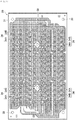
- Fig. 2A is a view of the phosphor substrate 30 of the present embodiment and is a plan view (seen from the front surface 31) in which the phosphor layer 36 omitted.
- Fig. 2B is a plan view (seen from the front surface 31) of the phosphor substrate 30 of the present embodiment.
- the bottom view of the phosphor substrate 30 of the present embodiment is the same as the view of the light emitting substrate 10 seen from the rear surface 33.
- the partial cross-sectional view of the phosphor substrate 30 of the present embodiment is the same as the view when the light emitting element 20 is removed from the partial cross-sectional view of Fig. 1C . That is, the phosphor substrate 30 of the present embodiment is rectangular as an example, when seen from the front surface 31 and the rear surface 33.
- the phosphor substrate 30 of the present embodiment includes an insulating layer 32 (an example of an insulating substrate), an electrode layer 34, a phosphor layer 36, and a rear surface pattern layer 38 (see Figs. 1B , 1C , and 2A , and 2B ).
- the phosphor layer 36 is not shown in Fig. 2A , the phosphor layer 36 is, for example, disposed on a portion of the front surface 31 of the insulating layer 32 and the electrode layer 34, other than a plurality of electrode pairs 34A which will be described later, as shown in Fig. 2B .
- the phosphor substrate 30 is formed with six through holes 39 at four portions near the four corners and two portions near the center.
- the six through holes 39 are used as positioning holes during the manufacturing of the phosphor substrate 30 and the light emitting substrate 10.
- the six through holes 39 are used as mounting screw holes for ensuring a heat-drawing effect (preventing warping and floating of the substrate) of a (light emitting) lamp housing.
- the phosphor substrate 30 of the present embodiment is manufactured by processing (etching or the like) a double-sided plate (hereinafter, referred to as a motherboard MB. see Fig. 3A ) in which copper foil layers are provided on both sides of an insulating plate, and CS-3305A manufactured by Risho Kogyo Co., Ltd. is used as an example of the motherboard MB.
- a shape thereof is, for example, rectangular when seen from the front surface 31 and the rear surface 33.
- a material thereof is, for example, an insulating material containing a bismaleimide resin and a glass cloth.
- a thickness thereof is, for example, 100 ⁇ m to 200 ⁇ m.
- Coefficients of thermal expansion (CTE) thereof in a vertical direction and a horizontal direction are, for example, equal to or less than 10 ppm/°C in a range of 50°C to 100°C, respectively. From another point of view, each of the coefficients of thermal expansion (CTE) in the vertical direction and the horizontal direction is, for example, 6 ppm/K. This value is substantially the same as that of the light emitting element 20 of the present embodiment (90% to 110%, that is, within ⁇ 10%).
- a glass transition temperature thereof is, for example, higher than 300°C.
- a storage elastic modulus is, for example, greater than 1.0 ⁇ 10 10 Pa and smaller than 1.0 ⁇ 10 11 Pa in a range of 100°C to 300°C.
- the electrode layer 34 of the present embodiment is a metal layer provided on the front surface 31 side of the insulating layer 32.
- the electrode layer 34 of this embodiment is, for example, a copper foil layer (a layer formed of Cu).
- the electrode layer 34 of the present embodiment is formed so that at least the surface thereof contains copper.
- the electrode layer 34 has a pattern provided on the insulating layer 32, and is electrically connected to a terminal (not shown) to which a connector (not shown) is bonded.
- the electrode layer 34 supplies electric power supplied from an external power source (not shown) through the connector to the plurality of light emitting elements 20 at the time of configuring the light emitting substrate 10. Accordingly, a part of the electrode layer 34 is the plurality of electrode pairs 34A to which the plurality of light emitting elements 20 are bonded.
- the plurality of electrode pairs 34A are also arranged over the entire front surface 31 (see Fig. 2A ).
- a portion of the electrode layer 34 other than the plurality of electrode pairs 34A is referred to as a wiring portion 34B.
- the plurality of electrode pairs 34A protrude outward from the wiring portion 34B in a thickness direction of the insulating layer 32 (phosphor substrate 30).
- a region of the front surface 31 of the insulating layer 32 where the electrode layer 34 is disposed is, for example, a region (area) that is equal to or more than 60% of the front surface 31 of the insulating layer 32 (see Fig. 2A ).
- the phosphor layer 36 of the present embodiment is, for example, disposed on a portion of the front surface 31 of the insulating layer 32 and the electrode layer 34, other than the plurality of electrode pairs 34A. That is, the phosphor layer 36 is disposed in a region of the electrode layer 34 other than the plurality of electrode pairs 34A.
- the region of the front surface 31 of the insulating layer 32 where the phosphor layer 36 is disposed is, for example, a region that is equal to or more than 80% of the front surface 31 of the insulating layer 32.
- the phosphor layer 36 of the present embodiment is, for example, an insulating layer containing a phosphor and a binder, which will be described later.
- the phosphor contained in the phosphor layer 36 is fine particles held in a state of being dispersed in a binder, and has a property of exciting the light emitted from the LED 22 of each light emitting element 20 as excitation light.
- the phosphor of the present embodiment has a property that the light emission peak wavelength when the light emitted by the light emitting element 20 is used as excitation light is in a visible light region.
- the binder may be, for example, an epoxy-based binder, an acrylate-based binder, or a silicone-based binder, and may have an insulating property equivalent to that of the binder contained in a solder resist.
- the phosphor contained in the phosphor layer 36 of the present embodiment is, for example, at least one or more phosphors selected from the group consisting of an ⁇ -type sialon phosphor containing Eu, a ⁇ -type sialon phosphor containing Eu, a CASN phosphor containing Eu, and a SCASN phosphor containing Eu.
- the phosphor described above is an example of the present embodiment, and may be a phosphor other than the phosphor described above, such as YAG, LuAG, BOS, and other visible light-excited phosphors.
- the ⁇ -type sialon phosphor containing Eu is represented by general formula: M x Eu y Si 12 - (m + n) Al (m + n) O n N 16-n .
- examples of a nitride phosphor include a CASN phosphor containing Eu, a SCASN phosphor containing Eu, and the like.
- the CASN phosphor containing Eu is, for example, a red phosphor which is represented by the formula CaAlSiN 3 :Eu 2+ in which Eu 2+ is used as an activator and a crystal formed of alkaline earth silicate is used as a base.
- the SCASN phosphor containing Eu is excluded.
- the SCASN phosphor containing Eu is, for example, a red phosphor which is represented by the formula (Sr,Ca)AlSiN 3 :Eu 2+ in which Eu 2+ is used as an activator and a crystal formed of alkaline earth silicate is used as a base.
- the rear surface pattern layer 38 of the present embodiment is a metal layer provided on the rear surface 33 side of the insulating layer 32.
- the rear surface pattern layer 38 of this embodiment is, for example, a copper foil layer (a layer formed of Cu).
- the rear surface pattern layer 38 is a layer in which a plurality of rectangular blocks arranged linearly along a longitudinal direction of the insulating layer 32 are arranged to be adjacent to each other by shifting phase in a short direction.
- the rear surface pattern layer 38 is, for example, an independent floating layer. In addition, the rear surface pattern layer 38 overlaps with the region that is equal to or more than 80% of the electrode layer 34 disposed on the front surface 31, for example, in a thickness direction of the insulating layer 32 (phosphor substrate 30).
- the method for manufacturing the light emitting substrate 10 of the present embodiment includes a first step, a second step, a third step, a fourth step, and a fifth step, and each step is performed in this order.
- Fig. 3A is a diagram showing a start time and an end time of the first step.
- the first step is a step of forming a pattern 34C that is the same as the electrode layer 34, when seen from the thickness direction, on the front surface 31 of the motherboard MB, and the rear surface pattern layer 38 on the rear surface 33. This step is performed, for example, by etching using a mask pattern (not shown).
- Fig. 3B is a diagram showing a start time and an end time of the second step.
- the second step is a step of half-etching (etching halfway in the thickness direction) of a part of the pattern 34C. In a case where this step ends, as a result, the electrode layer 34 including the plurality of electrode pairs 34A and the wiring portion 34B is formed. This step is performed, for example, by etching using a mask pattern (not shown).
- Fig. 3C is a diagram showing a start time and an end time of the third step.
- the third step is a step of applying a phosphor coating material 36C to the entire surface of the front surface 31 of the insulating layer 32, that is, the surface on which the electrode layer 34 is formed.
- the phosphor coating material 36C is applied by printing.
- the phosphor coating material 36C is applied thicker than all of the electrode pairs 34A.
- Fig. 3D is a diagram showing a start time and an end time of the fourth step.
- the fourth step is a step of removing a part of the phosphor layer 36 obtained by curing the phosphor coating material 36C and exposing an upper surface of all of the electrode pairs 34A.
- the binder of the phosphor coating material 36C is, for example, a thermosetting resin
- the phosphor coating material 36C is cured by heating and then the surface of the phosphor layer 36 is polished.
- the binder of the phosphor coating material 36C is, for example, a UV curable resin (photosensitive resin)
- a mask pattern is applied to a portion (coating material opening) overlapping each bonded surface 34A1 to expose UV light, the portion other than the mask pattern is UV-cured, and a non-exposed portion (uncured portion) is removed with a resin removing liquid to expose each bonded surface 34A1.
- after-curing is performed by applying heat (photo development method) .
- the phosphor substrate 30 of the present embodiment is manufactured.
- Fig. 3E is a diagram showing a start time and an end time of the fifth step.
- the fifth step is a step of mounting a plurality of light emitting elements 20 on the phosphor substrate 30.
- a solder paste SP is printed on each upper surface of the plurality of electrode pairs 34A of the phosphor substrate 30, and the solder paste SP is melted in a state where each electrode of the plurality of light emitting elements 20 is positioned on each upper surface of the plurality of electrode pairs 34A.
- each light emitting element 20 is bonded to each electrode pair 34A. That is, this step is performed by, for example, a reflow step.
- Fig. 4 is a diagram for explaining the light emitting operation of the light emitting substrate 10 of the present embodiment.
- the power supply is started from the external power source (not shown) to the electrode layer 34 through the connector (not shown), the plurality of light emitting elements 20 emit light L radially, and some light L reaches the front surface 31 of the phosphor substrate 30.
- the behavior of the light L will be described separately according to a traveling direction of the emitted light L.
- Some light L emitted from each light emitting element 20 is emitted to the outside without being incident to the phosphor layer 36.
- a wavelength of the light L remains as the same as the wavelength of the light L, in a case of being emitted from each light emitting element 20.
- the light of the LED 22 itself in some light L emitted from each light emitting element 20 is incident to the phosphor layer 36.
- the "light of the LED 22 itself in some light L” described above is light of the emitted light L that is not color-converted by the phosphor (phosphor sealing layer 24) of each light emitting element 20 (CSP itself), that is, light of the LED 22 itself (for example, blue (wavelength is approximately 470 nm) color).
- the phosphor excites and emits excitation light.
- the reason why the phosphor is excited is that the phosphor dispersed in the phosphor layer 36 uses a phosphor (visible light excited phosphor) having an excitation peak in blue light. Along with this, a part of the energy of the light L is used for exciting the phosphor, so that the light L loses a part of the energy. As a result, the wavelength of the light L is converted (wavelength conversion is performed) . For example, depending on the type of phosphor in the phosphor layer 36 (for example, in a case where a red CASN is used as the phosphor), the wavelength of light L becomes longer (for example, 650 nm or the like).
- the excitation light in the phosphor layer 36 may be emitted from the phosphor layer 36 as it is, but some of the excitation light goes to the lower electrode layer 34. Then, some of the excitation light is emitted to the outside by reflection on the electrode layer 34.
- the wavelength of the excitation light by the phosphor of the phosphor layer 36 is equal to or more than 600 nm, the reflection effect can be expected, even if the electrode layer 34 is formed of Cu.
- the wavelength of the light L differs from the above example depending on the type of the phosphor in the phosphor layer 36, but in any case, the wavelength conversion of the light L is performed.
- a reflection effect can be expected, if the electrode layer 34 or its surface is formed of, for example, Ag (plating) .
- a white reflective layer may be provided on the lower side (insulating layer 32 side) of the phosphor layer 36.
- the reflective layer is provided with, for example, a white coating material such as a titanium oxide filler.
- the light L emitted by each light emitting element 20 (the light L emitted radially by each light emitting element 20) is irradiated to the outside together with the excitation light through a plurality of optical paths as described above. Therefore, in a case where a light emission wavelength of the phosphor contained in the phosphor layer 36 and a light emission wavelength of the phosphor (phosphor sealing layer 24) that seals (or covers) the LED 22 of the light emitting element 20 (CSP) are different from each other, the light emitting substrate 10 of the present embodiment emits a bundle of the light L, in a case of being emitted by each light emitting element 20, by setting it as a bundle of the light L containing the light L at a wavelength different from the wavelength of the light L, in a case of being emitted by each light emitting element 20, together with the excitation light.
- the light emitting substrate 10 of the present embodiment emits a bundle of the light L, in a case of being emitted by each light emitting element 20, by setting it as a bundle of the light L containing the light L at a wavelength longer than the wavelength of the light L, in a case of being emitted by each light emitting element 20, together with the excitation light.
- the light emitting substrate 10 of the present embodiment emits a bundle of the light L, in a case of being emitted by each light emitting element 20, by setting it as a bundle of the light L containing the light L at a wavelength same as the wavelength of the light L, in a case of being emitted by each light emitting element 20, together with the excitation light.
- Fig. 5 is a diagram for explaining a light emitting operation of a light emitting substrate 10A of a comparative embodiment.
- the light emitting substrate 10A of the comparative embodiment (a substrate 30A on which the plurality of light emitting elements 20 are mounted) has the same configuration as the light emitting substrate 10 (phosphor substrate 30) of the present embodiment except that the phosphor layer 36 is not provided.
- the light L emitted from each light emitting element 20 and incident to the front surface 31 of the substrate 30A is reflected or scattered without converting the wavelength. Accordingly, in the case of the substrate 30A of the comparative embodiment, it is not possible to adjust the light to light having light emission color different from the light emitted by the light emitting element 20, in a case where the light emitting element 20 is mounted. That is, in a case of the light emitting substrate 10A of the comparative embodiment, it is not possible to adjust the light to light having light emission color different from the light emitted by the light emitting element 20.
- the phosphor layer 36 is provided on the front surface 31 of the insulating layer 32. Accordingly, some of the light L emitted from each light emitting element 20 is incident to the phosphor layer 36, wavelength-converted by the phosphor layer 36, and irradiated to the outside. In this case, some of the light L radially emitted from each light emitting element 20 is incident to the phosphor layer 36 to excite the phosphor contained in the phosphor layer 36 and generate the excitation light.
- Fig. 6 is a graph showing a result of a first test of the correlated color temperature of the light emitting substrate 10 of the present embodiment.
- Fig. 7 is a graph showing a result of the second test of the correlated color temperature of the light emitting substrate 10 of the present embodiment.
- the first test is a test to obtain a result by investigating a relationship between a current (mA) and a correlated color temperature (K) of the plurality of light emitting elements 20, in a case where the power is supplied to the light emitting substrate 10 including the plurality of light emitting elements 20 having the correlated color temperature approximately at 2200 K to 2300 K to generate light.
- HE (1) and HE (2) indicate a case where the structure of the electrode layer 34 is the same as that of the present embodiment
- FLT (1) and FLT (2) indicate a case where thicknesses of the pair of electrode pair 34A and the wiring portion 34B of the electrode layer 34 are the same (modification example) .
- the correlated color temperature of the light L emitted by the light emitting substrate 10 is lower than the correlated color temperature of the plurality of light emitting elements 20. That is, in the case of the present embodiment (including the modification example described above), the correlated color temperature could be shifted by providing the phosphor layer 36.
- the second test is a test to obtain a result by investigating a relationship between a current (mA) and a correlated color temperature (K) of the plurality of light emitting elements 20, in a case where the power is supplied to the light emitting substrate 10 including the plurality of light emitting elements 20 having the correlated color temperature approximately at 2900 K to 3000 K to generate light.
- HE (1) indicates a case where the structure of the electrode layer 34 is the same structure as that of the present embodiment
- FLT (1) and FLT (2) indicate a case where thicknesses of the pair of electrode pair 34A and the wiring portion 34B of the electrode layer 34 are the same (modification example) .
- the correlated color temperature of the light L emitted by the light emitting substrate 10 is lower than the correlated color temperature of the plurality of light emitting elements 20. That is, in the case of the present embodiment (including the modification example described above), the correlated color temperature could be shifted by providing the phosphor layer 36.
- the phosphor substrate 30 of the present embodiment in a case where the light emitting element 20 is mounted, it is possible to adjust the light L emitted from the phosphor substrate 30 to light having a light emission color different from the light L emitted by the light emitting element 20.
- the light emitting substrate 10 of the present embodiment it is possible to adjust the light L emitted from the phosphor substrate 30 to the light L having a light emission color different from the light L emitted by the light emitting element 20.
- the light emitting substrate 10 of the present embodiment it is possible to irradiate the outside with light L having a light emission color different from the light L emitted by the light emitting element 20.
- the light emitting substrate 10 of the present embodiment emits a bundle of the light L, in a case of being emitted by each light emitting element 20, by setting it as a bundle of the light L containing the light L at a wavelength same as the wavelength of the light L, in a case of being emitted by each light emitting element 20, together with the excitation light.
- spots are generated in the light L irradiated to the outside due to an arrangement interval of each light emitting element 20.
- the larger the spot of light L the larger the glare.
- the phosphor layer 36 is provided between the adjacent light emitting elements 20. Accordingly, the excitation light is also emitted from the phosphor layer 36.
- this effect is effective, in a case where the phosphor layer 36 is provided over the entire surface of the insulating layer 32, specifically, in a case where a region of the front surface 31 of the insulating layer 32 where the phosphor layer 36 is disposed is a region that is 80% or more of the front surface 31.
- the phosphor layer 36 is provided between the adjacent light emitting elements 20 (see Fig. 2B ) .
- the binder of the phosphor layer 36 has an insulating property equivalent to that of the binder contained in, for example, a solder resist. That is, in a case of the present embodiment, the phosphor layer 36 functions as a solder resist.
- the phosphor contained in the phosphor layer 36 is a CASN phosphor containing Eu, and the phosphor layer 36 is provided on the wiring portion 34B formed of Cu. Accordingly, for example, in a case where each light emitting element 20 emits white light L, the excitation light from the CASN phosphor contained in the phosphor layer 36 has an improved light emission efficiency due to reflection by Cu constituting a lower layer electrode (in the configuration of the present embodiment, there is a light reflection effect of Cu). Then, in the present embodiment, by the effect, it is possible to adjust the white light L to a warmer color light (color in which the correlated color temperature is shifted to the lower temperature side) (see Figs.
- the plurality of light emitting elements 20 use a heat sink (not shown) and a cooling fan (not shown) during the light emitting operation to dissipate heat (cool) the phosphor substrate 30 to be, for example, room temperature to 50°C to 100°C. Accordingly, the heat generated in a case of light emission of the LED 22 is diffused to the entire substrate to enhance the heat-drawing effect on the housing.
- a region of the front surface 31 of the insulating layer 32 where the electrode layer 34 is disposed is, for example, a region (area) that is equal to or more than 60% of the front surface 31 of the insulating layer 32 (see Fig. 2A ).
- the electrode layer 34 (wiring portion 34B) of the present embodiment functions as a heat radiating plate for heat generated from the plurality of light emitting elements 20, in addition to the function as an electric path for power supply. Therefore, the light emitting element 20 (LED 22) can stably emit light L in a situation where it is not easily affected by heat.
- an example of the light emitting element 20 is a CSP.
- an example of the light emitting element 20 may be other than the CSP.
- it may simply be equipped with a flip chip.
- it can also be applied to the substrate itself of a COB device.
- the plurality of light emitting elements 20 are mounted on the phosphor substrate 30 and the light emitting substrate 10 includes the plurality of light emitting elements 20 (see Fig. 1A ).
- the number of light emitting elements 20 mounted on the phosphor substrate 30 may be at least one or more.
- the number of light emitting elements 20 mounted on the light emitting substrate 10 may be at least one or more.
- the rear surface pattern layer 38 is provided on the rear surface 33 of the phosphor substrate 30 (see Fig. 1B ).
- the first effect is exhibited even if the rear surface 33 of the phosphor substrate 30 is not provided with the rear surface pattern layer 38. Therefore, even if the embodiment is different from the phosphor substrate 30 and the light emitting substrate 10 of the present embodiment only in that the rear surface 33 is not provided with the rear surface pattern layer 38, it can be said that this embodiment belongs to the technical scope of the present invention.
- the phosphor layer 36 is, for example, disposed on a portion of the front surface 31 of the insulating layer 32 and the electrode layer 34, other than the plurality of electrode pairs 34A (see Fig. 2B ).
- the first effect is exhibited, even if the phosphor layer is not disposed over the entire region of the portion of the front surface 31 of the phosphor substrate 30 other than the plurality of electrode pair 34A.
- CS-3305A manufactured by Risho Kogyo Co., Ltd. is used as the motherboard MB in manufacturing the phosphor substrate 30 and the light emitting substrate 10.
- this is merely an example, and different motherboard MBs may be used.
- the light emitting substrate 10 of the present embodiment (including the modification example thereof) can be applied to a lighting device in combination with other constituent elements.
- Other constituent elements in this case are a power source that supplies electric power for causing the light emitting element 20 of the light emitting substrate 10 to emit light, and the like.
Landscapes
- Engineering & Computer Science (AREA)
- Microelectronics & Electronic Packaging (AREA)
- Power Engineering (AREA)
- Computer Hardware Design (AREA)
- Manufacturing & Machinery (AREA)
- Physics & Mathematics (AREA)
- Spectroscopy & Molecular Physics (AREA)
- Condensed Matter Physics & Semiconductors (AREA)
- General Physics & Mathematics (AREA)
- General Engineering & Computer Science (AREA)
- Led Device Packages (AREA)
- Arrangement Of Elements, Cooling, Sealing, Or The Like Of Lighting Devices (AREA)
- Non-Metallic Protective Coatings For Printed Circuits (AREA)
Abstract
Description
- The present invention relates to a phosphor substrate, a light emitting substrate, and a lighting device.
-
Patent Document 1 discloses an LED lighting equipment including a substrate on which a light emitting element (LED element) is mounted. In this LED lighting equipment, a reflective material is provided on a surface of the substrate to improve light emitting efficiency. - [Patent Document 1]
Chinese Patent Publication No. 106163113 - However, in a case of a configuration disclosed in
Patent Document 1, it is not possible to adjust light emitted by the LED lighting equipment by the reflective material to light having a light emission color different from the light emitted by the light emitting element. - An object of the present invention is to provide a phosphor substrate capable of adjusting light emitted from the phosphor substrate, in a case where a light emitting element is mounted, to light having an emission color different from light emitted by the light emitting element.
- A phosphor substrate according to a first aspect of the present invention is a phosphor substrate having at least one light emitting element mounted on one surface, and includes an insulating substrate, at least one pair of electrode pair which is disposed on one surface of the insulating substrate and bonded to the light emitting element, and a phosphor layer which is disposed on one surface of the insulating substrate and includes a phosphor in which a light emission peak wavelength, in a case where light emitted by the light emitting element is used as excitation light, is in a visible light region.
- A phosphor substrate according to a second aspect of the present invention is a phosphor substrate having a plurality of light emitting elements mounted on one surface, and includes an insulating substrate, a plurality of electrode pairs which are disposed on one surface of the insulating substrate and bonded to the plurality of light emitting elements, and a phosphor layer which is disposed on one surface of the insulating substrate and includes a phosphor in which a light emission peak wavelength, in a case where light emitted by the plurality of light emitting element is used as excitation light, is in a visible light region.
- In the phosphor substrate according to a third aspect of the present invention according to the phosphor substrate according to the second aspect, each of the plurality of electrode pairs is a part of an electrode layer disposed on one surface of the insulating substrate, and a region of the one surface of the insulating substrate, where the electrode layer is disposed is a region which is equal to or more than 60% of the one surface of the insulating substrate.
- In the phosphor substrate according to a fourth aspect of the present invention according to the phosphor substrate according to the third aspect, at least a part of the phosphor layer is disposed in a region other than a region of the one surface of the insulating substrate where the plurality of electrode pairs are disposed.
- In the phosphor substrate according to a fifth aspect of the present invention according to the phosphor substrate according to the third or fourth aspect, at least a part of the phosphor layer is disposed in a region of the electrode layer other than the plurality of electrode pairs.
- In the phosphor substrate according to a sixth aspect of the present invention according to the phosphor substrate according to any one of the second to fifth aspects, a region of the one surface of the insulating substrate, where the phosphor layer is disposed, is a region that is equal to or more than 80% of the one surface of the insulating substrate.
- In the phosphor substrate according to a seventh aspect of the present invention according to the phosphor substrate according to any one of the first to sixth aspects, the phosphor layer is a CASN phosphor containing Eu, and at least a surface of the at least one electrode pair is formed to contain copper.
- In the phosphor substrate according to an eighth aspect of the present invention according to the phosphor substrate according to any one of the first to seventh aspects, the light emitting element is formed as a chip sized package (CSP) in which an LED is incorporated.
- In the phosphor substrate according to a ninth aspect of the present invention according to the phosphor substrate according to the eighth aspect, a correlated color temperature of the phosphor is set to a correlated color temperature which is different from a correlated color temperature of a phosphor contained in the CSP.
- Here, the "correlated color temperature of the phosphor" means a correlated color temperature of the light emission color of the phosphor (hereinafter, the same applies).
- In the phosphor substrate according to a tenth aspect of the present invention according to the phosphor substrate according to the eighth aspect, a correlated color temperature of the phosphor is set to a correlated color temperature which is the same as a correlated color temperature of a phosphor contained in the CSP.
- A light emitting substrate according to the first aspect of the present invention includes the phosphor substrate according to any one aspect of the first to tenth aspects, and at least one light emitting element bonded to the at least one electrode pair.
- In the light emitting substrate according to the second aspect of the present invention according to the light emitting substrates according to the first aspect, the light emitting element is formed as a chip sized package (CSP) in which an LED is incorporated.
- In the light emitting substrate according to a third aspect of the present invention according to the light emitting substrate according to the second aspect, a correlated color temperature of the phosphor is set to a correlated color temperature which is different from a correlated color temperature of a phosphor contained in the CSP.
- In the light emitting substrate of a fourth aspect of the present invention according to the light emitting substrate of the second aspect, a correlated color temperature of the phosphor is set to a correlated color temperature which is the same as a correlated color temperature of a phosphor contained in the CSP.
- A lighting device of the present invention includes the light emitting substrate according to any one of the first to fourth aspects, and a power source which supplies electric power for causing the light emitting element to emit light.
- According to the phosphor substrate according to the first and seventh aspects of the present invention, it is possible to adjust light emitted from the phosphor substrate, in a case where a light emitting element is mounted, to light having an emission color different from light emitted by the light emitting element.
- In addition, in the phosphor substrate according to the second to tenth aspects of the present invention, it is possible to reduce glare while adjusting light emitted from the phosphor substrate, in a case where a light emitting element is mounted, to light having an emission color different from light emitted by the light emitting element. Further, the phosphor substrate according to the tenth aspect of the present invention can also exhibit an effect of alleviating a chromaticity variation of the mounted light emitting element by the phosphor layer.
- In addition, in the light emitting substrate of the present invention, it is possible to adjust light emitted from the phosphor substrate to light having an emission color different from light emitted by the light emitting element.
- The objects described above, other objects, features and advantages will be further clarified by the preferred embodiments which will be described later and the accompanying drawings below.
-
Fig. 1A is a plan view of a light emitting substrate of the present embodiment. -
Fig. 1B is a bottom view of the light emitting substrate of the present embodiment. -
Fig. 1C is a partial cross-sectional view of the light emitting substrate taken along a cutting line 1C-1C ofFig. 1A . -
Fig. 2A is a plan view of a phosphor substrate of the present embodiment (the phosphor layer is not shown). -
Fig. 2B is a plan view of the phosphor substrate of the present embodiment. -
Fig. 3A is an explanatory diagram of a first step in a method for manufacturing the light emitting substrate of the present embodiment. -
Fig. 3B is an explanatory diagram of a second step in the method for manufacturing the light emitting substrate of the present embodiment. -
Fig. 3C is an explanatory diagram of a third step in the method for manufacturing the light emitting substrate of the present embodiment. -
Fig. 3D is an explanatory diagram of a fourth step in the method for manufacturing the light emitting substrate according to the present embodiment. -
Fig. 3E is an explanatory diagram of a fifth step in the method for manufacturing the light emitting substrate according to the present embodiment. -
Fig. 4 is a diagram for explaining a light emitting operation of the light emitting substrate of the present embodiment. -
Fig. 5 is a diagram for explaining a light emitting operation of a light emitting substrate of a comparative embodiment. -
Fig. 6 is a graph showing a result of a first test of a correlated color temperature of the light emitting substrate of the present embodiment. -
Fig. 7 is a graph showing a result of a second test of the correlated color temperature of the light emitting substrate of the present embodiment. - Hereinafter, a configuration and function of a
light emitting substrate 10 of the present embodiment will be described with reference toFigs. 1A to 1C ,2A , and2B . Then, a method for manufacturing thelight emitting substrate 10 of the present embodiment will be described with reference toFigs. 3A to 3E . Next, a light emitting operation of thelight emitting substrate 10 of the present embodiment will be described with reference toFig. 4 . After that, effects of the present embodiment will be described with reference toFigs. 4 to 7 and the like. In all the drawings referred to in the following description, the same reference numerals are used for the same constituent elements and the description thereof will not be repeated. -
Fig. 1A is a plan view of thelight emitting substrate 10 of the present embodiment (view seen from a front surface 31), andFig. 1B is a bottom view of thelight emitting substrate 10 of the present embodiment (view seen from a rear surface 33).Fig. 1C is a partial cross-sectional view of thelight emitting substrate 10 taken along a cutting line 1C-1C ofFig. 1A . - The
light emitting substrate 10 of the present embodiment is rectangular as an example, when seen from thefront surface 31 and therear surface 33. In addition, thelight emitting substrate 10 of the present embodiment includes a plurality oflight emitting elements 20, aphosphor substrate 30, and electronic components (not shown) such as a connector, a driver IC, and the like. That is, in thelight emitting substrate 10 of the present embodiment, the plurality oflight emitting elements 20 and the electronic components are mounted on thephosphor substrate 30. - The
light emitting substrate 10 of the present embodiment has a function of emitting light, in a case where power is supplied from an external power source (not shown) by directly attaching a lead wire or through a connector. Accordingly, thelight emitting substrate 10 of the present embodiment is used as a main optical component in, for example, a lighting device (not shown). - As an example, each of the plurality of
light emitting elements 20 is formed as a Chip Scale Package (CSP) in which a flip chip LED 22 (hereinafter, referred to as an LED 22) is incorporated (seeFig. 1C ). As the CSP, as shown inFig. 1C , it is preferable that the entire circumference (five surfaces) except a bottom surface of theLED 22 is covered with aphosphor sealing layer 24. Thephosphor sealing layer 24 contains a phosphor, and light of theLED 22 is color-converted by the phosphor of thephosphor sealing layer 24 and emitted to the outside. As shown inFig. 1A , the plurality oflight emitting elements 20 are mounted on thephosphor substrate 30 in a state of being regularly arranged on the front surface 31 (an example of one surface) of thephosphor substrate 30 over the entirefront surface 31. A correlated color temperature of the light emitted by each light emittingelement 20 of the present embodiment is set to 3,018K as an example. In addition, the plurality oflight emitting elements 20 use a heat sink (not shown) and a cooling fan (not shown) during the light emitting operation to dissipate heat (cool) thephosphor substrate 30 to be, for example, room temperature to 50°C to 100°C. Here, to supplement the meaning of "to" used in the numerical range in the present specification, for example, "50°C to 100°C" means "equal to or higher than 50°C and equal to or lower than 100°C". In addition, "to" used in the numerical range in this specification means "equal to or more than the description part before "to" and equal to or less than the description part after "to". -
Fig. 2A is a view of thephosphor substrate 30 of the present embodiment and is a plan view (seen from the front surface 31) in which thephosphor layer 36 omitted.Fig. 2B is a plan view (seen from the front surface 31) of thephosphor substrate 30 of the present embodiment. The bottom view of thephosphor substrate 30 of the present embodiment is the same as the view of thelight emitting substrate 10 seen from therear surface 33. In addition, the partial cross-sectional view of thephosphor substrate 30 of the present embodiment is the same as the view when thelight emitting element 20 is removed from the partial cross-sectional view ofFig. 1C . That is, thephosphor substrate 30 of the present embodiment is rectangular as an example, when seen from thefront surface 31 and therear surface 33. - The
phosphor substrate 30 of the present embodiment includes an insulating layer 32 (an example of an insulating substrate), anelectrode layer 34, aphosphor layer 36, and a rear surface pattern layer 38 (seeFigs. 1B ,1C , and2A , and2B ). Although thephosphor layer 36 is not shown inFig. 2A , thephosphor layer 36 is, for example, disposed on a portion of thefront surface 31 of the insulatinglayer 32 and theelectrode layer 34, other than a plurality ofelectrode pairs 34A which will be described later, as shown inFig. 2B . - In addition, as shown in
Figs. 1B and2A , thephosphor substrate 30 is formed with six throughholes 39 at four portions near the four corners and two portions near the center. The six throughholes 39 are used as positioning holes during the manufacturing of thephosphor substrate 30 and thelight emitting substrate 10. In addition, the six throughholes 39 are used as mounting screw holes for ensuring a heat-drawing effect (preventing warping and floating of the substrate) of a (light emitting) lamp housing. As will be described later, thephosphor substrate 30 of the present embodiment is manufactured by processing (etching or the like) a double-sided plate (hereinafter, referred to as a motherboard MB. seeFig. 3A ) in which copper foil layers are provided on both sides of an insulating plate, and CS-3305A manufactured by Risho Kogyo Co., Ltd. is used as an example of the motherboard MB. - Hereinafter, main features of the insulating
layer 32 of the present embodiment will be described. - As described above, a shape thereof is, for example, rectangular when seen from the
front surface 31 and therear surface 33. - A material thereof is, for example, an insulating material containing a bismaleimide resin and a glass cloth.
- A thickness thereof is, for example, 100 µm to 200 µm.
- Coefficients of thermal expansion (CTE) thereof in a vertical direction and a horizontal direction are, for example, equal to or less than 10 ppm/°C in a range of 50°C to 100°C, respectively. From another point of view, each of the coefficients of thermal expansion (CTE) in the vertical direction and the horizontal direction is, for example, 6 ppm/K. This value is substantially the same as that of the
light emitting element 20 of the present embodiment (90% to 110%, that is, within ± 10%). - A glass transition temperature thereof is, for example, higher than 300°C.
- A storage elastic modulus is, for example, greater than 1.0 × 10¹⁰ Pa and smaller than 1.0 × 10¹¹ Pa in a range of 100°C to 300°C.
- The
electrode layer 34 of the present embodiment is a metal layer provided on thefront surface 31 side of the insulatinglayer 32. Theelectrode layer 34 of this embodiment is, for example, a copper foil layer (a layer formed of Cu). In other words, theelectrode layer 34 of the present embodiment is formed so that at least the surface thereof contains copper. - The
electrode layer 34 has a pattern provided on the insulatinglayer 32, and is electrically connected to a terminal (not shown) to which a connector (not shown) is bonded. Theelectrode layer 34 supplies electric power supplied from an external power source (not shown) through the connector to the plurality oflight emitting elements 20 at the time of configuring thelight emitting substrate 10. Accordingly, a part of theelectrode layer 34 is the plurality of electrode pairs 34A to which the plurality oflight emitting elements 20 are bonded. In addition, as described above, since the plurality oflight emitting elements 20 of thelight emitting substrate 10 of the present embodiment are regularly arranged over the entirefront surface 31, the plurality of electrode pairs 34A are also arranged over the entire front surface 31 (seeFig. 2A ). A portion of theelectrode layer 34 other than the plurality ofelectrode pairs 34A is referred to as awiring portion 34B. In the present embodiment, as shown inFig. 1C , as an example, the plurality ofelectrode pairs 34A protrude outward from thewiring portion 34B in a thickness direction of the insulating layer 32 (phosphor substrate 30). - A region of the
front surface 31 of the insulatinglayer 32 where theelectrode layer 34 is disposed (occupied area of the electrode layer 34) is, for example, a region (area) that is equal to or more than 60% of thefront surface 31 of the insulating layer 32 (seeFig. 2A ). - As shown in
Fig. 2B , thephosphor layer 36 of the present embodiment is, for example, disposed on a portion of thefront surface 31 of the insulatinglayer 32 and theelectrode layer 34, other than the plurality of electrode pairs 34A. That is, thephosphor layer 36 is disposed in a region of theelectrode layer 34 other than the plurality of electrode pairs 34A. In the present embodiment, the region of thefront surface 31 of the insulatinglayer 32 where thephosphor layer 36 is disposed is, for example, a region that is equal to or more than 80% of thefront surface 31 of the insulatinglayer 32. - The
phosphor layer 36 of the present embodiment is, for example, an insulating layer containing a phosphor and a binder, which will be described later. The phosphor contained in thephosphor layer 36 is fine particles held in a state of being dispersed in a binder, and has a property of exciting the light emitted from theLED 22 of each light emittingelement 20 as excitation light. Specifically, the phosphor of the present embodiment has a property that the light emission peak wavelength when the light emitted by thelight emitting element 20 is used as excitation light is in a visible light region. The binder may be, for example, an epoxy-based binder, an acrylate-based binder, or a silicone-based binder, and may have an insulating property equivalent to that of the binder contained in a solder resist. - Here, the phosphor contained in the
phosphor layer 36 of the present embodiment is, for example, at least one or more phosphors selected from the group consisting of an α-type sialon phosphor containing Eu, a β-type sialon phosphor containing Eu, a CASN phosphor containing Eu, and a SCASN phosphor containing Eu. The phosphor described above is an example of the present embodiment, and may be a phosphor other than the phosphor described above, such as YAG, LuAG, BOS, and other visible light-excited phosphors. - The α-type sialon phosphor containing Eu is represented by general formula: MxEuySi12 - (m + n)Al(m + n)OnN16-n. In the above general formula, M is at least one or more elements containing at least Ca selected from the group consisting of Li, Mg, Ca, Y, and lanthanide elements (here, excluding La and Ce), and in a case where a valence of M is a, ax + 2y = m, x satisfies 0 < x ≦ 1.5, 0.3 ≦ m < 4.5, and 0 < n < 2.25.
- The β-type sialon phosphor containing Eu is a phosphor in which divalent europium (Eu2+) is dissolved as a light emitting center in β-type sialon represented by general formula: Si6-zAlzOzN8-z (z = 0.005 to 1) .
- In addition, examples of a nitride phosphor include a CASN phosphor containing Eu, a SCASN phosphor containing Eu, and the like.
- The CASN phosphor containing Eu (an example of a nitride phosphor) is, for example, a red phosphor which is represented by the formula CaAlSiN3:Eu2+ in which Eu2+ is used as an activator and a crystal formed of alkaline earth silicate is used as a base. In the definition of the CASN phosphor containing Eu in the present specification, the SCASN phosphor containing Eu is excluded.
- The SCASN phosphor containing Eu (an example of a nitride phosphor) is, for example, a red phosphor which is represented by the formula (Sr,Ca)AlSiN3:Eu2+ in which Eu2+ is used as an activator and a crystal formed of alkaline earth silicate is used as a base.
- The rear
surface pattern layer 38 of the present embodiment is a metal layer provided on therear surface 33 side of the insulatinglayer 32. The rearsurface pattern layer 38 of this embodiment is, for example, a copper foil layer (a layer formed of Cu). - As shown in
Fig. 1B , the rearsurface pattern layer 38 is a layer in which a plurality of rectangular blocks arranged linearly along a longitudinal direction of the insulatinglayer 32 are arranged to be adjacent to each other by shifting phase in a short direction. - The rear
surface pattern layer 38 is, for example, an independent floating layer. In addition, the rearsurface pattern layer 38 overlaps with the region that is equal to or more than 80% of theelectrode layer 34 disposed on thefront surface 31, for example, in a thickness direction of the insulating layer 32 (phosphor substrate 30). - The above is the description of the configuration of the
light emitting substrate 10 and thephosphor substrate 30 of the present embodiment. - Next, a method for manufacturing the
light emitting substrate 10 of the present embodiment will be described with reference toFigs. 3A to 3E . The method for manufacturing thelight emitting substrate 10 of the present embodiment includes a first step, a second step, a third step, a fourth step, and a fifth step, and each step is performed in this order. -
Fig. 3A is a diagram showing a start time and an end time of the first step. The first step is a step of forming apattern 34C that is the same as theelectrode layer 34, when seen from the thickness direction, on thefront surface 31 of the motherboard MB, and the rearsurface pattern layer 38 on therear surface 33. This step is performed, for example, by etching using a mask pattern (not shown). -
Fig. 3B is a diagram showing a start time and an end time of the second step. The second step is a step of half-etching (etching halfway in the thickness direction) of a part of thepattern 34C. In a case where this step ends, as a result, theelectrode layer 34 including the plurality ofelectrode pairs 34A and thewiring portion 34B is formed. This step is performed, for example, by etching using a mask pattern (not shown). -
Fig. 3C is a diagram showing a start time and an end time of the third step. The third step is a step of applying aphosphor coating material 36C to the entire surface of thefront surface 31 of the insulatinglayer 32, that is, the surface on which theelectrode layer 34 is formed. In this step, for example, thephosphor coating material 36C is applied by printing. In this case, thephosphor coating material 36C is applied thicker than all of the electrode pairs 34A. -
Fig. 3D is a diagram showing a start time and an end time of the fourth step. The fourth step is a step of removing a part of thephosphor layer 36 obtained by curing thephosphor coating material 36C and exposing an upper surface of all of the electrode pairs 34A. In a case where the binder of thephosphor coating material 36C is, for example, a thermosetting resin, thephosphor coating material 36C is cured by heating and then the surface of thephosphor layer 36 is polished. In a case where the binder of thephosphor coating material 36C is, for example, a UV curable resin (photosensitive resin), a mask pattern is applied to a portion (coating material opening) overlapping each bonded surface 34A1 to expose UV light, the portion other than the mask pattern is UV-cured, and a non-exposed portion (uncured portion) is removed with a resin removing liquid to expose each bonded surface 34A1. After that, in general, after-curing is performed by applying heat (photo development method) . As a result of the above, thephosphor substrate 30 of the present embodiment is manufactured. -
Fig. 3E is a diagram showing a start time and an end time of the fifth step. The fifth step is a step of mounting a plurality oflight emitting elements 20 on thephosphor substrate 30. In this step, a solder paste SP is printed on each upper surface of the plurality ofelectrode pairs 34A of thephosphor substrate 30, and the solder paste SP is melted in a state where each electrode of the plurality oflight emitting elements 20 is positioned on each upper surface of the plurality of electrode pairs 34A. After that, in a case where the solder paste SP is cooled and solidified, eachlight emitting element 20 is bonded to eachelectrode pair 34A. That is, this step is performed by, for example, a reflow step. - The above is the description of the method for manufacturing the
light emitting substrate 10 of the present embodiment. - Next, the light emitting operation of the
light emitting substrate 10 of the present embodiment will be described with reference toFig. 4. Fig. 4 is a diagram for explaining the light emitting operation of thelight emitting substrate 10 of the present embodiment. - First, in a case where an operation switch (not shown) for operating the plurality of
light emitting elements 20 is turned on, the power supply is started from the external power source (not shown) to theelectrode layer 34 through the connector (not shown), the plurality oflight emitting elements 20 emit light L radially, and some light L reaches thefront surface 31 of thephosphor substrate 30. Hereinafter, the behavior of the light L will be described separately according to a traveling direction of the emitted light L. - Some light L emitted from each light emitting
element 20 is emitted to the outside without being incident to thephosphor layer 36. In this case, a wavelength of the light L remains as the same as the wavelength of the light L, in a case of being emitted from each light emittingelement 20. - In addition, the light of the
LED 22 itself in some light L emitted from each light emittingelement 20 is incident to thephosphor layer 36. Here, the "light of theLED 22 itself in some light L" described above is light of the emitted light L that is not color-converted by the phosphor (phosphor sealing layer 24) of each light emitting element 20 (CSP itself), that is, light of theLED 22 itself (for example, blue (wavelength is approximately 470 nm) color). Then, in a case where the light L of theLED 22 itself collides with the phosphor dispersed in thephosphor layer 36, the phosphor excites and emits excitation light. Here, the reason why the phosphor is excited is that the phosphor dispersed in thephosphor layer 36 uses a phosphor (visible light excited phosphor) having an excitation peak in blue light. Along with this, a part of the energy of the light L is used for exciting the phosphor, so that the light L loses a part of the energy. As a result, the wavelength of the light L is converted (wavelength conversion is performed) . For example, depending on the type of phosphor in the phosphor layer 36 (for example, in a case where a red CASN is used as the phosphor), the wavelength of light L becomes longer (for example, 650 nm or the like). In addition, the excitation light in thephosphor layer 36 may be emitted from thephosphor layer 36 as it is, but some of the excitation light goes to thelower electrode layer 34. Then, some of the excitation light is emitted to the outside by reflection on theelectrode layer 34. As described above, in a case where the wavelength of the excitation light by the phosphor of thephosphor layer 36 is equal to or more than 600 nm, the reflection effect can be expected, even if theelectrode layer 34 is formed of Cu. The wavelength of the light L differs from the above example depending on the type of the phosphor in thephosphor layer 36, but in any case, the wavelength conversion of the light L is performed. For example, in a case where the wavelength of the excitation light is less than 600 nm, a reflection effect can be expected, if theelectrode layer 34 or its surface is formed of, for example, Ag (plating) . In addition, a white reflective layer may be provided on the lower side (insulatinglayer 32 side) of thephosphor layer 36. The reflective layer is provided with, for example, a white coating material such as a titanium oxide filler. - As described above, the light L emitted by each light emitting element 20 (the light L emitted radially by each light emitting element 20) is irradiated to the outside together with the excitation light through a plurality of optical paths as described above. Therefore, in a case where a light emission wavelength of the phosphor contained in the
phosphor layer 36 and a light emission wavelength of the phosphor (phosphor sealing layer 24) that seals (or covers) theLED 22 of the light emitting element 20 (CSP) are different from each other, thelight emitting substrate 10 of the present embodiment emits a bundle of the light L, in a case of being emitted by each light emittingelement 20, by setting it as a bundle of the light L containing the light L at a wavelength different from the wavelength of the light L, in a case of being emitted by each light emittingelement 20, together with the excitation light. For example, thelight emitting substrate 10 of the present embodiment emits a bundle of the light L, in a case of being emitted by each light emittingelement 20, by setting it as a bundle of the light L containing the light L at a wavelength longer than the wavelength of the light L, in a case of being emitted by each light emittingelement 20, together with the excitation light. - Meanwhile, in a case where a light emission wavelength of the phosphor contained in the
phosphor layer 36 and a light emission wavelength of the phosphor (phosphor sealing layer 24) that seals (or covers) theLED 22 of the light emitting element 20 (CSP) are the same as each other (in a case of the same correlated color temperature), thelight emitting substrate 10 of the present embodiment emits a bundle of the light L, in a case of being emitted by each light emittingelement 20, by setting it as a bundle of the light L containing the light L at a wavelength same as the wavelength of the light L, in a case of being emitted by each light emittingelement 20, together with the excitation light. - The above is the description of the light emitting operation of the
light emitting substrate 10 of the present embodiment. - Next, the effect of the present embodiment will be described with reference to the drawings.
- The first effect will be described by comparing the present embodiment with a comparative embodiment (see
Fig. 5 ) described below. Here, in the description of the comparative embodiment, in a case of using the same constituent elements and the like as in the present embodiment, the same names, symbols, and the like as in the case of the present embodiment are used for the constituent elements and the like.Fig. 5 is a diagram for explaining a light emitting operation of alight emitting substrate 10A of a comparative embodiment. Thelight emitting substrate 10A of the comparative embodiment (asubstrate 30A on which the plurality oflight emitting elements 20 are mounted) has the same configuration as the light emitting substrate 10 (phosphor substrate 30) of the present embodiment except that thephosphor layer 36 is not provided. - In the case of the
light emitting substrate 10A of the comparative embodiment, the light L emitted from each light emittingelement 20 and incident to thefront surface 31 of thesubstrate 30A is reflected or scattered without converting the wavelength. Accordingly, in the case of thesubstrate 30A of the comparative embodiment, it is not possible to adjust the light to light having light emission color different from the light emitted by thelight emitting element 20, in a case where thelight emitting element 20 is mounted. That is, in a case of thelight emitting substrate 10A of the comparative embodiment, it is not possible to adjust the light to light having light emission color different from the light emitted by thelight emitting element 20. - On the other hand, in a case of the present embodiment, the
phosphor layer 36 is provided on thefront surface 31 of the insulatinglayer 32. Accordingly, some of the light L emitted from each light emittingelement 20 is incident to thephosphor layer 36, wavelength-converted by thephosphor layer 36, and irradiated to the outside. In this case, some of the light L radially emitted from each light emittingelement 20 is incident to thephosphor layer 36 to excite the phosphor contained in thephosphor layer 36 and generate the excitation light. - Here,
Fig. 6 is a graph showing a result of a first test of the correlated color temperature of thelight emitting substrate 10 of the present embodiment. In addition,Fig. 7 is a graph showing a result of the second test of the correlated color temperature of thelight emitting substrate 10 of the present embodiment. - The first test is a test to obtain a result by investigating a relationship between a current (mA) and a correlated color temperature (K) of the plurality of
light emitting elements 20, in a case where the power is supplied to thelight emitting substrate 10 including the plurality oflight emitting elements 20 having the correlated color temperature approximately at 2200 K to 2300 K to generate light. Here, HE (1) and HE (2) indicate a case where the structure of theelectrode layer 34 is the same as that of the present embodiment, and FLT (1) and FLT (2) indicate a case where thicknesses of the pair ofelectrode pair 34A and thewiring portion 34B of theelectrode layer 34 are the same (modification example) . As the result ofFig. 6 , in any case, the correlated color temperature of the light L emitted by thelight emitting substrate 10 is lower than the correlated color temperature of the plurality oflight emitting elements 20. That is, in the case of the present embodiment (including the modification example described above), the correlated color temperature could be shifted by providing thephosphor layer 36. - In addition, the second test is a test to obtain a result by investigating a relationship between a current (mA) and a correlated color temperature (K) of the plurality of
light emitting elements 20, in a case where the power is supplied to thelight emitting substrate 10 including the plurality oflight emitting elements 20 having the correlated color temperature approximately at 2900 K to 3000 K to generate light. Here, HE (1) indicates a case where the structure of theelectrode layer 34 is the same structure as that of the present embodiment, and FLT (1) and FLT (2) indicate a case where thicknesses of the pair ofelectrode pair 34A and thewiring portion 34B of theelectrode layer 34 are the same (modification example) . As the result ofFig. 7 , in any case, the correlated color temperature of the light L emitted by thelight emitting substrate 10 is lower than the correlated color temperature of the plurality oflight emitting elements 20. That is, in the case of the present embodiment (including the modification example described above), the correlated color temperature could be shifted by providing thephosphor layer 36. - Therefore, according to the
phosphor substrate 30 of the present embodiment, in a case where thelight emitting element 20 is mounted, it is possible to adjust the light L emitted from thephosphor substrate 30 to light having a light emission color different from the light L emitted by thelight emitting element 20. Along with this, according to thelight emitting substrate 10 of the present embodiment, it is possible to adjust the light L emitted from thephosphor substrate 30 to the light L having a light emission color different from the light L emitted by thelight emitting element 20. From another point of view, according to thelight emitting substrate 10 of the present embodiment, it is possible to irradiate the outside with light L having a light emission color different from the light L emitted by thelight emitting element 20. - Meanwhile, in a case where a light emission wavelength of the phosphor contained in the
phosphor layer 36 and a light emission wavelength of the phosphor (phosphor sealing layer 24) that seals (or covers) theLED 22 of the light emitting element 20 (CSP) are the same as each other (in a case of the same correlated color temperature), thelight emitting substrate 10 of the present embodiment emits a bundle of the light L, in a case of being emitted by each light emittingelement 20, by setting it as a bundle of the light L containing the light L at a wavelength same as the wavelength of the light L, in a case of being emitted by each light emittingelement 20, together with the excitation light. In this case, it is possible to exhibit the effect of alleviating a chromaticity variation of the mountedlight emitting element 20 by thephosphor layer 36. - In the case of the comparative embodiment, as shown in
Fig. 5 , spots are generated in the light L irradiated to the outside due to an arrangement interval of each light emittingelement 20. Here, the larger the spot of light L, the larger the glare. - On the other hand, in a case of the present embodiment, as shown in
Fig. 2B , thephosphor layer 36 is provided between the adjacentlight emitting elements 20. Accordingly, the excitation light is also emitted from thephosphor layer 36. - Therefore, according to the present embodiment, it is possible to reduce the glare, compared to the comparative embodiment.
- In particular, this effect is effective, in a case where the
phosphor layer 36 is provided over the entire surface of the insulatinglayer 32, specifically, in a case where a region of thefront surface 31 of the insulatinglayer 32 where thephosphor layer 36 is disposed is a region that is 80% or more of thefront surface 31. - In addition, in the present embodiment, as described above, the
phosphor layer 36 is provided between the adjacent light emitting elements 20 (seeFig. 2B ) . In addition, the binder of thephosphor layer 36 has an insulating property equivalent to that of the binder contained in, for example, a solder resist. That is, in a case of the present embodiment, thephosphor layer 36 functions as a solder resist. - In addition, in a case of the present embodiment, for example, the phosphor contained in the
phosphor layer 36 is a CASN phosphor containing Eu, and thephosphor layer 36 is provided on thewiring portion 34B formed of Cu. Accordingly, for example, in a case where each light emittingelement 20 emits white light L, the excitation light from the CASN phosphor contained in thephosphor layer 36 has an improved light emission efficiency due to reflection by Cu constituting a lower layer electrode (in the configuration of the present embodiment, there is a light reflection effect of Cu). Then, in the present embodiment, by the effect, it is possible to adjust the white light L to a warmer color light (color in which the correlated color temperature is shifted to the lower temperature side) (seeFigs. 6 and7 ). In this case, it is possible to add warm color light to the white light of thelight emitting element 20, and increase a special color rendering index R9 value. This effect is particularly effective for pseudo-white using YAG-based white light (yellow phosphor). - In addition, as described above, the plurality of
light emitting elements 20 use a heat sink (not shown) and a cooling fan (not shown) during the light emitting operation to dissipate heat (cool) thephosphor substrate 30 to be, for example, room temperature to 50°C to 100°C. Accordingly, the heat generated in a case of light emission of theLED 22 is diffused to the entire substrate to enhance the heat-drawing effect on the housing. In a case of the present embodiment, a region of thefront surface 31 of the insulatinglayer 32 where theelectrode layer 34 is disposed (occupied area of the electrode layer 34) is, for example, a region (area) that is equal to or more than 60% of thefront surface 31 of the insulating layer 32 (seeFig. 2A ). - Accordingly, the electrode layer 34 (
wiring portion 34B) of the present embodiment functions as a heat radiating plate for heat generated from the plurality oflight emitting elements 20, in addition to the function as an electric path for power supply. Therefore, the light emitting element 20 (LED 22) can stably emit light L in a situation where it is not easily affected by heat. - The above is the description of the effect of the present embodiment.
- As described above, the present invention has been described with reference to the embodiments and examples described above, but the present invention is not limited to the embodiments and examples described above. The technical scope of the present invention also includes, for example, the following embodiments (modification example).
- For example, in the description of the present embodiment, an example of the
light emitting element 20 is a CSP. However, an example of thelight emitting element 20 may be other than the CSP. For example, it may simply be equipped with a flip chip. In addition, it can also be applied to the substrate itself of a COB device. - In addition, in the description of the present embodiment, the plurality of
light emitting elements 20 are mounted on thephosphor substrate 30 and thelight emitting substrate 10 includes the plurality of light emitting elements 20 (seeFig. 1A ). However, considering a mechanism for explaining a first effect described above, it is clear that the first effect is exhibited even with onelight emitting element 20. Therefore, the number oflight emitting elements 20 mounted on thephosphor substrate 30 may be at least one or more. In addition, the number oflight emitting elements 20 mounted on thelight emitting substrate 10 may be at least one or more. - In addition, in the description of the present embodiment, the rear
surface pattern layer 38 is provided on therear surface 33 of the phosphor substrate 30 (seeFig. 1B ). However, considering a mechanism for explaining the first effect described above, it is clear that the first effect is exhibited even if therear surface 33 of thephosphor substrate 30 is not provided with the rearsurface pattern layer 38. Therefore, even if the embodiment is different from thephosphor substrate 30 and thelight emitting substrate 10 of the present embodiment only in that therear surface 33 is not provided with the rearsurface pattern layer 38, it can be said that this embodiment belongs to the technical scope of the present invention. - In addition, in the description of the present embodiment, the
phosphor layer 36 is, for example, disposed on a portion of thefront surface 31 of the insulatinglayer 32 and theelectrode layer 34, other than the plurality ofelectrode pairs 34A (seeFig. 2B ). However, considering a mechanism for explaining the first effect described above, it is clear that the first effect is exhibited, even if the phosphor layer is not disposed over the entire region of the portion of thefront surface 31 of thephosphor substrate 30 other than the plurality ofelectrode pair 34A. Therefore, even if the embodiment is different from thephosphor substrate 30 and thelight emitting substrate 10 of the present embodiment only in that thephosphor layer 36 is disposed in a range of thefront surface 31 different from that of the present embodiment, it can be said that this embodiment belongs to the technical scope of the present invention. - In addition, in the description of the present embodiment, it has been described that CS-3305A manufactured by Risho Kogyo Co., Ltd. is used as the motherboard MB in manufacturing the
phosphor substrate 30 and thelight emitting substrate 10. However, this is merely an example, and different motherboard MBs may be used. - The
light emitting substrate 10 of the present embodiment (including the modification example thereof) can be applied to a lighting device in combination with other constituent elements. Other constituent elements in this case are a power source that supplies electric power for causing thelight emitting element 20 of thelight emitting substrate 10 to emit light, and the like. - This application claims priority based on
Japanese Patent Application No. 2018-244542 filed on December 27, 2018
Claims (15)
- A phosphor substrate having at least one light emitting element mounted on one surface, the phosphor substrate comprising:an insulating substrate;at least one electrode pair which is disposed on one surface of the insulating substrate and bonded to the light emitting element; anda phosphor layer which is disposed on one surface of the insulating substrate and includes a phosphor in which a light emission peak wavelength, in a case where light emitted by the light emitting element is used as excitation light, is in a visible light region.
- A phosphor substrate having a plurality of light emitting elements mounted on one surface, the phosphor substrate comprising:an insulating substrate;a plurality of electrode pairs which are disposed on one surface of the insulating substrate and bonded to the plurality of light emitting elements; anda phosphor layer which is disposed on one surface of the insulating substrate and includes a phosphor in which a light emission peak wavelength, in a case where light emitted by the plurality of light emitting elements is used as excitation light, is in a visible light region.
- The phosphor substrate according to claim 2,wherein each of the plurality of electrode pairs is a part of an electrode layer disposed on one surface of the insulating substrate, anda region of the one surface of the insulating substrate, where the electrode layer is disposed is a region which is equal to or more than 60% of the one surface of the insulating substrate.
- The phosphor substrate according to claim 3,
wherein at least a part of the phosphor layer is disposed in a region other than a region of the one surface of the insulating substrate where the plurality of electrode pairs are disposed. - The phosphor substrate according to claim 3 or 4,
wherein at least a part of the phosphor layer is disposed in a region of the electrode layer other than the plurality of electrode pairs. - The phosphor substrate according to any one of claims 2 to 5,
wherein a region of the one surface of the insulating substrate, where the phosphor layer is disposed, is a region that is equal to or more than 80% of the one surface of the insulating substrate. - The phosphor substrate according to any one of claims 1 to 6,wherein the phosphor layer is a CASN phosphor containing Eu, andat least a surface of the at least one electrode pair is formed to contain copper.
- The phosphor substrate according to any one of claims 1 to 7,
wherein the light emitting element is formed as a chip sized package (CSP) in which an LED is incorporated. - The phosphor substrate according to claim 8,
wherein a correlated color temperature of the phosphor is set to a correlated color temperature which is different from a correlated color temperature of a phosphor contained in the CSP. - The phosphor substrate according to claim 8,
wherein a correlated color temperature of the phosphor is set to a correlated color temperature which is the same as a correlated color temperature of a phosphor contained in the CSP. - A light emitting substrate comprising:the phosphor substrate according to any one of claims 1 to 10; andat least one light emitting element bonded to the at least one electrode pair.
- The light emitting substrate according to claim 11,
wherein the light emitting element is formed as a chip sized package (CSP) in which an LED is incorporated. - The light emitting substrate according to claim 12,
wherein a correlated color temperature of the phosphor is set to a correlated color temperature which is different from a correlated color temperature of a phosphor contained in the CSP. - The light emitting substrate according to claim 12,
wherein a correlated color temperature of the phosphor is set to a correlated color temperature which is the same as a correlated color temperature of a phosphor contained in the CSP. - A lighting device comprising:the light emitting substrate according to any one of claims 11 to 14; anda power source which supplies electric power for causing the light emitting element to emit light.
Applications Claiming Priority (2)
| Application Number | Priority Date | Filing Date | Title |
|---|---|---|---|
| JP2018244542 | 2018-12-27 | ||
| PCT/JP2019/049687 WO2020137760A1 (en) | 2018-12-27 | 2019-12-18 | Phosphor substrate, light-emitting substrate, and lighting device |
Publications (3)
| Publication Number | Publication Date |
|---|---|
| EP3905348A1 true EP3905348A1 (en) | 2021-11-03 |
| EP3905348A4 EP3905348A4 (en) | 2022-05-11 |
| EP3905348B1 EP3905348B1 (en) | 2024-01-24 |
Family
ID=71129754
Family Applications (1)
| Application Number | Title | Priority Date | Filing Date |
|---|---|---|---|
| EP19905139.2A Active EP3905348B1 (en) | 2018-12-27 | 2019-12-18 | Light-emitting substrate, and lighting device |
Country Status (7)
| Country | Link |
|---|---|
| US (1) | US20220059730A1 (en) |
| EP (1) | EP3905348B1 (en) |
| JP (1) | JPWO2020137760A1 (en) |
| KR (1) | KR20210105891A (en) |
| CN (1) | CN113228314A (en) |
| TW (1) | TW202039790A (en) |
| WO (1) | WO2020137760A1 (en) |
Families Citing this family (1)
| Publication number | Priority date | Publication date | Assignee | Title |
|---|---|---|---|---|
| WO2020137764A1 (en) | 2018-12-27 | 2020-07-02 | デンカ株式会社 | Fluorescent substrate, display device, and lighting device |
Family Cites Families (22)
| Publication number | Priority date | Publication date | Assignee | Title |
|---|---|---|---|---|
| JP4128564B2 (en) * | 2004-04-27 | 2008-07-30 | 松下電器産業株式会社 | Light emitting device |
| KR101361575B1 (en) * | 2007-09-17 | 2014-02-13 | 삼성전자주식회사 | Light Emitting Diode package and method of manufacturing the same |
| JP2012094578A (en) * | 2010-10-25 | 2012-05-17 | Citizen Holdings Co Ltd | Manufacturing method of semiconductor light emitting device |
| JP2012186274A (en) * | 2011-03-04 | 2012-09-27 | Sharp Corp | Light-emitting device, led chip, led wafer and package substrate |
| JP5703997B2 (en) * | 2011-06-29 | 2015-04-22 | 豊田合成株式会社 | Light emitting device |
| KR20130104975A (en) * | 2012-03-16 | 2013-09-25 | 삼성전자주식회사 | Light emitting device |
| JP5910340B2 (en) * | 2012-06-15 | 2016-04-27 | コニカミノルタ株式会社 | LED device and manufacturing method thereof |
| WO2013185836A1 (en) * | 2012-06-15 | 2013-12-19 | Sferrum Gmbh | Led package and method for producing the same |
| JP2014220431A (en) * | 2013-05-09 | 2014-11-20 | 日東電工株式会社 | Circuit board, optical semiconductor device and method of manufacturing the same |
| US9287472B2 (en) * | 2013-06-27 | 2016-03-15 | Nichia Corporation | Light emitting device and method of manufacturing the same |
| CN104282819B (en) * | 2013-07-08 | 2018-08-28 | 光宝电子(广州)有限公司 | Flip-over type LED encapsulation module and its manufacturing method |
| CN105579763B (en) * | 2013-07-10 | 2018-06-01 | 黄金眼公司 | From cooling light source |
| JP6764340B2 (en) * | 2013-08-01 | 2020-09-30 | シグニファイ ホールディング ビー ヴィSignify Holding B.V. | Luminescent device with adapted output spectrum |
| JP6955704B2 (en) * | 2013-10-23 | 2021-10-27 | 株式会社光波 | Light emitting device |
| CN103904072A (en) * | 2014-03-28 | 2014-07-02 | 中山市鸿宝电业有限公司 | High-power LED chip integrated packaging structure |
| US9660161B2 (en) * | 2014-07-07 | 2017-05-23 | Cree, Inc. | Light emitting diode (LED) components including contact expansion frame |
| CN106163113A (en) | 2015-03-23 | 2016-11-23 | 李玉俊 | LED installs lamp bead circuit board light-reflection layer processing technology |
| TWI644454B (en) * | 2015-08-19 | 2018-12-11 | 佰鴻工業股份有限公司 | Light-emitting diode structure |
| JP6582794B2 (en) * | 2015-09-18 | 2019-10-02 | 大日本印刷株式会社 | LED information display panel with snow melting function and LED information display device |
| US9985182B2 (en) * | 2015-12-25 | 2018-05-29 | Citizen Electronics Co., Ltd. | Light-emitting apparatus and color-matching apparatus |
| TWI583028B (en) * | 2016-02-05 | 2017-05-11 | 行家光電股份有限公司 | Light emitting device with beam shaping structure and manufacturing method of the same |
| CN107091412A (en) * | 2016-09-30 | 2017-08-25 | 深圳市玲涛光电科技有限公司 | Strip source and its manufacture method, backlight module, electronic equipment |
-
2019
- 2019-12-18 KR KR1020217018336A patent/KR20210105891A/en active Search and Examination
- 2019-12-18 WO PCT/JP2019/049687 patent/WO2020137760A1/en unknown
- 2019-12-18 CN CN201980085491.5A patent/CN113228314A/en active Pending
- 2019-12-18 JP JP2020563141A patent/JPWO2020137760A1/en active Pending
- 2019-12-18 EP EP19905139.2A patent/EP3905348B1/en active Active
- 2019-12-18 US US17/415,373 patent/US20220059730A1/en active Pending
- 2019-12-23 TW TW108147166A patent/TW202039790A/en unknown
Also Published As
| Publication number | Publication date |
|---|---|
| KR20210105891A (en) | 2021-08-27 |
| EP3905348A4 (en) | 2022-05-11 |
| EP3905348B1 (en) | 2024-01-24 |
| CN113228314A (en) | 2021-08-06 |
| WO2020137760A1 (en) | 2020-07-02 |
| JPWO2020137760A1 (en) | 2021-11-11 |
| US20220059730A1 (en) | 2022-02-24 |
| TW202039790A (en) | 2020-11-01 |
Similar Documents
| Publication | Publication Date | Title |
|---|---|---|
| EP3905347B1 (en) | Light-emitting substrate, and lighting device | |
| EP3905346B1 (en) | Light-emitting substrate, and lighting device | |
| US20230361254A1 (en) | Phosphor board manufacturing method and light-emitting substrate manufacturing method | |
| EP3905348A1 (en) | Phosphor substrate, light-emitting substrate, and lighting device | |
| EP3905349B1 (en) | Light-emitting substrate, and lighting device | |
| EP3905345B1 (en) | Light-emitting substrate, and lighting device | |
| KR20210131338A (en) | A phosphor substrate, a light emitting substrate, a lighting device, a method for manufacturing a phosphor substrate, and a method for manufacturing a light emitting substrate | |
| US20230335685A1 (en) | Phosphor board, light-emitting substrate, and lighting apparatus | |
| KR20210132047A (en) | Circuit board, mounting board, lighting device, manufacturing method of circuit board, and manufacturing method of mounting board |
Legal Events
| Date | Code | Title | Description |
|---|---|---|---|
| STAA | Information on the status of an ep patent application or granted ep patent |
Free format text: STATUS: THE INTERNATIONAL PUBLICATION HAS BEEN MADE |
|
| PUAI | Public reference made under article 153(3) epc to a published international application that has entered the european phase |
Free format text: ORIGINAL CODE: 0009012 |
|
| STAA | Information on the status of an ep patent application or granted ep patent |
Free format text: STATUS: REQUEST FOR EXAMINATION WAS MADE |
|
| 17P | Request for examination filed |
Effective date: 20210701 |
|
| AK | Designated contracting states |
Kind code of ref document: A1 Designated state(s): AL AT BE BG CH CY CZ DE DK EE ES FI FR GB GR HR HU IE IS IT LI LT LU LV MC MK MT NL NO PL PT RO RS SE SI SK SM TR |
|
| A4 | Supplementary search report drawn up and despatched |
Effective date: 20220118 |
|
| RIC1 | Information provided on ipc code assigned before grant |
Ipc: H01L 25/075 20060101ALI20220112BHEP Ipc: H05K 3/28 20060101ALI20220112BHEP Ipc: H01L 33/62 20100101ALI20220112BHEP Ipc: H01L 33/50 20100101AFI20220112BHEP |
|
| DA4 | Supplementary search report drawn up and despatched (deleted) | ||
| RIC1 | Information provided on ipc code assigned before grant |
Ipc: H01L 25/075 20060101ALI20220203BHEP Ipc: H05K 3/28 20060101ALI20220203BHEP Ipc: H01L 33/62 20100101ALI20220203BHEP Ipc: H01L 33/50 20100101AFI20220203BHEP |
|
| DAV | Request for validation of the european patent (deleted) | ||
| DAX | Request for extension of the european patent (deleted) | ||
| RIC1 | Information provided on ipc code assigned before grant |
Ipc: H01L 25/075 20060101ALI20220305BHEP Ipc: H05K 3/28 20060101ALI20220305BHEP Ipc: H01L 33/62 20100101ALI20220305BHEP Ipc: H01L 33/50 20100101AFI20220305BHEP |
|
| RA4 | Supplementary search report drawn up and despatched (corrected) |
Effective date: 20220310 |
|
| STAA | Information on the status of an ep patent application or granted ep patent |
Free format text: STATUS: EXAMINATION IS IN PROGRESS |
|
| 17Q | First examination report despatched |
Effective date: 20221017 |
|
| GRAP | Despatch of communication of intention to grant a patent |
Free format text: ORIGINAL CODE: EPIDOSNIGR1 |
|
| STAA | Information on the status of an ep patent application or granted ep patent |
Free format text: STATUS: GRANT OF PATENT IS INTENDED |
|
| INTG | Intention to grant announced |
Effective date: 20230904 |
|
| GRAS | Grant fee paid |
Free format text: ORIGINAL CODE: EPIDOSNIGR3 |
|
| GRAA | (expected) grant |
Free format text: ORIGINAL CODE: 0009210 |
|
| STAA | Information on the status of an ep patent application or granted ep patent |
Free format text: STATUS: THE PATENT HAS BEEN GRANTED |
|
| AK | Designated contracting states |
Kind code of ref document: B1 Designated state(s): AL AT BE BG CH CY CZ DE DK EE ES FI FR GB GR HR HU IE IS IT LI LT LU LV MC MK MT NL NO PL PT RO RS SE SI SK SM TR |
|
| REG | Reference to a national code |
Ref country code: GB Ref legal event code: FG4D |
|
| REG | Reference to a national code |
Ref country code: CH Ref legal event code: EP |
|
| REG | Reference to a national code |
Ref country code: IE Ref legal event code: FG4D |
|
| REG | Reference to a national code |
Ref country code: DE Ref legal event code: R096 Ref document number: 602019045839 Country of ref document: DE |
|
| P01 | Opt-out of the competence of the unified patent court (upc) registered |
Effective date: 20240123 |
|
| REG | Reference to a national code |
Ref country code: NL Ref legal event code: FP |