EP3905339A1 - Heterojunction semiconductor device with low on-resistance - Google Patents
Heterojunction semiconductor device with low on-resistance Download PDFInfo
- Publication number
- EP3905339A1 EP3905339A1 EP19904187.2A EP19904187A EP3905339A1 EP 3905339 A1 EP3905339 A1 EP 3905339A1 EP 19904187 A EP19904187 A EP 19904187A EP 3905339 A1 EP3905339 A1 EP 3905339A1
- Authority
- EP
- European Patent Office
- Prior art keywords
- current blocking
- layer
- blocking layer
- semiconductor device
- disposed
- Prior art date
- Legal status (The legal status is an assumption and is not a legal conclusion. Google has not performed a legal analysis and makes no representation as to the accuracy of the status listed.)
- Pending
Links
Images


Classifications
-
- H—ELECTRICITY
- H10—SEMICONDUCTOR DEVICES; ELECTRIC SOLID-STATE DEVICES NOT OTHERWISE PROVIDED FOR
- H10D—INORGANIC ELECTRIC SEMICONDUCTOR DEVICES
- H10D30/00—Field-effect transistors [FET]
- H10D30/40—FETs having zero-dimensional [0D], one-dimensional [1D] or two-dimensional [2D] charge carrier gas channels
- H10D30/47—FETs having zero-dimensional [0D], one-dimensional [1D] or two-dimensional [2D] charge carrier gas channels having two-dimensional [2D] charge carrier gas channels, e.g. nanoribbon FETs or high electron mobility transistors [HEMT]
- H10D30/471—High electron mobility transistors [HEMT] or high hole mobility transistors [HHMT]
- H10D30/477—Vertical HEMTs or vertical HHMTs
-
- H—ELECTRICITY
- H10—SEMICONDUCTOR DEVICES; ELECTRIC SOLID-STATE DEVICES NOT OTHERWISE PROVIDED FOR
- H10D—INORGANIC ELECTRIC SEMICONDUCTOR DEVICES
- H10D30/00—Field-effect transistors [FET]
- H10D30/40—FETs having zero-dimensional [0D], one-dimensional [1D] or two-dimensional [2D] charge carrier gas channels
- H10D30/47—FETs having zero-dimensional [0D], one-dimensional [1D] or two-dimensional [2D] charge carrier gas channels having two-dimensional [2D] charge carrier gas channels, e.g. nanoribbon FETs or high electron mobility transistors [HEMT]
- H10D30/471—High electron mobility transistors [HEMT] or high hole mobility transistors [HHMT]
- H10D30/478—High electron mobility transistors [HEMT] or high hole mobility transistors [HHMT] the 2D charge carrier gas being at least partially not parallel to a main surface of the semiconductor body
-
- H—ELECTRICITY
- H10—SEMICONDUCTOR DEVICES; ELECTRIC SOLID-STATE DEVICES NOT OTHERWISE PROVIDED FOR
- H10D—INORGANIC ELECTRIC SEMICONDUCTOR DEVICES
- H10D62/00—Semiconductor bodies, or regions thereof, of devices having potential barriers
- H10D62/10—Shapes, relative sizes or dispositions of the regions of the semiconductor bodies; Shapes of the semiconductor bodies
- H10D62/102—Constructional design considerations for preventing surface leakage or controlling electric field concentration
- H10D62/103—Constructional design considerations for preventing surface leakage or controlling electric field concentration for increasing or controlling the breakdown voltage of reverse-biased devices
- H10D62/105—Constructional design considerations for preventing surface leakage or controlling electric field concentration for increasing or controlling the breakdown voltage of reverse-biased devices by having particular doping profiles, shapes or arrangements of PN junctions; by having supplementary regions, e.g. junction termination extension [JTE]
- H10D62/106—Constructional design considerations for preventing surface leakage or controlling electric field concentration for increasing or controlling the breakdown voltage of reverse-biased devices by having particular doping profiles, shapes or arrangements of PN junctions; by having supplementary regions, e.g. junction termination extension [JTE] having supplementary regions doped oppositely to or in rectifying contact with regions of the semiconductor bodies, e.g. guard rings with PN or Schottky junctions
- H10D62/107—Buried supplementary regions, e.g. buried guard rings
-
- H—ELECTRICITY
- H10—SEMICONDUCTOR DEVICES; ELECTRIC SOLID-STATE DEVICES NOT OTHERWISE PROVIDED FOR
- H10D—INORGANIC ELECTRIC SEMICONDUCTOR DEVICES
- H10D62/00—Semiconductor bodies, or regions thereof, of devices having potential barriers
- H10D62/10—Shapes, relative sizes or dispositions of the regions of the semiconductor bodies; Shapes of the semiconductor bodies
- H10D62/113—Isolations within a component, i.e. internal isolations
- H10D62/114—PN junction isolations
-
- H—ELECTRICITY
- H10—SEMICONDUCTOR DEVICES; ELECTRIC SOLID-STATE DEVICES NOT OTHERWISE PROVIDED FOR
- H10D—INORGANIC ELECTRIC SEMICONDUCTOR DEVICES
- H10D62/00—Semiconductor bodies, or regions thereof, of devices having potential barriers
- H10D62/10—Shapes, relative sizes or dispositions of the regions of the semiconductor bodies; Shapes of the semiconductor bodies
- H10D62/117—Shapes of semiconductor bodies
-
- H—ELECTRICITY
- H10—SEMICONDUCTOR DEVICES; ELECTRIC SOLID-STATE DEVICES NOT OTHERWISE PROVIDED FOR
- H10D—INORGANIC ELECTRIC SEMICONDUCTOR DEVICES
- H10D62/00—Semiconductor bodies, or regions thereof, of devices having potential barriers
- H10D62/10—Shapes, relative sizes or dispositions of the regions of the semiconductor bodies; Shapes of the semiconductor bodies
- H10D62/124—Shapes, relative sizes or dispositions of the regions of semiconductor bodies or of junctions between the regions
-
- H—ELECTRICITY
- H10—SEMICONDUCTOR DEVICES; ELECTRIC SOLID-STATE DEVICES NOT OTHERWISE PROVIDED FOR
- H10D—INORGANIC ELECTRIC SEMICONDUCTOR DEVICES
- H10D62/00—Semiconductor bodies, or regions thereof, of devices having potential barriers
- H10D62/10—Shapes, relative sizes or dispositions of the regions of the semiconductor bodies; Shapes of the semiconductor bodies
- H10D62/17—Semiconductor regions connected to electrodes not carrying current to be rectified, amplified or switched, e.g. channel regions
- H10D62/213—Channel regions of field-effect devices
- H10D62/221—Channel regions of field-effect devices of FETs
- H10D62/235—Channel regions of field-effect devices of FETs of IGFETs
- H10D62/292—Non-planar channels of IGFETs
-
- H—ELECTRICITY
- H10—SEMICONDUCTOR DEVICES; ELECTRIC SOLID-STATE DEVICES NOT OTHERWISE PROVIDED FOR
- H10D—INORGANIC ELECTRIC SEMICONDUCTOR DEVICES
- H10D62/00—Semiconductor bodies, or regions thereof, of devices having potential barriers
- H10D62/80—Semiconductor bodies, or regions thereof, of devices having potential barriers characterised by the materials
- H10D62/82—Heterojunctions
- H10D62/824—Heterojunctions comprising only Group III-V materials heterojunctions, e.g. GaN/AlGaN heterojunctions
-
- H—ELECTRICITY
- H10—SEMICONDUCTOR DEVICES; ELECTRIC SOLID-STATE DEVICES NOT OTHERWISE PROVIDED FOR
- H10D—INORGANIC ELECTRIC SEMICONDUCTOR DEVICES
- H10D62/00—Semiconductor bodies, or regions thereof, of devices having potential barriers
- H10D62/80—Semiconductor bodies, or regions thereof, of devices having potential barriers characterised by the materials
- H10D62/85—Semiconductor bodies, or regions thereof, of devices having potential barriers characterised by the materials being Group III-V materials, e.g. GaAs
- H10D62/854—Semiconductor bodies, or regions thereof, of devices having potential barriers characterised by the materials being Group III-V materials, e.g. GaAs further characterised by the dopants
-
- H—ELECTRICITY
- H10—SEMICONDUCTOR DEVICES; ELECTRIC SOLID-STATE DEVICES NOT OTHERWISE PROVIDED FOR
- H10D—INORGANIC ELECTRIC SEMICONDUCTOR DEVICES
- H10D62/00—Semiconductor bodies, or regions thereof, of devices having potential barriers
- H10D62/10—Shapes, relative sizes or dispositions of the regions of the semiconductor bodies; Shapes of the semiconductor bodies
- H10D62/17—Semiconductor regions connected to electrodes not carrying current to be rectified, amplified or switched, e.g. channel regions
- H10D62/343—Gate regions of field-effect devices having PN junction gates
-
- H—ELECTRICITY
- H10—SEMICONDUCTOR DEVICES; ELECTRIC SOLID-STATE DEVICES NOT OTHERWISE PROVIDED FOR
- H10D—INORGANIC ELECTRIC SEMICONDUCTOR DEVICES
- H10D62/00—Semiconductor bodies, or regions thereof, of devices having potential barriers
- H10D62/80—Semiconductor bodies, or regions thereof, of devices having potential barriers characterised by the materials
- H10D62/85—Semiconductor bodies, or regions thereof, of devices having potential barriers characterised by the materials being Group III-V materials, e.g. GaAs
- H10D62/8503—Nitride Group III-V materials, e.g. AlN or GaN
Definitions
- the present disclosure generally relates to the field of high-voltage power semiconductor devices, and more particularly, to a heterojunction semiconductor device with low on-resistance.
- Gallium nitride As a representation of the third-generation wide bandgap semiconductor, has good electrical characteristics, including higher reverse withstand voltage capability, higher two-dimensional electron gas concentration, higher high temperature working capability, lower forward on-resistance, higher switching frequency, higher power density, and the like.
- the heterojunction semiconductor is a heterojunction formed by contacting two kinds of semiconductor materials having different bandgap widths, and electrons flow from the semiconductor having a wider bandgap to the semiconductor having a narrower bandgap, such that a quantum well is formed on a cross section of the semiconductor at a side of the semiconductor having the narrower bandgap.
- the electrons in the heterojunction semiconductor are less influenced by coulomb scattering of impurities in the semiconductor having the wider bandgap, so that the heterojunction semiconductor has higher electron mobility.
- AlGaN/GaN-based heterojunction semiconductor has been widely used in semiconductor field.
- a vertical heterojunction semiconductor device has advantages over a lateral heterojunction semiconductor device in that, the vertical heterojunction semiconductor device can withstand voltage through a buffer layer, while the lateral heterojunction semiconductor device withstands voltage mainly relying on an active region between a metal gate electrode and a metal drain electrode. Under a same withstand voltage capability, the vertical heterojunction semiconductor device occupies a smaller lateral area than the lateral heterojunction semiconductor device, which accelerates the development of the heterojunction semiconductor device in the direction of miniaturization and integration.
- the vertical heterojunction semiconductor device cannot directly realize a current conduction between the source electrode and the drain electrode through a high mobility two-dimensional electron gas as what the lateral heterojunction semiconductor device do, and the current must flow through the buffer layer, which greatly increases an on-resistance of the device.
- increasing the concentration of the buffer layer will cause the problem of a decrease in the withstand voltage capability of the device. Therefore, a main problem of the vertical heterojunction semiconductor device is that there is a relatively large on-resistance.
- the present disclosure proposes a heterojunction semiconductor device with low on-resistance, which effectively improves the forward conduction capability of the device, reduces the on-resistance of the device, while maintaining a higher reverse withstand voltage value of the device.
- the present disclosure adopts the following technical solutions.
- a heterojunction semiconductor device with low on-resistance includes: a metal drain electrode, a substrate disposed on the metal drain electrode, a buffer layer disposed on the substrate, a current blocking layer disposed within the buffer layer, a gate structure disposed on the current blocking layer and including a metal gate electrode, a metal source electrode disposed above the metal gate electrode, a first passivation layer disposed between the metal gate electrode and the metal source electrode, and a second passivation layer disposed between the metal gate electrode and the buffer layer.
- the current blocking layer includes a first-level annular current blocking layer, a second-level annular current blocking layer, and a third-level annular current blocking layer which are sequentially arranged from top to bottom, and symmetry centers of each of the layers are collinear.
- An annular inner opening of the first-level annular current blocking layer is larger than an annular inner opening of the second-level annular current blocking layer, and the annular inner opening of the second-level annular current blocking layer is larger than an annular inner opening of the third-level annular current blocking layer, presenting a trend of becoming smaller level by level.
- a heterojunction semiconductor device with low on-resistance includes:
- the current blocking layer (4) includes a first-level annular current blocking layer (4a), a second-level annular current blocking layer (4b), and a third-level annular current blocking layer (4c) which are sequentially arranged from top to bottom, and symmetry centers of each of the annular current blocking layers are collinear.
- An annular inner opening of the first-level annular current blocking layer (4a) is larger than an annular inner opening of the second-level annular current blocking layer (4b), and the annular inner opening of the second-level annular current blocking layer (4b) is larger than an annular inner opening of the third-level annular current blocking layer (4c).
- An exemplary vertical GaN heterojunction semiconductor device is shown in FIG. 1 , and its device structure mainly includes a metal drain electrode 1, a substrate 2, a GaN buffer layer 3, a GaN pillar 5, an AlGaN layer 6, a current blocking layer 4, a metal source electrode 8, a metal gate electrode 10, and a passivation layer 11.
- a metal drain electrode 1 a substrate 2
- a GaN buffer layer 3 a GaN pillar 5
- AlGaN layer 6 a current blocking layer 4
- a metal source electrode 8 a metal gate electrode 10
- passivation layer 11 When the device is on, current must flow through the GaN buffer layer 3.
- the exemplary vertical heterojunction semiconductor device has a significant contradiction between withstand voltage and on-resistance.
- the present disclosure provides a heterojunction semiconductor device with low on-resistance, which includes:
- the current blocking layer (4) includes a first-level annular current blocking layer (4a), a second-level annular current blocking layer (4b), and a third-level annular current blocking layer (4c), which are sequentially arranged from top to bottom, and symmetry centers of the annular current blocking layers are collinear.
- An annular inner opening of the first-level annular current blocking layer (4a) is larger than an annular inner opening of the second-level annular current blocking layer (4b), and the annular inner opening of the second-level annular current blocking layer (4b) is larger than an annular inner opening of the third-level annular current blocking layer (4c).
- the current blocking layer used in the present disclosure is divided into multilevel current blocking layers, where each level of the current blocking layers is distributed in a shape of a "hollow square" in the horizontal plane in which each level is located.
- the annular inner opening of each level of the current blocking layers becomes smaller level by level from top to bottom, and in addition, each level of the current blocking layers is distributed in a stepped shape in the buffer layer.
- the current blocking layer in the stepped shape can effectively improve the distribution of an electric field, so that a peak value of the electric field is far away from a channel and the average electric field is increased, thereby ensuring the withstand voltage capability of the device.
- the current blocking layer nearer to the GaN pillar has a larger annular inner opening, and the current entering the buffer layer through the channel is larger.
- the annular inner openings With the increase of the number of levels of the current blocking layers, the annular inner openings become smaller. The depletion layer limits the flow path of the current, and the current can only flow through the minimum channel opening.
- FIG. 8 the electric field distribution diagrams of the current blocking layers with two types of "hollow square" distribution (a type that the annular inner openings become smaller level by level, and a type that the annular inner openings become larger level by level) are compared.
- the current blocking layers in the stepped shape with the annular inner openings becoming smaller level by level well limits the peak electric field to be far away from the GaN pillar side, and reduces the sacrifices to the forward current conduction capability of the device as much as possible while improving the withstand voltage capability of the device.
- an exemplary process of manufacturing a current blocking layer is Mg ion implantation.
- the Mg ion implantation will cause certain lattice damage, especially will cause a larger electric leakage to the current blocking layer.
- Mg has a strong memory effect, and has a large diffusion effect in a secondary epitaxy process.
- the area occupied by the current blocking layers in the stepped shape, especially the current blocking layer nearer to the GaN pillar, is smaller, which can reduce the effect of the Mg ion implantation on a channel layer and a barrier layer, and reduce the electric leakage while alleviating certain current collapse effect.
- FIG. 4 shows a front sectional perspective view of a heterojunction semiconductor device with low on-resistance
- FIG. 5 shows a front sectional view of the heterojunction semiconductor device with low on-resistance.
- the heterojunction semiconductor device with low on-resistance includes a metal drain electrode 1, a substrate 2 disposed on the metal drain electrode 1, a buffer layer 3 disposed on the substrate 2, a current blocking layer 4 disposed within the buffer layer 3, a gate structure disposed on the current blocking layer 4 and including a metal gate electrode 10, a metal source electrode 8 disposed above the metal gate electrode 10, a first passivation layer 11a disposed between the metal gate electrode 10 and the metal source electrode 8, and a second passivation layer 11b disposed between the metal gate electrode 10 and the buffer layer 3.
- the current blocking layer 4 includes a first-level annular current blocking layer 4a, a second-level annular current blocking layer 4b, and a third-level annular current blocking layer 4c, which are sequentially arranged from top to bottom, and a symmetry center of each of the layers are collinear.
- An annular inner opening of the first-level annular current blocking layer 4a is larger than an annular inner opening of the second-level annular current blocking layer 4b
- an annular inner opening of the second-level annular current blocking layer 4b is larger than an annular inner opening of the third-level annular current blocking layer 4c, presenting a trend of becoming smaller level by level.
- the gate structure includes a GaN pillar 5 standing on an upper surface of the buffer layer 3, an AlGaN layer 6 wrapped on a side surface of the GaN pillar 5, and a vertical channel 7 is formed at an interface between the GaN pillar 5 and the AlGaN layer 6 which are in contact with each other.
- the metal gate electrode 10 is located on an outer side of the AlGaN layer 6, the metal source electrode 8 is located on upper surfaces of the GaN pillar 5 and the AlGaN layer 6, and a Schottky contact is formed between the metal source electrode 8 and the AlGaN layer 6.
- the current blocking layer 4 may include three levels, four levels, five levels or even more levels, and this embodiment employs three levels.
- the current blocking layer 4 further includes a fourth-level annular current blocking layer, a symmetry center of the fourth-level annular current blocking layer is collinear with the symmetry center of the third-level annular current blocking layer 4c, and an annular inner opening of the fourth-level annular current blocking layer is smaller than the annular inner opening of the third-level annular current blocking layer 4c.
- each level of the current blocking layers are parallel to each other and are distributed in a stepped shape in the buffer layer 3.
- the AlGaN layer 6 includes, but is not limited to, a hexagon in a horizontal cross-sectional shape, and includes any other polygonal structures or circular structures.
- the GaN pillar 5 includes, but is not limited to, a circle in a horizontal cross-sectional shape, and includes any other polygonal structures.
- a cross section of the AlGaN layer 6 in this embodiment is in a regular hexagonal shape, and at least four AlGaN layers 6 having N-type doped GaN pillars 5 therein are disposed on the upper surface of the buffer layer 3, and each of the AlGaN layers 6 are distributed and arranged in a honeycomb shape.
- a vertical distance between a lower surface of the metal gate electrode 10 and an upper surface of the buffer layer 3 is 0.25-0.4 ⁇ m, and a thickness of the metal gate electrode 10 is 0.2 ⁇ m.
- the gate structure of this embodiment is arranged and distributed in a matrix.
- the GaN pillars and the AlGaN layers are arranged and distributed in a matrix over the buffer layer, and the GaN pillars and the AlGaN layers are rectangular in horizontal cross-section.
- Other structures are the same as those of Embodiment 1.
- the gate structure of this embodiment is a P-type gate structure.
- AP-type GaN cap layer 13 is present between the metal gate electrode 10 and the AlGaN layer 6, and other structures are the same as those of Embodiment 1.
- the P-type gate structure realizes a normally-off channel.
- the present disclosure has the following advantages.
Landscapes
- Junction Field-Effect Transistors (AREA)
- Electrodes Of Semiconductors (AREA)
Abstract
Description
- The present disclosure generally relates to the field of high-voltage power semiconductor devices, and more particularly, to a heterojunction semiconductor device with low on-resistance.
- Gallium nitride (GaN), as a representation of the third-generation wide bandgap semiconductor, has good electrical characteristics, including higher reverse withstand voltage capability, higher two-dimensional electron gas concentration, higher high temperature working capability, lower forward on-resistance, higher switching frequency, higher power density, and the like. The heterojunction semiconductor is a heterojunction formed by contacting two kinds of semiconductor materials having different bandgap widths, and electrons flow from the semiconductor having a wider bandgap to the semiconductor having a narrower bandgap, such that a quantum well is formed on a cross section of the semiconductor at a side of the semiconductor having the narrower bandgap. The electrons in the heterojunction semiconductor are less influenced by coulomb scattering of impurities in the semiconductor having the wider bandgap, so that the heterojunction semiconductor has higher electron mobility. AlGaN/GaN-based heterojunction semiconductor has been widely used in semiconductor field.
- A vertical heterojunction semiconductor device has advantages over a lateral heterojunction semiconductor device in that, the vertical heterojunction semiconductor device can withstand voltage through a buffer layer, while the lateral heterojunction semiconductor device withstands voltage mainly relying on an active region between a metal gate electrode and a metal drain electrode. Under a same withstand voltage capability, the vertical heterojunction semiconductor device occupies a smaller lateral area than the lateral heterojunction semiconductor device, which accelerates the development of the heterojunction semiconductor device in the direction of miniaturization and integration. However, the vertical heterojunction semiconductor device cannot directly realize a current conduction between the source electrode and the drain electrode through a high mobility two-dimensional electron gas as what the lateral heterojunction semiconductor device do, and the current must flow through the buffer layer, which greatly increases an on-resistance of the device. However, increasing the concentration of the buffer layer will cause the problem of a decrease in the withstand voltage capability of the device. Therefore, a main problem of the vertical heterojunction semiconductor device is that there is a relatively large on-resistance.
- In view of the above problems, the present disclosure proposes a heterojunction semiconductor device with low on-resistance, which effectively improves the forward conduction capability of the device, reduces the on-resistance of the device, while maintaining a higher reverse withstand voltage value of the device.
- The present disclosure adopts the following technical solutions.
- A heterojunction semiconductor device with low on-resistance includes: a metal drain electrode, a substrate disposed on the metal drain electrode, a buffer layer disposed on the substrate, a current blocking layer disposed within the buffer layer, a gate structure disposed on the current blocking layer and including a metal gate electrode, a metal source electrode disposed above the metal gate electrode, a first passivation layer disposed between the metal gate electrode and the metal source electrode, and a second passivation layer disposed between the metal gate electrode and the buffer layer. The current blocking layer includes a first-level annular current blocking layer, a second-level annular current blocking layer, and a third-level annular current blocking layer which are sequentially arranged from top to bottom, and symmetry centers of each of the layers are collinear. An annular inner opening of the first-level annular current blocking layer is larger than an annular inner opening of the second-level annular current blocking layer, and the annular inner opening of the second-level annular current blocking layer is larger than an annular inner opening of the third-level annular current blocking layer, presenting a trend of becoming smaller level by level.
- A heterojunction semiconductor device with low on-resistance includes:
- a metal drain electrode (1);
- a substrate (2) disposed on the metal drain electrode (1);
- a buffer layer (3) disposed on the substrate (2);
- a current blocking layer (4) disposed within the buffer layer (3);
- a heterojunction structure disposed on the buffer layer (3);
- a gate structure disposed on the buffer layer (3); and
- a metal source electrode (8) disposed on the buffer layer (3).
- Where, the current blocking layer (4) includes a first-level annular current blocking layer (4a), a second-level annular current blocking layer (4b), and a third-level annular current blocking layer (4c) which are sequentially arranged from top to bottom, and symmetry centers of each of the annular current blocking layers are collinear. An annular inner opening of the first-level annular current blocking layer (4a) is larger than an annular inner opening of the second-level annular current blocking layer (4b), and the annular inner opening of the second-level annular current blocking layer (4b) is larger than an annular inner opening of the third-level annular current blocking layer (4c).
- The details of one or more embodiments of the present disclosure are set forth in the accompanying drawings and description below. Other features, purposes and advantages of the present disclosure will become apparent from the description, the accompanying drawings, and the claims.
- To better describe and illustrate embodiments and/or examples of the disclosure disclosed herein, reference can be made to one or more accompanying drawings. The additional details or examples used to describe the accompanying drawings should not be construed as limiting the scope of any of the disclosed disclosure, the presently described embodiments and/or examples, and the presently understood preferred mode of the present disclosure.
-
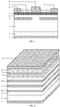
FIG. 1 is a front cross-sectional view of an exemplary vertical heterojunction semiconductor device. -
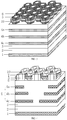
FIG. 2 is a perspective view of a heterojunction semiconductor device with low on-resistance according toEmbodiment 1. -
FIG. 3 is a simplified perspective view of the heterojunction semiconductor device with low on-resistance according toEmbodiment 1, in which portions of a passivation layer and a metal source electrode of the device are not shown. -
FIG. 4 is a simplified front sectional perspective view of the heterojunction semiconductor device with low on-resistance according toEmbodiment 1, in which the portions of the passivation layer and the metal source electrode of the device are not shown. -
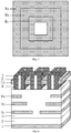
FIG. 5 is a front sectional view of the heterojunction semiconductor device with low on-resistance according toEmbodiment 1. -
FIG. 6 is a top sectional view of the heterojunction semiconductor device with low on-resistance according toEmbodiment 1, in which the portions of the passivation layer and the metal source electrode of the device are not shown. -
FIG. 7 is a top sectional view of a current blocking layer portion in a buffer layer of the heterojunction semiconductor device with low on-resistance according toEmbodiment 1. -
FIG. 8 illustrates a front sectional view of a heterojunction semiconductor device with low on-resistance according toEmbodiment 2 of which a gate structure is arranged in a matrix, in which portions of a passivation layer and a metal source electrode of the device are not shown. -
FIG. 9 is a simplified front sectional perspective view of a heterojunction semiconductor device with low on-resistance including a P-type gate according toEmbodiment 3, in which portions of a passivation layer and a metal source electrode of the device are not shown. -
FIG. 10 is a front sectional view of the heterojunction semiconductor device with low on-resistance shown inFIG. 9 . - In order to facilitate the understanding of the present disclosure, the present disclosure will be described more fully hereinafter with reference to the related accompanying drawings. Preferable embodiments of the present disclosure are presented in the accompanying drawings. However, the present disclosure may be embodied in many different forms and is not limited to the embodiments described herein. Rather, these embodiments are provided so that the understanding of the content of the present disclosure will be more thorough.
- All technical and scientific terms used herein have the same meaning as commonly understood by one of ordinary skill in the art to which this disclosure applies, unless otherwise defined. The terms used in the specification of present disclosure herein are for the purpose of describing specific embodiments only and are not intended to limit the present disclosure. The term "and/or" used herein includes any and all combinations of one or more of the associated listed items.
- It should be understood that, when an element or layer is described as being "on", "adjacent to", "connected to" or "coupled to" another element or layer, it can be directly on, adjacent to, connected to, or coupled to the other element or layer, or there can be an intermediate element. In contrast, when an element is described as being "directly on", "directly adjacent to", "directly connected to", or "directly coupled to" another element or layer, there is no intermediate element or layer. It should be understood that, although the terms of "first", "second", "third", and so on can be used to describe various elements, components, regions, layers and/or portions, these elements, components, regions, layers and/or portions should not be limited by these terms. These terms are merely used to distinguish an element, component, region, layer or portion from another element, component, region, layer or portion. Thus, the first element, component, region, layer or portion discussed below can be described as a second element, component, region, layer or portion without departing from the teachings of the present disclosure.
- Terms used herein are for the purpose of describing specific embodiments only and are not intended to be limiting of the present disclosure. As used herein, "a", "one" and "said/the" in singular forms are also intended to include a plural form unless the context clearly indicates other forms. It should also be understood that the terms "consist" and/or "include" when used in the description, determine presence of the features, integers, steps, operations, elements and/or components, but do not exclude the presence or addition of one or more other features, integers, steps, operations, elements, components, and/or groups. As used herein, the term "and/or" includes any and all combinations of related listed items.
- Solving the on-resistance problem of a vertical heterojunction semiconductor device is a very critical problem. An exemplary vertical GaN heterojunction semiconductor device is shown in
FIG. 1 , and its device structure mainly includes ametal drain electrode 1, asubstrate 2, aGaN buffer layer 3, aGaN pillar 5, anAlGaN layer 6, acurrent blocking layer 4, ametal source electrode 8, ametal gate electrode 10, and a passivation layer 11. When the device is on, current must flow through theGaN buffer layer 3. The exemplary vertical heterojunction semiconductor device has a significant contradiction between withstand voltage and on-resistance. - The present disclosure provides a heterojunction semiconductor device with low on-resistance, which includes:
- a metal drain electrode (1);
- a substrate (2) disposed on the metal drain electrode (1);
- a buffer layer (3) disposed on the substrate (2);
- a current blocking layer (4) disposed within the buffer layer (3);
- a heterojunction structure disposed on the buffer layer (3);
- a gate structure disposed on the buffer layer (3); and
- a metal source electrode (8) disposed on the buffer layer (3).
- The current blocking layer (4) includes a first-level annular current blocking layer (4a), a second-level annular current blocking layer (4b), and a third-level annular current blocking layer (4c), which are sequentially arranged from top to bottom, and symmetry centers of the annular current blocking layers are collinear. An annular inner opening of the first-level annular current blocking layer (4a) is larger than an annular inner opening of the second-level annular current blocking layer (4b), and the annular inner opening of the second-level annular current blocking layer (4b) is larger than an annular inner opening of the third-level annular current blocking layer (4c).
- The current blocking layer used in the present disclosure is divided into multilevel current blocking layers, where each level of the current blocking layers is distributed in a shape of a "hollow square" in the horizontal plane in which each level is located. The annular inner opening of each level of the current blocking layers becomes smaller level by level from top to bottom, and in addition, each level of the current blocking layers is distributed in a stepped shape in the buffer layer. The current blocking layer in the stepped shape can effectively improve the distribution of an electric field, so that a peak value of the electric field is far away from a channel and the average electric field is increased, thereby ensuring the withstand voltage capability of the device. The current blocking layer nearer to the GaN pillar has a larger annular inner opening, and the current entering the buffer layer through the channel is larger. With the increase of the number of levels of the current blocking layers, the annular inner openings become smaller. The depletion layer limits the flow path of the current, and the current can only flow through the minimum channel opening. As shown in
FIG. 8 , the electric field distribution diagrams of the current blocking layers with two types of "hollow square" distribution (a type that the annular inner openings become smaller level by level, and a type that the annular inner openings become larger level by level) are compared. The current blocking layers in the stepped shape with the annular inner openings becoming smaller level by level well limits the peak electric field to be far away from the GaN pillar side, and reduces the sacrifices to the forward current conduction capability of the device as much as possible while improving the withstand voltage capability of the device. In addition, an exemplary process of manufacturing a current blocking layer is Mg ion implantation. The Mg ion implantation will cause certain lattice damage, especially will cause a larger electric leakage to the current blocking layer. On the other hand, Mg has a strong memory effect, and has a large diffusion effect in a secondary epitaxy process. The area occupied by the current blocking layers in the stepped shape, especially the current blocking layer nearer to the GaN pillar, is smaller, which can reduce the effect of the Mg ion implantation on a channel layer and a barrier layer, and reduce the electric leakage while alleviating certain current collapse effect. - Embodiments of the present disclosure are further described below.
- Referring to
FIGS. 2-6 ,FIG. 4 shows a front sectional perspective view of a heterojunction semiconductor device with low on-resistance, andFIG. 5 shows a front sectional view of the heterojunction semiconductor device with low on-resistance. In this embodiment, the heterojunction semiconductor device with low on-resistance includes ametal drain electrode 1, asubstrate 2 disposed on themetal drain electrode 1, abuffer layer 3 disposed on thesubstrate 2, acurrent blocking layer 4 disposed within thebuffer layer 3, a gate structure disposed on thecurrent blocking layer 4 and including ametal gate electrode 10, ametal source electrode 8 disposed above themetal gate electrode 10, afirst passivation layer 11a disposed between themetal gate electrode 10 and themetal source electrode 8, and asecond passivation layer 11b disposed between themetal gate electrode 10 and thebuffer layer 3. Referring also toFIG. 7 , thecurrent blocking layer 4 includes a first-level annularcurrent blocking layer 4a, a second-level annularcurrent blocking layer 4b, and a third-level annularcurrent blocking layer 4c, which are sequentially arranged from top to bottom, and a symmetry center of each of the layers are collinear. An annular inner opening of the first-level annularcurrent blocking layer 4a is larger than an annular inner opening of the second-level annularcurrent blocking layer 4b, and an annular inner opening of the second-level annularcurrent blocking layer 4b is larger than an annular inner opening of the third-level annularcurrent blocking layer 4c, presenting a trend of becoming smaller level by level. - In this embodiment, the gate structure includes a
GaN pillar 5 standing on an upper surface of thebuffer layer 3, anAlGaN layer 6 wrapped on a side surface of theGaN pillar 5, and avertical channel 7 is formed at an interface between theGaN pillar 5 and theAlGaN layer 6 which are in contact with each other. Themetal gate electrode 10 is located on an outer side of theAlGaN layer 6, themetal source electrode 8 is located on upper surfaces of theGaN pillar 5 and theAlGaN layer 6, and a Schottky contact is formed between themetal source electrode 8 and theAlGaN layer 6. - The
current blocking layer 4 may include three levels, four levels, five levels or even more levels, and this embodiment employs three levels. In an embodiment in which thecurrent blocking layer 4 is of four levels, thecurrent blocking layer 4 further includes a fourth-level annular current blocking layer, a symmetry center of the fourth-level annular current blocking layer is collinear with the symmetry center of the third-level annularcurrent blocking layer 4c, and an annular inner opening of the fourth-level annular current blocking layer is smaller than the annular inner opening of the third-level annularcurrent blocking layer 4c. In an embodiment, each level of the current blocking layers are parallel to each other and are distributed in a stepped shape in thebuffer layer 3. - The
AlGaN layer 6 includes, but is not limited to, a hexagon in a horizontal cross-sectional shape, and includes any other polygonal structures or circular structures. TheGaN pillar 5 includes, but is not limited to, a circle in a horizontal cross-sectional shape, and includes any other polygonal structures. A cross section of theAlGaN layer 6 in this embodiment is in a regular hexagonal shape, and at least fourAlGaN layers 6 having N-type dopedGaN pillars 5 therein are disposed on the upper surface of thebuffer layer 3, and each of the AlGaN layers 6 are distributed and arranged in a honeycomb shape. - A vertical distance between a lower surface of the
metal gate electrode 10 and an upper surface of thebuffer layer 3 is 0.25-0.4 µm, and a thickness of themetal gate electrode 10 is 0.2 µm. - Referring to
FIG. 8 , as compared withEmbodiment 1, the gate structure of this embodiment is arranged and distributed in a matrix. The GaN pillars and the AlGaN layers are arranged and distributed in a matrix over the buffer layer, and the GaN pillars and the AlGaN layers are rectangular in horizontal cross-section. Other structures are the same as those ofEmbodiment 1. - Referring to
FIGS. 9 and 10 , as compared withEmbodiment 1, the gate structure of this embodiment is a P-type gate structure. AP-typeGaN cap layer 13 is present between themetal gate electrode 10 and theAlGaN layer 6, and other structures are the same as those ofEmbodiment 1. The P-type gate structure realizes a normally-off channel. - Compared with the prior art, the present disclosure has the following advantages.
- (1) In the present disclosure, the GaN pillar and the AlGaN layer are in contact with each other to form two-dimensional electron gas, which greatly reduce the required lateral occupied area of the device. In addition, the side wall of the GaN pillar and the AlGaN layer both have contact surfaces, and the GaN pillar is circular in the horizontal cross-section, so there is a current conduction path on the side wall of the GaN pillar, and the channel density is increased and the current capability is effectively improved, so that a higher on-state current is obtained when the device is on, thereby reducing the on-resistance of the device.
- (2) In the present disclosure, the GaN pillars and the AlGaN layers are distributed in a honeycomb shape on the upper surface of the buffer layer, which meets the requirements of the minimum size of the through-hole in the process requirements and can make maximum use of the lateral area of the device. A plurality of discrete GaN pillars exist on the buffer layer to generate a plurality of sections of channel currents, which effectively improves the current capability and enables a higher on-state current when the device is on, thereby reducing the on-resistance of the device.
- (3) The current blocking layer used in the present disclosure is divided into multilevel current blocking layers, where each level of the current blocking layers is distributed in a shape of a "hollow square" in the horizontal plane in which each level is located, and the annular inner openings become smaller level by level, and in addition, each level of the current blocking layers is parallel to each other and distributed in a stepped shape in the buffer layer. The current blocking layer in the stepped shape can effectively improve the distribution of the electric field, so that the peak value of the electric field is far away from the channel and the average electric field is increased, thereby ensuring the withstand voltage capability of the device. The current blocking layer nearer to the GaN pillar has a larger annular inner opening, and the current entering the buffer layer through the channel is larger. With the increase of the number of levels of the current blocking layers, the annular inner openings become smaller. The depletion layer limits the flow path of the current, and the current can only flow through the minimum channel opening. Through software simulation by the inventors, the electric field distribution diagrams of the current blocking layers with two types of "hollow square" distribution (a type that the annular inner openings become smaller level by level, and a type that the annular inner openings become larger level by level) are compared. The current blocking layers in the stepped shape with the annular inner openings becoming smaller level by level well limits the peak electric field to be far away from the GaN pillar side, and reduces the sacrifices to the forward current conduction capability of the device as much as possible while improving the withstand voltage capability of the device. In addition, an exemplary process of manufacturing a current blocking layer is Mg ion implantation. The Mg ion implantation will cause certain lattice damage, especially will cause a larger electric leakage to the current blocking layer. On the other hand, Mg has a strong memory effect, and has a large diffusion effect in the secondary epitaxy process. The area occupied by the current blocking layers in the stepped shape, especially the current blocking layer nearer to the GaN pillar, is smaller, which can reduce the effect of the Mg ion implantation on the channel layer and the barrier layer, and reduce the electric leakage while alleviating certain current collapse effect.
- (4) In the present disclosure, the vertical GaN pillar and the AlGaN layer are in contact with each other to form two-dimensional electron gas, the length of the channel is not affected by the lateral area of the device itself, the short-channel effect is overcome, so that the characteristic frequency of the device is significantly increased, and the advantage of higher operating frequency of the GaN material is fully exerted.
- (5) The exemplary heterojunction semiconductor structure has obvious current collapse phenomenon under high voltage. The present disclosure has a characteristic that the longitudinal channel and the substrate are not in the same direction, and the defects of the substrate portion have little influence on the device channel under high voltage. The structure of the present disclosure can effectively alleviate the current collapse effect.
- The aforementioned embodiments merely represent several embodiments of the present disclosure, and the description thereof is more specific and detailed, but they should not be construed as limiting the scope of the present disclosure. It should be noted that, several modifications and improvements may be made for those of ordinary skill in the art without departing from the concept of the present disclosure, and these are all within the protection scope of the present disclosure. Therefore, the protection scope of the present disclosure shall be subject to the appended claims.
Claims (15)
- A heterojunction semiconductor device with low on-resistance comprising: a metal drain electrode (1), a substrate (2) disposed on the metal drain electrode (1), a buffer layer (3) disposed on the substrate (2), a current blocking layer (4) disposed within the buffer layer (3), a gate structure disposed on the buffer layer (3) and comprising a metal gate electrode (10), a metal source electrode (8) disposed above the metal gate electrode (10), a first passivation layer (11a) disposed between the metal gate electrode (10) and the metal source electrode (8), and a second passivation layer (11b) disposed between the metal gate electrode (10) and the buffer layer (3); wherein the current blocking layer (4) comprises a first-level annular current blocking layer (4a), a second-level annular current blocking layer (4b), and a third-level annular current blocking layer (4c) which are sequentially arranged from top to bottom, and symmetry centers of each of the layers are collinear; an annular inner opening of the first-level annular current blocking layer (4a) is larger than an annular inner opening of the second-level annular current blocking layer (4b), and the annular inner opening of the second-level annular current blocking layer (4b) is larger than an annular inner opening of the third-level annular current blocking layer (4c), presenting a trend of becoming smaller level by level.
- The heterojunction semiconductor device with low on-resistance according to claim 1, wherein the gate structure comprises a GaN pillar (5) standing on an upper surface of the buffer layer (3), and an AlGaN layer (6) wrapped on a side surface of the GaN pillar (5), a vertical channel (7) being formed at an interface between the GaN pillar (5) and the AlGaN layer (6) in contact with each other; the metal gate electrode (10) is located on an outer side of the AlGaN layer (6), the metal source electrode (8) is located on upper surfaces of the GaN pillar (5) and the AlGaN layer (6), and a Schottky contact is formed between the metal source electrode (8) and the AlGaN layer (6).
- The heterojunction semiconductor device with low on-resistance according to claim 1, wherein the current blocking layer (4) further comprises a fourth-level annular current blocking layer, a symmetry center of the fourth-level annular current blocking layer is collinear with the symmetry center of the third-level annular current blocking layer (4c), and an annular inner opening of the fourth-level annular current blocking layer is smaller than the annular inner opening of the third-level annular current blocking layer (4c).
- The heterojunction semiconductor device with low on-resistance according to claim 2, wherein a cross section of the AlGaN layer (6) is in a regular hexagonal shape, and at least four AlGaN layers (6) having N-type doped GaN pillars (5) therein are disposed on the upper surface of the buffer layer (3) and are distributed and arranged in a honeycomb shape.
- The heterojunction semiconductor device with low on-resistance according to claim 1, wherein a vertical distance between a lower surface of the metal gate electrode (10) and an upper surface of the buffer layer (3) is 0.25 µm to 0.4 µm, and a thickness of the metal gate electrode (10) is 0.2 µm.
- A heterojunction semiconductor device with low on-resistance, comprising:a metal drain electrode (1);a substrate (2) disposed on the metal drain electrode (1);a buffer layer (3) disposed on the substrate (2);a current blocking layer (4) disposed within the buffer layer (3);a heterojunction structure disposed on the buffer layer (3);a gate structure disposed on the buffer layer (3); anda metal source electrode (8) disposed on the buffer layer (3);wherein, the current blocking layer (4) comprises a first-level annular current blocking layer (4a), a second-level annular current blocking layer (4b), and a third-level annular current blocking layer (4c) which are sequentially arranged from top to bottom, and symmetry centers of each of the annular current blocking layers are collinear; an annular inner opening of the first-level annular current blocking layer (4a) is larger than an annular inner opening of the second-level annular current blocking layer (4b), and the annular inner opening of the second-level annular current blocking layer (4b) is larger than an annular inner opening of the third-level annular current blocking layer (4c).
- The heterojunction semiconductor device with low on-resistance according to claim 6, wherein the gate structure further comprises:a GaN pillar (5) standing on an upper surface of the buffer layer (3);an AlGaN layer (6) wrapping the GaN pillar (5) on a side surface of the GaN pillar (5), a vertical channel (7) being formed at an interface between the AlGaN layer (6) and the GaN pillar (5) in contact with each other; anda metal gate electrode (10) disposed on an outer side of the AlGaN layer (6);wherein the metal source electrode (8) is located above the metal gate electrode (10) and on upper surfaces of the GaN pillar (5) and the AlGaN layer (6), and a Schottky contact is formed between the metal source electrode (8) and the AlGaN layer (6).
- The heterojunction semiconductor device with low on-resistance according to claim 7, further comprising:a first passivation layer (11a) disposed between the metal gate electrode (10) and the metal source electrode (8); anda second passivation layer (11b) disposed between the metal gate electrode (10) and the buffer layer (3).
- The heterojunction semiconductor device with low on-resistance according to claim 7, wherein a cross section of the AlGaN layer (6) is in a regular hexagonal shape, and at least four AlGaN layers (6) having GaN pillars (5) therein are disposed on the upper surface of the buffer layer (3), and each of the AlGaN layers (6) are distributed and arranged in a honeycomb shape.
- The heterojunction semiconductor device with low on-resistance according to claim 9, wherein the GaN pillars (5) are N-type doped GaN pillars.
- The heterojunction semiconductor device with low on-resistance according to claim 7, wherein the GaN pillars (5) and the AlGaN layers (6) are arranged in a matrix over the buffer layer (3), and the GaN pillars (5) and the AlGaN layers (6) are rectangular in horizontal cross-section.
- The heterojunction semiconductor device with low on-resistance according to claim 7, wherein the gate structure further comprises a P-type doped GaN cap layer (13) disposed between the metal gate electrode (10) and the AlGaN layer (6).
- The heterojunction semiconductor device with low on-resistance according to claim 7, wherein a vertical distance between a lower surface of the metal gate electrode (10) and an upper surface of the buffer layer (3) is 0.25 µm to 0.4 µm, and a thickness of the metal gate electrode (10) is 0.2 µm.
- The heterojunction semiconductor device with low on-resistance according to claim 6, wherein the current blocking layer (4) is formed by Mg ion implantation.
- The heterojunction semiconductor device with low on-resistance according to claim 6, wherein the current blocking layer (4) further comprises a fourth-level annular current blocking layer located below the third-level annular current blocking layer (4c), a symmetry center of the fourth-level annular current blocking layer is collinear with the symmetry center of the third-level annular current blocking layer (4c), and an annular inner opening of the fourth-level annular current blocking layer is smaller than the annular inner opening of the third-level annular current blocking layer (4c).
Applications Claiming Priority (2)
| Application Number | Priority Date | Filing Date | Title |
|---|---|---|---|
| CN201811585004.5A CN111354777A (en) | 2018-12-24 | 2018-12-24 | Heterojunction semiconductor device with low on-resistance |
| PCT/CN2019/126517 WO2020135207A1 (en) | 2018-12-24 | 2019-12-19 | Heterojunction semiconductor device with low on-resistance |
Publications (2)
| Publication Number | Publication Date |
|---|---|
| EP3905339A1 true EP3905339A1 (en) | 2021-11-03 |
| EP3905339A4 EP3905339A4 (en) | 2022-09-28 |
Family
ID=71126336
Family Applications (1)
| Application Number | Title | Priority Date | Filing Date |
|---|---|---|---|
| EP19904187.2A Pending EP3905339A4 (en) | 2018-12-24 | 2019-12-19 | HETEROJUNCTION SEMICONDUCTOR DEVICE HAVING LOW ON-STATE RESISTANCE |
Country Status (5)
| Country | Link |
|---|---|
| US (1) | US12224340B2 (en) |
| EP (1) | EP3905339A4 (en) |
| JP (1) | JP7273971B2 (en) |
| CN (1) | CN111354777A (en) |
| WO (1) | WO2020135207A1 (en) |
Cited By (1)
| Publication number | Priority date | Publication date | Assignee | Title |
|---|---|---|---|---|
| CN114725194A (en) * | 2022-02-17 | 2022-07-08 | 西安电子科技大学 | Low-voltage terminal device based on field modulation under grid and preparation method thereof |
Families Citing this family (2)
| Publication number | Priority date | Publication date | Assignee | Title |
|---|---|---|---|---|
| CN113871316A (en) * | 2021-09-26 | 2021-12-31 | 浙江里阳半导体有限公司 | Method for detecting vapor deposition defects of semiconductor device |
| CN120812961B (en) * | 2025-09-11 | 2025-11-21 | 恒泰柯半导体(上海)有限公司 | Methods and systems for reducing the on-resistance of Schottky diodes |
Family Cites Families (30)
| Publication number | Priority date | Publication date | Assignee | Title |
|---|---|---|---|---|
| US6181723B1 (en) * | 1997-05-07 | 2001-01-30 | Sharp Kabushiki Kaisha | Semiconductor light emitting device with both carbon and group II element atoms as p-type dopants and method for producing the same |
| US7098093B2 (en) * | 2004-09-13 | 2006-08-29 | Northrop Grumman Corporation | HEMT device and method of making |
| JP4189415B2 (en) * | 2006-06-30 | 2008-12-03 | 株式会社東芝 | Semiconductor device |
| JP5208463B2 (en) * | 2007-08-09 | 2013-06-12 | ローム株式会社 | Nitride semiconductor device and method for manufacturing nitride semiconductor device |
| US7772621B2 (en) * | 2007-09-20 | 2010-08-10 | Infineon Technologies Austria Ag | Semiconductor device with structured current spread region and method |
| US8188513B2 (en) * | 2007-10-04 | 2012-05-29 | Stc.Unm | Nanowire and larger GaN based HEMTS |
| JP4737471B2 (en) | 2009-10-08 | 2011-08-03 | 住友電気工業株式会社 | Semiconductor device and manufacturing method thereof |
| JP2011142200A (en) * | 2010-01-07 | 2011-07-21 | Toyota Central R&D Labs Inc | Field effect transistor |
| CN103026491B (en) * | 2010-07-06 | 2016-03-02 | 香港科技大学 | Normally-off Group III Nitride Metal-Two-Dimensional Electron Gas Tunneling Junction Field Effect Transistor |
| JP2012156250A (en) * | 2011-01-25 | 2012-08-16 | Toyota Motor Corp | Semiconductor device including p-type group iii nitride semiconductor layer, and method for manufacturing the same |
| JP2012156253A (en) * | 2011-01-25 | 2012-08-16 | Sumitomo Electric Ind Ltd | Manufacturing method of nitride semiconductor element |
| JP2011135094A (en) * | 2011-02-25 | 2011-07-07 | Sumitomo Electric Ind Ltd | Semiconductor device, and method of manufacturing the same |
| CN102881716A (en) * | 2012-09-27 | 2013-01-16 | 电子科技大学 | Field-induced tunneling enhanced HEMT (high electron mobility transistor) device |
| CN102945859A (en) * | 2012-11-07 | 2013-02-27 | 电子科技大学 | GaN heterojunction HEMT (High Electron Mobility Transistor) device |
| EP2884538A1 (en) * | 2013-12-16 | 2015-06-17 | ABB Technology AB | Power semiconductor device |
| CN104167442B (en) * | 2014-08-29 | 2017-04-12 | 电子科技大学 | Vertical GaN heterojunction field-effect transistor with P type GaN island |
| JP6665157B2 (en) * | 2015-03-17 | 2020-03-13 | パナソニック株式会社 | Nitride semiconductor device |
| CN104992971B (en) * | 2015-06-29 | 2020-01-24 | 电子科技大学 | Vertical gallium nitride based heterojunction field effect transistor with composite low-K current barrier layer |
| CN105304707A (en) * | 2015-10-28 | 2016-02-03 | 电子科技大学 | Enhanced HEMT device |
| CN105762078B (en) * | 2016-05-06 | 2018-11-16 | 西安电子科技大学 | GaN base nano-channel high electron mobility transistor and production method |
| CN105845724B (en) * | 2016-06-17 | 2019-03-29 | 电子科技大学 | A kind of vertical HEMT device of accumulation type |
| CN106340535A (en) * | 2016-08-01 | 2017-01-18 | 苏州捷芯威半导体有限公司 | Semiconductor device and manufacturing method thereof |
| US10418475B2 (en) * | 2016-11-28 | 2019-09-17 | Arizona Board Of Regents On Behalf Of Arizona State University | Diamond based current aperture vertical transistor and methods of making and using the same |
| CN107170820B (en) * | 2017-03-29 | 2020-04-14 | 西安电子科技大学 | Arc Gate-Drain Compound Field Plate Current Aperture Heterojunction Devices |
| CN107146811B (en) * | 2017-03-29 | 2019-12-10 | 西安电子科技大学 | current aperture power transistor based on barrier layer modulation structure and manufacturing method thereof |
| CN107154435B (en) * | 2017-03-29 | 2019-10-08 | 西安电子科技大学 | Grading current barrier layer vertical-type power device |
| CN111886683B (en) * | 2018-03-22 | 2024-01-02 | 松下控股株式会社 | Nitride semiconductor device |
| CN108598163A (en) * | 2018-05-14 | 2018-09-28 | 电子科技大学 | A kind of GaN hetero-junctions longitudinal direction power device |
| CN108649070A (en) * | 2018-05-14 | 2018-10-12 | 电子科技大学 | A kind of GaN hetero-junctions conductance modulation field-effect tube |
| US10741494B2 (en) * | 2018-11-07 | 2020-08-11 | Semiconductor Components Industries, Llc | Electronic device including a contact structure contacting a layer |
-
2018
- 2018-12-24 CN CN201811585004.5A patent/CN111354777A/en active Pending
-
2019
- 2019-12-19 WO PCT/CN2019/126517 patent/WO2020135207A1/en not_active Ceased
- 2019-12-19 US US17/417,663 patent/US12224340B2/en active Active
- 2019-12-19 JP JP2021536808A patent/JP7273971B2/en active Active
- 2019-12-19 EP EP19904187.2A patent/EP3905339A4/en active Pending
Cited By (1)
| Publication number | Priority date | Publication date | Assignee | Title |
|---|---|---|---|---|
| CN114725194A (en) * | 2022-02-17 | 2022-07-08 | 西安电子科技大学 | Low-voltage terminal device based on field modulation under grid and preparation method thereof |
Also Published As
| Publication number | Publication date |
|---|---|
| CN111354777A (en) | 2020-06-30 |
| JP2022515428A (en) | 2022-02-18 |
| US20220069115A1 (en) | 2022-03-03 |
| EP3905339A4 (en) | 2022-09-28 |
| US12224340B2 (en) | 2025-02-11 |
| JP7273971B2 (en) | 2023-05-15 |
| WO2020135207A1 (en) | 2020-07-02 |
Similar Documents
| Publication | Publication Date | Title |
|---|---|---|
| US10157986B2 (en) | Silicon carbide semiconductor device and method for manufacturing same | |
| KR101620717B1 (en) | Insulated gate bipolar transistor with mesa sections between cell trench structures and method of manufacturing | |
| US9087893B2 (en) | Superjunction semiconductor device with reduced switching loss | |
| KR100290693B1 (en) | Power semiconductor element controllable by field effect | |
| JP6214680B2 (en) | Silicon carbide semiconductor device | |
| US12224340B2 (en) | Heterojunction semiconductor device with low on-resistance | |
| CN105845724A (en) | Accumulation vertical HEMT device | |
| JP4865260B2 (en) | Semiconductor device | |
| CN117558761A (en) | A wide bandgap semiconductor trench MOSFET device and its manufacturing method | |
| US6515330B1 (en) | Power device having vertical current path with enhanced pinch-off for current limiting | |
| EP3025373B1 (en) | Mos-bipolar device | |
| CN107431090A (en) | Power semiconductor device | |
| KR20250142282A (en) | Schottky barrier diode | |
| CN120957445A (en) | A high-reliability superjunction trench gate silicon carbide VDMOS with voltages above 3kV and its fabrication method | |
| KR20080095764A (en) | Semiconductor devices | |
| JP7471403B2 (en) | Vertical field effect transistor and method for forming same | |
| US6201280B1 (en) | Transistor of SIC | |
| CN112885901B (en) | High electron mobility transistor and method of forming the same | |
| CN116960155A (en) | A well-type trench VDMOSFET structure with increased source contact in the JFET region | |
| JP7354868B2 (en) | switching element | |
| US20240297223A1 (en) | Silicon carbide semiconductor device | |
| US20260006870A1 (en) | Semiconductor device and manufacturing method | |
| CN114586174B (en) | Vertical field effect transistor and method for the construction thereof | |
| JP2026000754A (en) | Semiconductor Devices | |
| KR20230109462A (en) | Pillar strucutre and super junction semiconductor device including the same |
Legal Events
| Date | Code | Title | Description |
|---|---|---|---|
| STAA | Information on the status of an ep patent application or granted ep patent |
Free format text: STATUS: THE INTERNATIONAL PUBLICATION HAS BEEN MADE |
|
| PUAI | Public reference made under article 153(3) epc to a published international application that has entered the european phase |
Free format text: ORIGINAL CODE: 0009012 |
|
| STAA | Information on the status of an ep patent application or granted ep patent |
Free format text: STATUS: REQUEST FOR EXAMINATION WAS MADE |
|
| 17P | Request for examination filed |
Effective date: 20210625 |
|
| AK | Designated contracting states |
Kind code of ref document: A1 Designated state(s): AL AT BE BG CH CY CZ DE DK EE ES FI FR GB GR HR HU IE IS IT LI LT LU LV MC MK MT NL NO PL PT RO RS SE SI SK SM TR |
|
| DAV | Request for validation of the european patent (deleted) | ||
| DAX | Request for extension of the european patent (deleted) | ||
| A4 | Supplementary search report drawn up and despatched |
Effective date: 20220826 |
|
| RIC1 | Information provided on ipc code assigned before grant |
Ipc: H01L 29/20 20060101ALN20220822BHEP Ipc: H01L 29/10 20060101ALN20220822BHEP Ipc: H01L 29/06 20060101ALI20220822BHEP Ipc: H01L 29/778 20060101AFI20220822BHEP |
|
| STAA | Information on the status of an ep patent application or granted ep patent |
Free format text: STATUS: EXAMINATION IS IN PROGRESS |
|
| 17Q | First examination report despatched |
Effective date: 20250612 |