EP3904902B1 - Multi-layer phased array lidar transmission chip, manufacturing method, and lidar - Google Patents
Multi-layer phased array lidar transmission chip, manufacturing method, and lidar Download PDFInfo
- Publication number
- EP3904902B1 EP3904902B1 EP19890176.1A EP19890176A EP3904902B1 EP 3904902 B1 EP3904902 B1 EP 3904902B1 EP 19890176 A EP19890176 A EP 19890176A EP 3904902 B1 EP3904902 B1 EP 3904902B1
- Authority
- EP
- European Patent Office
- Prior art keywords
- layer
- silicon
- structure layer
- soi
- phased array
- Prior art date
- Legal status (The legal status is an assumption and is not a legal conclusion. Google has not performed a legal analysis and makes no representation as to the accuracy of the status listed.)
- Active
Links
Images


Classifications
-
- G—PHYSICS
- G01—MEASURING; TESTING
- G01S—RADIO DIRECTION-FINDING; RADIO NAVIGATION; DETERMINING DISTANCE OR VELOCITY BY USE OF RADIO WAVES; LOCATING OR PRESENCE-DETECTING BY USE OF THE REFLECTION OR RERADIATION OF RADIO WAVES; ANALOGOUS ARRANGEMENTS USING OTHER WAVES
- G01S7/00—Details of systems according to groups G01S13/00, G01S15/00, G01S17/00
- G01S7/48—Details of systems according to groups G01S13/00, G01S15/00, G01S17/00 of systems according to group G01S17/00
- G01S7/481—Constructional features, e.g. arrangements of optical elements
-
- G—PHYSICS
- G01—MEASURING; TESTING
- G01S—RADIO DIRECTION-FINDING; RADIO NAVIGATION; DETERMINING DISTANCE OR VELOCITY BY USE OF RADIO WAVES; LOCATING OR PRESENCE-DETECTING BY USE OF THE REFLECTION OR RERADIATION OF RADIO WAVES; ANALOGOUS ARRANGEMENTS USING OTHER WAVES
- G01S7/00—Details of systems according to groups G01S13/00, G01S15/00, G01S17/00
- G01S7/48—Details of systems according to groups G01S13/00, G01S15/00, G01S17/00 of systems according to group G01S17/00
- G01S7/481—Constructional features, e.g. arrangements of optical elements
- G01S7/4814—Constructional features, e.g. arrangements of optical elements of transmitters alone
-
- G—PHYSICS
- G01—MEASURING; TESTING
- G01S—RADIO DIRECTION-FINDING; RADIO NAVIGATION; DETERMINING DISTANCE OR VELOCITY BY USE OF RADIO WAVES; LOCATING OR PRESENCE-DETECTING BY USE OF THE REFLECTION OR RERADIATION OF RADIO WAVES; ANALOGOUS ARRANGEMENTS USING OTHER WAVES
- G01S7/00—Details of systems according to groups G01S13/00, G01S15/00, G01S17/00
- G01S7/48—Details of systems according to groups G01S13/00, G01S15/00, G01S17/00 of systems according to group G01S17/00
- G01S7/481—Constructional features, e.g. arrangements of optical elements
- G01S7/4818—Constructional features, e.g. arrangements of optical elements using optical fibres
-
- G—PHYSICS
- G01—MEASURING; TESTING
- G01S—RADIO DIRECTION-FINDING; RADIO NAVIGATION; DETERMINING DISTANCE OR VELOCITY BY USE OF RADIO WAVES; LOCATING OR PRESENCE-DETECTING BY USE OF THE REFLECTION OR RERADIATION OF RADIO WAVES; ANALOGOUS ARRANGEMENTS USING OTHER WAVES
- G01S7/00—Details of systems according to groups G01S13/00, G01S15/00, G01S17/00
- G01S7/48—Details of systems according to groups G01S13/00, G01S15/00, G01S17/00 of systems according to group G01S17/00
- G01S7/483—Details of pulse systems
- G01S7/484—Transmitters
-
- G—PHYSICS
- G02—OPTICS
- G02F—OPTICAL DEVICES OR ARRANGEMENTS FOR THE CONTROL OF LIGHT BY MODIFICATION OF THE OPTICAL PROPERTIES OF THE MEDIA OF THE ELEMENTS INVOLVED THEREIN; NON-LINEAR OPTICS; FREQUENCY-CHANGING OF LIGHT; OPTICAL LOGIC ELEMENTS; OPTICAL ANALOGUE/DIGITAL CONVERTERS
- G02F1/00—Devices or arrangements for the control of the intensity, colour, phase, polarisation or direction of light arriving from an independent light source, e.g. switching, gating or modulating; Non-linear optics
- G02F1/01—Devices or arrangements for the control of the intensity, colour, phase, polarisation or direction of light arriving from an independent light source, e.g. switching, gating or modulating; Non-linear optics for the control of the intensity, phase, polarisation or colour
- G02F1/015—Devices or arrangements for the control of the intensity, colour, phase, polarisation or direction of light arriving from an independent light source, e.g. switching, gating or modulating; Non-linear optics for the control of the intensity, phase, polarisation or colour based on semiconductor elements having potential barriers, e.g. having a PN or PIN junction
-
- G—PHYSICS
- G02—OPTICS
- G02F—OPTICAL DEVICES OR ARRANGEMENTS FOR THE CONTROL OF LIGHT BY MODIFICATION OF THE OPTICAL PROPERTIES OF THE MEDIA OF THE ELEMENTS INVOLVED THEREIN; NON-LINEAR OPTICS; FREQUENCY-CHANGING OF LIGHT; OPTICAL LOGIC ELEMENTS; OPTICAL ANALOGUE/DIGITAL CONVERTERS
- G02F1/00—Devices or arrangements for the control of the intensity, colour, phase, polarisation or direction of light arriving from an independent light source, e.g. switching, gating or modulating; Non-linear optics
- G02F1/29—Devices or arrangements for the control of the intensity, colour, phase, polarisation or direction of light arriving from an independent light source, e.g. switching, gating or modulating; Non-linear optics for the control of the position or the direction of light beams, i.e. deflection
- G02F1/292—Devices or arrangements for the control of the intensity, colour, phase, polarisation or direction of light arriving from an independent light source, e.g. switching, gating or modulating; Non-linear optics for the control of the position or the direction of light beams, i.e. deflection by controlled diffraction or phased-array beam steering
-
- G—PHYSICS
- G02—OPTICS
- G02B—OPTICAL ELEMENTS, SYSTEMS OR APPARATUS
- G02B6/00—Light guides; Structural details of arrangements comprising light guides and other optical elements, e.g. couplings
- G02B6/10—Light guides; Structural details of arrangements comprising light guides and other optical elements, e.g. couplings of the optical waveguide type
- G02B6/12—Light guides; Structural details of arrangements comprising light guides and other optical elements, e.g. couplings of the optical waveguide type of the integrated circuit kind
- G02B2006/12035—Materials
- G02B2006/12061—Silicon
-
- G—PHYSICS
- G02—OPTICS
- G02B—OPTICAL ELEMENTS, SYSTEMS OR APPARATUS
- G02B6/00—Light guides; Structural details of arrangements comprising light guides and other optical elements, e.g. couplings
- G02B6/10—Light guides; Structural details of arrangements comprising light guides and other optical elements, e.g. couplings of the optical waveguide type
- G02B6/12—Light guides; Structural details of arrangements comprising light guides and other optical elements, e.g. couplings of the optical waveguide type of the integrated circuit kind
- G02B6/122—Basic optical elements, e.g. light-guiding paths
- G02B6/125—Bends, branchings or intersections
Definitions
- the present disclosure relates to the field of light detection and ranging (LiDAR) technologies and, in particular, to a phased array LiDAR transmitting chip of multi-layer materials, a manufacturing method thereof, and a LiDAR device.
- LiDAR light detection and ranging
- phased array LiDAR has been proposed for a long time, and various design schemes are also being developed.
- Current phased array LiDAR chips use silicon on insulator (SOI) material as a substrate, and make use of the characteristics of silicon to fabricate various on-chip structures, thus realizing basic functions of LiDAR.
- SOI silicon on insulator
- silicon has its own shortcomings. Since silicon is a strongly nonlinear material with a strong two-photon absorption effect and a free carrier absorption effect, and its low-order nonlinear refractive index is very large, making it difficult to transmit high-power light in a silicon waveguide with low loss, which greatly limits the optical power input to the phased array LiDAR transmitting chip, and seriously affects the detection performance of the LiDAR and brings great pressure to the signal detection part.
- CHUNG SUNGWON ET AL "A Monolithically Integrated Large-Scale Optical Phased Array in Silicon-on-Insulator CMOS", IEEE JOURNAL OF SOLID-STATE CIRCUITS, IEEE, USA, vol. 53, no. 1, 18 October 2017 (2017-10-18), pages 275 - 296 , discloses that a large-scale monolithic silicon nanophotonic phased array on a chip creates and dynamically steers a high-resolution optical beam in free space, enabling emerging applications in sensing, imaging, and communication.
- the scalable architecture leverages sub-array structure, mitigating the impact of process variation on the phased array performance.
- sharing control electronics among multiple optical modulators in the scalable architecture reduces the number of digital-to-analog converters (DACs) required for an N 2 array from O( N 2 ) to O(N), allowing a small silicon footprint.
- An optical phased array for 1550-nm wavelength with 1024 uniformly spaced optical grating antennas, 1192 optical variable phase shifters, and 168 optical variable attenuators is integrated into a 5.7 mm ⁇ 6.4 mm chip in a commercial 180-nm silicon-on-insulator RF CMOS technology.
- the control signals for the optical variable phase shifters and attenuators are provided by 136 DACs with 14-bit nonuniform resolution using 2.5-V input-output transistors.
- the implemented phased array can create 0.03° narrow optical beams that can be steered unambiguously within ⁇ 22.5°.
- NOTAROS JELENA ET AL "CMOS-Compatible Optical Phased Arrays with Monolithically-Integrated Erbium Lasers", 2018 CONFERENCE ON LASERS AND ELECTRO-OPTICS (CLEO), OSA, 13 May 2018 (2018-05-13), pages 1 - 2 , discloses that an electronically-steerable integrated optical phased array powered by an on-chip erbium-doped laser is experimentally demonstrated. This system represents the first demonstration of a rare-earth-doped laser monolithically integrated with an active CMOS-compatible silicon photonics system.
- Embodiments of the present disclosure provides a phased array LiDAR transmitting chip of multi-layer materials, a manufacturing method thereof, and a LiDAR device, solving the power limit problem of a phased array LiDAR chip in the prior art, so that the optical power input into the phased array LiDAR transmitting chip may be greatly increased, thus greatly improving the detection performance of LiDAR, and reducing a great deal of pressure on the signal detection part.
- the invention is set out in the appended set of claims.
- an embodiment of the present disclosure provides a phased array LiDAR transmitting chip of multi-layer materials, including: a first material structure layer, an SOI silicon waveguide structure layer, and a coupling connection structure, the first material structure layer including: an input coupler and a beam splitter;
- the SOI silicon waveguide structure layer includes: phase modulators and an optical antenna;
- the first material coupling waveguides and the silicon coupling waveguides have a tip width of 100 nm to 300 nm;
- the first material structure layer further includes a first material backbone waveguide; the input coupler is optically connected to the beam splitter through the first material backbone waveguide.
- an embodiment of the present disclosure provides a phased array LiDAR device, including the phased array LiDAR transmitting chip of multi-layer materials according to any implementation of the first aspect described above.
- the forming an SOI silicon waveguide structure layer in a first region above a top silicon layer of an SOI substrate includes: transferring a first waveguide pattern to the top silicon layer of the SOI substrate by using an electron beam exposure process or a stepper lithography process, and forming the SOI silicon waveguide structure layer in the first region by using an inductively coupled plasma (ICP) etching process.
- ICP inductively coupled plasma
- the SOI silicon waveguide structure layer in the first region above the top silicon layer of the SOI substrate further includes:
- Embodiments of the present disclosure provide a phased array LiDAR transmitting chip of multi-layer materials, a manufacturing method thereof, and a LiDAR device.
- the phased array LiDAR transmitting chip of multi-layer materials includes: a first material structure layer, a SOI silicon waveguide structure layer, and a coupling connection structure.
- the first material structure layer includes an input coupler and a beam splitter; the input coupler is optically connected to the beam splitter; the beam splitter is optically connected to the SOI silicon waveguide structure layer through the coupling connection structure; the input coupler is configured to couple input light into the chip; the beam splitter is configured to split a light wave coupled into the chip; the coupling connection structure is configured to couple each of the split light waves into a silicon waveguide corresponding to the SOI silicon waveguide structure layer; where the non-linear refractive index of the first material in the first material structure layer is lower than the non-linear refractive index of a silicon material, and the first material is compatible with a CMOS process.
- the input coupler in the first material structure layer may couple a high-power light wave to the chip, and then divide the light wave into several light waves through the beam splitter, so as to reduce the optical power in each of first material waveguides, and enable the optical power in each of the first material waveguides to satisfy normal transmission in the silicon waveguide.
- the optical power input into the phased array LiDAR transmitting chip of multi-layer materials may be greatly increased, thus greatly improving the detection performance of LiDAR, and reducing a lot of pressure on the signal detection part.
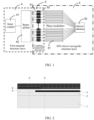
- FIG. 1 is a structure diagram of a phased array LiDAR transmitting chip of multi-layer materials according to a first embodiment of the present disclosure.
- the phased array LiDAR transmitting chip of multi-layer materials provided in this embodiment includes: a first material structure layer 4, an SOI silicon waveguide structure layer 3, and a coupling connection structure 5, and the first material structure layer 4 includes an input coupler 41 and a beam splitter 42.
- the input coupler 41 is optically connected to the beam splitter 42; the beam splitter 42 is optically connected to the SOI silicon waveguide structure layer 3 through the coupling connection structure 5.
- the input coupler 41 is configured to couple input light to the chip.
- the beam splitter 42 is configured to split a light wave coupled to the chip.
- the coupling connection structure 5 is configured to couple each of the split light waves to a corresponding silicon waveguide in the SOI silicon waveguide structure layer 3.
- the non-linear refractive index of a first material in the first material structure layer 4 is lower than the non-linear refractive index of a silicon material, and the first material is compatible with a complementary metal oxide semiconductor (CMOS) process.
- CMOS complementary metal oxide semiconductor
- non-linear refractive index refers to low-order non-linear refractive indexes.
- the low-order non-linear refractive indexes may also be the first-order non-linear refractive index, the second-order non-linear refractive index, the third-order non-linear refractive index, etc.
- the phased array LiDAR transmitting chip of multi-layer materials is integrated on an SOI substrate satisfying the CMOS process.
- the SOI substrate includes a substrate silicon layer 1, a buried oxide layer 2 and a top silicon layer 21 from bottom to top.
- the material and thickness of each layer of the SOI substrate are not limited in this embodiment.
- the material and thickness of each layer may be customized according to different needs, or a conventional standard CMOS process SOI substrate product may be used.
- the material of the substrate silicon layer 1 is silicon with a thickness of 500 ⁇ m to 600 ⁇ m.
- the material of the buried oxide layer 2 is silicon dioxide with a thickness of 2 ⁇ m
- the material of the top silicon layer 21 is silicon with a thickness of 220 nm or 340 nm.
- silicon has a large low-order non-linear refractive index, and the silicon material exhibits a strong two-photon absorption effect and free carrier absorption effect, so generally the optical power allowed to be transmitted in silicon waveguides is very small, usually about 100 mw. This makes a conventional pure silicon-based phased array LiDAR transmitting chip unable to achieve on-chip processing and emission of high-power lasers, which seriously reduces the detection performance of the LiDAR.
- the first material structure layer 4 having a lower nonlinear refractive index than the nonlinear refractive index of a silicon material is used.
- the first material structure layer 4 includes multiple forms of first material waveguides therein to form the input coupler 41 and the beam splitter 42.
- the first material in the first material structure layer 4 is compatible with the CMOS process.
- the first material may be a silicon-like material, such as silicon nitride or silicon oxynitride. Therefore, the input coupler 41 in the first material structure layer 4 is configured to couple light waves to the chip and may couple high-power input light to the first material structure layer 4.
- the size of the input coupler 41 of the first material is enabled to be larger than the size of a silicon input coupler in the prior art. Therefore, the mismatch between the spot size of the input coupler 41 and the fiber spot size may be greatly reduced, and the coupling efficiency may be effectively improved.
- the input coupler 41 of the first material may achieve a higher coupling efficiency than the silicon input coupler in the prior art.
- the first material is not easily affected by two-photon absorption effect and carrier absorption effect, and its first order nonlinear refractive index is nearly 20 times smaller than the first order nonlinear refractive index of silicon, enabling light waves of optical power that is much higher than optical power transmitted in the silicon waveguide to be transmitted in the waveguide of the first material structure layer 4.
- the beam splitter 42 is configured to split a light wave coupled to the chip, the light wave coupled to the input coupler 41, after passing through the beam splitter 42, is divided into several light waves so that the optical power in each of the first material waveguides after beam-splitting by the beam splitter 42 is much smaller.
- optical power of each of the light waves may satisfy that after being normally transmitted in the silicon waveguide, then each of the light waves is coupled to the a corresponding silicon waveguide in the SOI silicon waveguide structure 3 through the coupling connection structure 5.
- the phased array LiDAR transmitting chip of multi-layer materials includes: a first material structure layer 4, an SOI silicon waveguide structure layer 3, and a coupling connection structure 5, and the first material structure layer 4 includes an input coupler 41 and a beam splitter 42; the input coupler 41 is optically connected to the beam splitter 42; the beam splitter 42 is optically connected to the SOI silicon waveguide structure layer 3 through the coupling connection structure 5; the input coupler 41 is configured to couple input light to the chip; the beam splitter 42 is configured to split the light wave coupled to the chip; the coupling connection structure 5 is configured to couple each of the split light waves to a corresponding silicon waveguide in the SOI silicon waveguide structure layer 3; where the non-linear refractive index of a first material in the first material structure layer 4 is lower than the non-linear refractive index of a silicon material and the first material is compatible with a CMOS process.
- the input coupler 41 in the first material structure layer 4 may couple a high-power light wave into the chip, and then divide the light wave into several light waves through the beam splitter 42, so as to reduce the optical power in each of the first material waveguides and enable the optical power in each of the first material waveguides to be able to satisfy normal transmission in the silicon waveguide.
- the optical power input into the phased array LiDAR transmitting chip of multi-layer materials may be greatly increased, thus greatly improving the detection performance of LiDAR, and reducing a lot of pressure on the signal detection part.
- the SOI silicon waveguide structure layer 3 includes: phase modulators 31 and an optical antenna 32.
- phase modulators 31 and the optical antenna 32 are connected through silicon waveguides.
- phase modulators 31 are configured to change the phase of a light wave coupled to a corresponding silicon waveguide in the SOI silicon waveguide structure layer 3.
- the optical antenna 32 is configured to transmit phase-changed light waves in the silicon waveguides into space.
- the phase modulators 31 and the optical antenna 32 are optically connected through silicon waveguides.
- the phase modulators 31 forms an electrode with a silicon waveguide and adjusts the refractive index of the silicon waveguide by applying current or voltage bias, thus changing the phase of the light wave in each waveguide.
- the light waves in the silicon waveguides are phase-adjusted by the phase modulators 31 and then transmitted by the silicon waveguides to the optical antenna 32 and emitted into space.
- the SOI silicon waveguide structure layer 3 includes phase modulators 31 and an optical antenna 32.
- the phase modulators and the optical antenna are connected through the silicon waveguides; the phase modulators 31 are configured to change the phase of a light wave coupled to a corresponding silicon waveguide in the SOI silicon waveguide structure layer 3.
- the optical antenna 32 is configured to transmit phase-changed light waves in the silicon waveguides into space. Therefore, the input high-power light to the phased array LiDAR transmitting chip of multi-layer material s may be emit into space, thus greatly improving the detection performance of LiDAR and reducing a lot of pressure on signal detection part.
- FIG. 2 is a structure diagram of a phased array LiDAR transmitting chip of multi-layer materials according to a second embodiment of the present disclosure.
- the phased array LiDAR transmitting chip provided in this embodiment is based on the phased array LiDAR transmitting chip of multi-layer materials in the first embodiment of present disclosure, and further includes: a second material layer 6.
- the first material structure layer 4 is located above the SOI silicon waveguide structure layer 3. And the first material structure layer 4 and the SOI silicon waveguide structure layer 3 are separated by the second material layer 6.
- the refractive index of the second material layer 6 is lower than the refractive index of the first material structure layer 4 and the SOI silicon waveguide structure layer 3.
- the first material structure layer 4 and the SOI silicon waveguide structure layer 3 are separated by the second material layer 6 having the lower refractive index than both the first material structure layer 4 and the SOI silicon waveguide structure layer 3.
- the second material layer 6 may be compatible with a CMOS process.
- the second material layer 6 may be a silicon dioxide layer.
- the thickness of the second material layer 6 corresponds to an operating wavelength of the phased array LiDAR transmitting chip. The thickness is approximately the quotient of a quarter of the operating wavelength and the refractive index of the second material. If the operating wavelength of the phased array laser transmitting chip is 1.5 ⁇ m to 1.6 ⁇ m, then the thickness of the second material layer 6 may be set as 50 nm to 500 nm.
- the first material coupling waveguide 51 and the silicon coupling waveguide 52 have respective wedge structures, the first material coupling waveguide 51 and the silicon coupling waveguide 52 have their tips facing each other, and the first material coupling waveguide 51 and the silicon coupling waveguide 52 have their projection areas overlap each other.
- the coupling connection structure 5 is wedge structures overlapping with each other, and there is a second material layer 6 between the first material coupling waveguides 51 and the silicon coupling waveguides 52, and two wedge structures have their tips facing each other.
- the wedge structures are used to reduce restriction on light waves in the waveguides, so that the light waves are coupled from the first material coupling waveguides 51 to the silicon coupling waveguides 52 through the principle of evanescent wave coupling.
- the tip width of the first material coupling waveguide 51 and the tip width of the silicon coupling waveguide 52 may be determined by a fabrication process and processing accuracy. In some implementations, the first material coupling waveguide 51 and the silicon coupling waveguide 52 have a tip width of 100 nm to 300 nm.
- the front-end width of the first material coupling waveguide 51 is identical to the width of a corresponding first material waveguide of the beam splitter 42
- the rear-end width of the silicon coupling waveguide 52 is identical to the width of a corresponding silicon waveguide in the SOI silicon waveguide structure layer 3. That is, the rear-end widths of the first material coupling waveguide 51 and the silicon coupling waveguide 52 are identical to the widths of the waveguides connected thereto, respectively.
- an overlapping region has a length of 10 ⁇ m to 100 ⁇ m. That is, an overlapping region in projection areas of the first material coupling waveguide 51 and the silicon coupling waveguide 52 has a length of 10 ⁇ m to 100 ⁇ m.
- the coupling connection structure 5 includes first material coupling waveguides 51 and silicon coupling waveguides 52; the first material coupling waveguides 51 are connected to the rear end of a corresponding first material waveguide of the beam splitter 42, and the silicon coupling waveguides 52 are connected to the front end of a corresponding silicon waveguide in the SOI silicon waveguide structure layer 3; and the first material coupling waveguides 51 and the silicon coupling waveguides 52 have respective wedge structures, the first material coupling waveguide 51 and the silicon coupling waveguide 52 have their tips facing each other, and the first material coupling waveguides 51 and the silicon coupling waveguides 52 have their projection areas overlapping each other.
- the tip widths, the rear-end widths, and the length of the overlapping region of the first material coupling waveguides 51 and the silicon coupling waveguides 52 are set to corresponding preset ranges, which may effectively couple a light wave from the first material waveguide to the silicon waveguide and achieve an coupling spectral ratio of 0-100%.
- This embodiment further refines the first material structure layer and the SOI silicon waveguide structure layer on the basis of the phased array LiDAR transmitting chip of multi-layer materials provided in the third embodiment of the present disclosure.
- the phased array LiDAR transmitting chip of multi-layer materials provided in this embodiment further includes the following solutions.
- the first material structure layer further includes a first material backbone waveguide.
- the input coupler 41 is optically connected to the beam splitter 42 through the first material backbone waveguide.
- each waveguide in the phased array LiDAR transmitting chip of multi-layer materials is a single-mode waveguide in TE mode.
- waveguides in the first material structure layer, waveguides in the SOI silicon waveguide structure layer, and waveguides in the coupling connection structure are all single-mode waveguides in TE mode.
- the end-face coupler or the grating coupler may be selected to couple a light wave to the chip, then the light wave is transmitted by the single-mode waveguide in the TE mode to the first material waveguide of the beam splitter 42 which may be any one of the multimode interference coupler, the star coupler or the directional coupler.
- the light wave When the light wave is divided into a sufficient number of light waves, and each of the optical power satisfies normal transmission in the silicon waveguide, the light waves may be coupled from a first material waveguide to a silicon waveguide in the SOI silicon waveguide structure layer 3 through the coupling connection structure 5.
- phase modulators 31 are electro-optic phase modulators or thermo-optic phase modulators.
- the phase modulator 31 is an electro-optic phase modulator or a thermo-optic phase modulator.
- the structure of the electro-optic phase modulator is formed as follows: ion implantation is performed on silicon flat plates on both sides of a silicon waveguide in the SOI silicon waveguide structure layer 3 to form a PIN junction or a PN junction with the silicon waveguide; and when a current is passed, the refractive index of a silicon material may be adjusted by the current, thus changing the phase of a light wave in each silicon waveguide.
- the thermo-optic phase modulator may be a top heating type or a two-side heating type, that is, the heating electrode is located on the top or both sides of the silicon waveguide, biased by the current or voltage.
- the heat generated by the heating electrode will be transferred to the silicon waveguide. Since silicon is a material with a high thermo-optic coefficient, it is easy to change the refractive index in the waveguide, thus changing the phase of the light wave in each waveguide. It should be noted that, while the heating electrode is too close to the waveguide, the heating electrode will absorb the light wave in the waveguide and cause a large loss, thus the heating electrode needs to be a certain distance away from the waveguide to avoid the loss, and the distance is generally greater than 2 ⁇ m.
- the materials of the heating electrode and metal lead are not limited in the embodiment, but generally the resistivity of the heating electrode is larger than the metal lead by around an order of magnitude.
- the input coupler 41 is an end-face coupler or a grating coupler
- the beam splitter 42 is a cascaded multimode interference coupler, a star coupler or a directional coupler
- the phase modulators 31 are electro-optic phase modulators or thermo-optic phase modulators, enabling the phased array LiDAR transmitting chip of multi-layer materials to present various types and meet various requirements of different devices.
- the optical antenna 32 is a grating-type optical antenna array.
- the light wave in each silicon waveguide is phase-adjusted by the phase modulator 31 and transmitted by the silicon waveguide to the optical antenna 32, and emitted into space by the optical antenna 32.
- the optical antenna 32 is a second-order diffraction grating formed on a silicon waveguide array, that is, a grating-type optical antenna array 32.
- Specific parameters of the grating such as grating period, duty cycle, and etching depth, are all related to the operating wavelength.
- the grating period needs to be calculated first according to the etching depth.
- the etching depth of the second-order diffraction grating of the optical antenna 32 should be designed to be shallow, 20 nm to 100 nm. Because the light wavelength band is 1.5 ⁇ m to 1.6 ⁇ m, the effective refractive index of the silicon waveguide array for this band is about 2.38. According to the formula of the second-order diffraction grating, it is found that the period of the second-order diffraction grating is 600 nm to 680 nm, that is, the grating is formed on the silicon waveguide uniformly at a distance of the grating period.
- the width of the grating is determined by a duty cycle, that is, a ratio of the grating width to the grating period. It may be known from calculation that when the light wavelength band is 1.5 ⁇ m to 1.6 ⁇ m and the duty ratio of the second-order diffraction grating is 0.4 to 0.6, the external radiation efficiency may reach the highest.
- the silicon waveguide pitch of the optical antenna 32 determines the maximum scanning angle of the final phased array LiDAR transmitting chip, so in this embodiment, the silicon waveguide pitch of the optical antenna 32 is 500 nm to 2.5 ⁇ m.
- the optical antenna 32 will not limit the distribution form of the silicon waveguide.
- the distribution form may be a uniform distribution, or a gaussian distribution, a sinusoidal distribution, or other distribution forms.
- the phased array LiDAR transmitting chip of multi-layer materials may further includes a protective layer.
- the protective layer may cover the entire phased array LiDAR transmitting chip of multi-layer materials.
- the protective layer 12 is a low refractive index protective layer.
- the material of the low-refractive-index protective layer 12 may be silicon dioxide, and the thickness may be 2 ⁇ m to 5 ⁇ m.
- phased array LiDAR transmitting chip of multi-layer materials of the phased array LiDAR in this embodiment are similar to those of the phased array LiDAR transmitting chip of multi-layer materials in any one of the first to fourth embodiments of the present disclosure, which will not be described here again.
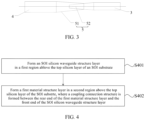
- FIG. 4 is a flow chart of a method for manufacturing a phased array LiDAR transmitting chip of multi-layer materials according to a sixth embodiment of the present disclosure. As shown in FIG. 4 , the method for manufacturing a phased array LiDAR transmitting chip of multi-layer materials provided in this embodiment includes the following steps.
- Step 401 form an SOI silicon waveguide structure layer 3 in a first region 30 above a top silicon layer of an SOI substrate.
- a waveguide pattern of the SOI silicon waveguide structure layer 3 may be transferred to the top silicon layer of the SOI substrate by using an electron beam exposure process or a stepper lithography process, and the SOI silicon waveguide structure layer 3 may be formed in the first region 30 by using an ICP etching process.
- Other processes may also be used to form the SOI silicon waveguide structure layer 3 in the first region 30 above the top silicon layer of the SOI substrate, which is not limited in this embodiment.
- first region 30 may be located at a rear end on the top silicon layer of the SOI substrate.
- Step 402 form a first material structure layer 4 in a second region 40 above the top silicon layer of the SOI substrate, where a coupling connection structure 5 is formed between the rear end of the first material structure layer 4 and the front end of the SOI silicon waveguide structure layer 3.
- the waveguide pattern of the first material structure layer 4 may be transferred to the first material structure layer 4 by using the electron beam exposure process or the stepper lithography process, and the first material structure layer 4 may be formed in the second region 40 by using the ICP etching process.
- Other processes may also be used to form the first material structure layer 4 in the second region 40 above the top silicon layer of the SOI substrate, which is not limited in this embodiment.
- the second region 40 may be located at the front end of the top silicon layer of the SOI substrate. And projection areas of the first region 30 and the second region 40 overlap each other to form the coupling connection structure 5.
- first region 30 may also be located at the front end on the top silicon of the SOI substrate, and accordingly, the second region 40 may be located at the rear end on the top silicon of the SOI substrate, and projection areas of the first region 30 and the second region 40 overlap each other to form the coupling connection structure 5.
- the first material structure layer 4 includes: an input coupler 41 and a beam splitter 42.
- a front waveguide pattern in the first material structure layer 4 forms the input coupler 41, and a rear waveguide pattern in the first material structure layer 4 forms the beam splitter 42.
- the input coupler 41 is configured to couple input light to a chip.
- the beam splitter 42 is configured to split the light wave coupled to the chip.
- the non-linear refractive index of the first material in the first material structure layer 4 is lower than the non-linear refractive index of a silicon material, and the first material is compatible with a CMOS process.
- the SOI silicon waveguide structure layer 3 and the first material structure layer 4 are formed, the SOI silicon waveguide structure layer 3 and the first material structure layer 4 are not on the same horizontal plane.
- the SOI silicon waveguide structure layer 3 may be either below the first material structure layer 4 or above the first material structure layer 4, so that a coupling connection structure 5 is formed between the rear end of the beam splitter 42 of the first material structure layer 4 and the front end of the SOI silicon waveguide structure layer 3.
- phased array LiDAR transmitting chip of multi-layer materials provided in this embodiment may be applied to manufacture the phased array LiDAR transmitting chip of multi-layer materials in the first embodiment of the present disclosure.
- the phased array LiDAR transmitting chip of multi-layer materials has the same structure and function as that in the first embodiment, and details will not be described here again.
- FIG. 5 is a flow chart of a method for manufacturing a phased array LiDAR transmitting chip of multi-layer materials according to a seventh embodiment of the present disclosure. As shown in FIG. 5 , the method for manufacturing a phased array LiDAR transmitting chip of multi-layer materials provided in this embodiment is based on the method provided in the sixth embodiment, and further refines the steps 401 and 402 and added some other steps. The method for manufacturing a phased array LiDAR transmitting chip of multi-layer materials according to this embodiment includes following steps.
- Step 501 form an SOI silicon waveguide structure layer 3 in a first region 30 above the top silicon layer of an SOI substrate.
- FIG. 6 is a structure diagram of an SOI substrate according to the seventh embodiment of the present disclosure.
- FIG. 7 is a structure diagram after step 501 of the method for manufacturing a phased array LiDAR transmitting chip of multi-layer materials according to the seventh embodiment of the present disclosure is executed. As shown in FIG. 7 , a first waveguide pattern is transferred to the top silicon layer of the SOI substrate by using an electron beam exposure process or a stepper lithography process and the SOI silicon waveguide structure layer 3 is formed in the first region 30 by using an ICP etching process.
- the first region 30 is a rear-end region located above the top silicon layer of the SOI substrate.
- Step 502 perform ion implantation in a phase modulation region of the SOI silicon waveguide structure layer 3 to form a PIN junction or a PN junction, for fabricating phase modulators 31.
- the first region 30 includes a phase modulation region, and the phase modulation region is located at the front end of the first region 30.
- Step 503 transfer a grating pattern to the top silicon layer of the SOI substrate by using an electron beam exposure process or a stepper lithography process, and form a grating 7 by using an ICP etching process to fabricate the optical antenna 32.
- FIG. 8 is a structure diagram after step 503 of the method for manufacturing a phased array LiDAR transmitting chip of multi-layer materials according to the seventh embodiment of the present disclosure is executed. As shown in FIG. 8 , the grating 7 is located at the rear end of the first region 30.
- the first waveguide pattern constitutes the waveguide pattern of the SOI silicon waveguide structure layer 3.
- a front end of the SOI silicon waveguide structure layer 3 is silicon waveguides 52 connected to the coupling connection structure 5.
- the silicon waveguides first pass through curved silicon waveguides to increase spacings between the silicon waveguides in the regions of the phase modulators 31, thus achieving thermal or electrical isolation, then pass through curved silicon waveguides to reach the waveguide region of the optical antenna 32 with the waveguide spacing reduced to 500 nm to 2.5 ⁇ m.
- Step 504 grow a second material layer 6 on the chip by using a PECVD process, where the refractive index of the second material layer 6 is lower than the refractive index of the first material structure layer 4 and the SOI silicon waveguide structure layer 3.
- FIG. 9 is a structure diagram after step 504 of the method for manufacturing a phased array LiDAR transmitting chip of multi-layer materials according to the seventh embodiment of the present disclosure is executed.
- the first material structure layer 4 and the SOI silicon waveguide structure layer 3 are separated by the second material layer 6, and the second material layer 6 is compatible with the CMOS process.
- the second material layer 6 may be a silicon dioxide layer.
- Step 505 grow a first material layer in a second region 40 above the second material layer 6 by using the PECVD process.
- FIG. 10 is a structure diagram of the method for manufacturing a phased array LiDAR transmitting chip of multi-layer materials according to the seventh embodiment of the present invention after executing step 506.
- the second region 40 is a front-end region above the second material layer 6.
- Step 507 grow an optical isolation layer 8 on the chip by using the PECVD process.
- a material of the optical isolation layer 8 may be a silicon dioxide material.
- Step 508 form, by using the ICP etching process, through holes on corresponding positions of thermodes and electrodes, the through holes leading to the SOI silicon waveguide structure layer 3.
- Step 509 grow a heating metal material and an electrode metal material by using a magnetron sputtering process or a thermal evaporation process, and form thermodes 10, metal leads 11 and electrodes 9 by using a lithography process.
- FIG. 12 is a structure diagram after step 509 of the method for manufacturing a phased array LiDAR transmitting chip of multi-layer materials according to the seventh embodiment of the present disclosure is executed.
- materials of the thermodes 10 and the metal leads 11 are not limited herein.
- the resistivity of the thermodes 10 may be one order of magnitude greater than the resistivity of the metal leads 11.
- Step 510 grow a protective layer 12 on the chip by using the PECVD process.
- the material of the protective layer 12 may be silicon dioxide.
- Step 511 form electrode windows 13 and a grating window 14 by using the ICP etching process.
- FIG. 13 is a structure diagram after step 511 of the method for manufacturing a phased array LiDAR transmitting chip of multi-layer materials according to the seventh embodiment of the present disclosure is executed.
- the protective layer 12 covers the entire chip, the electrode window 13 is located above the electrode, and the grating window 14 is located above the grating.
- phased array LiDAR transmitting chip of multi-layer materials provided in this embodiment may be applied to manufacture the phased array LiDAR transmitting chip of multi-layer materials in the fourth embodiment of the present disclosure, where the structure and function of the phased array LiDAR transmitting chip of multi-layer materials in this embodiment are the same as those of the fourth embodiment, and thus will not be described here again.
Landscapes
- Physics & Mathematics (AREA)
- Engineering & Computer Science (AREA)
- General Physics & Mathematics (AREA)
- Computer Networks & Wireless Communication (AREA)
- Radar, Positioning & Navigation (AREA)
- Remote Sensing (AREA)
- Nonlinear Science (AREA)
- Optics & Photonics (AREA)
- Optical Modulation, Optical Deflection, Nonlinear Optics, Optical Demodulation, Optical Logic Elements (AREA)
- Optical Integrated Circuits (AREA)
Description
- The present disclosure relates to the field of light detection and ranging (LiDAR) technologies and, in particular, to a phased array LiDAR transmitting chip of multi-layer materials, a manufacturing method thereof, and a LiDAR device.
- The concept of phased array LiDAR has been proposed for a long time, and various design schemes are also being developed. Current phased array LiDAR chips use silicon on insulator (SOI) material as a substrate, and make use of the characteristics of silicon to fabricate various on-chip structures, thus realizing basic functions of LiDAR.
- But silicon has its own shortcomings. Since silicon is a strongly nonlinear material with a strong two-photon absorption effect and a free carrier absorption effect, and its low-order nonlinear refractive index is very large, making it difficult to transmit high-power light in a silicon waveguide with low loss, which greatly limits the optical power input to the phased array LiDAR transmitting chip, and seriously affects the detection performance of the LiDAR and brings great pressure to the signal detection part.
- CHUNG SUNGWON ET AL: "A Monolithically Integrated Large-Scale Optical Phased Array in Silicon-on-Insulator CMOS", IEEE JOURNAL OF SOLID-STATE CIRCUITS, IEEE, USA, vol. 53, no. 1, 18 October 2017 (2017-10-18), pages 275 - 296, discloses that a large-scale monolithic silicon nanophotonic phased array on a chip creates and dynamically steers a high-resolution optical beam in free space, enabling emerging applications in sensing, imaging, and communication. The scalable architecture leverages sub-array structure, mitigating the impact of process variation on the phased array performance. In addition, sharing control electronics among multiple optical modulators in the scalable architecture reduces the number of digital-to-analog converters (DACs) required for an N 2 array from O(N 2) to O(N), allowing a small silicon footprint. An optical phased array for 1550-nm wavelength with 1024 uniformly spaced optical grating antennas, 1192 optical variable phase shifters, and 168 optical variable attenuators is integrated into a 5.7 mm × 6.4 mm chip in a commercial 180-nm silicon-on-insulator RF CMOS technology. The control signals for the optical variable phase shifters and attenuators are provided by 136 DACs with 14-bit nonuniform resolution using 2.5-V input-output transistors. The implemented phased array can create 0.03° narrow optical beams that can be steered unambiguously within ±22.5°.
- NOTAROS JELENA ET AL: "CMOS-Compatible Optical Phased Arrays with Monolithically-Integrated Erbium Lasers", 2018 CONFERENCE ON LASERS AND ELECTRO-OPTICS (CLEO), OSA, 13 May 2018 (2018-05-13), pages 1 - 2, discloses that an electronically-steerable integrated optical phased array powered by an on-chip erbium-doped laser is experimentally demonstrated. This system represents the first demonstration of a rare-earth-doped laser monolithically integrated with an active CMOS-compatible silicon photonics system.
- Embodiments of the present disclosure provides a phased array LiDAR transmitting chip of multi-layer materials, a manufacturing method thereof, and a LiDAR device, solving the power limit problem of a phased array LiDAR chip in the prior art, so that the optical power input into the phased array LiDAR transmitting chip may be greatly increased, thus greatly improving the detection performance of LiDAR, and reducing a great deal of pressure on the signal detection part. The invention is set out in the appended set of claims.
- In a first aspect, an embodiment of the present disclosure provides a phased array LiDAR transmitting chip of multi-layer materials, including: a first material structure layer, an SOI silicon waveguide structure layer, and a coupling connection structure, the first material structure layer including: an input coupler and a beam splitter;
- the input coupler is optically connected to the beam splitter; and the beam splitter is optically connected to the SOI silicon waveguide structure layer through the coupling connection structure;
- the input coupler is configured to couple input light to the chip;
- the beam splitter is configured to split a light wave coupled to the chip;
- the coupling connection structure is configured to couple each of the split light waves into a corresponding silicon waveguide in the SOI silicon waveguide structure layer;
- where the non-linear refractive index of a first material in the first material structure layer is lower than the non-linear refractive index of a silicon material and the first material is compatible with a CMOS process.
- Further, in an implementation of the phased array LiDAR transmitting chip of multi-layer materials described above, the SOI silicon waveguide structure layer includes: phase modulators and an optical antenna;
- the phase modulators and the optical antenna are connected through silicon waveguides;
- the phase modulators are configured to change the phase of a light wave coupled to a corresponding silicon waveguide in the SOI silicon waveguide structure layer; and
- the optical antenna is configured to transmit phase-changed light waves in silicon waveguides into space.
- Further, in an implementation of the phased array LiDAR transmitting chip of multi-layer materials described above, the first material structure layer is located above the SOI silicon waveguide structure layer, and the first material structure layer and the SOI silicon waveguide structure layer are separated by a second material layer;
where the refractive index of the second material layer is lower than the refractive index of the first material structure layer and the SOI silicon waveguide structure layer. - Further, in an implementation of the phased array LiDAR transmitting chip of multi-layer materials described above, the coupling connection structure includes first material coupling waveguides and silicon coupling waveguides;
- the first material coupling waveguides are connected to the rear end of a first material waveguide of the beam splitter, and the silicon coupling waveguides are connected to the front end of a silicon waveguide in the SOI silicon waveguide structure layer;
- the first material coupling waveguides and the silicon coupling waveguides have respective wedge structures, the first material coupling waveguides and the silicon coupling waveguides have their tips facing each other, and the first material coupling waveguides and the silicon coupling waveguides have their projection areas overlap each other.
- Further, in an implementation of the phased array LiDAR transmitting chip of multi-layer materials described above, the first material coupling waveguides and the silicon coupling waveguides have a tip width of 100 nm to 300 nm;
- the rear-end width of each of the first material coupling waveguides is the same as the width of a corresponding first material waveguide of the beam splitter, and the rear-end width of the silicon coupling waveguides is the same as the width of a silicon waveguide in the SOI silicon waveguide structure layer; and
- an overlapping region has a length of 10 µm to 100 µm.
- Further, in an implementation of the phased array LiDAR transmitting chip of multi-layer materials described above, the first material structure layer further includes a first material backbone waveguide;
the input coupler is optically connected to the beam splitter through the first material backbone waveguide. - In a second aspect, an embodiment of the present disclosure provides a phased array LiDAR device, including the phased array LiDAR transmitting chip of multi-layer materials according to any implementation of the first aspect described above.
- In a third aspect, an embodiment of the present disclosure provides a method for manufacturing the phased array LiDAR transmitting chip of multi-layer materials according to any implementation of the first aspect described above, the method including:
- forming an SOI silicon waveguide structure layer in a first region above the top silicon layer of an SOI substrate; and
- forming a first material structure layer in a second region above the top silicon layer of the SOI substrate, so as to form a coupling connection structure between the rear end of the first material structure layer and the front end of the SOI silicon waveguide structure layer;
- where the first material structure layer includes: an input coupler and a beam splitter; the non-linear refractive index of a first material in the first material structure layer is lower than the non-linear refractive index of a silicon material and the first material is compatible with a CMOS process.
- Further, in an implementation of the method described above, the forming an SOI silicon waveguide structure layer in a first region above a top silicon layer of an SOI substrate includes:
transferring a first waveguide pattern to the top silicon layer of the SOI substrate by using an electron beam exposure process or a stepper lithography process, and forming the SOI silicon waveguide structure layer in the first region by using an inductively coupled plasma (ICP) etching process. - Further, in an implementation of the method described above, after the forming the SOI silicon waveguide structure layer in the first region above the top silicon layer of the SOI substrate, further includes:
- performing ion implantation in the phase modulation region of the SOI silicon waveguide structure layer to form a PIN junction or a PN junction, for fabricating phase modulators;
- transferring a grating pattern to the top silicon layer of the SOI substrate by using the electron beam exposure process or the stepper lithography process, and forming a grating by using the ICP etching process to fabricate the optical antenna; and
- growing a second material layer on the chip by using a plasma enhanced chemical vapor deposition (PECVD) process, where the refractive index of the second material layer is lower than the refractive index of the first material structure layer and the SOI silicon waveguide structure layer.
- Further, in an implementation of the method described above, the forming a first material structure layer in a second region above the top silicon layer of the SOI substrate, includes:
- growing a first material layer in the second region above the second material layer by using the PECVD process;
- transferring a second waveguide pattern to the first material layer by using the electron beam exposure process or the stepper lithography process, and fabricating the first material structure layer in the second region by using the ICP etching process
- Further, in an implementation of the method described above, after forming a first material structure layer in a second region above the top silicon layer of the SOI substrate, the method further includes:
- growing an optical isolation layer on the chip by using the PECVD process;
- forming through holes on corresponding positions of thermodes and electrodes by using the ICP etching process, the thorough holes leading to the SOI silicon waveguide structure layer;
- growing a heating metal material and an electrode metal material by using a magnetron sputtering process or a thermal evaporation process, and forming thermodes, metal leads and electrodes by using a lithography process;
- growing a protective layer on the chip by using the PECVD process; and
- forming electrode windows and a grating window by using the ICP etching process.
- Embodiments of the present disclosure provide a phased array LiDAR transmitting chip of multi-layer materials, a manufacturing method thereof, and a LiDAR device. The phased array LiDAR transmitting chip of multi-layer materials includes: a first material structure layer, a SOI silicon waveguide structure layer, and a coupling connection structure. The first material structure layer includes an input coupler and a beam splitter; the input coupler is optically connected to the beam splitter; the beam splitter is optically connected to the SOI silicon waveguide structure layer through the coupling connection structure; the input coupler is configured to couple input light into the chip; the beam splitter is configured to split a light wave coupled into the chip; the coupling connection structure is configured to couple each of the split light waves into a silicon waveguide corresponding to the SOI silicon waveguide structure layer; where the non-linear refractive index of the first material in the first material structure layer is lower than the non-linear refractive index of a silicon material, and the first material is compatible with a CMOS process. Because the non-linear refractive index of the first material in the first material structure layer is lower than the non-linear refractive index of the silicon material, the input coupler in the first material structure layer may couple a high-power light wave to the chip, and then divide the light wave into several light waves through the beam splitter, so as to reduce the optical power in each of first material waveguides, and enable the optical power in each of the first material waveguides to satisfy normal transmission in the silicon waveguide. As a result, the optical power input into the phased array LiDAR transmitting chip of multi-layer materials may be greatly increased, thus greatly improving the detection performance of LiDAR, and reducing a lot of pressure on the signal detection part.
- It should be understood that what is described in the summary above is not intended to limit key features or important features of the embodiments of the present disclosure, nor is it intended to limit the scope of the present disclosure. Other features of the present disclosure will be easily understood from the following description.
- In order to make the technical solutions in embodiments of the present disclosure or in the prior art clearer, the accompanying drawings used in the description of embodiments of the present disclosure or the prior art are briefly described hereunder. Obviously, the described drawings are merely some embodiments of present disclosure. For persons of ordinary skill in the art, other drawings may be obtained based on these drawings without any creative efforts.
-
FIG. 1 is a structure diagram of a phased array LiDAR transmitting chip of multi-layer materials according to a first embodiment of the present disclosure. -
FIG.2 is a structure diagram of a phased array LiDAR transmitting chip of multi-layer materials according to a second embodiment of the present disclosure. -
FIG. 3 is a structure diagram of a coupling connection structure of a phased array LiDAR transmitting chip of multi-layer materials according to a third embodiment of the present disclosure. -
FIG. 4 is a flow diagram of a method for manufacturing a phased array LiDAR transmitting chip of multi-layer materials according to a sixth embodiment of the present disclosure. -
FIG. 5 is a flow diagram of a method for manufacturing a phased array LiDAR transmitting chip of multi-layer materials according to a seventh embodiment of the present disclosure. -
FIG. 6 is a structure diagram of an SOI substrate according to the seventh embodiment of the present disclosure. -
FIG. 7 is a structure diagram afterstep 501 of the method for manufacturing a phased array LiDAR transmitting chip of multi-layer materials according to the seventh embodiment of the present disclosure is executed. -
FIG. 8 is a structure diagram afterstep 503 of the method for manufacturing a phased array LiDAR transmitting chip of multi-layer materials according to the seventh embodiment of the present disclosure is executed. -
FIG. 9 is a structure diagram afterstep 504 of the method for manufacturing a phased array LiDAR transmitting chip of multi-layer materials according to the seventh embodiment of the present disclosure is executed. -
FIG. 10 is a structure diagram afterstep 506 of the method for manufacturing a phased array LiDAR transmitting chip of multi-layer materials according to the seventh embodiment of the present disclosure is executed. -
FIG. 11 is a structure diagram afterstep 507 of the method for manufacturing a phased array LiDAR transmitting chip of multi-layer materials according to the seventh embodiment of the present disclosure is executed. -
FIG. 12 is a structure diagram afterstep 509 of the method for manufacturing a phased array LiDAR transmitting chip of multi-layer materials according to the seventh embodiment of the present disclosure is executed. -
FIG. 13 is a structure diagram of the method after step 511 for manufacturing a phased array LiDAR transmitting chip of multi-layer materials according to the seventh embodiment of the present disclosure is executed. -
- 1
- Substrate silicon layer
- 2
- Buried oxide layer
- 21
- Top silicon layer
- 3
- SOI Silicon waveguide structure layer
- 30
- First region
- 31
- Phase modulator
- 32
- Optical antenna
- 4
- First material structure layer
- 40
- Second region
- 41
- Input coupler
- 42
- Beam splitter
- 5
- Coupling connection structure
- 51
- First material coupling waveguide
- 52
- Silicon coupling waveguide
- 6
- Second material layer
- 7
- Grating
- 8
- Optical isolation layer
- 9
- Electrode
- 10
- Thermode
- 11
- Metal lead
- 12
- Protective layer
- 13
- Electrode window
- 14
- Grating window
- Embodiments of the present disclosure will be described in further details in the following with reference to the accompanying drawings. Although some embodiments of the present disclosure are shown in the drawings, it should be understood that the present disclosure may be implemented in various forms and should not be construed as being limited to the embodiments described below. Rather, these embodiments are provided for a more thorough and complete understanding of the present disclosure. It should be understood that the drawings and embodiments of the present disclosure are only for exemplary purposes, and are not intended to limit the protection scope of the present disclosure.
- The terms "first", "second", "third", "fourth", and the like (if any) in the description and claims of the embodiments of the present disclosure and the above-mentioned drawings are used to distinguish similar objects, and it does not set a specific order or sequence. It should be understood that the data used in this way are interchangeable under appropriate circumstances, so that the embodiments described herein may be implemented out of the order illustrated or described herein. In addition, the terms "including" and "having" and any of their variations are intended to cover non-exclusive inclusion.
-
FIG. 1 is a structure diagram of a phased array LiDAR transmitting chip of multi-layer materials according to a first embodiment of the present disclosure. As shown inFIG. 1 , the phased array LiDAR transmitting chip of multi-layer materials provided in this embodiment includes: a firstmaterial structure layer 4, an SOI siliconwaveguide structure layer 3, and acoupling connection structure 5, and the firstmaterial structure layer 4 includes aninput coupler 41 and abeam splitter 42. - The
input coupler 41 is optically connected to thebeam splitter 42; thebeam splitter 42 is optically connected to the SOI siliconwaveguide structure layer 3 through thecoupling connection structure 5. - The
input coupler 41 is configured to couple input light to the chip. Thebeam splitter 42 is configured to split a light wave coupled to the chip. Thecoupling connection structure 5 is configured to couple each of the split light waves to a corresponding silicon waveguide in the SOI siliconwaveguide structure layer 3. - The non-linear refractive index of a first material in the first
material structure layer 4 is lower than the non-linear refractive index of a silicon material, and the first material is compatible with a complementary metal oxide semiconductor (CMOS) process. - The term "non-linear refractive index" refers to low-order non-linear refractive indexes. The low-order non-linear refractive indexes may also be the first-order non-linear refractive index, the second-order non-linear refractive index, the third-order non-linear refractive index, etc.
- Specifically, in this embodiment, the phased array LiDAR transmitting chip of multi-layer materials is integrated on an SOI substrate satisfying the CMOS process. The SOI substrate includes a
substrate silicon layer 1, a buriedoxide layer 2 and atop silicon layer 21 from bottom to top. The material and thickness of each layer of the SOI substrate are not limited in this embodiment. For example, the material and thickness of each layer may be customized according to different needs, or a conventional standard CMOS process SOI substrate product may be used. For example, the material of thesubstrate silicon layer 1 is silicon with a thickness of 500 µm to 600 µm. The material of the buriedoxide layer 2 is silicon dioxide with a thickness of 2 µm, and the material of thetop silicon layer 21 is silicon with a thickness of 220 nm or 340 nm. - For the convenience of description, the following embodiments will use the above-mentioned standard CMOS process SOI substrate to integrate the phased array LiDAR transmitting chip of multi-layer materials according to the embodiments of the present disclosure, where the thickness of the
top silicon layer 21 nm is 220 nm. - Because silicon has a large low-order non-linear refractive index, and the silicon material exhibits a strong two-photon absorption effect and free carrier absorption effect, so generally the optical power allowed to be transmitted in silicon waveguides is very small, usually about 100 mw. This makes a conventional pure silicon-based phased array LiDAR transmitting chip unable to achieve on-chip processing and emission of high-power lasers, which seriously reduces the detection performance of the LiDAR.
- In order to solve the above problems, in this embodiment, the first
material structure layer 4 having a lower nonlinear refractive index than the nonlinear refractive index of a silicon material is used. The firstmaterial structure layer 4 includes multiple forms of first material waveguides therein to form theinput coupler 41 and thebeam splitter 42. Moreover, the first material in the firstmaterial structure layer 4 is compatible with the CMOS process. The first material may be a silicon-like material, such as silicon nitride or silicon oxynitride. Therefore, theinput coupler 41 in the firstmaterial structure layer 4 is configured to couple light waves to the chip and may couple high-power input light to the firstmaterial structure layer 4. - Because the first material has a relatively low refractive index, then the size of the
input coupler 41 of the first material is enabled to be larger than the size of a silicon input coupler in the prior art. Therefore, the mismatch between the spot size of theinput coupler 41 and the fiber spot size may be greatly reduced, and the coupling efficiency may be effectively improved. Theinput coupler 41 of the first material may achieve a higher coupling efficiency than the silicon input coupler in the prior art. Moreover, the first material is not easily affected by two-photon absorption effect and carrier absorption effect, and its first order nonlinear refractive index is nearly 20 times smaller than the first order nonlinear refractive index of silicon, enabling light waves of optical power that is much higher than optical power transmitted in the silicon waveguide to be transmitted in the waveguide of the firstmaterial structure layer 4. - In this embodiment, the
beam splitter 42 is configured to split a light wave coupled to the chip, the light wave coupled to theinput coupler 41, after passing through thebeam splitter 42, is divided into several light waves so that the optical power in each of the first material waveguides after beam-splitting by thebeam splitter 42 is much smaller. After the light wave is divided into a sufficient number of light waves, optical power of each of the light waves may satisfy that after being normally transmitted in the silicon waveguide, then each of the light waves is coupled to the a corresponding silicon waveguide in the SOIsilicon waveguide structure 3 through thecoupling connection structure 5. - The phased array LiDAR transmitting chip of multi-layer materials provided in this embodiment includes: a first
material structure layer 4, an SOI siliconwaveguide structure layer 3, and acoupling connection structure 5, and the firstmaterial structure layer 4 includes aninput coupler 41 and abeam splitter 42; theinput coupler 41 is optically connected to thebeam splitter 42; thebeam splitter 42 is optically connected to the SOI siliconwaveguide structure layer 3 through thecoupling connection structure 5; theinput coupler 41 is configured to couple input light to the chip; thebeam splitter 42 is configured to split the light wave coupled to the chip; thecoupling connection structure 5 is configured to couple each of the split light waves to a corresponding silicon waveguide in the SOI siliconwaveguide structure layer 3; where the non-linear refractive index of a first material in the firstmaterial structure layer 4 is lower than the non-linear refractive index of a silicon material and the first material is compatible with a CMOS process. Because the non-linear refractive index of the first material in the firstmaterial structure layer 4 is lower than the non-linear refractive index of the silicon material, theinput coupler 41 in the firstmaterial structure layer 4 may couple a high-power light wave into the chip, and then divide the light wave into several light waves through thebeam splitter 42, so as to reduce the optical power in each of the first material waveguides and enable the optical power in each of the first material waveguides to be able to satisfy normal transmission in the silicon waveguide. As a result, the optical power input into the phased array LiDAR transmitting chip of multi-layer materials may be greatly increased, thus greatly improving the detection performance of LiDAR, and reducing a lot of pressure on the signal detection part. - Further, as shown in
FIG. 1 , in the phased array LiDAR transmitting chip of multi-layer materials provided in this embodiment, the SOI siliconwaveguide structure layer 3 includes:phase modulators 31 and anoptical antenna 32. - The
phase modulators 31 and theoptical antenna 32 are connected through silicon waveguides. - Specifically, the
phase modulators 31 are configured to change the phase of a light wave coupled to a corresponding silicon waveguide in the SOI siliconwaveguide structure layer 3. Theoptical antenna 32 is configured to transmit phase-changed light waves in the silicon waveguides into space. - In this embodiment, the
phase modulators 31 and theoptical antenna 32 are optically connected through silicon waveguides. Thephase modulators 31 forms an electrode with a silicon waveguide and adjusts the refractive index of the silicon waveguide by applying current or voltage bias, thus changing the phase of the light wave in each waveguide. The light waves in the silicon waveguides are phase-adjusted by thephase modulators 31 and then transmitted by the silicon waveguides to theoptical antenna 32 and emitted into space. - In the phased array LiDAR transmitting chip of multi-layer materials provided in this embodiment, the SOI silicon
waveguide structure layer 3 includesphase modulators 31 and anoptical antenna 32. The phase modulators and the optical antenna are connected through the silicon waveguides; thephase modulators 31 are configured to change the phase of a light wave coupled to a corresponding silicon waveguide in the SOI siliconwaveguide structure layer 3. Theoptical antenna 32 is configured to transmit phase-changed light waves in the silicon waveguides into space. Therefore, the input high-power light to the phased array LiDAR transmitting chip of multi-layer material s may be emit into space, thus greatly improving the detection performance of LiDAR and reducing a lot of pressure on signal detection part. -
FIG. 2 is a structure diagram of a phased array LiDAR transmitting chip of multi-layer materials according to a second embodiment of the present disclosure. As shown inFIG. 2 , the phased array LiDAR transmitting chip provided in this embodiment is based on the phased array LiDAR transmitting chip of multi-layer materials in the first embodiment of present disclosure, and further includes: asecond material layer 6. - Further, in this embodiment, the first
material structure layer 4 is located above the SOI siliconwaveguide structure layer 3. And the firstmaterial structure layer 4 and the SOI siliconwaveguide structure layer 3 are separated by thesecond material layer 6. - The refractive index of the
second material layer 6 is lower than the refractive index of the firstmaterial structure layer 4 and the SOI siliconwaveguide structure layer 3. - Specifically, in this embodiment, the first
material structure layer 4 and the SOI siliconwaveguide structure layer 3 are separated by thesecond material layer 6 having the lower refractive index than both the firstmaterial structure layer 4 and the SOI siliconwaveguide structure layer 3. Thesecond material layer 6 may be compatible with a CMOS process. For example, thesecond material layer 6 may be a silicon dioxide layer. In this embodiment, the thickness of thesecond material layer 6 corresponds to an operating wavelength of the phased array LiDAR transmitting chip. The thickness is approximately the quotient of a quarter of the operating wavelength and the refractive index of the second material. If the operating wavelength of the phased array laser transmitting chip is 1.5 µm to 1.6 µm, then the thickness of thesecond material layer 6 may be set as 50 nm to 500 nm. -
FIG. 3 is a structure diagram of acoupling connection structure 5 of a phased array LiDAR transmitting chip of multi-layer materials according to a third embodiment of the present disclosure, which is a top view ofFIG. 2 along the direction A. With reference toFIG. 1 andFIG. 3 , in this embodiment, the firstmaterial coupling waveguide 51 is connected to the rear end of a corresponding first material waveguide of thebeam splitter 42, and thesilicon coupling waveguide 52 is connected to the front end of a corresponding silicon waveguide of the SOI siliconwaveguide structure layer 3. - The first
material coupling waveguide 51 and thesilicon coupling waveguide 52 have respective wedge structures, the firstmaterial coupling waveguide 51 and thesilicon coupling waveguide 52 have their tips facing each other, and the firstmaterial coupling waveguide 51 and thesilicon coupling waveguide 52 have their projection areas overlap each other. - In a practical application, the
coupling connection structure 5 is wedge structures overlapping with each other, and there is asecond material layer 6 between the firstmaterial coupling waveguides 51 and thesilicon coupling waveguides 52, and two wedge structures have their tips facing each other. In the firstmaterial coupling waveguides 51 and thesilicon coupling waveguides 52, the wedge structures are used to reduce restriction on light waves in the waveguides, so that the light waves are coupled from the firstmaterial coupling waveguides 51 to thesilicon coupling waveguides 52 through the principle of evanescent wave coupling. - The tip width of the first
material coupling waveguide 51 and the tip width of thesilicon coupling waveguide 52 may be determined by a fabrication process and processing accuracy. In some implementations, the firstmaterial coupling waveguide 51 and thesilicon coupling waveguide 52 have a tip width of 100 nm to 300 nm. - In some implementations, the front-end width of the first
material coupling waveguide 51 is identical to the width of a corresponding first material waveguide of thebeam splitter 42, and the rear-end width of thesilicon coupling waveguide 52 is identical to the width of a corresponding silicon waveguide in the SOI siliconwaveguide structure layer 3. That is, the rear-end widths of the firstmaterial coupling waveguide 51 and thesilicon coupling waveguide 52 are identical to the widths of the waveguides connected thereto, respectively. - In some implementations, first material waveguides of the
beam splitter 42 have a width of 800 nm to 1 µm, and then the firstmaterial coupling waveguides 51 have a front-end width of 800 nm to 1 µm. Silicon waveguides in the SOI siliconwaveguide structure layer 3 have a width of 400 nm to 500 nm, and then thesilicon coupling waveguides 52 have a rear-end width of 400 nm to 500 nm. - In some implementations, an overlapping region has a length of 10 µm to 100 µm. That is, an overlapping region in projection areas of the first
material coupling waveguide 51 and thesilicon coupling waveguide 52 has a length of 10 µm to 100 µm. - In the phased array LiDAR transmitting chip of multi-layer materials provided in this embodiment, the
coupling connection structure 5 includes firstmaterial coupling waveguides 51 andsilicon coupling waveguides 52; the firstmaterial coupling waveguides 51 are connected to the rear end of a corresponding first material waveguide of thebeam splitter 42, and thesilicon coupling waveguides 52 are connected to the front end of a corresponding silicon waveguide in the SOI siliconwaveguide structure layer 3; and the firstmaterial coupling waveguides 51 and thesilicon coupling waveguides 52 have respective wedge structures, the firstmaterial coupling waveguide 51 and thesilicon coupling waveguide 52 have their tips facing each other, and the firstmaterial coupling waveguides 51 and thesilicon coupling waveguides 52 have their projection areas overlapping each other. Moreover, the tip widths, the rear-end widths, and the length of the overlapping region of the firstmaterial coupling waveguides 51 and thesilicon coupling waveguides 52 are set to corresponding preset ranges, which may effectively couple a light wave from the first material waveguide to the silicon waveguide and achieve an coupling spectral ratio of 0-100%. - This embodiment further refines the first material structure layer and the SOI silicon waveguide structure layer on the basis of the phased array LiDAR transmitting chip of multi-layer materials provided in the third embodiment of the present disclosure. The phased array LiDAR transmitting chip of multi-layer materials provided in this embodiment further includes the following solutions.
- Further, in this embodiment, the first material structure layer further includes a first material backbone waveguide.
- The
input coupler 41 is optically connected to thebeam splitter 42 through the first material backbone waveguide. - Preferably, each waveguide in the phased array LiDAR transmitting chip of multi-layer materials is a single-mode waveguide in TE mode.
- Specifically, in this embodiment, waveguides in the first material structure layer, waveguides in the SOI silicon waveguide structure layer, and waveguides in the coupling connection structure are all single-mode waveguides in TE mode.
- Further, in this embodiment, the
input coupler 41 is an end-face coupler or a grating coupler. Thebeam splitter 42 is a cascaded multimode interference coupler, a star coupler or a directional coupler. - Specifically, in this embodiment, the end-face coupler or the grating coupler may be selected to couple a light wave to the chip, then the light wave is transmitted by the single-mode waveguide in the TE mode to the first material waveguide of the
beam splitter 42 which may be any one of the multimode interference coupler, the star coupler or the directional coupler. When the light wave is divided into a sufficient number of light waves, and each of the optical power satisfies normal transmission in the silicon waveguide, the light waves may be coupled from a first material waveguide to a silicon waveguide in the SOI siliconwaveguide structure layer 3 through thecoupling connection structure 5. - Further, in this embodiment, the
phase modulators 31 are electro-optic phase modulators or thermo-optic phase modulators. - Specifically, in this embodiment, the
phase modulator 31 is an electro-optic phase modulator or a thermo-optic phase modulator. The structure of the electro-optic phase modulator is formed as follows: ion implantation is performed on silicon flat plates on both sides of a silicon waveguide in the SOI siliconwaveguide structure layer 3 to form a PIN junction or a PN junction with the silicon waveguide; and when a current is passed, the refractive index of a silicon material may be adjusted by the current, thus changing the phase of a light wave in each silicon waveguide. The thermo-optic phase modulator may be a top heating type or a two-side heating type, that is, the heating electrode is located on the top or both sides of the silicon waveguide, biased by the current or voltage. The heat generated by the heating electrode will be transferred to the silicon waveguide. Since silicon is a material with a high thermo-optic coefficient, it is easy to change the refractive index in the waveguide, thus changing the phase of the light wave in each waveguide. It should be noted that, while the heating electrode is too close to the waveguide, the heating electrode will absorb the light wave in the waveguide and cause a large loss, thus the heating electrode needs to be a certain distance away from the waveguide to avoid the loss, and the distance is generally greater than 2 µm. The materials of the heating electrode and metal lead are not limited in the embodiment, but generally the resistivity of the heating electrode is larger than the metal lead by around an order of magnitude. - In the phased array LiDAR transmitting chip of multi-layer materials provided in this embodiment, the
input coupler 41 is an end-face coupler or a grating coupler; thebeam splitter 42 is a cascaded multimode interference coupler, a star coupler or a directional coupler; and thephase modulators 31 are electro-optic phase modulators or thermo-optic phase modulators, enabling the phased array LiDAR transmitting chip of multi-layer materials to present various types and meet various requirements of different devices. - Further, in this embodiment, the
optical antenna 32 is a grating-type optical antenna array. - Specifically, in this embodiment, the light wave in each silicon waveguide is phase-adjusted by the
phase modulator 31 and transmitted by the silicon waveguide to theoptical antenna 32, and emitted into space by theoptical antenna 32. In this embodiment, theoptical antenna 32 is a second-order diffraction grating formed on a silicon waveguide array, that is, a grating-typeoptical antenna array 32. Specific parameters of the grating, such as grating period, duty cycle, and etching depth, are all related to the operating wavelength. When performing grating etching on a silicon waveguide, the grating period needs to be calculated first according to the etching depth. In order to obtain a small far-field divergence angle along the direction of the silicon waveguide and a high longitudinal LiDAR scanning resolution, the etching depth of the second-order diffraction grating of theoptical antenna 32 should be designed to be shallow, 20 nm to 100 nm. Because the light wavelength band is 1.5 µm to 1.6 µm, the effective refractive index of the silicon waveguide array for this band is about 2.38. According to the formula of the second-order diffraction grating, it is found that the period of the second-order diffraction grating is 600 nm to 680 nm, that is, the grating is formed on the silicon waveguide uniformly at a distance of the grating period. The width of the grating is determined by a duty cycle, that is, a ratio of the grating width to the grating period. It may be known from calculation that when the light wavelength band is 1.5 µm to 1.6 µm and the duty ratio of the second-order diffraction grating is 0.4 to 0.6, the external radiation efficiency may reach the highest. - Because the waveguide pitch of the
optical antenna 32 determines the maximum scanning angle of the final phased array LiDAR transmitting chip, so in this embodiment, the silicon waveguide pitch of theoptical antenna 32 is 500 nm to 2.5 µm. Theoptical antenna 32 will not limit the distribution form of the silicon waveguide. The distribution form may be a uniform distribution, or a gaussian distribution, a sinusoidal distribution, or other distribution forms. - Further, in this embodiment, the phased array LiDAR transmitting chip of multi-layer materials may further includes a protective layer.
- Specifically, the protective layer may cover the entire phased array LiDAR transmitting chip of multi-layer materials. The
protective layer 12 is a low refractive index protective layer. The material of the low-refractive-indexprotective layer 12 may be silicon dioxide, and the thickness may be 2 µm to 5 µm. - Further, in this embodiment, after the electrodes of the phased array LiDAR transmitting chip of multi-layer materials are set, windows are formed above the electrodes and the grating of the optical antenna for power input and light input and output. The windows above the grating of the
optical antenna 32 may be formed approximately 2 µm away from the grating. - The fifth embodiment of the present disclosure provides a phased array LiDAR. The phased array LiDAR includes the phased array LiDAR transmitting chip of multi-layer materials according to any one of the first to fourth embodiments of the present disclosure.
- The structure and function of the phased array LiDAR transmitting chip of multi-layer materials of the phased array LiDAR in this embodiment are similar to those of the phased array LiDAR transmitting chip of multi-layer materials in any one of the first to fourth embodiments of the present disclosure, which will not be described here again.
- In this embodiment, a light source may be made by coupling a laser outside the chip to a phased array LiDAR transmitting chip of multi-layer materials, or a laser bonded to the chip. The detector of the phased array LiDAR may be either an off-chip detector or a detector integrated on the chip, which is not limited in this embodiment.
-
FIG. 4 is a flow chart of a method for manufacturing a phased array LiDAR transmitting chip of multi-layer materials according to a sixth embodiment of the present disclosure. As shown inFIG. 4 , the method for manufacturing a phased array LiDAR transmitting chip of multi-layer materials provided in this embodiment includes the following steps. - Step 401: form an SOI silicon
waveguide structure layer 3 in afirst region 30 above a top silicon layer of an SOI substrate. - Specifically, in this embodiment, a waveguide pattern of the SOI silicon
waveguide structure layer 3 may be transferred to the top silicon layer of the SOI substrate by using an electron beam exposure process or a stepper lithography process, and the SOI siliconwaveguide structure layer 3 may be formed in thefirst region 30 by using an ICP etching process. Other processes may also be used to form the SOI siliconwaveguide structure layer 3 in thefirst region 30 above the top silicon layer of the SOI substrate, which is not limited in this embodiment. - Where the
first region 30 may be located at a rear end on the top silicon layer of the SOI substrate. - Step 402: form a first
material structure layer 4 in asecond region 40 above the top silicon layer of the SOI substrate, where acoupling connection structure 5 is formed between the rear end of the firstmaterial structure layer 4 and the front end of the SOI siliconwaveguide structure layer 3. - Specifically, in this embodiment, the waveguide pattern of the first
material structure layer 4 may be transferred to the firstmaterial structure layer 4 by using the electron beam exposure process or the stepper lithography process, and the firstmaterial structure layer 4 may be formed in thesecond region 40 by using the ICP etching process. Other processes may also be used to form the firstmaterial structure layer 4 in thesecond region 40 above the top silicon layer of the SOI substrate, which is not limited in this embodiment. - Where the
second region 40 may be located at the front end of the top silicon layer of the SOI substrate. And projection areas of thefirst region 30 and thesecond region 40 overlap each other to form thecoupling connection structure 5. - It should be understood that the
first region 30 may also be located at the front end on the top silicon of the SOI substrate, and accordingly, thesecond region 40 may be located at the rear end on the top silicon of the SOI substrate, and projection areas of thefirst region 30 and thesecond region 40 overlap each other to form thecoupling connection structure 5. - In this embodiment, the first
material structure layer 4 includes: aninput coupler 41 and abeam splitter 42. A front waveguide pattern in the firstmaterial structure layer 4 forms theinput coupler 41, and a rear waveguide pattern in the firstmaterial structure layer 4 forms thebeam splitter 42. Theinput coupler 41 is configured to couple input light to a chip. Thebeam splitter 42 is configured to split the light wave coupled to the chip. - The non-linear refractive index of the first material in the first
material structure layer 4 is lower than the non-linear refractive index of a silicon material, and the first material is compatible with a CMOS process. - In this embodiment, when the SOI silicon
waveguide structure layer 3 and the firstmaterial structure layer 4 are formed, the SOI siliconwaveguide structure layer 3 and the firstmaterial structure layer 4 are not on the same horizontal plane. The SOI siliconwaveguide structure layer 3 may be either below the firstmaterial structure layer 4 or above the firstmaterial structure layer 4, so that acoupling connection structure 5 is formed between the rear end of thebeam splitter 42 of the firstmaterial structure layer 4 and the front end of the SOI siliconwaveguide structure layer 3. - The
coupling connection structure 5 includes: firstmaterial coupling waveguides 51 andsilicon coupling waveguides 52. The firstmaterial coupling waveguides 51 are connected to the rear end of a corresponding first material waveguide of thebeam splitter 42, and thesilicon coupling waveguides 52 are connected to the front end of a corresponding silicon waveguide in the SOI siliconwaveguide structure layer 3. The firstmaterial coupling waveguides 51 and thesilicon coupling waveguides 52 respectively have a wedge structure, the firstmaterial coupling waveguides 51 and thesilicon coupling waveguides 52 have their tips facing each other, and the firstmaterial coupling waveguides 51 and thesilicon coupling waveguides 52 have their projection areas overlapping each other. - The method for manufacturing a phased array LiDAR transmitting chip of multi-layer materials provided in this embodiment may be applied to manufacture the phased array LiDAR transmitting chip of multi-layer materials in the first embodiment of the present disclosure. The phased array LiDAR transmitting chip of multi-layer materials has the same structure and function as that in the first embodiment, and details will not be described here again.
-
FIG. 5 is a flow chart of a method for manufacturing a phased array LiDAR transmitting chip of multi-layer materials according to a seventh embodiment of the present disclosure. As shown inFIG. 5 , the method for manufacturing a phased array LiDAR transmitting chip of multi-layer materials provided in this embodiment is based on the method provided in the sixth embodiment, and further refines the steps 401 and 402 and added some other steps. The method for manufacturing a phased array LiDAR transmitting chip of multi-layer materials according to this embodiment includes following steps. - Step 501: form an SOI silicon
waveguide structure layer 3 in afirst region 30 above the top silicon layer of an SOI substrate. - Further, in this embodiment,
FIG. 6 is a structure diagram of an SOI substrate according to the seventh embodiment of the present disclosure.FIG. 7 is a structure diagram afterstep 501 of the method for manufacturing a phased array LiDAR transmitting chip of multi-layer materials according to the seventh embodiment of the present disclosure is executed. As shown inFIG. 7 , a first waveguide pattern is transferred to the top silicon layer of the SOI substrate by using an electron beam exposure process or a stepper lithography process and the SOI siliconwaveguide structure layer 3 is formed in thefirst region 30 by using an ICP etching process. - The
first region 30 is a rear-end region located above the top silicon layer of the SOI substrate. - Step 502: perform ion implantation in a phase modulation region of the SOI silicon
waveguide structure layer 3 to form a PIN junction or a PN junction, for fabricatingphase modulators 31. - The
first region 30 includes a phase modulation region, and the phase modulation region is located at the front end of thefirst region 30. - Step 503: transfer a grating pattern to the top silicon layer of the SOI substrate by using an electron beam exposure process or a stepper lithography process, and form a
grating 7 by using an ICP etching process to fabricate theoptical antenna 32. -
FIG. 8 is a structure diagram afterstep 503 of the method for manufacturing a phased array LiDAR transmitting chip of multi-layer materials according to the seventh embodiment of the present disclosure is executed. As shown inFIG. 8 , thegrating 7 is located at the rear end of thefirst region 30. - The first waveguide pattern constitutes the waveguide pattern of the SOI silicon
waveguide structure layer 3. A front end of the SOI siliconwaveguide structure layer 3 issilicon waveguides 52 connected to thecoupling connection structure 5. The silicon waveguides first pass through curved silicon waveguides to increase spacings between the silicon waveguides in the regions of thephase modulators 31, thus achieving thermal or electrical isolation, then pass through curved silicon waveguides to reach the waveguide region of theoptical antenna 32 with the waveguide spacing reduced to 500 nm to 2.5 µm. - Step 504: grow a
second material layer 6 on the chip by using a PECVD process, where the refractive index of thesecond material layer 6 is lower than the refractive index of the firstmaterial structure layer 4 and the SOI siliconwaveguide structure layer 3. -
FIG. 9 is a structure diagram afterstep 504 of the method for manufacturing a phased array LiDAR transmitting chip of multi-layer materials according to the seventh embodiment of the present disclosure is executed. As shown inFIG. 9 , the firstmaterial structure layer 4 and the SOI siliconwaveguide structure layer 3 are separated by thesecond material layer 6, and thesecond material layer 6 is compatible with the CMOS process. For example, thesecond material layer 6 may be a silicon dioxide layer. - Step 505: grow a first material layer in a
second region 40 above thesecond material layer 6 by using the PECVD process. -
FIG. 10 is a structure diagram of the method for manufacturing a phased array LiDAR transmitting chip of multi-layer materials according to the seventh embodiment of the present invention after executingstep 506. As shown inFIG. 10 , thesecond region 40 is a front-end region above thesecond material layer 6. - Step 506: transfer a second waveguide pattern to the first material layer by using the electron beam exposure process or the stepper lithography process, and fabricate the first
material structure layer 4 in thesecond region 40 by using the ICP etching process. - The second waveguide pattern constitutes a waveguide pattern in the first material structure layer.
- Further, in this embodiment, the first
material structure layer 4 is located above the SOI siliconwaveguide structure layer 3. - Step 507: grow an
optical isolation layer 8 on the chip by using the PECVD process. -
FIG. 11 is a structure diagram afterstep 507 of the method for manufacturing a phased array LiDAR transmitting chip of multi-layer materials according to the seventh embodiment of the present disclosure is executed. As shown inFIG. 11 , theoptical isolation layer 8 covers the entire chip. - A material of the
optical isolation layer 8 may be a silicon dioxide material. - Step 508: form, by using the ICP etching process, through holes on corresponding positions of thermodes and electrodes, the through holes leading to the SOI silicon
waveguide structure layer 3. - Step 509: grow a heating metal material and an electrode metal material by using a magnetron sputtering process or a thermal evaporation process, and form thermodes 10, metal leads 11 and
electrodes 9 by using a lithography process. -
FIG. 12 is a structure diagram afterstep 509 of the method for manufacturing a phased array LiDAR transmitting chip of multi-layer materials according to the seventh embodiment of the present disclosure is executed. As shown inFIG. 12 , in this embodiment, materials of thethermodes 10 and the metal leads 11 are not limited herein. The resistivity of thethermodes 10 may be one order of magnitude greater than the resistivity of the metal leads 11. - Step 510: grow a
protective layer 12 on the chip by using the PECVD process. - The material of the
protective layer 12 may be silicon dioxide. - Step 511:
form electrode windows 13 and agrating window 14 by using the ICP etching process. -
FIG. 13 is a structure diagram after step 511 of the method for manufacturing a phased array LiDAR transmitting chip of multi-layer materials according to the seventh embodiment of the present disclosure is executed. As shown inFIG. 13 , theprotective layer 12 covers the entire chip, theelectrode window 13 is located above the electrode, and thegrating window 14 is located above the grating. - The method for manufacturing a phased array LiDAR transmitting chip of multi-layer materials provided in this embodiment may be applied to manufacture the phased array LiDAR transmitting chip of multi-layer materials in the fourth embodiment of the present disclosure, where the structure and function of the phased array LiDAR transmitting chip of multi-layer materials in this embodiment are the same as those of the fourth embodiment, and thus will not be described here again.
Claims (11)
- A phased array light detection and ranging, LiDAR, transmitting chip of multi-layer materials, comprising: a first material structure layer (4), a silicon on insulator, SOI, silicon waveguide structure layer (3), and a coupling connection structure (5), wherein the first material structure layer (4) comprises: an input coupler (41) and a beam splitter (42), and the coupling connection structure (5) comprises first material coupling waveguides (51) and silicon coupling waveguides (52);the first material structure layer (4) further comprises a first material backbone waveguide, the input coupler (41) is optically connected to the beam splitter (42) through the first material backbone waveguide; and the beam splitter (42) is optically connected to the SOI silicon waveguide structure layer (3) through the coupling connection structure (5);the input coupler (41) is configured to couple input light to the chip;the beam splitter (42) is configured to split a light wave coupled to the chip;the coupling connection structure (5) is configured to couple each of split light waves to a corresponding silicon waveguide in the SOI silicon waveguide structure layer (3), wherein each of the first material coupling waveguides (51) is connected to a rear end of a corresponding first material waveguide of the beam splitter (42), and each of the silicon coupling waveguides (52) is connected to a front end of a corresponding silicon waveguide in the SOI silicon waveguide structure layer (3), and the first material coupling waveguides (51) and the silicon coupling waveguides (52) have their projection areas overlapping each other; anda non-linear refractive index of a first material of the first material structure layer (4) is lower than a non-linear refractive index of a silicon material, and the first material is compatible with a CMOS process.
- The phased array LiDAR transmitting chip of multi-layer materials according to claim 1, wherein the SOI silicon waveguide structure layer (3) comprises: phase modulators (31) and an optical antenna (32);the phase modulators (31) and the optical antenna (32) are connected through silicon waveguides;each of the phase modulators (31) is configured to change a phase of a light wave coupled to a corresponding silicon waveguide in the SOI silicon waveguide structure layer (3); andthe optical antenna (32) is configured to transmit phase-changed light waves in silicon waveguides into space.
- The phased array LiDAR transmitting chip of multi-layer materials according to claim 1, wherein the first material structure layer (4) is located above the SOI silicon waveguide structure layer (3), and the first material structure layer (4) and the SOI silicon waveguide structure layer (3) are separated by a second material layer (6);
wherein a refractive index of the second material layer (6) is lower than a refractive index of the first material structure layer (4) and the SOI silicon waveguide structure layer (3). - The phased array LiDAR transmitting chip of multi-layer materials according to claim 1, wherein
the first material coupling waveguides (51) and the silicon coupling waveguides (52) have respective wedge structures, the first material coupling waveguides (51) and the silicon coupling waveguides (52) have their tips facing each other one by one. - The phased array LiDAR transmitting chip of multi-layer materials according to claim 4, wherein the first material coupling waveguides (51) and the silicon coupling waveguides (52) have a tip width of 100 nm to 300 nm;a rear-end width of each of the first material coupling waveguides (51) is the same as a width of the corresponding first material waveguides of the beam splitter (42), and a rear-end width of each of the silicon coupling waveguides (52) is the same as a width of the corresponding silicon waveguide in the SOI silicon waveguide structure layer (3); andthe overlapping region has a length of 10 µm to 100 µm.
- A phased array LiDAR device, comprising the phased array LiDAR transmitting chip of multi-layer materials according to any one of claims 1 to 5.
- A method for manufacturing the phased array LiDAR transmitting chip of multi-layer materials according to any one of claims 1 to 5, comprising:forming (S401, S501) an SOI silicon waveguide structure layer in a first region above a top silicon layer of an SOI substrate, wherein the SOI silicon waveguide structure layer comprises silicon coupling waveguides, phase modulators and an optical antenna; andforming (S402) a first material structure layer in a second region above the top silicon layer of the SOI substrate, so that a coupling connection structure is formed between a rear end of the first material structure layer and a front end of the SOI silicon waveguide structure layer.
- The method according to claim 7, wherein the forming an SOI silicon waveguide structure layer in a first region above a top silicon layer of an SOI substrate comprises:
transferring a first waveguide pattern to the top silicon layer of the SOI substrate by using an electron beam exposure process or a stepper lithography process, and forming the SOI silicon waveguide structure layer in the first region by using an inductively coupled plasma, ICP, etching process. - The method according to claim 8, wherein after the forming an SOI silicon waveguide structure layer in a first region above a top silicon layer of an SOI substrate, the method further comprises:performing (S502) ion implantation in a phase modulation region of the SOI silicon waveguide structure layer to form a PIN junction or a PN junction, for fabricating phase modulators;transferring (S503) a grating pattern to the top silicon layer of the SOI substrate by using the electron beam exposure process or the stepper lithography process, and forming a grating by using the ICP etching process to fabricate the optical antennagrowing (S504) a second material layer on the chip by using a plasma enhanced chemical vapor deposition, PECVD, process, wherein the first material structure layer is located above the SOI silicon waveguide structure layer, and the first material structure layer and the SOI silicon waveguide structure layer are separated by the second material layer;wherein a refractive index of the second material layer is lower than a refractive index of the first material structure layer and the SOI silicon waveguide structure layer.
- The method according to claim 9, wherein the forming a first material structure layer in a second region above the top silicon layer of the SOI substrate comprises:growing (S505) a first material layer in the second region above the second material layer by using the PECVD process; andtransferring (S506) a second waveguide pattern to the first material layer by using the electron beam exposure process or the stepper lithography process, and fabricating the first material structure layer in the second region by using the ICP etching process.
- The method according to claim 7, wherein after forming (S402) the first material structure layer in the second region above the top silicon layer of the SOI substrate, the method further comprises:growing (S507) an optical isolation layer on the chip by using the PECVD process;growing (S509) a heating metal material and an electrode metal material by using a magnetron sputtering process or a thermal evaporation process, and forming thermodes, metal leads and electrodes by using a lithography process to form second phase modulators;growing (S510) a protective layer on the chip by using the PECVD process; andforming (S511) electrode windows and a grating window by using the ICP etching process.
Applications Claiming Priority (2)
| Application Number | Priority Date | Filing Date | Title |
|---|---|---|---|
| CN201811422332.3A CN111220963A (en) | 2018-11-27 | 2018-11-27 | Multi-layer material phased array laser radar transmitting chip, manufacturing method and laser radar |
| PCT/CN2019/112394 WO2020108169A1 (en) | 2018-11-27 | 2019-10-22 | Multi-layer phased array lidar transmission chip, manufacturing method, and lidar |
Publications (3)
| Publication Number | Publication Date |
|---|---|
| EP3904902A1 EP3904902A1 (en) | 2021-11-03 |
| EP3904902A4 EP3904902A4 (en) | 2022-07-06 |
| EP3904902B1 true EP3904902B1 (en) | 2025-04-23 |
Family
ID=70806308
Family Applications (1)
| Application Number | Title | Priority Date | Filing Date |
|---|---|---|---|
| EP19890176.1A Active EP3904902B1 (en) | 2018-11-27 | 2019-10-22 | Multi-layer phased array lidar transmission chip, manufacturing method, and lidar |
Country Status (3)
| Country | Link |
|---|---|
| EP (1) | EP3904902B1 (en) |
| CN (1) | CN111220963A (en) |
| WO (1) | WO2020108169A1 (en) |
Families Citing this family (22)
| Publication number | Priority date | Publication date | Assignee | Title |
|---|---|---|---|---|
| KR102739119B1 (en) * | 2018-12-10 | 2024-12-05 | 삼성전자주식회사 | Optical element array, optical system and method of manufacturing optical element array |
| CN113534098B (en) * | 2020-04-17 | 2023-11-14 | 北京万集科技股份有限公司 | Phased array lidar and scanning method of phased array lidar |
| CN116157715A (en) * | 2020-07-20 | 2023-05-23 | 奥玛缇蒂亚激光雷达有限公司 | Multidirectional Adaptive Optics Device |
| CN114325636B (en) * | 2020-09-27 | 2024-12-17 | 北京万集科技股份有限公司 | Laser radar chip, laser radar and laser detection method thereof |
| CN112305670B (en) * | 2020-12-04 | 2025-02-18 | 中国科学院上海微系统与信息技术研究所 | Silicon-based integrated quantum chip, preparation and testing methods |
| CN114690150B (en) * | 2020-12-29 | 2025-09-26 | 武汉万集光电技术有限公司 | Continuous wave frequency modulation phased array laser radar chip, scanning method and laser radar |
| CN112882309A (en) * | 2021-01-19 | 2021-06-01 | 中山大学 | Conformal optical phased array system based on optical waveguide and preparation method thereof |
| CN113568105B (en) * | 2021-06-17 | 2024-02-13 | 中国科学院微电子研究所 | A waveguide interlayer coupling structure and its preparation method |
| CN115598867A (en) * | 2021-07-09 | 2023-01-13 | 上海新微技术研发中心有限公司(Cn) | An optical phased array and its manufacturing method |
| CN113552668A (en) * | 2021-07-14 | 2021-10-26 | Nano科技(北京)有限公司 | Silicon optical chip end face coupling structure resistant to high input optical power |
| CN113608305B (en) * | 2021-07-15 | 2022-06-21 | 苏州旭创科技有限公司 | Beam controller and beam control method |
| CN115685233A (en) * | 2021-07-30 | 2023-02-03 | 武汉万集光电技术有限公司 | Laser radar system and detection method thereof |
| CN114945836B (en) * | 2021-08-10 | 2023-03-10 | 深圳市速腾聚创科技有限公司 | Optical phased array chip and lidar |
| CN113917711B (en) * | 2021-10-18 | 2024-03-26 | 哈尔滨工程大学 | Tunable in-fiber integrated optical power beam splitter |
| CN113985679A (en) * | 2021-11-16 | 2022-01-28 | 吉林大学 | Optical phased array system and preparation method thereof |
| EP4198586B1 (en) * | 2021-12-20 | 2025-11-19 | IMEC vzw | Multilevel coupling for phase front engineering |
| CN116794769A (en) * | 2022-03-16 | 2023-09-22 | 华为技术有限公司 | Optical chip and preparation method thereof |
| CN217879917U (en) * | 2022-07-14 | 2022-11-22 | 苏州湃矽科技有限公司 | Semiconductor optical phased array |
| CN115877354A (en) * | 2022-11-25 | 2023-03-31 | 上海交通大学 | Calibration-free optical phased array based on passive power beam splitter |
| CN116106862B (en) * | 2023-04-10 | 2023-08-04 | 深圳市速腾聚创科技有限公司 | Optical chip, laser radar, automatic driving system and movable equipment |
| CN116679505A (en) * | 2023-06-08 | 2023-09-01 | 厦门大学 | An optical phased array chip using electro-optic modulation |
| CN116755189B (en) * | 2023-08-16 | 2024-04-26 | 深圳市速腾聚创科技有限公司 | Silicon optical chip, laser radar and movable equipment |
Family Cites Families (14)
| Publication number | Priority date | Publication date | Assignee | Title |
|---|---|---|---|---|
| EP1026526A1 (en) * | 1999-02-02 | 2000-08-09 | Corning Incorporated | Athermalized polymer overclad integrated planar optical waveguide device and its manufacturing method |
| US7423802B2 (en) * | 2005-06-01 | 2008-09-09 | Collinear Corporation | Illumination module |
| DE102014219663A1 (en) * | 2014-09-29 | 2016-03-31 | Ihp Gmbh - Innovations For High Performance Microelectronics / Leibniz-Institut Für Innovative Mikroelektronik | Photonically integrated chip, optical component with photonically integrated chip and method for its production |
| CN105353461B (en) * | 2015-12-14 | 2018-12-07 | 中国科学院半导体研究所 | Big tolerance coupled waveguide |
| CN105527772A (en) * | 2015-12-29 | 2016-04-27 | 北京大学 | Optical phased array |
| US9766404B1 (en) * | 2016-06-16 | 2017-09-19 | Oracle International Corporation | Polarization-insensitive optical transceiver |
| CN106597413B (en) * | 2017-03-01 | 2019-04-23 | 吉林省长光瑞思激光技术有限公司 | A kind of laser beam scanner |
| CN106908776A (en) * | 2017-04-26 | 2017-06-30 | 上海交通大学 | Laser radar chip emission end based on non-wide silicon waveguide |
| CN108693505A (en) * | 2017-06-09 | 2018-10-23 | 深圳市涵光半导体有限公司 | Laser radar and its phased-array laser transmitter unit |
| CN107966691A (en) * | 2018-01-18 | 2018-04-27 | 北京径科技有限公司 | A kind of optical phased array emitter |
| CN207937598U (en) * | 2018-01-18 | 2018-10-02 | 北京一径科技有限公司 | A kind of optical phased array emitter |
| CN108646430A (en) * | 2018-03-22 | 2018-10-12 | 浙江大学 | A kind of multi-thread scanning system of Single wavelength based on thermo-optical switch and silicon optical phased array |
| CN108828712B (en) * | 2018-06-11 | 2020-10-16 | 上海交通大学 | Large-scale integrated optical switch chip based on optical phased array |
| CN209373098U (en) * | 2018-11-27 | 2019-09-10 | 北京万集科技股份有限公司 | Multi-layer material phased array laser radar transmitter chip and laser radar |
-
2018
- 2018-11-27 CN CN201811422332.3A patent/CN111220963A/en active Pending
-
2019
- 2019-10-22 WO PCT/CN2019/112394 patent/WO2020108169A1/en not_active Ceased
- 2019-10-22 EP EP19890176.1A patent/EP3904902B1/en active Active
Also Published As
| Publication number | Publication date |
|---|---|
| EP3904902A1 (en) | 2021-11-03 |
| WO2020108169A1 (en) | 2020-06-04 |
| EP3904902A4 (en) | 2022-07-06 |
| CN111220963A (en) | 2020-06-02 |
Similar Documents
| Publication | Publication Date | Title |
|---|---|---|
| EP3904902A1 (en) | Multi-layer phased array lidar transmission chip, manufacturing method, and lidar | |
| US12287432B2 (en) | Phased array LiDAR transmitting chip of mixed materials, manufacturing method thereof, and lidar device | |
| Miller et al. | 512-element actively steered silicon phased array for low-power LIDAR | |
| CN110174661B (en) | An optical phased array two-dimensional laser radar scanning chip based on polarization multiplexing | |
| US7835600B1 (en) | Microwave receiver front-end assembly and array | |
| US10989983B2 (en) | Amplification waveguide device and amplification beam steering apparatus including the same | |
| US8358885B2 (en) | Optical semiconductor device, manufacturing method thereof and optical transmission device | |
| CN209373098U (en) | Multi-layer material phased array laser radar transmitter chip and laser radar | |
| WO2013145271A1 (en) | Optical element, light transmitting element, light receiving element, hybrid laser, and light transmitting apparatus | |
| US10866487B1 (en) | Monolithically integrated wavelength converted photonic integrated circuit (PIC) and hybrid fabrication thereof | |
| US12072445B2 (en) | Phased array LiDAR transmitting chip of multi-layer materials, manufacturing method thereof, and LiDAR device | |
| CN113534167B (en) | Phased array laser radar chip capable of switching antennas, using method and laser radar | |
| CN113382322B (en) | Transmit-receive switchable beam forming chip based on optical switch | |
| US9917417B2 (en) | Method and system for widely tunable laser | |
| CN114690150A (en) | Continuous wave frequency modulation phased array laser radar chip, scanning method and laser radar | |
| US20180006372A1 (en) | Subminiature photo phased array antenna | |
| CN115792954A (en) | Optical phased array, laser radar emission module and laser radar | |
| Jiao et al. | Two-dimensional multi-beam steering for parallel free-space optical communication based on a silicon nitride optical phase array | |
| Zhu et al. | Silicon nitride optical phased arrays with cascaded phase shifters for easy and effective electronic control | |
| CN116345298B (en) | Chip integration of external cavity semiconductor laser and reflective semiconductor optical amplifier | |
| HORIKAWA et al. | Photonic integrated beam forming and steering network using switched true-time-delay silica-based waveguide circuits | |
| CN118671995A (en) | Thin film lithium niobate array phase shifter and optical antenna integrated chip | |
| Ng et al. | GaAs and silica-based integrated optical time-shift network for phased arrays | |
| CN118311539A (en) | Multilayer material phased array radar transmitting chip, radar device and manufacturing method | |
| Suzuki et al. | Silicon Photonics Phased Array Calibration Using Q-Learning |
Legal Events
| Date | Code | Title | Description |
|---|---|---|---|
| STAA | Information on the status of an ep patent application or granted ep patent |
Free format text: STATUS: THE INTERNATIONAL PUBLICATION HAS BEEN MADE |
|
| PUAI | Public reference made under article 153(3) epc to a published international application that has entered the european phase |
Free format text: ORIGINAL CODE: 0009012 |
|
| STAA | Information on the status of an ep patent application or granted ep patent |
Free format text: STATUS: REQUEST FOR EXAMINATION WAS MADE |
|
| 17P | Request for examination filed |
Effective date: 20210706 |
|
| AK | Designated contracting states |
Kind code of ref document: A1 Designated state(s): AL AT BE BG CH CY CZ DE DK EE ES FI FR GB GR HR HU IE IS IT LI LT LU LV MC MK MT NL NO PL PT RO RS SE SI SK SM TR |
|
| DAV | Request for validation of the european patent (deleted) | ||
| DAX | Request for extension of the european patent (deleted) | ||
| A4 | Supplementary search report drawn up and despatched |
Effective date: 20220603 |
|
| RIC1 | Information provided on ipc code assigned before grant |
Ipc: G02B 6/12 20060101ALN20220530BHEP Ipc: G02B 6/125 20060101ALN20220530BHEP Ipc: G02F 1/015 20060101ALI20220530BHEP Ipc: G02F 1/29 20060101ALI20220530BHEP Ipc: G01S 7/481 20060101AFI20220530BHEP |
|
| RAP1 | Party data changed (applicant data changed or rights of an application transferred) |
Owner name: WUHAN VANJEE OPTOELECTRONIC TECHNOLOGY CO., LTD. |
|
| GRAP | Despatch of communication of intention to grant a patent |
Free format text: ORIGINAL CODE: EPIDOSNIGR1 |
|
| STAA | Information on the status of an ep patent application or granted ep patent |
Free format text: STATUS: GRANT OF PATENT IS INTENDED |
|
| RIC1 | Information provided on ipc code assigned before grant |
Ipc: G02B 6/12 20060101ALN20241119BHEP Ipc: G02B 6/125 20060101ALN20241119BHEP Ipc: G02F 1/015 20060101ALI20241119BHEP Ipc: G02F 1/29 20060101ALI20241119BHEP Ipc: G01S 7/481 20060101AFI20241119BHEP |
|
| INTG | Intention to grant announced |
Effective date: 20241218 |
|
| GRAS | Grant fee paid |
Free format text: ORIGINAL CODE: EPIDOSNIGR3 |
|
| GRAA | (expected) grant |
Free format text: ORIGINAL CODE: 0009210 |
|
| STAA | Information on the status of an ep patent application or granted ep patent |
Free format text: STATUS: THE PATENT HAS BEEN GRANTED |
|
| P01 | Opt-out of the competence of the unified patent court (upc) registered |
Free format text: CASE NUMBER: APP_11265/2025 Effective date: 20250307 |
|
| AK | Designated contracting states |
Kind code of ref document: B1 Designated state(s): AL AT BE BG CH CY CZ DE DK EE ES FI FR GB GR HR HU IE IS IT LI LT LU LV MC MK MT NL NO PL PT RO RS SE SI SK SM TR |
|
| REG | Reference to a national code |
Ref country code: GB Ref legal event code: FG4D |
|
| REG | Reference to a national code |
Ref country code: CH Ref legal event code: EP |
|
| REG | Reference to a national code |
Ref country code: DE Ref legal event code: R096 Ref document number: 602019069155 Country of ref document: DE |
|
| REG | Reference to a national code |
Ref country code: IE Ref legal event code: FG4D |
|
| REG | Reference to a national code |
Ref country code: NL Ref legal event code: FP |
|
| REG | Reference to a national code |
Ref country code: AT Ref legal event code: MK05 Ref document number: 1788251 Country of ref document: AT Kind code of ref document: T Effective date: 20250423 |
|
| PG25 | Lapsed in a contracting state [announced via postgrant information from national office to epo] |
Ref country code: PT Free format text: LAPSE BECAUSE OF FAILURE TO SUBMIT A TRANSLATION OF THE DESCRIPTION OR TO PAY THE FEE WITHIN THE PRESCRIBED TIME-LIMIT Effective date: 20250825 Ref country code: ES Free format text: LAPSE BECAUSE OF FAILURE TO SUBMIT A TRANSLATION OF THE DESCRIPTION OR TO PAY THE FEE WITHIN THE PRESCRIBED TIME-LIMIT Effective date: 20250423 Ref country code: FI Free format text: LAPSE BECAUSE OF FAILURE TO SUBMIT A TRANSLATION OF THE DESCRIPTION OR TO PAY THE FEE WITHIN THE PRESCRIBED TIME-LIMIT Effective date: 20250423 |
|
| REG | Reference to a national code |
Ref country code: LT Ref legal event code: MG9D |
|
| PG25 | Lapsed in a contracting state [announced via postgrant information from national office to epo] |
Ref country code: NO Free format text: LAPSE BECAUSE OF FAILURE TO SUBMIT A TRANSLATION OF THE DESCRIPTION OR TO PAY THE FEE WITHIN THE PRESCRIBED TIME-LIMIT Effective date: 20250723 Ref country code: GR Free format text: LAPSE BECAUSE OF FAILURE TO SUBMIT A TRANSLATION OF THE DESCRIPTION OR TO PAY THE FEE WITHIN THE PRESCRIBED TIME-LIMIT Effective date: 20250724 |
|
| PG25 | Lapsed in a contracting state [announced via postgrant information from national office to epo] |
Ref country code: PL Free format text: LAPSE BECAUSE OF FAILURE TO SUBMIT A TRANSLATION OF THE DESCRIPTION OR TO PAY THE FEE WITHIN THE PRESCRIBED TIME-LIMIT Effective date: 20250423 |
|
| PGFP | Annual fee paid to national office [announced via postgrant information from national office to epo] |
Ref country code: NL Payment date: 20250926 Year of fee payment: 7 |
|
| PG25 | Lapsed in a contracting state [announced via postgrant information from national office to epo] |
Ref country code: BG Free format text: LAPSE BECAUSE OF FAILURE TO SUBMIT A TRANSLATION OF THE DESCRIPTION OR TO PAY THE FEE WITHIN THE PRESCRIBED TIME-LIMIT Effective date: 20250423 |
|
| PG25 | Lapsed in a contracting state [announced via postgrant information from national office to epo] |
Ref country code: HR Free format text: LAPSE BECAUSE OF FAILURE TO SUBMIT A TRANSLATION OF THE DESCRIPTION OR TO PAY THE FEE WITHIN THE PRESCRIBED TIME-LIMIT Effective date: 20250423 |
|
| PG25 | Lapsed in a contracting state [announced via postgrant information from national office to epo] |
Ref country code: AT Free format text: LAPSE BECAUSE OF FAILURE TO SUBMIT A TRANSLATION OF THE DESCRIPTION OR TO PAY THE FEE WITHIN THE PRESCRIBED TIME-LIMIT Effective date: 20250423 |
|
| PG25 | Lapsed in a contracting state [announced via postgrant information from national office to epo] |
Ref country code: RS Free format text: LAPSE BECAUSE OF FAILURE TO SUBMIT A TRANSLATION OF THE DESCRIPTION OR TO PAY THE FEE WITHIN THE PRESCRIBED TIME-LIMIT Effective date: 20250723 |
|
| PG25 | Lapsed in a contracting state [announced via postgrant information from national office to epo] |
Ref country code: IS Free format text: LAPSE BECAUSE OF FAILURE TO SUBMIT A TRANSLATION OF THE DESCRIPTION OR TO PAY THE FEE WITHIN THE PRESCRIBED TIME-LIMIT Effective date: 20250823 |
|
| PG25 | Lapsed in a contracting state [announced via postgrant information from national office to epo] |
Ref country code: LV Free format text: LAPSE BECAUSE OF FAILURE TO SUBMIT A TRANSLATION OF THE DESCRIPTION OR TO PAY THE FEE WITHIN THE PRESCRIBED TIME-LIMIT Effective date: 20250423 |
|
| PGFP | Annual fee paid to national office [announced via postgrant information from national office to epo] |
Ref country code: DE Payment date: 20251015 Year of fee payment: 7 |
|
| PGFP | Annual fee paid to national office [announced via postgrant information from national office to epo] |
Ref country code: GB Payment date: 20251023 Year of fee payment: 7 |
|
| PG25 | Lapsed in a contracting state [announced via postgrant information from national office to epo] |
Ref country code: SM Free format text: LAPSE BECAUSE OF FAILURE TO SUBMIT A TRANSLATION OF THE DESCRIPTION OR TO PAY THE FEE WITHIN THE PRESCRIBED TIME-LIMIT Effective date: 20250423 Ref country code: DK Free format text: LAPSE BECAUSE OF FAILURE TO SUBMIT A TRANSLATION OF THE DESCRIPTION OR TO PAY THE FEE WITHIN THE PRESCRIBED TIME-LIMIT Effective date: 20250423 |
|
| PGFP | Annual fee paid to national office [announced via postgrant information from national office to epo] |
Ref country code: FR Payment date: 20251027 Year of fee payment: 7 |
|
| PG25 | Lapsed in a contracting state [announced via postgrant information from national office to epo] |
Ref country code: CZ Free format text: LAPSE BECAUSE OF FAILURE TO SUBMIT A TRANSLATION OF THE DESCRIPTION OR TO PAY THE FEE WITHIN THE PRESCRIBED TIME-LIMIT Effective date: 20250423 |
|
| PG25 | Lapsed in a contracting state [announced via postgrant information from national office to epo] |
Ref country code: EE Free format text: LAPSE BECAUSE OF FAILURE TO SUBMIT A TRANSLATION OF THE DESCRIPTION OR TO PAY THE FEE WITHIN THE PRESCRIBED TIME-LIMIT Effective date: 20250423 |
|
| REG | Reference to a national code |
Ref country code: DE Ref legal event code: R097 Ref document number: 602019069155 Country of ref document: DE |
|
| PG25 | Lapsed in a contracting state [announced via postgrant information from national office to epo] |
Ref country code: RO Free format text: LAPSE BECAUSE OF FAILURE TO SUBMIT A TRANSLATION OF THE DESCRIPTION OR TO PAY THE FEE WITHIN THE PRESCRIBED TIME-LIMIT Effective date: 20250423 Ref country code: SK Free format text: LAPSE BECAUSE OF FAILURE TO SUBMIT A TRANSLATION OF THE DESCRIPTION OR TO PAY THE FEE WITHIN THE PRESCRIBED TIME-LIMIT Effective date: 20250423 |
|
| PG25 | Lapsed in a contracting state [announced via postgrant information from national office to epo] |
Ref country code: IT Free format text: LAPSE BECAUSE OF FAILURE TO SUBMIT A TRANSLATION OF THE DESCRIPTION OR TO PAY THE FEE WITHIN THE PRESCRIBED TIME-LIMIT Effective date: 20250423 |
|
| PLBE | No opposition filed within time limit |
Free format text: ORIGINAL CODE: 0009261 |
|
| STAA | Information on the status of an ep patent application or granted ep patent |
Free format text: STATUS: NO OPPOSITION FILED WITHIN TIME LIMIT |
|
| REG | Reference to a national code |
Ref country code: CH Ref legal event code: L10 Free format text: ST27 STATUS EVENT CODE: U-0-0-L10-L00 (AS PROVIDED BY THE NATIONAL OFFICE) Effective date: 20260304 |
|
| 26N | No opposition filed |
Effective date: 20260126 |