EP3904558A1 - Etchant composition and method of manufacturing display apparatus by using the same - Google Patents
Etchant composition and method of manufacturing display apparatus by using the same Download PDFInfo
- Publication number
- EP3904558A1 EP3904558A1 EP21171001.7A EP21171001A EP3904558A1 EP 3904558 A1 EP3904558 A1 EP 3904558A1 EP 21171001 A EP21171001 A EP 21171001A EP 3904558 A1 EP3904558 A1 EP 3904558A1
- Authority
- EP
- European Patent Office
- Prior art keywords
- layer
- etchant composition
- acid
- metal
- electrode
- Prior art date
- Legal status (The legal status is an assumption and is not a legal conclusion. Google has not performed a legal analysis and makes no representation as to the accuracy of the status listed.)
- Granted
Links
Images




Classifications
-
- C—CHEMISTRY; METALLURGY
- C23—COATING METALLIC MATERIAL; COATING MATERIAL WITH METALLIC MATERIAL; CHEMICAL SURFACE TREATMENT; DIFFUSION TREATMENT OF METALLIC MATERIAL; COATING BY VACUUM EVAPORATION, BY SPUTTERING, BY ION IMPLANTATION OR BY CHEMICAL VAPOUR DEPOSITION, IN GENERAL; INHIBITING CORROSION OF METALLIC MATERIAL OR INCRUSTATION IN GENERAL
- C23F—NON-MECHANICAL REMOVAL OF METALLIC MATERIAL FROM SURFACE; INHIBITING CORROSION OF METALLIC MATERIAL OR INCRUSTATION IN GENERAL; MULTI-STEP PROCESSES FOR SURFACE TREATMENT OF METALLIC MATERIAL INVOLVING AT LEAST ONE PROCESS PROVIDED FOR IN CLASS C23 AND AT LEAST ONE PROCESS COVERED BY SUBCLASS C21D OR C22F OR CLASS C25
- C23F1/00—Etching metallic material by chemical means
- C23F1/10—Etching compositions
- C23F1/14—Aqueous compositions
- C23F1/16—Acidic compositions
- C23F1/30—Acidic compositions for etching other metallic material
-
- C—CHEMISTRY; METALLURGY
- C23—COATING METALLIC MATERIAL; COATING MATERIAL WITH METALLIC MATERIAL; CHEMICAL SURFACE TREATMENT; DIFFUSION TREATMENT OF METALLIC MATERIAL; COATING BY VACUUM EVAPORATION, BY SPUTTERING, BY ION IMPLANTATION OR BY CHEMICAL VAPOUR DEPOSITION, IN GENERAL; INHIBITING CORROSION OF METALLIC MATERIAL OR INCRUSTATION IN GENERAL
- C23F—NON-MECHANICAL REMOVAL OF METALLIC MATERIAL FROM SURFACE; INHIBITING CORROSION OF METALLIC MATERIAL OR INCRUSTATION IN GENERAL; MULTI-STEP PROCESSES FOR SURFACE TREATMENT OF METALLIC MATERIAL INVOLVING AT LEAST ONE PROCESS PROVIDED FOR IN CLASS C23 AND AT LEAST ONE PROCESS COVERED BY SUBCLASS C21D OR C22F OR CLASS C25
- C23F1/00—Etching metallic material by chemical means
- C23F1/02—Local etching
-
- C—CHEMISTRY; METALLURGY
- C09—DYES; PAINTS; POLISHES; NATURAL RESINS; ADHESIVES; COMPOSITIONS NOT OTHERWISE PROVIDED FOR; APPLICATIONS OF MATERIALS NOT OTHERWISE PROVIDED FOR
- C09K—MATERIALS FOR MISCELLANEOUS APPLICATIONS, NOT PROVIDED FOR ELSEWHERE
- C09K13/00—Etching, surface-brightening or pickling compositions
- C09K13/04—Etching, surface-brightening or pickling compositions containing an inorganic acid
- C09K13/06—Etching, surface-brightening or pickling compositions containing an inorganic acid with organic material
-
- C—CHEMISTRY; METALLURGY
- C23—COATING METALLIC MATERIAL; COATING MATERIAL WITH METALLIC MATERIAL; CHEMICAL SURFACE TREATMENT; DIFFUSION TREATMENT OF METALLIC MATERIAL; COATING BY VACUUM EVAPORATION, BY SPUTTERING, BY ION IMPLANTATION OR BY CHEMICAL VAPOUR DEPOSITION, IN GENERAL; INHIBITING CORROSION OF METALLIC MATERIAL OR INCRUSTATION IN GENERAL
- C23F—NON-MECHANICAL REMOVAL OF METALLIC MATERIAL FROM SURFACE; INHIBITING CORROSION OF METALLIC MATERIAL OR INCRUSTATION IN GENERAL; MULTI-STEP PROCESSES FOR SURFACE TREATMENT OF METALLIC MATERIAL INVOLVING AT LEAST ONE PROCESS PROVIDED FOR IN CLASS C23 AND AT LEAST ONE PROCESS COVERED BY SUBCLASS C21D OR C22F OR CLASS C25
- C23F1/00—Etching metallic material by chemical means
- C23F1/10—Etching compositions
- C23F1/14—Aqueous compositions
- C23F1/16—Acidic compositions
- C23F1/20—Acidic compositions for etching aluminium or alloys thereof
-
- C—CHEMISTRY; METALLURGY
- C23—COATING METALLIC MATERIAL; COATING MATERIAL WITH METALLIC MATERIAL; CHEMICAL SURFACE TREATMENT; DIFFUSION TREATMENT OF METALLIC MATERIAL; COATING BY VACUUM EVAPORATION, BY SPUTTERING, BY ION IMPLANTATION OR BY CHEMICAL VAPOUR DEPOSITION, IN GENERAL; INHIBITING CORROSION OF METALLIC MATERIAL OR INCRUSTATION IN GENERAL
- C23F—NON-MECHANICAL REMOVAL OF METALLIC MATERIAL FROM SURFACE; INHIBITING CORROSION OF METALLIC MATERIAL OR INCRUSTATION IN GENERAL; MULTI-STEP PROCESSES FOR SURFACE TREATMENT OF METALLIC MATERIAL INVOLVING AT LEAST ONE PROCESS PROVIDED FOR IN CLASS C23 AND AT LEAST ONE PROCESS COVERED BY SUBCLASS C21D OR C22F OR CLASS C25
- C23F1/00—Etching metallic material by chemical means
- C23F1/10—Etching compositions
- C23F1/14—Aqueous compositions
- C23F1/16—Acidic compositions
- C23F1/26—Acidic compositions for etching refractory metals
-
- H—ELECTRICITY
- H10—SEMICONDUCTOR DEVICES; ELECTRIC SOLID-STATE DEVICES NOT OTHERWISE PROVIDED FOR
- H10D—INORGANIC ELECTRIC SEMICONDUCTOR DEVICES
- H10D86/00—Integrated devices formed in or on insulating or conducting substrates, e.g. formed in silicon-on-insulator [SOI] substrates or on stainless steel or glass substrates
- H10D86/01—Manufacture or treatment
- H10D86/021—Manufacture or treatment of multiple TFTs
-
- H—ELECTRICITY
- H10—SEMICONDUCTOR DEVICES; ELECTRIC SOLID-STATE DEVICES NOT OTHERWISE PROVIDED FOR
- H10K—ORGANIC ELECTRIC SOLID-STATE DEVICES
- H10K50/00—Organic light-emitting devices
- H10K50/80—Constructional details
- H10K50/805—Electrodes
- H10K50/81—Anodes
- H10K50/816—Multilayers, e.g. transparent multilayers
-
- H—ELECTRICITY
- H10—SEMICONDUCTOR DEVICES; ELECTRIC SOLID-STATE DEVICES NOT OTHERWISE PROVIDED FOR
- H10K—ORGANIC ELECTRIC SOLID-STATE DEVICES
- H10K59/00—Integrated devices, or assemblies of multiple devices, comprising at least one organic light-emitting element covered by group H10K50/00
- H10K59/10—OLED displays
-
- H—ELECTRICITY
- H10—SEMICONDUCTOR DEVICES; ELECTRIC SOLID-STATE DEVICES NOT OTHERWISE PROVIDED FOR
- H10K—ORGANIC ELECTRIC SOLID-STATE DEVICES
- H10K59/00—Integrated devices, or assemblies of multiple devices, comprising at least one organic light-emitting element covered by group H10K50/00
- H10K59/10—OLED displays
- H10K59/12—Active-matrix OLED [AMOLED] displays
-
- H—ELECTRICITY
- H10—SEMICONDUCTOR DEVICES; ELECTRIC SOLID-STATE DEVICES NOT OTHERWISE PROVIDED FOR
- H10K—ORGANIC ELECTRIC SOLID-STATE DEVICES
- H10K59/00—Integrated devices, or assemblies of multiple devices, comprising at least one organic light-emitting element covered by group H10K50/00
- H10K59/80—Constructional details
- H10K59/805—Electrodes
-
- H—ELECTRICITY
- H10—SEMICONDUCTOR DEVICES; ELECTRIC SOLID-STATE DEVICES NOT OTHERWISE PROVIDED FOR
- H10K—ORGANIC ELECTRIC SOLID-STATE DEVICES
- H10K71/00—Manufacture or treatment specially adapted for the organic devices covered by this subclass
-
- H—ELECTRICITY
- H10—SEMICONDUCTOR DEVICES; ELECTRIC SOLID-STATE DEVICES NOT OTHERWISE PROVIDED FOR
- H10K—ORGANIC ELECTRIC SOLID-STATE DEVICES
- H10K71/00—Manufacture or treatment specially adapted for the organic devices covered by this subclass
- H10K71/20—Changing the shape of the active layer in the devices, e.g. patterning
- H10K71/231—Changing the shape of the active layer in the devices, e.g. patterning by etching of existing layers
-
- H—ELECTRICITY
- H10—SEMICONDUCTOR DEVICES; ELECTRIC SOLID-STATE DEVICES NOT OTHERWISE PROVIDED FOR
- H10K—ORGANIC ELECTRIC SOLID-STATE DEVICES
- H10K71/00—Manufacture or treatment specially adapted for the organic devices covered by this subclass
- H10K71/621—Providing a shape to conductive layers, e.g. patterning or selective deposition
-
- H—ELECTRICITY
- H10—SEMICONDUCTOR DEVICES; ELECTRIC SOLID-STATE DEVICES NOT OTHERWISE PROVIDED FOR
- H10P—GENERIC PROCESSES OR APPARATUS FOR THE MANUFACTURE OR TREATMENT OF DEVICES COVERED BY CLASS H10
- H10P50/00—Etching of wafers, substrates or parts of devices
- H10P50/20—Dry etching; Plasma etching; Reactive-ion etching
-
- H—ELECTRICITY
- H10—SEMICONDUCTOR DEVICES; ELECTRIC SOLID-STATE DEVICES NOT OTHERWISE PROVIDED FOR
- H10P—GENERIC PROCESSES OR APPARATUS FOR THE MANUFACTURE OR TREATMENT OF DEVICES COVERED BY CLASS H10
- H10P50/00—Etching of wafers, substrates or parts of devices
- H10P50/60—Wet etching
- H10P50/66—Wet etching of conductive or resistive materials
- H10P50/663—Wet etching of conductive or resistive materials by chemical means only
- H10P50/667—Wet etching of conductive or resistive materials by chemical means only by liquid etching only
-
- H—ELECTRICITY
- H10—SEMICONDUCTOR DEVICES; ELECTRIC SOLID-STATE DEVICES NOT OTHERWISE PROVIDED FOR
- H10P—GENERIC PROCESSES OR APPARATUS FOR THE MANUFACTURE OR TREATMENT OF DEVICES COVERED BY CLASS H10
- H10P52/00—Grinding, lapping or polishing of wafers, substrates or parts of devices
-
- H—ELECTRICITY
- H10—SEMICONDUCTOR DEVICES; ELECTRIC SOLID-STATE DEVICES NOT OTHERWISE PROVIDED FOR
- H10P—GENERIC PROCESSES OR APPARATUS FOR THE MANUFACTURE OR TREATMENT OF DEVICES COVERED BY CLASS H10
- H10P95/00—Generic processes or apparatus for manufacture or treatments not covered by the other groups of this subclass
- H10P95/70—Chemical treatments
-
- H—ELECTRICITY
- H10—SEMICONDUCTOR DEVICES; ELECTRIC SOLID-STATE DEVICES NOT OTHERWISE PROVIDED FOR
- H10K—ORGANIC ELECTRIC SOLID-STATE DEVICES
- H10K2102/00—Constructional details relating to the organic devices covered by this subclass
-
- H—ELECTRICITY
- H10—SEMICONDUCTOR DEVICES; ELECTRIC SOLID-STATE DEVICES NOT OTHERWISE PROVIDED FOR
- H10K—ORGANIC ELECTRIC SOLID-STATE DEVICES
- H10K59/00—Integrated devices, or assemblies of multiple devices, comprising at least one organic light-emitting element covered by group H10K50/00
- H10K59/10—OLED displays
- H10K59/12—Active-matrix OLED [AMOLED] displays
- H10K59/1201—Manufacture or treatment
Definitions
- One or more embodiments relate to an etchant composition and a method of manufacturing a display apparatus by using the same, and more particularly, to an etchant composition having improved reliability and a method of manufacturing a display apparatus by using the same.
- various lines and electrodes included in the display apparatuses may be formed of a material having low resistivity.
- aspects of one or more embodiments are directed towards an etchant composition capable of etching a multi-layer structure including silver and a method of manufacturing a display apparatus by using the etchant composition.
- etchant composition capable of etching a multi-layer structure including silver
- a method of manufacturing a display apparatus by using the etchant composition are merely examples and the scope of the present disclosure is not limited thereto.
- an etchant composition includes an inorganic acid compound of about 8 wt% to about 15 wt%, a sulfonic acid compound of about 2.5 wt% to about 8 wt%, a sulfate compound of about 6 wt% to about 14 wt%, an organic acid compound of about 40 wt% to about 55 wt%, a metal or metal salt of about 0.01 wt% to about 0.06 wt%, and water.
- the inorganic acid compound may include a nitric acid.
- the sulfonic acid compound may include at least one of a methanesulfonic acid, an ethanesulfonic acid, or a propanesulfonic acid.
- the sulfate compound may include at least one of a potassium hydrogen sulfate, a sodium hydrogen sulfate, or an ammonium hydrogen sulfate.
- the organic acid compound may include at least one of an acetic acid, a citric acid, a glycolic acid, a malonic acid, a lactic acid, or a tartaric acid.
- the metal or metal salt may include at least one of a ferric nitrate, a ferric sulfate, a copper, a copper sulfate, or an iron.
- a wt% ratio of the sulfate compound to the organic acid compound may be about 1:4 to about 1:5.
- the water may be about 28 wt% to about 30 wt%.
- a method of manufacturing a display apparatus including a display area and a non-display area includes forming a thin film transistor on a substrate of the display area, forming a planarization layer on the thin film transistor, forming an electrode layer on the planarization layer, and forming a pixel electrode by etching the electrode layer with an etchant composition, wherein the etchant composition includes an inorganic acid compound of about 8 wt% to about 15 wt%, a sulfonic acid compound of about 2.5 wt% to about 8 wt%, a sulfate compound of about 6 wt% to about 14 wt%, an organic acid compound of about 40 wt% to about 55 wt%, a metal or metal salt of about 0.01 wt% to about 0.06 wt%, and water.
- the etchant composition includes an inorganic acid compound of about 8 wt% to about 15 wt%, a sulfonic acid compound of about 2.5 w
- the electrode layer may be formed as a multi-layer structure.
- the electrode layer may include a first conductive layer, a second conductive layer including a first metal, and a third conductive layer.
- the first conductive layer and the third conductive layer may be transparent or semitransparent electrodes.
- the first metal may be silver.
- the etchant composition may be used to etch the first conductive layer, the second conductive layer, and the third conductive layer.
- the etchant composition may be used to etch the first conductive layer and the second conductive layer.
- the method may further include forming a line layer in the non-display area, wherein the electrode layer may be etched by the etchant composition with the line layer exposed.
- the line layer may include a first line layer including a second metal, a second line layer including a third metal, and a third line layer including the second metal.
- the second metal may be titanium
- the third metal may be aluminum
- the thin film transistor may include a semiconductor layer, a gate electrode, a source electrode, and a drain electrode, and the line layer may be formed of the same material as the source electrode or the drain electrode.
- the method may further include forming an intermediate layer on the pixel electrode and an opposite electrode on the intermediate layer.
- the inorganic acid compound may include a nitric acid.
- the sulfonic acid compound may include at least one of a methanesulfonic acid, an ethanesulfonic acid, or a propanesulfonic acid.
- the sulfate compound may include at least one of a potassium hydrogen sulfate, a sodium hydrogen sulfate, or an ammonium hydrogen sulfate.
- the organic acid compound may include at least one of an acetic acid, a citric acid, a glycolic acid, a malonic acid, a lactic acid, or a tartaric acid.
- the metal or metal salt may include at least one of a ferric nitrate, a ferric sulfate, a copper, a copper sulfate, or an iron.
- a wt% ratio of the sulfate compound to the organic acid compound may be about 1:4 to about 1:5.
- the water may be about 28 wt% to about 30 wt%.
- an etchant composition as set out in claim 1. Additional features are provided in claims 2 to 8.
- a and/or B represents the case of A, B, or A and B.
- a line "extending in a first direction or a second direction” may include not only extending in a linear shape but also extending in a zigzag or curved shape along the first direction or the second direction.
- a plan view it may mean that a target portion is viewed from above, and when referred to as “in a cross-sectional view,” it may mean that a cross-section of a target portion vertically cut is viewed from side.
- overlapping when referred to as “overlapping,” it may include overlapping "in a plan view” and overlapping "in a cross-sectional view.”
- any numerical range recited herein is intended to include all sub-ranges of the same numerical precision subsumed within the recited range.
- a range of "1.0 to 10.0" is intended to include all subranges between (and including) the recited minimum value of 1.0 and the recited maximum value of 10.0, that is, having a minimum value equal to or greater than 1.0 and a maximum value equal to or less than 10.0, such as, for example, 2.4 to 7.6.
- Any maximum numerical limitation recited herein is intended to include all lower numerical limitations subsumed therein and any minimum numerical limitation recited in this specification is intended to include all higher numerical limitations subsumed therein. Accordingly, Applicant reserves the right to amend this specification, including the claims, to expressly recite any sub-range subsumed within the ranges expressly recited herein.
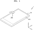
- FIG. 1 is a perspective view schematically illustrating a display apparatus according to an embodiment.
- a display apparatus 1 may include a display area DA and a non-display area NDA arranged around the display area DA.
- the non-display area NDA may surround the display area DA.
- the display apparatus 1 may provide an image by using light emitted from a plurality of pixels P arranged in the display area DA, and the non-display area NDA may be an area where no image is displayed. For example, a plurality of pixels P may not be arranged in the non-display area NDA to provide an image.
- the display apparatus 1 of embodiments of the present disclosure may be an inorganic light emitting display apparatus (or an inorganic electroluminescence (EL) display apparatus) or may be another display apparatus 1 such as a quantum dot light emitting display apparatus.
- an emission layer of a display element included in the display apparatus 1 may include an organic material, an inorganic material, quantum dots, an organic material and quantum dots, and/or an inorganic material and quantum dots.
- FIG. 1 illustrates the display apparatus 1 having a flat display surface
- the display apparatus 1 may include a three-dimensional display surface or a curved display surface.
- the display apparatus 1 may include a plurality of display areas indicating different directions (e.g., display areas facing different directions) and may include, for example, a polygonal columnar display surface.
- the display apparatus 1 when the display apparatus 1 includes a curved display surface, the display apparatus 1 may be implemented (or provided) in various suitable forms such as flexible, foldable, and/or rollable forms corresponding to flexible, foldable, and/or rollable display apparatuses respectively.
- FIG. 1 illustrates the display apparatus 1 that may be applied to a mobile phone terminal.
- a mobile phone terminal may be constructed by arranging electronic modules, a camera module, a power module, and the like mounted on a main board, in a bracket/case or the like together with (e.g., housed with) the display apparatus 1.
- the display apparatus 1 according to the present disclosure may be applied to large electronic apparatuses (e.g., televisions or monitors) and small and medium electronic apparatuses (e.g., tablets, car navigations, game machines, or smart watches).
- FIG. 1 illustrates a case where the display area DA of the display apparatus 1 is a tetragonal shape
- the shape of the display area DA may be any suitable shape including, for example, circular, elliptical, or polygonal (e.g., triangular or pentagonal) shapes.
- the display apparatus 1 may include a plurality of pixels P arranged in the display area DA.
- Each of the pixels P may include an organic light emitting diode OLED.
- Each pixel P may emit, for example, red, green, blue, or white light from the organic light emitting diode OLED.
- the "pixel P" may be understood as a pixel emitting any one of red light, green light, blue light, and white light.
- FIG. 2 is a plan view schematically illustrating a display apparatus according to an embodiment.
- the display apparatus 1 may include a plurality of pixels P arranged in the display area DA.
- Each of the pixels P may include a display element such as an organic light emitting diode OLED.
- Each pixel P may emit, for example, red, green, blue, or white light from the organic light emitting diode OLED.
- the "pixel P" may be understood as a pixel emitting any one of red light, green light, blue light, and white light.
- Each pixel P may be connected (e.g., electrically connected) to peripheral circuits arranged in the non-display area NDA.
- a first scan driving circuit 110, a first emission driving circuit 115, a second scan driving circuit 120, a terminal 140, a data driving circuit 150, a first power supply line 160, and a second power supply line 170 may be arranged in the non-display area NDA.
- the first scan driving circuit 110 may provide a scan signal to each pixel P through a scan line SL.
- the first emission driving circuit 115 may provide an emission control signal to each pixel P through an emission control line EL.
- the second scan driving circuit 120 may be arranged parallel to the first scan driving circuit 110 with the display area DA therebetween. Some of the pixels P arranged in the display area DA may be connected (e.g., electrically connected) to the first scan driving circuit 110, and the others may be connected (e.g., electrically connected) to the second scan driving circuit 120. In an embodiment, the second scan driving circuit 120 may be omitted.
- the first emission driving circuit 115 may be arranged on or in the non-display area NDA while being spaced apart from the first scan driving circuit 110 in the x direction. Also, in an embodiment, the first emission driving circuit 115 may be arranged alternately in the y direction with the first scan driving circuit 110. For example, the first emission driving circuit 115 may be alternately arranged and spaced apart from the first scan driving circuit 110 in the y direction.
- the terminal 140 may be arranged at one side of a substrate 100.
- the terminal 140 may be exposed, by not being covered by an insulating layer, and be connected (e.g., electrically connected) to a printed circuit board PCB.
- a contact of the terminal 140 may be exposed to connect (e.g., electrically connect) to the printed circuit board PCB (e.g., a terminal PCB-P of the printed circuit board PCB).
- a terminal PCB-P of the printed circuit board PCB may be connected (e.g., electrically connected) to the terminal 140 of the display apparatus 1.
- the printed circuit board PCB may be configured to transmit power or signals of a controller to the display apparatus 1.
- a control signal generated by the controller may be transmitted to each of the first scan driving circuit 110, the first emission driving circuit 115, and the second scan driving circuit 120 through the printed circuit board PCB.
- the controller may provide a first power voltage ELVDD and a second power voltage ELVSS to the first power supply line 160 and the second power supply line 170 through a first connection line 161 and a second connection line 171, respectively.
- the first power voltage ELVDD may be provided to each pixel P through a driving voltage line PL connected to the first power supply line 160
- the second power voltage ELVSS may be provided to an opposite electrode of each pixel P connected to the second power supply line 170.
- the first power voltage ELVDD may be a driving voltage
- the second power voltage ELVSS may be a common voltage.
- the data driving circuit 150 may be connected (e.g., electrically connected) to a data line DL.
- a data signal of the data driving circuit 150 may be provided to each pixel P through a connection line 151 connected to the terminal 140 and a data line DL connected to the connection line 151.
- FIG. 2 illustrates that the data driving circuit 150 is arranged on the printed circuit board PCB.
- the data driving circuit 150 may be arranged on the substrate 100.
- the data driving circuit 150 may be arranged between the terminal 140 and the first power supply line 160 on the substrate 100.
- the first power supply line 160 may include a first subline 162 and a second subline 163 extending in parallel in the x direction with the display area DA therebetween.
- the second power supply line 170 may partially surround the display area DA in a loop shape with one side open.
- the terminal 140 may be at the one open side of the loop shape of the second power supply line 170.
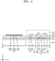
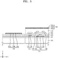
- FIGS. 3-8 are cross-sectional views schematically illustrating a method of manufacturing a display apparatus, according to an embodiment.
- a method of manufacturing a display apparatus may include an operation of forming a thin film transistor TFT on a substrate 100 of a display area DA, an operation of forming a planarization layer 113 on the thin film transistor TFT, an operation of forming an electrode layer 180 on the planarization layer 113, and an operation of forming a pixel electrode 210 by etching the electrode layer 180 with an etchant composition.
- the substrate 100 may include a glass material, a ceramic material, a metal material, and/or any flexible or bendable material.
- the substrate 100 may include a polymer resin such as polyethersulfone, polyacrylate, polyetherimide, polyethylene naphthalate, polyethylene terephthalate, polyphenylene sulfide, polyarylate, polyimide, polycarbonate, and/or cellulose acetate propionate.
- the substrate 100 may have a single-layer or multi-layer structure of the above-mentioned material, and in the case of the multi-layer structure, the substrate may further include an inorganic layer. In an embodiment, the substrate 100 may have an organic/inorganic/organic structure.
- a buffer layer 101 may be formed on the substrate 100.
- the buffer layer 101 may be on the substrate 100 to reduce or block the penetration of foreign materials, moisture, or external air from the bottom of the substrate 100.
- the buffer layer 101 may provide a flat surface on the substrate 100.
- the buffer layer 101 may include an inorganic material (e.g., oxide or nitride), an organic material, or an organic/inorganic composite and may include a single-layer or multi-layer structure of an inorganic material and an organic material.
- a thin film transistor TFT may be formed on the buffer layer 101.
- the thin film transistor TFT may include a semiconductor layer 134, a gate electrode 136, a source electrode 137, and a drain electrode 138.
- the thin film transistor TFT may be connected (e.g., electrically connected) to an organic light emitting diode OLED described in more detail below to drive the organic light emitting diode OLED.
- the semiconductor layer 134 may include a channel area 131 formed on the buffer layer 101 and overlapping the gate electrode 136.
- the semiconductor layer 134 may include a source area 132 and a drain area 133 arranged on respective sides of the channel area 131.
- the source area 132 and the drain area 133 may each include a higher concentration of impurities than the channel area 131.
- the impurities may include N-type impurities or P-type impurities.
- the source area 132 and the drain area 133 may be electrically and respectively connected to the source electrode 137 and the drain electrode 138 described in more detail below.
- the source area 132 may be connected (e.g., electrically connected) to the source electrode 137, and the drain area 133 may be connected (e.g., electrically connected) to the drain electrode 138.
- the source area 132 may overlap the source electrode 137 in the z direction, and the drain area 133 may overlap the drain electrode 138 in the z direction.
- the semiconductor layer 134 may include an oxide semiconductor and/or a silicon semiconductor.
- the semiconductor layer 134 may include, for example, an oxide of at least one of indium (In), gallium (Ga), stannum (Sn), zirconium (Zr), vanadium (V), hafnium (Hf), cadmium (Cd), germanium (Ge), chromium (Cr), titanium (Ti), or zinc (Zn).
- the semiconductor layer 134 may include InSnZnO (ITZO) or InGaZnO (IGZO).
- the semiconductor layer 134 may include, for example, amorphous silicon (a-Si) or low temperature poly-silicon (LTPS) crystallized from amorphous silicon (a-Si).
- a first insulating layer 103 may be formed on the semiconductor layer 134.
- the first insulating layer 103 may include an inorganic insulating material of at least one of silicon oxide (SiO 2 ), silicon nitride (SiN x ), silicon oxynitride (SiON), aluminum oxide (Al 2 O 3 ), titanium oxide (TiO 2 ), tantalum oxide (Ta 2 O 5 ), hafnium oxide (HfO 2 ), or zinc oxide (ZnO 2 ).
- the first insulating layer 103 may include a single-layer or a multi-layer structure including the above-mentioned inorganic insulating material.
- the gate electrode 136 may be formed on the first insulating layer 103.
- the gate electrode 136 may include a single-layer or a multi-layer structure formed of at least one of aluminum (Al), platinum (Pt), palladium (Pd), silver (Ag), magnesium (Mg), gold (Au), nickel (Ni), neodymium (Nd), iridium (Ir), chromium (Cr), lithium (Li), calcium (Ca), molybdenum (Mo), titanium (Ti), tungsten (W), or copper (Cu).
- the gate electrode 136 may be connected to a gate line such that an electrical signal may be applied to the gate electrode 136.
- a second insulating layer 105 may be formed on the gate electrode 136.
- the second insulating layer 105 may include an inorganic insulating material of at least one of silicon oxide (SiO 2 ), silicon nitride (SiN x ), silicon oxynitride (SiON), aluminum oxide (Al 2 O 3 ), titanium oxide (TiO 2 ), tantalum oxide (Ta 2 O 5 ), hafnium oxide (HfO 2 ), or zinc oxide (ZnO 2 ).
- the second insulating layer 105 may include a single-layer or a multi-layer structure including the above-mentioned inorganic insulating material.
- a storage capacitor Cst may be formed on the first insulating layer 103.
- the storage capacitor Cst may include a lower electrode 144 and an upper electrode 146 overlapping (e.g., overlapping in the z direction or in a plan view) the lower electrode 144.
- the lower electrode 144 and the upper electrode 146 of the storage capacitor Cst may overlap each other with the second insulating layer 105 therebetween.
- the lower electrode 144 and the upper electrode 146 of the storage capacitor Cst may overlap each other in the z direction (or in the plan view) and the second insulating layer 105 may be between the lower electrode 144 and the upper electrode 146 in the z-direction (or in the plan view).
- the lower electrode 144 of the storage capacitor Cst may overlap the gate electrode 136 of the thin film transistor TFT, and the lower electrode 144 of the storage capacitor Cst may be integrally provided with the gate electrode 136 of the thin film transistor TFT.
- the upper electrode 146 of the storage capacitor Cst may include aluminum (Al), platinum (Pt), palladium (Pd), silver (Ag), magnesium (Mg), gold (Au), nickel (Ni), neodymium (Nd), iridium (Ir), chromium (Cr), lithium (Li), calcium (Ca), molybdenum (Mo), titanium (Ti), tungsten (W), and/or copper (Cu) and may include a single-layer or a multi-layer structure of the above-mentioned material.
- a third insulating layer 107 may be formed on the upper electrode 146 of the storage capacitor Cst.
- the third insulating layer 107 may include an inorganic insulating material of at least one of silicon oxide (SiO 2 ), silicon nitride (SiN x ), silicon oxynitride (SiON), aluminum oxide (Al 2 O 3 ), titanium oxide (TiO 2 ), tantalum oxide (Ta 2 O 5 ), hafnium oxide (HfO 2 ), or zinc oxide (ZnO 2 ).
- the third insulating layer 107 may include a single-layer or a multi-layer structure including the above-mentioned inorganic insulating material.
- the source electrode 137 and the drain electrode 138 may be formed on the third insulating layer 107.
- the source electrode 137 and the drain electrode 138 may include a conductive material including molybdenum (Mo), aluminum (Al), copper (Cu), titanium (Ti), or the like and may include a single-layer or a multi-layer structure including the above-mentioned material.
- the source electrode 137 and the drain electrode 138 may include a multi-layer structure of Ti/Al/Ti.
- a line layer 139 may be formed on the third insulating layer 107 of the non-display area NDA by the same process.
- the line layer 139 may include the same material as the source electrode 137 or the drain electrode 138.
- the line layer 139 may include a first line layer 139a including a second metal, a second line layer 139b including a third metal, and a third line layer 139c including the second metal.
- the second metal and the third metal may include molybdenum (Mo), aluminum (Al), copper (Cu), titanium (Ti), or the like.
- the second metal may include titanium (Ti), and the third metal may include aluminum (Al).
- the line layer 139 may have a titanium (Ti)/aluminum (Al)/titanium (Ti) multi-layer structure.
- Lines arranged on the same layer as the semiconductor layer 134, the gate electrode 136, and the upper electrode 146 of the display area DA may be arranged under the line layer 139, but are omitted for convenience of description.
- the electrode layer 180 described in more detail below may be etched by an etchant composition with the top surface of the line layer 139 exposed.
- an operation of forming a planarization layer 113 on the thin film transistor TFT may be further performed.
- the planarization layer 113 may be formed on the source electrode 137 and the drain electrode 138.
- the planarization layer 113 may include a single-layer or a multi-layer structure formed of an organic material or an inorganic material.
- the planarization layer 113 may include a general-purpose polymer such as benzocyclobutene (BCB), polyimide (PI), hexamethyldisiloxane (HMDSO), polymethylmethacrylate (PMMA), or polystyrene (PS), a polymer derivative having a phenolic group, an acrylic polymer, an imide-based polymer, an arylether-based polymer, an amide-based polymer, a fluorine-based polymer, a p-xylene-based polymer, a vinyl alcohol-based polymer, or any blend thereof.
- BCB benzocyclobutene
- PI polyimide
- HMDSO hexamethyldisiloxane
- PMMA polymethylmeth
- the planarization layer 113 may include silicon oxide (SiO 2 ), silicon nitride (SiN x ), silicon oxynitride (SiON), aluminum oxide (Al 2 O 3 ), titanium oxide (TiO 2 ), tantalum oxide (Ta 2 O 5 ), and hafnium oxide (HfO 2 ), or zinc oxide (ZnO 2 ).
- chemical mechanical polishing may be performed to provide a flat upper surface.
- a contact metal layer may be formed on the planarization layer 113, and a planarization layer may be additionally formed on the contact metal layer.
- the electrode layer 180 may include a reflective layer formed of aluminum (Al), platinum (Pt), palladium (Pd), silver (Ag), magnesium (Mg), gold (Au), nickel (Ni), neodymium (Nd), iridium (Ir), chromium (Cr), lithium (Li), calcium (Ca), molybdenum (Mo), titanium (Ti), tungsten (W), copper (Cu), or any compound thereof and a transparent or semitransparent conductive layer formed on the reflective layer.
- the transparent or semitransparent electrode may include at least one of indium tin oxide (ITO), indium zinc oxide (IZO), zinc oxide (ZnO), indium oxide (In 2 O 3 ), indium gallium oxide (IGO), or aluminum zinc oxide (AZO).
- the electrode layer 180 may include a first conductive layer 180a, a second conductive layer 180b including a first metal and arranged on the first conductive layer 180a, and a third conductive layer 180c arranged on the second conductive layer 180b.
- the first conductive layer 180a and the third conductive layer 180c may include an indium tin oxide (ITO) that is a transparent or semitransparent conductive layer, and the first metal may include silver (Ag).
- the electrode layer 180 may include a stack structure of indium tin oxide (ITO)/silver (Ag)/indium tin oxide (ITO).
- an operation of forming a pixel electrode 210 by etching the electrode layer 180 with an etchant composition may be further performed.
- a photoresist pattern PR may be patterned on the electrode layer 180 and then the pixel electrode 210 may be formed by etching the electrode layer 180 by using the above-mentioned etchant composition.
- the photoresist pattern PR may be patterned on the electrode layer 180 prior to applying the etchant composition to form the pixel electrode 210 by etching the electrode layer 180.
- the pixel electrode 210 may include a first layer 210a, a second layer 210b, and a third layer 210c.
- the first layer 210a, the second layer 210b, and the third layer 210c of the pixel electrode 210 may respectively correspond to the first conductive layer 180a, the second conductive layer 180b, and the third conductive layer 180c of the electrode layer 180.
- the first layer 210a, the second layer 210b, and the third layer 210c may be formed by etching the first conductive layer 180a, the second conductive layer 180b, and the third conductive layer 180c respectively.
- the first layer 210a and the third layer 210c of the pixel electrode 210 may include indium tin oxide (ITO), and the second layer 210b may include silver (Ag).
- the pixel electrode 210 may include a stack structure of indium tin oxide (ITO)/silver (Ag)/indium tin oxide (ITO).
- the pixel electrode 210 may be formed by etching the electrode layer 180 including, in an embodiment, a multi-layer structure such as indium tin oxide (ITO)/silver (Ag)/indium tin oxide (ITO) by using an etchant composition according to an embodiment.
- a multi-layer structure such as indium tin oxide (ITO)/silver (Ag)/indium tin oxide (ITO) by using an etchant composition according to an embodiment.
- Various lines and electrodes included in the display apparatus may include silver (Ag).
- a line or electrode including silver (Ag) has a weak bonding strength with a layer or film located over or under (e.g., directly on) the line or electrode include silver (Ag)
- the line or electrode may include a multi-layer structure including a stack of a layer including silver (Ag) and other conductive layers.
- the stack may include silver (Ag) between other conductive layers.
- various lines and electrodes included in the display apparatus may be formed by using a patterning process such as photolithography including an etching process, and when the lines or electrodes include multiple layers having different properties, there may be a limit in forming lines or electrodes having desired or suitable characteristics by a concurrent (e.g., simultaneous) etching process.
- an etchant of the related art used to etch a line may include phosphoric acid
- other lines in a display apparatus may be damaged by the phosphoric acid during the etching process and silver ions may be reduced and precipitated through this process, and accordingly, defects may occur (or be introduced) due to silver particles.
- a multi-layer structure including silver (Ag) and other conductive layers may be sequentially etched.
- the above-mentioned method e.g., method including sequential etching
- additional processing steps or tasks may be needed which may decrease efficiency (e.g., throughput) of the manufacturing process.
- the etchant composition according to an embodiment may prevent or substantially prevent silver (Ag) ions from being reduced and precipitated while collectively etching an electrode layer including a multi-layer structure such as indium tin oxide (ITO)/silver (Ag)/indium tin oxide (ITO). Accordingly, the reliability of the display apparatus may be improved. Further, efficiency (e.g., throughput) may be improved compared to sequential etching.
- the etchant composition according to an embodiment may include an inorganic acid compound of about 8 wt% to about 15 wt%, a sulfonic acid compound of about 2.5 wt% to about 8 wt%, a sulfate compound of about 6 wt% to about 14 wt%, an organic acid compound of about 40 wt% to about 55 wt%, a metal or metal salt of about 0.01 wt% to about 0.06 wt%, and a remaining amount of water.
- the inorganic acid compound may include a nitric acid.
- the nitric acid may be a component used as an oxidizer and may be used to etch silver (Ag) and other conductive layers.
- the nitric acid may be used to oxidize and wet-etch silver (Ag) and other conductive layers.
- the content of the nitric acid may be about 8 wt% to about 15 wt% in the total weight of the etchant composition.
- the etch rate of the other conductive layers may be accelerated and thus an undercut may occur in the other conductive layers located over and/or under silver (Ag), which may cause a problem in a subsequent process.
- the etch rate of the silver (Ag) and the other conductive layers may be reduced and thus the etching uniformity may be reduced depending on the position of the substrate, which may cause a stain.
- the etch rate may be easily controlled (e.g., more easily controlled) and the silver (Ag) and the other conductive layers may be uniformly or substantially uniformly etched.
- the sulfonic acid compound may include at least one of a methanesulfonic acid, an ethanesulfonic acid, or a propanesulfonic acid.
- the sulfonic acid compound may be used as an etchant for etching the silver (Ag) and conductive layers oxidized with the nitric acid.
- the sulfonic acid compound may maintain a constant or substantially constant etch rate by reducing the decomposition rate of the nitric acid.
- the content of the sulfonic acid compound may be about 2.5 wt% to about 8 wt% in the total weight of the etchant composition.
- the effect of inhibiting the decomposition of the nitric acid may be reduced and thus the stability may be reduced and a silver (Ag) residue may occur.
- the sulfonic acid compound of about 2.5 wt% to about 8 wt% is included in the etchant composition, the etch rate of the silver (Ag) and conductive layers may be easily controlled and a defect due to the occurrence of a silver (Ag) residue and silver (Ag) resorption may be prevented or substantially prevented.
- the sulfate compound may include at least one of a potassium hydrogen sulfate, a sodium hydrogen sulfate, or an ammonium hydrogen sulfate.
- the sulfate compound may be used as an etchant for etching the conductive layer.
- the sulfate compound may cause an etch stop of silver (Ag).
- the etch stop may mean that a skew, which is the distance between the photoresist pattern end and the silver (Ag) end, may not increase even when time elapses (e.g., additional time elapses where the silver (Ag) is exposed to the etchant composition including the sulfate compound).
- time elapses e.g., additional time elapses where the silver (Ag) is exposed to the etchant composition including the sulfate compound.
- the etch stop characteristics may be implemented and the etch rate may be controlled and accordingly the side etch may be controlled.
- the content of the sulfate compound may be about 6 wt% to about 14 wt% in the total weight of the etchant composition.
- the etch rate of the conductive layer may be too high and thus a corrosion failure may be induced.
- the etch rate of the conductive layer may decrease and thus a residue of silver (Ag) and the other conductive layers may occur.
- the etch rate may be easily controlled and the etch stop characteristics may be implemented and thus the silver (Ag) and the other conductive layers may be uniformly etched.
- the organic acid compound may include at least one of an acetic acid, a citric acid, a glycolic acid, a malonic acid, a lactic acid, or a tartaric acid.
- the organic acid compound may include an acetic acid and a citric acid.
- the organic acid compound may be used as an etchant for etching the silver (Ag).
- the organic acid compound may be used to etch the silver (Ag) oxidized by the nitric acid described above.
- the content of the organic acid compound may be about 40 wt% to about 55 wt% in the total weight of the etchant composition.
- the content of the organic acid compound is less than about 40 wt%, a stain may occur due to a non-uniform etch rate depending on the position of the substrate.
- the content of the organic acid compound is more than about 55 wt%, an over-etching problem may occur.
- the organic acid compound of about 40 wt% to about 55 wt% is included in the etchant composition, the etch rate of silver (Ag) may be controlled (e.g., easily controlled) and a defect due to the occurrence of a silver (Ag) residue and resorption may be prevented or be substantially prevent.
- the metals or metal salt may include a metal such as iron (Fe) or copper (Cu) or a metal salt such as iron (Fe), copper (Cu), aluminum (Al), molybdenum (Mo), chromium (Cr), or manganese (Mn).
- the metal or metal salt may include at least one of a ferric nitrate, a ferric sulfate, copper, a copper sulfate, or iron.
- the metal or metal salt may be used as an oxidizer of silver (Ag).
- the metal or metal salt may be used as an auxiliary oxidizer of the nitric acid described above.
- the content of the metal or metal salt may be about 0.01 wt% to about 0.06 wt% in the etchant composition.
- the etching uniformity may be reduced.
- the content of the metal or metal salt is more than about 0.06 wt%, the etch stop characteristics may be degraded.
- the metal or metal salt of about 0.01 wt% to about 0.06 wt% is included in the etchant composition, the etch rate of silver (Ag) may be easily controlled, a defect due to a silver (Ag) residue and silver (Ag) resorption may be prevented or be substantially prevented, and the etch stop characteristics may be improved.
- the etchant composition may include water.
- the water may be included in the etchant composition such that the sum of the wt% of components other than the water and the wt% of the water may be 100 wt%.
- Ultrapure water may be used as the water included in the etchant composition.
- the water included in the etchant composition may function to activate the sulfate compound.
- the content of the water may be about 28 wt% to about 30 wt% in the etchant composition.
- the etch stop characteristics may be degraded.
- the content of the water is more than about 30 wt%, there may be a problem such as the occurrence of a silver residue.
- the water of about 28 wt% to about 30 wt% is included in the etchant composition, a defect due to a silver residue may be prevented or be substantially prevented and the etch stop characteristics may be implemented.
- the wt% ratio of the sulfate compound to the organic acid compound may be about 1:4 to about 1:5.
- the etch stop characteristics may be maintained even when the number of treatments is accumulated as well as at initial etching, and thus the side etch may be controlled.
- the side etch may be more effectively controlled.
- Embodiments 1 to 4 Embodiment 1, Embodiment 2, Embodiment 3, and Embodiment 4
- Comparative Examples 1 to 7 Comparative Example 1, Comparative Example 2, Comparative Example 3, Comparative Example 4, Comparative Example 5, Comparative Example 6, and Comparative Example 7
- Table 1 The % in Table 1 below may be wt%.
- Comparative Example 1 and Comparative Example 2 may respectively correspond to the cases where the ratio of the sulfate compound to the organic acid compound is about 1:3.9 and about 1:5.2 deviating from a weight ratio of about 1:4 to about 1:5, Comparative Example 3 may correspond to the case where the content of the organic acid compound is less than about 40 wt% and the content of the sulfate compound is less than about 6 wt%, and Comparative Example 4 may correspond to the case where the content of the organic acid compound is more than about 55 wt%.
- Comparative Example 5 may correspond to the case where no metal or metal salt is added
- Comparative Example 6 may correspond to the case where the content of the metal or metal salt is more than about 0.06 wt%
- Comparative Example 7 may correspond to the case where the content of the water is less than about 28 wt%.
- an etching process was performed by using a first etchant and a second etchant.
- the first etchant may correspond to the etchant composition of Embodiments 1 to 4 and Comparative Examples 1 to 7
- the second etchant may correspond to the etchant obtained by dissolving silver powders in the etchant composition of Embodiments 1 to 4 and Comparative Examples 1 to 7, assuming that an etching process was performed for a long time.
- the spray-etching test equipment Model name: ETCHER(TFT), SEMES
- the temperature was set to 40 °C causing a rise in temperature
- an etching process was performed on the specimen when the temperature reached 40 °C ⁇ 0.1 °C.
- the specimen was additionally over-etched by 50 % and 100 % from the time when the etching of the specimen was ended (e.g., the etching time was increased by 50% and 100%), and the side etch resulting from each of 50% over-etching and 100% over-etching was measured by using an electron scanning microscope (Model name: SU-8010, HITACHI).
- the side etch may correspond to the distance from the end of the patterned photoresist to the etched silver (Ag).
- a suitable range of the side etch may be less than about 0.3 ⁇ m.
- the side etch exceeds about 0.3 ⁇ m, it may be considered or categorized as a defect.
- the etch stop may be determined as good when the side etch change of 100% over-etching compared to 50% over-etching is less than about 0.05 ⁇ m.
- the etch stop may be considered as poor when the side etch change of 100% over-etching compared to 50% over-etching exceeds about 0.05 ⁇ m.
- the electron scanning microscope (Model name: SU-8010, HITACHI) was used to measure a residue that is a phenomenon in which silver (Ag) and indium tin oxide (ITO) remain unetched in a region not covered by the photoresist (e.g., not covered by the photoresist during the etching process and prior to the photoresist being stripped by the photoresist stripper).
- a residue that is a phenomenon in which silver (Ag) and indium tin oxide (ITO) remain unetched in a region not covered by the photoresist (e.g., not covered by the photoresist during the etching process and prior to the photoresist being stripped by the photoresist stripper).
- ITO indium tin oxide
- the electron scanning microscope (Model name: SU-8010, HITACHI) (Ag) was used to measure the number of silver (Ag) particles adsorbed onto the upper titanium (Ti) of the titanium (Ti)/aluminum (Al)/titanium (Ti) triple layer exposed in the specimen.
- the measured number of silver (Ag) particles was about 10 or less, it was evaluated as good, and when the measured number of silver (Ag) particles was more than about 10, it was evaluated as poor.
- FIG. 9A is a diagram illustrating a state in which a metal pattern is formed by using an etchant composition according to an embodiment
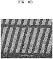
- FIG. 9B is a diagram illustrating a state in which a metal pattern is formed after adding 1000 ppm of silver (Ag) to an etchant composition according to an embodiment
- FIG. 9B is a diagram illustrating a state in which a metal pattern is formed after adding 1000 ppm of silver (Ag) to an etchant composition, in order to check the etching characteristics depending on the number of treatments of an etchant composition according to an embodiment.
- silver (Ag) particles are effectively not or hardly precipitated even when the number of treatments of the etchant composition according to an embodiment is increased.
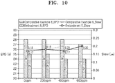
- FIG. 10 is a graph illustrating end point detection (EPD) and skew depending on the number of treatments of an etchant composition according to an embodiment and an etchant composition according to a comparative example. More particularly, FIG. 10 is a graph illustrating EPD and skew depending on the number of treatments of an etchant composition according to an embodiment (Embodiment 5) and an etchant composition of the related art (Comparative Example 8).
- EPD end point detection
- FIG. 10 is a graph illustrating EPD and skew depending on the number of treatments of an etchant composition according to an embodiment (Embodiment 5) and an etchant composition of the related art (Comparative Example 8).
- the etchant composition of the related art may be an etchant composition including a phosphoric acid-based composition
- the etchant composition according to an embodiment may be an etchant composition including an inorganic acid compound of about 8 wt% to about 15 wt%, a sulfonic acid compound of about 2.5 wt% to about 8 wt%, a sulfate compound of about 6 wt% to about 14 wt%, an organic acid compound of about 40 wt% to about 55 wt%, a metal or metal salt of about 0.01 wt% to about 0.06 wt%, and a remaining amount of water.
- the EPD satisfies a range of about 27 to about 28 and the skew satisfies about 0.18 to about 0.20.
- the actual number of treatments of the etchant composition of the related art may be at most only about 300 due to the defect caused by silver (Ag) particles.
- the EPD satisfies a range of about 24 to about 25 and the skew satisfies about 0.17 to about 0.20. That is, it may be seen that the physical properties desired for the etchant composition are maintained constant even when the concentration of silver (Ag) ions is increased as the etchant composition according to an embodiment (Embodiment 5) is used multiple times.
- the number of treatments may be improved by about 3 times compared to the etchant composition of the related art.
- the etchant composition according to an embodiment has a smaller EPD than the etchant composition of the related art (Comparative Example 8)
- the time required for the etching process may be reduced to improve the efficiency (e.g., throughput) of the manufacturing process of the display apparatus.
- the etchant composition according to an embodiment is used to etch a multi-layer structure (e.g., a triple layer) of indium tin oxide (ITO)/silver (Ag)/indium tin oxide (ITO)
- a mouse bite may occur in a portion of the upper indium tin oxide (ITO) due to non-uniform formation of the upper indium tin oxide (ITO) and impurities such as dust and the silver (Ag) may be partially etched because the etchant composition permeates through a pin hole formed by the mouse bite.
- an etchant composition may be used to etch a multi-layer structure (e.g., a triple layer) of indium tin oxide (ITO)/silver (Ag)/indium tin oxide (ITO), wherein the upper indium tin oxide (ITO) may be etched by a separate etchant and then the silver (Ag)/indium tin oxide (ITO) may be etched by the etchant composition according to an embodiment, thereby preventing or substantially prevent a mouse bite from occurring.
- ITO indium tin oxide
- ITO silver
- ITO indium tin oxide
- an etching process was performed by using an etchant composition including a first organic acid compound of about 18 wt% to about 25 wt%, a second organic acid compound of about 15 wt% to about 20 wt%, an inorganic acid compound of about 8.1 wt% to about 9.9 wt%, a sulfonic acid compound of about 1 wt% to about 4.9 wt%, a hydrogen sulfate compound of about 10 wt% to about 20 wt%, a nitrogen-containing dicarbonyl compound of about 1 wt% to about 5 wt%, an amino acid derivative compound of about 1 wt% to about 5 wt%, an iron-containing oxidizer compound of about 0.1 wt% to about 2 wt%, and a remaining amount of water.
- an etchant composition including a first organic acid compound of about 18 wt% to about 25 wt%, a second organic acid compound of about 15 wt% to about 20
- the etchant composition of the related art may include an iron-containing oxidizer compound of about 0.1 wt% to about 2 wt% to prevent or substantially prevent the occurrence of a silver (Ag) residue.
- an iron-containing oxidizer compound of about 0.1 wt% to about 2 wt% to prevent or substantially prevent the occurrence of a silver (Ag) residue.
- the etchant composition of the related art may include a nitrogen-containing dicarbonyl compound and an amino acid derivative compound.
- the nitrogen-containing dicarbonyl compound and the amino acid derivative compound included in the etchant composition of the related art may function as a corrosion inhibitor.
- the nitrogen-containing dicarbonyl compound and the amino acid derivative compound included in the etchant composition of the related art may form a complex compound with a metal to function as an etching controller for silver (Ag), indium tin oxide (ITO), and aluminum (Al).
- a silver (Ag) residue may occur.
- the etchant composition according to an embodiment may implement an etch stop by controlling the content of the sulfate compound and the water even without including the nitrogen-containing dicarbonyl compound and the amino acid derivative compound, thereby making it possible to prevent or reduce excessive etching to implement a low skew and provide a high-resolution display apparatus.
- an operation of forming an intermediate layer 220 on the pixel electrode 210 and an opposite electrode 230 on the intermediate layer 220 may be further performed.
- the pixel electrode 210, the intermediate layer 220, and the opposite electrode 230 may form an organic light emitting diode OLED.
- a pixel definition layer 190 may be formed on the planarization layer 113, and the pixel definition layer 190 may have an opening for exposing at least a portion of the pixel electrode 210.
- the area exposed by the opening of the pixel definition layer 190 may be defined as an emission area.
- the periphery of emission areas may be a non-emission area, and the non-emission area may surround the emission areas. That is, the display area DA may include a plurality of emission areas and a non-emission area surrounding the emission areas.
- the pixel definition layer 190 may increase the distance between the pixel electrode 210 and the opposite electrode 230 over the pixel electrode 210 to prevent or substantially prevent an arc or the like from occurring at the edge of the pixel electrode 210.
- the pixel definition layer 190 may be formed of an organic insulating material such as polyimide, polyamide, acrylic resin, benzocyclobutene, hexamethyldisiloxane (HMDSO), or phenol resin by spin coating or the like.
- organic insulating material such as polyimide, polyamide, acrylic resin, benzocyclobutene, hexamethyldisiloxane (HMDSO), or phenol resin by spin coating or the like.
- the intermediate layer 220 may be arranged on the pixel electrode 210 at least partially exposed by the pixel definition layer 190.
- the intermediate layer 220 may include an emission layer, and a first functional layer and a second functional layer may be selectively arranged under and over the emission layer.
- the intermediate layer 220 may be arranged on the pixel electrode 210 that is at least partially exposed by the pixel definition layer 190. More particularly, the emission layer of the intermediate layer 220 may be arranged on the pixel electrode 210 that is at least partially exposed by the pixel definition layer 190.
- a first functional layer may be formed under the emission layer, and a second functional layer may be formed over the emission layer.
- the first functional layer and the second functional layer respectively arranged under and over the emission layer may be collectively referred to organic functional layers.
- the first functional layer may include a hole injection layer (HIL) and/or a hole transport layer (HTL), and the second functional layer may include an electron transport layer (ETL) and/or an electron injection layer (EIL).
- HIL hole injection layer
- HTL hole transport layer
- ETL electron transport layer
- EIL electron injection layer
- the emission layer may include an organic material including a fluorescent or phosphorescent material emitting red, green, blue, or white light.
- the emission layer may include a low-molecular weight organic material or a high-molecular weight organic material.
- the intermediate layer 220 may include a structure in which a hole injection layer, a hole transport layer, an emission layer, and an electron transport layer, an electron injection layer, and the like are stacked in a single or complex structure and the low-molecular weight organic material may include various suitable organic materials such as copper phthalocyanine (CuPc), N,N'-di(naphthalene-1-yl)-N,N'-diphenyl-benzidine(NPB), and/or tris-8-hydroxyquinoline aluminum (Alq3). These layers may be formed by vacuum deposition.
- CuPc copper phthalocyanine
- NPB N,N'-di(naphthalene-1-yl)-N,N'-diphenyl-benzidine
- Alq3 tris-8-hydroxyquinoline aluminum
- the intermediate layer 220 may generally have a structure including a hole transport layer and an emission layer.
- the hole transport layer may include poly(3,4-ethylenedioxythiophene) (PEDOT) and the emission layer may include a high-molecular weight material such as poly-phenylene vinylene (PPV) and/or polyfluorene.
- PEDOT poly(3,4-ethylenedioxythiophene)
- the emission layer may include a high-molecular weight material such as poly-phenylene vinylene (PPV) and/or polyfluorene.
- the emission layer may be formed by screen printing, inkjet printing, laser induced thermal imaging (LITI), or the like.
- the opposite electrode 230 may be formed on the intermediate layer 220.
- the opposite electrode 230 may be formed on the intermediate layer 220 and may be formed to entirely cover the intermediate layer 220.
- the opposite electrode 230 may be formed over the display area DA and may be formed to entirely cover the intermediate layer 220. That is, by using an open mask, the opposite electrode 230 may be integrally formed over the entire display area to cover a plurality of pixels P arranged in the display area DA.
- the opposite electrode 230 may include a conductive material having a low work function.
- the opposite electrode 230 may include a (semi)transparent layer including silver (Ag), magnesium (Mg), aluminum (Al), platinum (Pt), palladium (Pd), gold (Au), nickel (Ni), neodymium (Nd), iridium (Ir), chromium (Cr), lithium (Li), calcium (Ca), or any alloy thereof.
- the opposite electrode 230 may further include a layer such as ITO, IZO, ZnO, or In 2 O 3 on the (semi)transparent layer including the above-mentioned material.
- embodiments may provide an etchant composition
- embodiments may provide an etchant composition substantially consisting of an inorganic acid compound of about 8 wt% to about 15 wt%; a sulfonic acid compound of about 2.5 wt% to about 8 wt%; a sulfate compound of about 6 wt% to about 14 wt%; an organic acid compound of about 40 wt% to about 55 wt%; a metal or metal salt of about 0.01 wt% to about 0.06 wt%; and water.
- Embodiments may provide an method of manufacturing a display apparatus comprising a display area and a non-display area, the method comprising: forming a thin film transistor on a substrate of the display area; forming a planarization layer on the thin film transistor; forming an electrode layer on the planarization layer; and forming a pixel electrode by etching the electrode layer with an etchant composition, wherein the etchant composition comprises: an inorganic acid compound of about 8 wt% to about 15 wt%; a sulfonic acid compound of about 2.5 wt% to about 8 wt%; a sulfate compound of about 6 wt% to about 14 wt%; an organic acid compound of about 40 wt% to about 55 wt%; a metal or metal salt of about 0.01 wt% to about 0.06 wt%; and water (which may form the remainder).
- the etchant composition comprises: an inorganic acid compound of about 8 wt% to about 15
- an etchant may not include a phosphoric acid, and the precipitation of silver may be prevented or reduced in the process of etching a multi-layer structure including a silver layer.
- the scope of the present disclosure is not limited to these effects.
Landscapes
- Chemical & Material Sciences (AREA)
- Engineering & Computer Science (AREA)
- Materials Engineering (AREA)
- Organic Chemistry (AREA)
- Manufacturing & Machinery (AREA)
- General Chemical & Material Sciences (AREA)
- Mechanical Engineering (AREA)
- Metallurgy (AREA)
- Chemical Kinetics & Catalysis (AREA)
- Inorganic Chemistry (AREA)
- Microelectronics & Electronic Packaging (AREA)
- Physics & Mathematics (AREA)
- Optics & Photonics (AREA)
- Electroluminescent Light Sources (AREA)
- Devices For Indicating Variable Information By Combining Individual Elements (AREA)
- Weting (AREA)
- ing And Chemical Polishing (AREA)
Abstract
Description
- This application claims priority to and the benefit of
Korean Patent Application No. 10-2020-0052900, filed on April 29, 2020 - One or more embodiments relate to an etchant composition and a method of manufacturing a display apparatus by using the same, and more particularly, to an etchant composition having improved reliability and a method of manufacturing a display apparatus by using the same.
- With the development of the display field representing various electrical signal information, various flat panel display apparatuses having excellent characteristics such as slimness, lightweight, and low power consumption have been researched and developed. Among them, organic light emitting display apparatuses have attracted attention as next-generation display apparatuses due to their advantages such as wide viewing angle and fast response time as well as lightweight and slimness.
- Moreover, as the display area of display apparatuses gradually increases, various lines and electrodes included in the display apparatuses may be formed of a material having low resistivity.
- Aspects of one or more embodiments are directed towards an etchant composition capable of etching a multi-layer structure including silver and a method of manufacturing a display apparatus by using the etchant composition. However, these problems are merely examples and the scope of the present disclosure is not limited thereto.
- Additional aspects will be set forth in part in the description which follows and, in part, will be apparent from the description, or may be learned by practice of the presented embodiments.
- According to one or more embodiments, an etchant composition includes an inorganic acid compound of about 8 wt% to about 15 wt%, a sulfonic acid compound of about 2.5 wt% to about 8 wt%, a sulfate compound of about 6 wt% to about 14 wt%, an organic acid compound of about 40 wt% to about 55 wt%, a metal or metal salt of about 0.01 wt% to about 0.06 wt%, and water.
- In the present embodiments, the inorganic acid compound may include a nitric acid.
- In the present embodiments, the sulfonic acid compound may include at least one of a methanesulfonic acid, an ethanesulfonic acid, or a propanesulfonic acid.
- In the present embodiments, the sulfate compound may include at least one of a potassium hydrogen sulfate, a sodium hydrogen sulfate, or an ammonium hydrogen sulfate.
- In the present embodiments, the organic acid compound may include at least one of an acetic acid, a citric acid, a glycolic acid, a malonic acid, a lactic acid, or a tartaric acid.
- In the present embodiments, the metal or metal salt may include at least one of a ferric nitrate, a ferric sulfate, a copper, a copper sulfate, or an iron.
- In the present embodiments, a wt% ratio of the sulfate compound to the organic acid compound may be about 1:4 to about 1:5.
- In the present embodiments, the water may be about 28 wt% to about 30 wt%.
- According to one or more embodiments, a method of manufacturing a display apparatus including a display area and a non-display area, the method includes forming a thin film transistor on a substrate of the display area, forming a planarization layer on the thin film transistor, forming an electrode layer on the planarization layer, and forming a pixel electrode by etching the electrode layer with an etchant composition, wherein the etchant composition includes an inorganic acid compound of about 8 wt% to about 15 wt%, a sulfonic acid compound of about 2.5 wt% to about 8 wt%, a sulfate compound of about 6 wt% to about 14 wt%, an organic acid compound of about 40 wt% to about 55 wt%, a metal or metal salt of about 0.01 wt% to about 0.06 wt%, and water.
- In the present embodiments, the electrode layer may be formed as a multi-layer structure.
- In the present embodiments, the electrode layer may include a first conductive layer, a second conductive layer including a first metal, and a third conductive layer. The first conductive layer and the third conductive layer may be transparent or semitransparent electrodes.
- In the present embodiments, the first metal may be silver.
- In the present embodiments, the etchant composition may be used to etch the first conductive layer, the second conductive layer, and the third conductive layer.
- In the present embodiments, the etchant composition may be used to etch the first conductive layer and the second conductive layer.
- In the present embodiments, the method may further include forming a line layer in the non-display area, wherein the electrode layer may be etched by the etchant composition with the line layer exposed.
- In the present embodiments, the line layer may include a first line layer including a second metal, a second line layer including a third metal, and a third line layer including the second metal.
- In the present embodiments, the second metal may be titanium, and the third metal may be aluminum.
- In the present embodiments, the thin film transistor may include a semiconductor layer, a gate electrode, a source electrode, and a drain electrode, and the line layer may be formed of the same material as the source electrode or the drain electrode.
- In the present embodiments, the method may further include forming an intermediate layer on the pixel electrode and an opposite electrode on the intermediate layer.
- In the present embodiments, the inorganic acid compound may include a nitric acid.
- In the present embodiments, the sulfonic acid compound may include at least one of a methanesulfonic acid, an ethanesulfonic acid, or a propanesulfonic acid.
- In the present embodiments, the sulfate compound may include at least one of a potassium hydrogen sulfate, a sodium hydrogen sulfate, or an ammonium hydrogen sulfate.
- In the present embodiments, the organic acid compound may include at least one of an acetic acid, a citric acid, a glycolic acid, a malonic acid, a lactic acid, or a tartaric acid.
- In the present embodiments, the metal or metal salt may include at least one of a ferric nitrate, a ferric sulfate, a copper, a copper sulfate, or an iron.
- In the present embodiments, a wt% ratio of the sulfate compound to the organic acid compound may be about 1:4 to about 1:5.
- In the present embodiments, the water may be about 28 wt% to about 30 wt%.
- According to an aspect, there is provided an etchant composition as set out in
claim 1. Additional features are provided in claims 2 to 8. - According to an aspect, there is provided method as set out in claim 9. Additional features are provided in claims 10 to 15.
- Other aspects, features, and advantages other than those described above will become apparent from the following detailed description, the appended claims, and the accompanying drawings.
- The above and other aspects, features, and advantages of certain embodiments will be more apparent from the following description taken in conjunction with the accompanying drawings, in which:
-
FIG. 1 is a perspective view schematically illustrating a display apparatus according to an embodiment; -
FIG. 2 is a plan view schematically illustrating a display apparatus according to an embodiment; -
FIGS. 3-8 are cross-sectional views schematically illustrating a method of manufacturing a display apparatus, according to an embodiment; -
FIG. 9A is a diagram illustrating a state in which a metal pattern is formed by using an etchant composition according to an embodiment; -
FIG. 9B is a diagram illustrating a state in which a metal pattern is formed after adding 1000 ppm of silver (Ag) to an etchant composition according to an embodiment; and -
FIG. 10 is a graph illustrating end point detection (EPD) and skew depending on the number of treatments of an etchant composition according to an embodiment and an etchant composition according to a comparative example. - Reference will now be made in detail to embodiments, examples of which are illustrated in the accompanying drawings, wherein like reference numerals refer to like elements throughout. In this regard, the present embodiments may have different forms and should not be construed as being limited to the descriptions set forth herein. Accordingly, the embodiments are merely described below, by referring to the figures, to explain aspects of the present description. As used herein, the term "and/or" includes any and all combinations of one or more of the associated listed items. Throughout the present disclosure, the expression "at least one of a, b or c" indicates only a, only b, only c, both a and b, both a and c, both b and c, all of a, b, and c, or variations thereof.
- The present disclosure may include various embodiments and modifications, and certain embodiments thereof are illustrated in the drawings and will be described herein in detail. The effects and features of the present disclosure and the accomplishing methods thereof will become apparent from the embodiments described below in detail with reference to the accompanying drawings. However, the present disclosure is not limited to the embodiments described below and may be embodied in various modes.
- It will be understood that although terms such as "first" and "second" may be used herein to describe various components, these components should not be limited by these terms and these terms are only used to distinguish one component from another component.
- As used herein, the singular forms "a," "an," and "the" are intended to include the plural forms as well, unless the context clearly indicates otherwise.
- Also, it will be understood that the terms "comprise," "include," and "have" used herein specify the presence of stated features or components, but do not preclude the presence or addition of one or more other features or components.
- It will be understood that when a layer, region, or component is referred to as being "on" another layer, region, or component, it may be "directly on" the other layer, region, or component or may be "indirectly on" the other layer, region, or component with one or more intervening layers, regions, or components therebetween.
- Sizes of components in the drawings may be exaggerated for convenience of description. In other words, because the sizes and thicknesses of components in the drawings are arbitrarily illustrated for convenience of description, embodiments of the present disclosure are not limited thereto.
- As used herein, "A and/or B" represents the case of A, B, or A and B. In the following embodiments, a line "extending in a first direction or a second direction" may include not only extending in a linear shape but also extending in a zigzag or curved shape along the first direction or the second direction.
- In the following embodiments, when referred to as "in a plan view," it may mean that a target portion is viewed from above, and when referred to as "in a cross-sectional view," it may mean that a cross-section of a target portion vertically cut is viewed from side. In the following embodiments, when referred to as "overlapping," it may include overlapping "in a plan view" and overlapping "in a cross-sectional view."
- As used herein, the terms "substantially," "about," and similar terms are used as terms of approximation and not as terms of degree, and are intended to account for the inherent deviations in measured or calculated values that would be recognized by those of ordinary skill in the art.
- Any numerical range recited herein is intended to include all sub-ranges of the same numerical precision subsumed within the recited range. For example, a range of "1.0 to 10.0" is intended to include all subranges between (and including) the recited minimum value of 1.0 and the recited maximum value of 10.0, that is, having a minimum value equal to or greater than 1.0 and a maximum value equal to or less than 10.0, such as, for example, 2.4 to 7.6. Any maximum numerical limitation recited herein is intended to include all lower numerical limitations subsumed therein and any minimum numerical limitation recited in this specification is intended to include all higher numerical limitations subsumed therein. Accordingly, Applicant reserves the right to amend this specification, including the claims, to expressly recite any sub-range subsumed within the ranges expressly recited herein.
- Further, the use of "may" when describing embodiments of the present disclosure refers to "one or more embodiments of the present disclosure". As used herein, the terms "use," "using," and "used" may be considered synonymous with the terms "utilize," "utilizing," and "utilized," respectively.
- Unless otherwise defined, all terms (including technical and scientific terms) used herein have the same meaning as commonly understood by one of ordinary skill in the art to which this disclosure is a part. Terms, such as those defined in commonly used dictionaries, should be interpreted as having a meaning that is consistent with their meaning in the context of the relevant art and should not be interpreted in an idealized or overly formal sense, unless expressly so defined herein.
- Hereinafter, embodiments will be described in detail with reference to the accompanying drawings, and in the following description, like reference numerals will denote like elements.
-
FIG. 1 is a perspective view schematically illustrating a display apparatus according to an embodiment. - Referring to
FIG. 1 , adisplay apparatus 1 may include a display area DA and a non-display area NDA arranged around the display area DA. The non-display area NDA may surround the display area DA. Thedisplay apparatus 1 may provide an image by using light emitted from a plurality of pixels P arranged in the display area DA, and the non-display area NDA may be an area where no image is displayed. For example, a plurality of pixels P may not be arranged in the non-display area NDA to provide an image. - Hereinafter, an organic light emitting display apparatus will be described as an example of the
display apparatus 1 according to an embodiment. However, thedisplay apparatus 1 of embodiments of the present disclosure is not limited thereto. In an embodiment, thedisplay apparatus 1 of the present disclosure may be an inorganic light emitting display apparatus (or an inorganic electroluminescence (EL) display apparatus) or may be anotherdisplay apparatus 1 such as a quantum dot light emitting display apparatus. For example, an emission layer of a display element included in thedisplay apparatus 1 may include an organic material, an inorganic material, quantum dots, an organic material and quantum dots, and/or an inorganic material and quantum dots. - Although
FIG. 1 illustrates thedisplay apparatus 1 having a flat display surface, embodiments of the present disclosure are not limited thereto. In an embodiment, thedisplay apparatus 1 may include a three-dimensional display surface or a curved display surface. - When the
display apparatus 1 includes a three-dimensional display surface, thedisplay apparatus 1 may include a plurality of display areas indicating different directions (e.g., display areas facing different directions) and may include, for example, a polygonal columnar display surface. In an embodiment, when thedisplay apparatus 1 includes a curved display surface, thedisplay apparatus 1 may be implemented (or provided) in various suitable forms such as flexible, foldable, and/or rollable forms corresponding to flexible, foldable, and/or rollable display apparatuses respectively. -
FIG. 1 illustrates thedisplay apparatus 1 that may be applied to a mobile phone terminal. However, embodiments of the present disclosure are not limited thereto. For example, a mobile phone terminal may be constructed by arranging electronic modules, a camera module, a power module, and the like mounted on a main board, in a bracket/case or the like together with (e.g., housed with) thedisplay apparatus 1. Thedisplay apparatus 1 according to the present disclosure may be applied to large electronic apparatuses (e.g., televisions or monitors) and small and medium electronic apparatuses (e.g., tablets, car navigations, game machines, or smart watches). - Although
FIG. 1 illustrates a case where the display area DA of thedisplay apparatus 1 is a tetragonal shape, the shape of the display area DA may be any suitable shape including, for example, circular, elliptical, or polygonal (e.g., triangular or pentagonal) shapes. - The
display apparatus 1 may include a plurality of pixels P arranged in the display area DA. Each of the pixels P may include an organic light emitting diode OLED. Each pixel P may emit, for example, red, green, blue, or white light from the organic light emitting diode OLED. As used herein, the "pixel P" may be understood as a pixel emitting any one of red light, green light, blue light, and white light. -
FIG. 2 is a plan view schematically illustrating a display apparatus according to an embodiment. - Referring to
FIG. 2 , thedisplay apparatus 1 may include a plurality of pixels P arranged in the display area DA. Each of the pixels P may include a display element such as an organic light emitting diode OLED. Each pixel P may emit, for example, red, green, blue, or white light from the organic light emitting diode OLED. As used herein, the "pixel P" may be understood as a pixel emitting any one of red light, green light, blue light, and white light. - Each pixel P may be connected (e.g., electrically connected) to peripheral circuits arranged in the non-display area NDA. A first
scan driving circuit 110, a firstemission driving circuit 115, a secondscan driving circuit 120, a terminal 140, adata driving circuit 150, a firstpower supply line 160, and a secondpower supply line 170 may be arranged in the non-display area NDA. - The first
scan driving circuit 110 may provide a scan signal to each pixel P through a scan line SL. The firstemission driving circuit 115 may provide an emission control signal to each pixel P through an emission control line EL. The secondscan driving circuit 120 may be arranged parallel to the firstscan driving circuit 110 with the display area DA therebetween. Some of the pixels P arranged in the display area DA may be connected (e.g., electrically connected) to the firstscan driving circuit 110, and the others may be connected (e.g., electrically connected) to the secondscan driving circuit 120. In an embodiment, the secondscan driving circuit 120 may be omitted. - The first
emission driving circuit 115 may be arranged on or in the non-display area NDA while being spaced apart from the firstscan driving circuit 110 in the x direction. Also, in an embodiment, the firstemission driving circuit 115 may be arranged alternately in the y direction with the firstscan driving circuit 110. For example, the firstemission driving circuit 115 may be alternately arranged and spaced apart from the firstscan driving circuit 110 in the y direction. - The terminal 140 may be arranged at one side of a
substrate 100. The terminal 140 may be exposed, by not being covered by an insulating layer, and be connected (e.g., electrically connected) to a printed circuit board PCB. For example, a contact of the terminal 140 may be exposed to connect (e.g., electrically connect) to the printed circuit board PCB (e.g., a terminal PCB-P of the printed circuit board PCB). A terminal PCB-P of the printed circuit board PCB may be connected (e.g., electrically connected) to theterminal 140 of thedisplay apparatus 1. The printed circuit board PCB may be configured to transmit power or signals of a controller to thedisplay apparatus 1. A control signal generated by the controller may be transmitted to each of the firstscan driving circuit 110, the firstemission driving circuit 115, and the secondscan driving circuit 120 through the printed circuit board PCB. The controller may provide a first power voltage ELVDD and a second power voltage ELVSS to the firstpower supply line 160 and the secondpower supply line 170 through afirst connection line 161 and asecond connection line 171, respectively. The first power voltage ELVDD may be provided to each pixel P through a driving voltage line PL connected to the firstpower supply line 160, and the second power voltage ELVSS may be provided to an opposite electrode of each pixel P connected to the secondpower supply line 170. For example, the first power voltage ELVDD may be a driving voltage, and the second power voltage ELVSS may be a common voltage. - The
data driving circuit 150 may be connected (e.g., electrically connected) to a data line DL. A data signal of thedata driving circuit 150 may be provided to each pixel P through aconnection line 151 connected to the terminal 140 and a data line DL connected to theconnection line 151. -
FIG. 2 illustrates that thedata driving circuit 150 is arranged on the printed circuit board PCB. However, in an embodiment, thedata driving circuit 150 may be arranged on thesubstrate 100. For example, thedata driving circuit 150 may be arranged between the terminal 140 and the firstpower supply line 160 on thesubstrate 100. - The first
power supply line 160 may include afirst subline 162 and asecond subline 163 extending in parallel in the x direction with the display area DA therebetween. The secondpower supply line 170 may partially surround the display area DA in a loop shape with one side open. In an embodiment, the terminal 140 may be at the one open side of the loop shape of the secondpower supply line 170. -
FIGS. 3-8 are cross-sectional views schematically illustrating a method of manufacturing a display apparatus, according to an embodiment. - Hereinafter, a method of manufacturing a display apparatus will be sequentially described with reference to
FIGS. 3-8 . - A method of manufacturing a display apparatus, according to an embodiment, may include an operation of forming a thin film transistor TFT on a
substrate 100 of a display area DA, an operation of forming aplanarization layer 113 on the thin film transistor TFT, an operation of forming anelectrode layer 180 on theplanarization layer 113, and an operation of forming apixel electrode 210 by etching theelectrode layer 180 with an etchant composition. - Referring to
FIG. 3 , an operation of forming a thin film transistor TFT on thesubstrate 100 of the display area DA may be performed. Thesubstrate 100 may include a glass material, a ceramic material, a metal material, and/or any flexible or bendable material. When thesubstrate 100 is flexible or bendable, thesubstrate 100 may include a polymer resin such as polyethersulfone, polyacrylate, polyetherimide, polyethylene naphthalate, polyethylene terephthalate, polyphenylene sulfide, polyarylate, polyimide, polycarbonate, and/or cellulose acetate propionate. Thesubstrate 100 may have a single-layer or multi-layer structure of the above-mentioned material, and in the case of the multi-layer structure, the substrate may further include an inorganic layer. In an embodiment, thesubstrate 100 may have an organic/inorganic/organic structure. - A
buffer layer 101 may be formed on thesubstrate 100. Thebuffer layer 101 may be on thesubstrate 100 to reduce or block the penetration of foreign materials, moisture, or external air from the bottom of thesubstrate 100. Thebuffer layer 101 may provide a flat surface on thesubstrate 100. Thebuffer layer 101 may include an inorganic material (e.g., oxide or nitride), an organic material, or an organic/inorganic composite and may include a single-layer or multi-layer structure of an inorganic material and an organic material. - A thin film transistor TFT may be formed on the
buffer layer 101. The thin film transistor TFT may include asemiconductor layer 134, agate electrode 136, asource electrode 137, and adrain electrode 138. The thin film transistor TFT may be connected (e.g., electrically connected) to an organic light emitting diode OLED described in more detail below to drive the organic light emitting diode OLED. - The
semiconductor layer 134 may include achannel area 131 formed on thebuffer layer 101 and overlapping thegate electrode 136. Thesemiconductor layer 134 may include asource area 132 and adrain area 133 arranged on respective sides of thechannel area 131. Thesource area 132 and thedrain area 133 may each include a higher concentration of impurities than thechannel area 131. Here, the impurities may include N-type impurities or P-type impurities. Thesource area 132 and thedrain area 133 may be electrically and respectively connected to thesource electrode 137 and thedrain electrode 138 described in more detail below. For example, thesource area 132 may be connected (e.g., electrically connected) to thesource electrode 137, and thedrain area 133 may be connected (e.g., electrically connected) to thedrain electrode 138. Thesource area 132 may overlap thesource electrode 137 in the z direction, and thedrain area 133 may overlap thedrain electrode 138 in the z direction. - The
semiconductor layer 134 may include an oxide semiconductor and/or a silicon semiconductor. When thesemiconductor layer 134 includes an oxide semiconductor, thesemiconductor layer 134 may include, for example, an oxide of at least one of indium (In), gallium (Ga), stannum (Sn), zirconium (Zr), vanadium (V), hafnium (Hf), cadmium (Cd), germanium (Ge), chromium (Cr), titanium (Ti), or zinc (Zn). For example, thesemiconductor layer 134 may include InSnZnO (ITZO) or InGaZnO (IGZO). When thesemiconductor layer 134 includes a silicon semiconductor, thesemiconductor layer 134 may include, for example, amorphous silicon (a-Si) or low temperature poly-silicon (LTPS) crystallized from amorphous silicon (a-Si). - A first insulating
layer 103 may be formed on thesemiconductor layer 134. The first insulatinglayer 103 may include an inorganic insulating material of at least one of silicon oxide (SiO2), silicon nitride (SiNx), silicon oxynitride (SiON), aluminum oxide (Al2O3), titanium oxide (TiO2), tantalum oxide (Ta2O5), hafnium oxide (HfO2), or zinc oxide (ZnO2). The first insulatinglayer 103 may include a single-layer or a multi-layer structure including the above-mentioned inorganic insulating material. - The
gate electrode 136 may be formed on the first insulatinglayer 103. Thegate electrode 136 may include a single-layer or a multi-layer structure formed of at least one of aluminum (Al), platinum (Pt), palladium (Pd), silver (Ag), magnesium (Mg), gold (Au), nickel (Ni), neodymium (Nd), iridium (Ir), chromium (Cr), lithium (Li), calcium (Ca), molybdenum (Mo), titanium (Ti), tungsten (W), or copper (Cu). Thegate electrode 136 may be connected to a gate line such that an electrical signal may be applied to thegate electrode 136. - A second insulating
layer 105 may be formed on thegate electrode 136. The secondinsulating layer 105 may include an inorganic insulating material of at least one of silicon oxide (SiO2), silicon nitride (SiNx), silicon oxynitride (SiON), aluminum oxide (Al2O3), titanium oxide (TiO2), tantalum oxide (Ta2O5), hafnium oxide (HfO2), or zinc oxide (ZnO2). The secondinsulating layer 105 may include a single-layer or a multi-layer structure including the above-mentioned inorganic insulating material. - A storage capacitor Cst may be formed on the first insulating
layer 103. The storage capacitor Cst may include alower electrode 144 and anupper electrode 146 overlapping (e.g., overlapping in the z direction or in a plan view) thelower electrode 144. Thelower electrode 144 and theupper electrode 146 of the storage capacitor Cst may overlap each other with the second insulatinglayer 105 therebetween. In other words, thelower electrode 144 and theupper electrode 146 of the storage capacitor Cst may overlap each other in the z direction (or in the plan view) and the second insulatinglayer 105 may be between thelower electrode 144 and theupper electrode 146 in the z-direction (or in the plan view). - In an embodiment, the
lower electrode 144 of the storage capacitor Cst may overlap thegate electrode 136 of the thin film transistor TFT, and thelower electrode 144 of the storage capacitor Cst may be integrally provided with thegate electrode 136 of the thin film transistor TFT. - The
upper electrode 146 of the storage capacitor Cst may include aluminum (Al), platinum (Pt), palladium (Pd), silver (Ag), magnesium (Mg), gold (Au), nickel (Ni), neodymium (Nd), iridium (Ir), chromium (Cr), lithium (Li), calcium (Ca), molybdenum (Mo), titanium (Ti), tungsten (W), and/or copper (Cu) and may include a single-layer or a multi-layer structure of the above-mentioned material. - A third insulating
layer 107 may be formed on theupper electrode 146 of the storage capacitor Cst. The thirdinsulating layer 107 may include an inorganic insulating material of at least one of silicon oxide (SiO2), silicon nitride (SiNx), silicon oxynitride (SiON), aluminum oxide (Al2O3), titanium oxide (TiO2), tantalum oxide (Ta2O5), hafnium oxide (HfO2), or zinc oxide (ZnO2). The thirdinsulating layer 107 may include a single-layer or a multi-layer structure including the above-mentioned inorganic insulating material. - The
source electrode 137 and thedrain electrode 138 may be formed on the third insulatinglayer 107. Thesource electrode 137 and thedrain electrode 138 may include a conductive material including molybdenum (Mo), aluminum (Al), copper (Cu), titanium (Ti), or the like and may include a single-layer or a multi-layer structure including the above-mentioned material. Thesource electrode 137 and thedrain electrode 138 may include a multi-layer structure of Ti/Al/Ti. - When the
source electrode 137 and thedrain electrode 138 are formed on the third insulatinglayer 107 of the display area DA, aline layer 139 may be formed on the third insulatinglayer 107 of the non-display area NDA by the same process. Theline layer 139 may include the same material as thesource electrode 137 or thedrain electrode 138. Theline layer 139 may include afirst line layer 139a including a second metal, asecond line layer 139b including a third metal, and athird line layer 139c including the second metal. The second metal and the third metal may include molybdenum (Mo), aluminum (Al), copper (Cu), titanium (Ti), or the like. For example, the second metal may include titanium (Ti), and the third metal may include aluminum (Al). Thus, theline layer 139 may have a titanium (Ti)/aluminum (Al)/titanium (Ti) multi-layer structure. - Lines arranged on the same layer as the
semiconductor layer 134, thegate electrode 136, and theupper electrode 146 of the display area DA may be arranged under theline layer 139, but are omitted for convenience of description. Theelectrode layer 180 described in more detail below may be etched by an etchant composition with the top surface of theline layer 139 exposed. - Referring to
FIG. 4 , after the operation of forming the thin film transistor TFT on thesubstrate 100 of the display area DA, an operation of forming aplanarization layer 113 on the thin film transistor TFT may be further performed. - The
planarization layer 113 may be formed on thesource electrode 137 and thedrain electrode 138. Theplanarization layer 113 may include a single-layer or a multi-layer structure formed of an organic material or an inorganic material. In an embodiment, theplanarization layer 113 may include a general-purpose polymer such as benzocyclobutene (BCB), polyimide (PI), hexamethyldisiloxane (HMDSO), polymethylmethacrylate (PMMA), or polystyrene (PS), a polymer derivative having a phenolic group, an acrylic polymer, an imide-based polymer, an arylether-based polymer, an amide-based polymer, a fluorine-based polymer, a p-xylene-based polymer, a vinyl alcohol-based polymer, or any blend thereof. Theplanarization layer 113 may include silicon oxide (SiO2), silicon nitride (SiNx), silicon oxynitride (SiON), aluminum oxide (Al2O3), titanium oxide (TiO2), tantalum oxide (Ta2O5), and hafnium oxide (HfO2), or zinc oxide (ZnO2). After the forming of theplanarization layer 113, chemical mechanical polishing may be performed to provide a flat upper surface. In an embodiment, a contact metal layer may be formed on theplanarization layer 113, and a planarization layer may be additionally formed on the contact metal layer. - Referring to
FIG. 5 , after the operation of forming theplanarization layer 113 on the thin film transistor TFT, an operation of forming anelectrode layer 180 on theplanarization layer 113 may be further performed. Theelectrode layer 180 may include a reflective layer formed of aluminum (Al), platinum (Pt), palladium (Pd), silver (Ag), magnesium (Mg), gold (Au), nickel (Ni), neodymium (Nd), iridium (Ir), chromium (Cr), lithium (Li), calcium (Ca), molybdenum (Mo), titanium (Ti), tungsten (W), copper (Cu), or any compound thereof and a transparent or semitransparent conductive layer formed on the reflective layer. The transparent or semitransparent electrode may include at least one of indium tin oxide (ITO), indium zinc oxide (IZO), zinc oxide (ZnO), indium oxide (In2O3), indium gallium oxide (IGO), or aluminum zinc oxide (AZO). In an embodiment, theelectrode layer 180 may include a first conductive layer 180a, a secondconductive layer 180b including a first metal and arranged on the first conductive layer 180a, and a thirdconductive layer 180c arranged on the secondconductive layer 180b. For example, the first conductive layer 180a and the thirdconductive layer 180c may include an indium tin oxide (ITO) that is a transparent or semitransparent conductive layer, and the first metal may include silver (Ag). Thus, in this case, theelectrode layer 180 may include a stack structure of indium tin oxide (ITO)/silver (Ag)/indium tin oxide (ITO). - Referring to
FIGS. 6 and7 , after the operation of forming theelectrode layer 180 on theplanarization layer 113, an operation of forming apixel electrode 210 by etching theelectrode layer 180 with an etchant composition may be further performed. - In an embodiment, in the operation of forming the
pixel electrode 210 by etching theelectrode layer 180 with the etchant composition, a photoresist pattern PR may be patterned on theelectrode layer 180 and then thepixel electrode 210 may be formed by etching theelectrode layer 180 by using the above-mentioned etchant composition. In other words, the photoresist pattern PR may be patterned on theelectrode layer 180 prior to applying the etchant composition to form thepixel electrode 210 by etching theelectrode layer 180. - The
pixel electrode 210 may include afirst layer 210a, asecond layer 210b, and athird layer 210c. Thefirst layer 210a, thesecond layer 210b, and thethird layer 210c of thepixel electrode 210 may respectively correspond to the first conductive layer 180a, the secondconductive layer 180b, and the thirdconductive layer 180c of theelectrode layer 180. For example, thefirst layer 210a, thesecond layer 210b, and thethird layer 210c may be formed by etching the first conductive layer 180a, the secondconductive layer 180b, and the thirdconductive layer 180c respectively. In an embodiment, thefirst layer 210a and thethird layer 210c of thepixel electrode 210 may include indium tin oxide (ITO), and thesecond layer 210b may include silver (Ag). In this case, thepixel electrode 210 may include a stack structure of indium tin oxide (ITO)/silver (Ag)/indium tin oxide (ITO). - Accordingly, the
pixel electrode 210 may be formed by etching theelectrode layer 180 including, in an embodiment, a multi-layer structure such as indium tin oxide (ITO)/silver (Ag)/indium tin oxide (ITO) by using an etchant composition according to an embodiment. - Various lines and electrodes included in the display apparatus may include silver (Ag). However, because a line or electrode including silver (Ag) has a weak bonding strength with a layer or film located over or under (e.g., directly on) the line or electrode include silver (Ag), the line or electrode may include a multi-layer structure including a stack of a layer including silver (Ag) and other conductive layers. For example, the stack may include silver (Ag) between other conductive layers.
- Also, various lines and electrodes included in the display apparatus may be formed by using a patterning process such as photolithography including an etching process, and when the lines or electrodes include multiple layers having different properties, there may be a limit in forming lines or electrodes having desired or suitable characteristics by a concurrent (e.g., simultaneous) etching process. In addition, because an etchant of the related art used to etch a line may include phosphoric acid, other lines in a display apparatus may be damaged by the phosphoric acid during the etching process and silver ions may be reduced and precipitated through this process, and accordingly, defects may occur (or be introduced) due to silver particles. In order to prevent or reduce the occurrence of silver particles, a multi-layer structure including silver (Ag) and other conductive layers may be sequentially etched. However, the above-mentioned method (e.g., method including sequential etching) may reduce (e.g., significantly reduce) the efficiency of the manufacturing process. For example, additional processing steps or tasks may be needed which may decrease efficiency (e.g., throughput) of the manufacturing process.
- The etchant composition according to an embodiment may prevent or substantially prevent silver (Ag) ions from being reduced and precipitated while collectively etching an electrode layer including a multi-layer structure such as indium tin oxide (ITO)/silver (Ag)/indium tin oxide (ITO). Accordingly, the reliability of the display apparatus may be improved. Further, efficiency (e.g., throughput) may be improved compared to sequential etching.
- The etchant composition according to an embodiment may include an inorganic acid compound of about 8 wt% to about 15 wt%, a sulfonic acid compound of about 2.5 wt% to about 8 wt%, a sulfate compound of about 6 wt% to about 14 wt%, an organic acid compound of about 40 wt% to about 55 wt%, a metal or metal salt of about 0.01 wt% to about 0.06 wt%, and a remaining amount of water.
- The inorganic acid compound may include a nitric acid. The nitric acid may be a component used as an oxidizer and may be used to etch silver (Ag) and other conductive layers. For example, the nitric acid may be used to oxidize and wet-etch silver (Ag) and other conductive layers. The content of the nitric acid may be about 8 wt% to about 15 wt% in the total weight of the etchant composition. When the content of the nitric acid exceeds about 15 wt%, the etch rate of the other conductive layers (e.g., a transparent or semitransparent conductive layer) may be accelerated and thus an undercut may occur in the other conductive layers located over and/or under silver (Ag), which may cause a problem in a subsequent process. When the content of the nitric acid is less than about 8 wt%, the etch rate of the silver (Ag) and the other conductive layers may be reduced and thus the etching uniformity may be reduced depending on the position of the substrate, which may cause a stain. Thus, when the nitric acid of about 8 wt% to about 15 wt% is included in the etchant composition, the etch rate may be easily controlled (e.g., more easily controlled) and the silver (Ag) and the other conductive layers may be uniformly or substantially uniformly etched.
- The sulfonic acid compound may include at least one of a methanesulfonic acid, an ethanesulfonic acid, or a propanesulfonic acid.
- The sulfonic acid compound may be used as an etchant for etching the silver (Ag) and conductive layers oxidized with the nitric acid. The sulfonic acid compound may maintain a constant or substantially constant etch rate by reducing the decomposition rate of the nitric acid. The content of the sulfonic acid compound may be about 2.5 wt% to about 8 wt% in the total weight of the etchant composition. When the content of the sulfonic acid compound is high, because the etch rate of the silver (Ag) may become too high, a tip may occur in the conductive layers located over and/or under the silver (Ag) or a line defect may occur due to the over-etching of silver (Ag). When the content of the sulfonic acid compound is low, the effect of inhibiting the decomposition of the nitric acid may be reduced and thus the stability may be reduced and a silver (Ag) residue may occur. Thus, when the sulfonic acid compound of about 2.5 wt% to about 8 wt% is included in the etchant composition, the etch rate of the silver (Ag) and conductive layers may be easily controlled and a defect due to the occurrence of a silver (Ag) residue and silver (Ag) resorption may be prevented or substantially prevented.
- The sulfate compound may include at least one of a potassium hydrogen sulfate, a sodium hydrogen sulfate, or an ammonium hydrogen sulfate.
- The sulfate compound may be used as an etchant for etching the conductive layer. The sulfate compound may cause an etch stop of silver (Ag). In this case, the etch stop may mean that a skew, which is the distance between the photoresist pattern end and the silver (Ag) end, may not increase even when time elapses (e.g., additional time elapses where the silver (Ag) is exposed to the etchant composition including the sulfate compound). Thus, even when the etching time increases in the etching process, an increase of the side etch of silver (Ag) may be prevented or substantially prevented. That is, because the etchant composition according to an embodiment includes a sulfate compound, the etch stop characteristics may be implemented and the etch rate may be controlled and accordingly the side etch may be controlled.
- The content of the sulfate compound may be about 6 wt% to about 14 wt% in the total weight of the etchant composition. When the content of the sulfate compound is higher than about 14 wt%, the etch rate of the conductive layer may be too high and thus a corrosion failure may be induced. When the content of the sulfate compound is lower than about 6 wt%, the etch rate of the conductive layer may decrease and thus a residue of silver (Ag) and the other conductive layers may occur. Thus, when the sulfate compound of about 6 wt% to about 14 wt% is included in the etchant composition, the etch rate may be easily controlled and the etch stop characteristics may be implemented and thus the silver (Ag) and the other conductive layers may be uniformly etched.
- The organic acid compound may include at least one of an acetic acid, a citric acid, a glycolic acid, a malonic acid, a lactic acid, or a tartaric acid. For example, the organic acid compound may include an acetic acid and a citric acid.
- The organic acid compound may be used as an etchant for etching the silver (Ag). The organic acid compound may be used to etch the silver (Ag) oxidized by the nitric acid described above.
- The content of the organic acid compound may be about 40 wt% to about 55 wt% in the total weight of the etchant composition. When the content of the organic acid compound is less than about 40 wt%, a stain may occur due to a non-uniform etch rate depending on the position of the substrate. When the content of the organic acid compound is more than about 55 wt%, an over-etching problem may occur. Thus, when the organic acid compound of about 40 wt% to about 55 wt% is included in the etchant composition, the etch rate of silver (Ag) may be controlled (e.g., easily controlled) and a defect due to the occurrence of a silver (Ag) residue and resorption may be prevented or be substantially prevent.
- The metals or metal salt may include a metal such as iron (Fe) or copper (Cu) or a metal salt such as iron (Fe), copper (Cu), aluminum (Al), molybdenum (Mo), chromium (Cr), or manganese (Mn). For example, the metal or metal salt may include at least one of a ferric nitrate, a ferric sulfate, copper, a copper sulfate, or iron.
- The metal or metal salt may be used as an oxidizer of silver (Ag). The metal or metal salt may be used as an auxiliary oxidizer of the nitric acid described above.
- The content of the metal or metal salt may be about 0.01 wt% to about 0.06 wt% in the etchant composition. When the content of the metal or metal salt is less than about 0.01%, the etching uniformity may be reduced. When the content of the metal or metal salt is more than about 0.06 wt%, the etch stop characteristics may be degraded. Thus, when the metal or metal salt of about 0.01 wt% to about 0.06 wt% is included in the etchant composition, the etch rate of silver (Ag) may be easily controlled, a defect due to a silver (Ag) residue and silver (Ag) resorption may be prevented or be substantially prevented, and the etch stop characteristics may be improved.
- The etchant composition according to an embodiment may include water. The water may be included in the etchant composition such that the sum of the wt% of components other than the water and the wt% of the water may be 100 wt%. Ultrapure water may be used as the water included in the etchant composition. The water included in the etchant composition may function to activate the sulfate compound.
- In an embodiment, the content of the water may be about 28 wt% to about 30 wt% in the etchant composition. When the content of the water is less than about 28 wt%, the etch stop characteristics may be degraded. When the content of the water is more than about 30 wt%, there may be a problem such as the occurrence of a silver residue. Thus, when the water of about 28 wt% to about 30 wt% is included in the etchant composition, a defect due to a silver residue may be prevented or be substantially prevented and the etch stop characteristics may be implemented.
- In an embodiment, the wt% ratio of the sulfate compound to the organic acid compound may be about 1:4 to about 1:5. When the wt% ratio of the sulfate compound to the organic acid compound satisfies about 1:4 to about 1:5, the etch stop characteristics may be maintained even when the number of treatments is accumulated as well as at initial etching, and thus the side etch may be controlled.
- When the content of the metal or metal salt is maintained at about 600 ppm or less, and the water of about 28 wt% to about 30 wt% is included in the total weight of the etchant composition, the side etch may be more effectively controlled.
- Hereinafter, an etchant composition according to an embodiment will be described with reference to Tables 1 and 2.
- The etchant compositions according to
Embodiments 1 to 4 (Embodiment 1, Embodiment 2, Embodiment 3, and Embodiment 4) and Comparative Examples 1 to 7 (Comparative Example 1, Comparative Example 2, Comparative Example 3, Comparative Example 4, Comparative Example 5, Comparative Example 6, and Comparative Example 7) were manufactured as illustrated in Table 1 below. The % in Table 1 below may be wt%.
- Comparative Example 1 and Comparative Example 2 may respectively correspond to the cases where the ratio of the sulfate compound to the organic acid compound is about 1:3.9 and about 1:5.2 deviating from a weight ratio of about 1:4 to about 1:5, Comparative Example 3 may correspond to the case where the content of the organic acid compound is less than about 40 wt% and the content of the sulfate compound is less than about 6 wt%, and Comparative Example 4 may correspond to the case where the content of the organic acid compound is more than about 55 wt%. Also, Comparative Example 5 may correspond to the case where no metal or metal salt is added, Comparative Example 6 may correspond to the case where the content of the metal or metal salt is more than about 0.06 wt%, and Comparative Example 7 may correspond to the case where the content of the water is less than about 28 wt%.
- After forming a multi-layer structure (e.g., triple layer) of indium tin oxide (ITO)/silver (Ag)/indium tin oxide (ITO) on a substrate and producing a specimen by patterning a photoresist on the triple layer, an etching process was performed by using a first etchant and a second etchant. In this case, the first etchant may correspond to the etchant composition of
Embodiments 1 to 4 and Comparative Examples 1 to 7, and the second etchant may correspond to the etchant obtained by dissolving silver powders in the etchant composition ofEmbodiments 1 to 4 and Comparative Examples 1 to 7, assuming that an etching process was performed for a long time. - After the first etchant and the second etchant were inserted into the spray-etching test equipment (Model name: ETCHER(TFT), SEMES) and the temperature was set to 40 °C causing a rise in temperature, an etching process was performed on the specimen when the temperature reached 40 °C ± 0.1 °C. The specimen was additionally over-etched by 50 % and 100 % from the time when the etching of the specimen was ended (e.g., the etching time was increased by 50% and 100%), and the side etch resulting from each of 50% over-etching and 100% over-etching was measured by using an electron scanning microscope (Model name: SU-8010, HITACHI). In this case, the side etch may correspond to the distance from the end of the patterned photoresist to the etched silver (Ag).
- A suitable range of the side etch may be less than about 0.3 µm. When the side etch exceeds about 0.3 µm, it may be considered or categorized as a defect. Also, the etch stop may be determined as good when the side etch change of 100% over-etching compared to 50% over-etching is less than about 0.05 µm. The etch stop may be considered as poor when the side etch change of 100% over-etching compared to 50% over-etching exceeds about 0.05 µm.
- After the first etchant and the second etchant were inserted into the spray-etching test equipment (Model name: ETCHER(TFT), SEMES) and the temperature was set to 40 °C causing a rise in temperature, an etching process was performed on the specimen when the temperature reached 40 °C ± 0.1 °C. The total etching time was 85 seconds. When the 85-second etching time elapsed after the specimen was inserted and spraying was started, the specimen was extracted and cleaned with deionized water and then dried by using a hot air dryer. The photoresist was then removed by using a photoresist (PR) stripper. After the cleaning and drying, the electron scanning microscope (Model name: SU-8010, HITACHI) was used to measure a residue that is a phenomenon in which silver (Ag) and indium tin oxide (ITO) remain unetched in a region not covered by the photoresist (e.g., not covered by the photoresist during the etching process and prior to the photoresist being stripped by the photoresist stripper). When no residue was measured, it was evaluated as good, and when a residue was measured, it was evaluated as poor.
- After the first etchant and the second etchant were inserted into the spray-etching test equipment (Model name: ETCHER(TFT), SEMES) and the temperature was set to 40 °C causing a rise in temperature, an etching process was performed on the specimen when the temperature reached 40 °C ± 0.1 °C. The total etching time was 85 seconds. When the 85-second etching time elapsed after the specimen was inserted and spraying was started, the specimen was extracted and cleaned with deionized water and then dried by using a hot air dryer. After the cleaning and drying, the electron scanning microscope (Model name: SU-8010, HITACHI) (Ag) was used to measure the number of silver (Ag) particles adsorbed onto the upper titanium (Ti) of the titanium (Ti)/aluminum (Al)/titanium (Ti) triple layer exposed in the specimen. In this case, when the measured number of silver (Ag) particles was about 10 or less, it was evaluated as good, and when the measured number of silver (Ag) particles was more than about 10, it was evaluated as poor.
[Table 2] First etchant Second etchant Side etch (µm) Etch stop Silver (Ag)/ITO residue Silver (Ag) resorption Side etch (µm) Etch stop Silver (Ag)/ITO residue Silver (Ag) resorption O/E 50% O/ E 100%O/E 50% O/ E 100% Embodiment 1 0.15 0.15 ○ ○ ○ 0.20 0.19 ○ ○ ○ Embodiment 2 0.16 0.16 ○ ○ ○ 0.21 0.22 ○ ○ ○ Embodiment 3 0.17 0.17 ○ ○ ○ 0.20 0.21 ○ ○ ○ Embodiment 4 0.17 0.18 ○ ○ ○ 0.22 0.22 ○ ○ ○ Comparative Example 1 0.15 0.25 X X ○ 0.21 0.32 X X X Comparative Example 2 0.32 0.45 X ○ ○ 0.37 0.48 X ○ ○ Comparative Example 3 Partial unetch 0.01 X X X Partial unetch 0.01 X X X Comparative Example 4 insoluble solid material Comparative Example $ 0.10 0.10 ○ X ○ 020 020 ○ X X Comparative Example 6 0.70 0.86 X ○ ○ 0.87 0.99 X ○ ○ Comparative Example 7 0.10 0.29 X ○ ○ 024 0.50 X ○ ○ - In Table 2, O denotes good and X denotes poor. Referring to Table 2, when the ratio of the sulfate compound to the organic acid compound in the etchant composition was about 1:4 to about 1:5 as in
Embodiments 1 to 4, the side etch of the etchants (the first etchant and the second etchant), the silver (Ag) and indium tin oxide (ITO) residues, and the silver (Ag) resorption characteristics satisfied the evaluation criterion. When the ratio of the sulfate compound to the organic acid compound in the etchant composition deviated from about 1:4 to about 1:5 as in Comparative Examples 1 and 2, the etching performance was degraded and thus silver (Ag) and indium tin oxide (ITO) residues and a silver (Ag) resorption failure occurred in the first etchant and the second etchant, or the etch rate could not be controlled and thus the side etch or etch stop characteristics were also poor in the first etchant. - As in Comparative Example 3, when the content ratio of the sulfate compound to the organic acid compound is satisfied but the content of the sulfate compound and the organic acid compound included in the etchant composition is small, the side etch, etch stop, silver (Ag) and indium tin oxide (ITO) residue, and silver (Ag) resorption characteristics were not satisfied.
- Also, as in Comparative Example 4, when the content ratio of the sulfate compound to the organic acid compound is satisfied but the content of the organic acid compound included in the etchant composition is high and the content of the water is low, there was a problem in that the solid material was not dissolved.
- As in Comparative Example 5, when the metal or metal salt is not included in the etchant composition, silver (Ag) and indium tin oxide (ITO) residues or a silver (Ag) resorption failure may occur in the first etchant or the second etchant.
- As in Comparative Example 6, when the content of the metal or metal salt included in the etchant composition exceeds about 0.06 wt%, the side etch and etch stop failure may occur.
- Also, as in Comparative Example 7, when the content of other materials is satisfied but the content of the water is less than about 28 wt%, the result of being rather poor in terms of the etch stop may be induced.
-
FIG. 9A is a diagram illustrating a state in which a metal pattern is formed by using an etchant composition according to an embodiment, andFIG. 9B is a diagram illustrating a state in which a metal pattern is formed after adding 1000 ppm of silver (Ag) to an etchant composition according to an embodiment.FIG. 9B is a diagram illustrating a state in which a metal pattern is formed after adding 1000 ppm of silver (Ag) to an etchant composition, in order to check the etching characteristics depending on the number of treatments of an etchant composition according to an embodiment. - Referring to
FIG. 9A , when a metal pattern is formed by etching a thin film including a multi-layer structure of indium tin oxide (ITO)/silver (Ag)/indium tin oxide (ITO) by using an etchant composition according to an embodiment, it may be seen that silver (Ag) particles are effectively not or hardly precipitated. - Also, referring to
FIG. 9B , it may be seen that silver (Ag) particles are effectively not or hardly precipitated even when the number of treatments of the etchant composition according to an embodiment is increased. -
FIG. 10 is a graph illustrating end point detection (EPD) and skew depending on the number of treatments of an etchant composition according to an embodiment and an etchant composition according to a comparative example. More particularly,FIG. 10 is a graph illustrating EPD and skew depending on the number of treatments of an etchant composition according to an embodiment (Embodiment 5) and an etchant composition of the related art (Comparative Example 8). The etchant composition of the related art (Comparative Example 8) may be an etchant composition including a phosphoric acid-based composition, and the etchant composition according to an embodiment (Embodiment 5) may be an etchant composition including an inorganic acid compound of about 8 wt% to about 15 wt%, a sulfonic acid compound of about 2.5 wt% to about 8 wt%, a sulfate compound of about 6 wt% to about 14 wt%, an organic acid compound of about 40 wt% to about 55 wt%, a metal or metal salt of about 0.01 wt% to about 0.06 wt%, and a remaining amount of water. In this case, in order to measure the EPD and the skew depending on the number of treatments, silver (Ag) of 0 ppm, silver (Ag) of 200 ppm, silver (Ag) of 400 ppm, and silver (Ag) of 600 ppm was added to each of the etchant composition of the related art (Comparative Example 8) and the etchant composition according to an embodiment (Embodiment 5). - Referring to
FIG. 10 , in the case of the etchant composition of the related art (Comparative Example 8), even when the added silver (Ag) increases from 0 ppm to 600 ppm, it may be seen that the EPD satisfies a range of about 27 to about 28 and the skew satisfies about 0.18 to about 0.20. However, in the case of the etchant composition of the related art (Comparative Example 8), when the number of treatments increases, the actual number of treatments of the etchant composition of the related art (Comparative Example 8) may be at most only about 300 due to the defect caused by silver (Ag) particles. - In the case of the etchant composition according to an embodiment (Embodiment 5), even when the added silver (Ag) increases from 0 ppm to 600 ppm, it may be seen that the EPD satisfies a range of about 24 to about 25 and the skew satisfies about 0.17 to about 0.20. That is, it may be seen that the physical properties desired for the etchant composition are maintained constant even when the concentration of silver (Ag) ions is increased as the etchant composition according to an embodiment (Embodiment 5) is used multiple times. In the case of the etchant composition according to an embodiment (Embodiment 5), even when the number of treatments increases, because a defect caused by silver (Ag) particles does not occur, the number of treatments may be improved by about 3 times compared to the etchant composition of the related art.
- Also, because the etchant composition according to an embodiment (Embodiment 5) has a smaller EPD than the etchant composition of the related art (Comparative Example 8), when the etchant composition according to an embodiment (Embodiment 5) is used, the time required for the etching process may be reduced to improve the efficiency (e.g., throughput) of the manufacturing process of the display apparatus.
- However, when the etchant composition according to an embodiment is used to etch a multi-layer structure (e.g., a triple layer) of indium tin oxide (ITO)/silver (Ag)/indium tin oxide (ITO), a mouse bite may occur in a portion of the upper indium tin oxide (ITO) due to non-uniform formation of the upper indium tin oxide (ITO) and impurities such as dust and the silver (Ag) may be partially etched because the etchant composition permeates through a pin hole formed by the mouse bite.
- Thus, according to an embodiment of the present disclosure, an etchant composition may be used to etch a multi-layer structure (e.g., a triple layer) of indium tin oxide (ITO)/silver (Ag)/indium tin oxide (ITO), wherein the upper indium tin oxide (ITO) may be etched by a separate etchant and then the silver (Ag)/indium tin oxide (ITO) may be etched by the etchant composition according to an embodiment, thereby preventing or substantially prevent a mouse bite from occurring.
- In the related art, an etching process was performed by using an etchant composition including a first organic acid compound of about 18 wt% to about 25 wt%, a second organic acid compound of about 15 wt% to about 20 wt%, an inorganic acid compound of about 8.1 wt% to about 9.9 wt%, a sulfonic acid compound of about 1 wt% to about 4.9 wt%, a hydrogen sulfate compound of about 10 wt% to about 20 wt%, a nitrogen-containing dicarbonyl compound of about 1 wt% to about 5 wt%, an amino acid derivative compound of about 1 wt% to about 5 wt%, an iron-containing oxidizer compound of about 0.1 wt% to about 2 wt%, and a remaining amount of water. The etchant composition of the related art may include an iron-containing oxidizer compound of about 0.1 wt% to about 2 wt% to prevent or substantially prevent the occurrence of a silver (Ag) residue. However, there was a case in which an etch stop failure occurred due to the iron-containing oxidizer compound included in the etchant composition of the related art. For this purpose, the etchant composition of the related art may include a nitrogen-containing dicarbonyl compound and an amino acid derivative compound.
- The nitrogen-containing dicarbonyl compound and the amino acid derivative compound included in the etchant composition of the related art may function as a corrosion inhibitor. The nitrogen-containing dicarbonyl compound and the amino acid derivative compound included in the etchant composition of the related art may form a complex compound with a metal to function as an etching controller for silver (Ag), indium tin oxide (ITO), and aluminum (Al). However, because the etch rate may be reduced due to the dicarbonyl compound and the amino acid derivative compound included in the etchant composition of the related art, a silver (Ag) residue may occur.
- The etchant composition according to an embodiment may implement an etch stop by controlling the content of the sulfate compound and the water even without including the nitrogen-containing dicarbonyl compound and the amino acid derivative compound, thereby making it possible to prevent or reduce excessive etching to implement a low skew and provide a high-resolution display apparatus.
- Referring to
FIG. 8 , after the operation of forming thepixel electrode 210 by etching theelectrode layer 180 with the etchant composition, an operation of forming anintermediate layer 220 on thepixel electrode 210 and anopposite electrode 230 on theintermediate layer 220 may be further performed. Thepixel electrode 210, theintermediate layer 220, and theopposite electrode 230 may form an organic light emitting diode OLED. - A
pixel definition layer 190 may be formed on theplanarization layer 113, and thepixel definition layer 190 may have an opening for exposing at least a portion of thepixel electrode 210. The area exposed by the opening of thepixel definition layer 190 may be defined as an emission area. The periphery of emission areas may be a non-emission area, and the non-emission area may surround the emission areas. That is, the display area DA may include a plurality of emission areas and a non-emission area surrounding the emission areas. Thepixel definition layer 190 may increase the distance between thepixel electrode 210 and theopposite electrode 230 over thepixel electrode 210 to prevent or substantially prevent an arc or the like from occurring at the edge of thepixel electrode 210. For example, thepixel definition layer 190 may be formed of an organic insulating material such as polyimide, polyamide, acrylic resin, benzocyclobutene, hexamethyldisiloxane (HMDSO), or phenol resin by spin coating or the like. - The
intermediate layer 220 may be arranged on thepixel electrode 210 at least partially exposed by thepixel definition layer 190. Theintermediate layer 220 may include an emission layer, and a first functional layer and a second functional layer may be selectively arranged under and over the emission layer. - In an embodiment, the
intermediate layer 220 may be arranged on thepixel electrode 210 that is at least partially exposed by thepixel definition layer 190. More particularly, the emission layer of theintermediate layer 220 may be arranged on thepixel electrode 210 that is at least partially exposed by thepixel definition layer 190. - A first functional layer may be formed under the emission layer, and a second functional layer may be formed over the emission layer. The first functional layer and the second functional layer respectively arranged under and over the emission layer may be collectively referred to organic functional layers.
- The first functional layer may include a hole injection layer (HIL) and/or a hole transport layer (HTL), and the second functional layer may include an electron transport layer (ETL) and/or an electron injection layer (EIL).
- The emission layer may include an organic material including a fluorescent or phosphorescent material emitting red, green, blue, or white light. The emission layer may include a low-molecular weight organic material or a high-molecular weight organic material.
- When the emission layer includes a low-molecular weight organic material, the
intermediate layer 220 may include a structure in which a hole injection layer, a hole transport layer, an emission layer, and an electron transport layer, an electron injection layer, and the like are stacked in a single or complex structure and the low-molecular weight organic material may include various suitable organic materials such as copper phthalocyanine (CuPc), N,N'-di(naphthalene-1-yl)-N,N'-diphenyl-benzidine(NPB), and/or tris-8-hydroxyquinoline aluminum (Alq3). These layers may be formed by vacuum deposition. - When the emission layer includes a high-molecular weight organic material, the
intermediate layer 220 may generally have a structure including a hole transport layer and an emission layer. In this case, the hole transport layer may include poly(3,4-ethylenedioxythiophene) (PEDOT) and the emission layer may include a high-molecular weight material such as poly-phenylene vinylene (PPV) and/or polyfluorene. The emission layer may be formed by screen printing, inkjet printing, laser induced thermal imaging (LITI), or the like. - The
opposite electrode 230 may be formed on theintermediate layer 220. Theopposite electrode 230 may be formed on theintermediate layer 220 and may be formed to entirely cover theintermediate layer 220. Theopposite electrode 230 may be formed over the display area DA and may be formed to entirely cover theintermediate layer 220. That is, by using an open mask, theopposite electrode 230 may be integrally formed over the entire display area to cover a plurality of pixels P arranged in the display area DA. - The
opposite electrode 230 may include a conductive material having a low work function. For example, theopposite electrode 230 may include a (semi)transparent layer including silver (Ag), magnesium (Mg), aluminum (Al), platinum (Pt), palladium (Pd), gold (Au), nickel (Ni), neodymium (Nd), iridium (Ir), chromium (Cr), lithium (Li), calcium (Ca), or any alloy thereof. Alternatively, theopposite electrode 230 may further include a layer such as ITO, IZO, ZnO, or In2O3 on the (semi)transparent layer including the above-mentioned material. - As discussed, embodiments may provide an etchant composition comprising: an inorganic acid compound of about 8 wt% to about 15 wt%; a sulfonic acid compound of about 2.5 wt% to about 8 wt%; a sulfate compound of about 6 wt% to about 14 wt%; an organic acid compound of about 40 wt% to about 55 wt%; a metal or metal salt of about 0.01 wt% to about 0.06 wt%; and the water (which may form the remainder).
- As discussed, embodiments may provide an etchant composition substantially consisting of an inorganic acid compound of about 8 wt% to about 15 wt%; a sulfonic acid compound of about 2.5 wt% to about 8 wt%; a sulfate compound of about 6 wt% to about 14 wt%; an organic acid compound of about 40 wt% to about 55 wt%; a metal or metal salt of about 0.01 wt% to about 0.06 wt%; and water.
- Embodiments may provide an method of manufacturing a display apparatus comprising a display area and a non-display area, the method comprising: forming a thin film transistor on a substrate of the display area; forming a planarization layer on the thin film transistor; forming an electrode layer on the planarization layer; and forming a pixel electrode by etching the electrode layer with an etchant composition, wherein the etchant composition comprises: an inorganic acid compound of about 8 wt% to about 15 wt%; a sulfonic acid compound of about 2.5 wt% to about 8 wt%; a sulfate compound of about 6 wt% to about 14 wt%; an organic acid compound of about 40 wt% to about 55 wt%; a metal or metal salt of about 0.01 wt% to about 0.06 wt%; and water (which may form the remainder).
- According to an embodiment described above, an etchant may not include a phosphoric acid, and the precipitation of silver may be prevented or reduced in the process of etching a multi-layer structure including a silver layer. However, the scope of the present disclosure is not limited to these effects.
- It should be understood that embodiments described herein should be considered in a descriptive sense only and not for purposes of limitation. Descriptions of features or aspects within each embodiment should typically be considered as available for other similar features or aspects in other embodiments. While one or more embodiments have been described with reference to the figures, it will be understood by those of ordinary skill in the art that various changes in form and details may be made therein without departing from the scope as defined by the following claims, and equivalents thereof.
Claims (15)
- An etchant composition comprising:an inorganic acid compound of about 8 wt% to about 15 wt%;a sulfonic acid compound of about 2.5 wt% to about 8 wt%;a sulfate compound of about 6 wt% to about 14 wt%;an organic acid compound of about 40 wt% to about 55 wt%;a metal or metal salt of about 0.01 wt% to about 0.06 wt%; andwater.
- The etchant composition of claim 1, wherein the inorganic acid compound comprises a nitric acid.
- The etchant composition of claim 1 or 2, wherein the sulfonic acid compound comprises at least one of a methanesulfonic acid, an ethanesulfonic acid, or a propanesulfonic acid.
- The etchant composition of any one of claims 1 to 3, wherein the sulfate compound comprises at least one of a potassium hydrogen sulfate, a sodium hydrogen sulfate, or an ammonium hydrogen sulfate.
- The etchant composition of any one of claims 1 to 4, wherein the organic acid compound comprises at least one of an acetic acid, a citric acid, a glycolic acid, a malonic acid, a lactic acid, or a tartaric acid.
- The etchant composition of any one of claims 1 to 5, wherein the metal or metal salt comprises at least one of a ferric nitrate, a ferric sulfate, copper, a copper sulfate, or iron.
- The etchant composition of any one of claims 1 to 6, wherein a wt% ratio of the sulfate compound to the organic acid compound is about 1:4 to about 1:5.
- The etchant composition of any one of claims 1 to 7, wherein the water is about 28 wt% to about 30 wt%.
- A method of manufacturing a display apparatus comprising a display area and a non-display area, the method comprising:forming a thin film transistor on a substrate of the display area;forming a planarization layer on the thin film transistor;forming an electrode layer on the planarization layer; andforming a pixel electrode by etching the electrode layer with an etchant composition, wherein the etchant composition comprises:an inorganic acid compound of about 8 wt% to about 15 wt%;a sulfonic acid compound of about 2.5 wt% to about 8 wt%;a sulfate compound of about 6 wt% to about 14 wt%;an organic acid compound of about 40 wt% to about 55 wt%;a metal or metal salt of about 0.01 wt% to about 0.06 wt%; andwater.
- The method of claim 9, wherein the electrode layer is formed as a multi-layer structure.
- The method of claim 10, wherein the electrode layer comprises a first conductive layer, a second conductive layer comprising a first metal, and a third conductive layer, and wherein the first conductive layer and the third conductive layer are transparent or semitransparent electrodes;
optionally wherein the first metal is silver;
optionally wherein the etchant composition is utilized to etch the first conductive layer, the second conductive layer, and the third conductive layer or wherein the etchant composition is utilized to etch the first conductive layer and the second conductive layer. - The method of any one of claims 9 to 11, further comprising forming a line layer in the non-display area,
wherein the electrode layer is etched by the etchant composition with the line layer exposed. - The method of claim 12, wherein the line layer comprises a first line layer comprising a second metal, a second line layer comprising a third metal, and a third line layer comprising the second metal;
optionally wherein the second metal is titanium, and wherein the third metal is aluminum. - The method of claim 12 or 13, wherein the thin film transistor comprises a semiconductor layer, a gate electrode, a source electrode, and a drain electrode, and
wherein the line layer is formed of the same material as the source electrode or the drain electrode. - The method of any one of claims 9 to 14, further comprising forming an intermediate layer on the pixel electrode and an opposite electrode on the intermediate layer; and/or
wherein the inorganic acid compound comprises a nitric acid; and/or
wherein the sulfonic acid compound comprises at least one of a methanesulfonic acid, an ethanesulfonic acid, or a propanesulfonic acid; and/or
wherein the sulfate compound comprises at least one of a potassium hydrogen sulfate, a sodium hydrogen sulfate, or an ammonium hydrogen sulfate; and/or
wherein the organic acid compound comprises at least one of an acetic acid, a citric acid, a glycolic acid, a malonic acid, a lactic acid, or a tartaric acid; and/or
wherein the metal or metal salt comprises at least one of a ferric nitrate, a ferric sulfate, copper, a copper sulfate, or iron; and/or
wherein a wt% ratio of the sulfate compound to the organic acid compound is about 1:4 to about 1:5; and/or
wherein the water is about 28 wt% to about 30 wt%.
Applications Claiming Priority (1)
| Application Number | Priority Date | Filing Date | Title |
|---|---|---|---|
| KR1020200052900A KR102676044B1 (en) | 2020-04-29 | 2020-04-29 | Etchant and manufacturing method of display device using the same |
Publications (2)
| Publication Number | Publication Date |
|---|---|
| EP3904558A1 true EP3904558A1 (en) | 2021-11-03 |
| EP3904558B1 EP3904558B1 (en) | 2025-02-12 |
Family
ID=75977574
Family Applications (1)
| Application Number | Title | Priority Date | Filing Date |
|---|---|---|---|
| EP21171001.7A Active EP3904558B1 (en) | 2020-04-29 | 2021-04-28 | Etchant composition and method of manufacturing display apparatus by using the same |
Country Status (5)
| Country | Link |
|---|---|
| US (1) | US11683975B2 (en) |
| EP (1) | EP3904558B1 (en) |
| JP (2) | JP7828726B2 (en) |
| KR (1) | KR102676044B1 (en) |
| CN (1) | CN113981448A (en) |
Families Citing this family (3)
| Publication number | Priority date | Publication date | Assignee | Title |
|---|---|---|---|---|
| KR102923419B1 (en) * | 2022-01-07 | 2026-02-06 | 삼성디스플레이 주식회사 | Etchant composition, and method for manufacturing metal pattern and display device using the same |
| JP2023109535A (en) * | 2022-01-27 | 2023-08-08 | 株式会社ジャパンディスプレイ | Display device manufacturing method |
| JP2024032483A (en) * | 2022-08-29 | 2024-03-12 | 花王株式会社 | Etching liquid composition |
Citations (4)
| Publication number | Priority date | Publication date | Assignee | Title |
|---|---|---|---|---|
| KR20190111658A (en) * | 2018-03-23 | 2019-10-02 | 주식회사 동진쎄미켐 | ITO / Ag multi-layer etchant composition containing no phosphate |
| CN110644003A (en) * | 2018-06-26 | 2020-01-03 | 东友精细化工有限公司 | Silver thin film etching solution composition, etching method using same, and method for forming metal pattern |
| US10611962B2 (en) * | 2018-04-23 | 2020-04-07 | Samsung Display Co., Ltd. | Etchant composition and manufacturing method of metal pattern using the same |
| US20200115631A1 (en) * | 2018-10-11 | 2020-04-16 | Samsung Display Co., Ltd. | Etchant and method for manufacturing display device using the same |
Family Cites Families (23)
| Publication number | Priority date | Publication date | Assignee | Title |
|---|---|---|---|---|
| KR100853216B1 (en) | 2002-06-25 | 2008-08-20 | 삼성전자주식회사 | Etching solution for wiring, manufacturing method of wiring using same, thin film transistor array substrate including the wiring and manufacturing method thereof |
| KR100712879B1 (en) | 2005-04-06 | 2007-04-30 | 주식회사 잉크테크 | Etching Liquid Composition |
| KR101124569B1 (en) | 2005-06-09 | 2012-03-15 | 삼성전자주식회사 | Echant and method for fabricating interconnection line and method for fabricating thin film transistor substrate using the same |
| JP5158339B2 (en) | 2007-12-11 | 2013-03-06 | 東ソー株式会社 | Etching composition and etching method |
| KR100993775B1 (en) | 2008-04-01 | 2010-11-12 | 한국전자통신연구원 | Etching composition for multilayer conductive thin film and etching method using same |
| KR101518055B1 (en) | 2008-10-30 | 2015-05-06 | 동우 화인켐 주식회사 | Chemical Etching Composition For Metal Layer |
| KR101692409B1 (en) | 2010-03-29 | 2017-01-04 | 삼성디스플레이 주식회사 | Organic light emitting display apparatus and method of manufacturing thereof |
| KR101459502B1 (en) | 2011-07-13 | 2014-11-07 | 어플라이드 머티어리얼스, 인코포레이티드 | Methods of manufacturing thin film transistor devices |
| KR101391603B1 (en) | 2012-05-22 | 2014-05-07 | 솔브레인 주식회사 | Echant for silver pattern |
| KR101537207B1 (en) | 2012-10-15 | 2015-07-16 | 피에스테크놀러지(주) | Etching composition for silver or magnesium |
| KR20140063284A (en) | 2012-11-16 | 2014-05-27 | 동우 화인켐 주식회사 | Etchant composition for ag thin layer and method for fabricating metal pattern using the same |
| KR20140063283A (en) | 2012-11-16 | 2014-05-27 | 동우 화인켐 주식회사 | Etchant composition for ag thin layer and method for fabricating metal pattern using the same |
| KR101905195B1 (en) | 2012-12-24 | 2018-10-05 | 동우 화인켐 주식회사 | Etchant composition for Ag thin layer and method for fabricating metal pattern using the same |
| US10023797B2 (en) | 2014-02-17 | 2018-07-17 | Mitsubishi Gas Chemical Company, Inc. | Liquid composition for etching oxides comprising indium, zinc, tin, and oxygen and etching method |
| JP2016025321A (en) | 2014-07-24 | 2016-02-08 | 関東化學株式会社 | Etching solution composition and etching method |
| KR101670421B1 (en) * | 2015-02-13 | 2016-10-28 | 한국항공대학교산학협력단 | Method for etching a multi-layered metal film and etchant |
| KR102121805B1 (en) | 2015-02-16 | 2020-06-11 | 동우 화인켐 주식회사 | Etchant composition for ag thin layer and method for fabricating metal pattern using the same |
| KR102680502B1 (en) * | 2017-02-02 | 2024-07-03 | 동우 화인켐 주식회사 | Etchant and manufacturing method of thin film transistor array substrate using the same |
| KR101926274B1 (en) * | 2017-11-17 | 2018-12-06 | 동우 화인켐 주식회사 | Etchant composition for silver thin layer and ehting method and mehtod for fabrication metal pattern using the same |
| KR20190058758A (en) * | 2017-11-21 | 2019-05-30 | 삼성디스플레이 주식회사 | Etchant and manufacturing method of display device using the same |
| KR102503788B1 (en) * | 2017-11-21 | 2023-02-27 | 삼성디스플레이 주식회사 | Etchant and manufacturing method of display device using the same |
| KR102223681B1 (en) | 2018-05-30 | 2021-03-08 | 삼성디스플레이 주식회사 | Etching solution composition for thin-film layer and manufacturing method of an array substrate for display device using the same |
| KR102579768B1 (en) * | 2018-10-05 | 2023-09-19 | 솔브레인 주식회사 | Etchant composition and method for methal layer etching method using the same |
-
2020
- 2020-04-29 KR KR1020200052900A patent/KR102676044B1/en active Active
- 2020-11-19 US US16/953,047 patent/US11683975B2/en active Active
-
2021
- 2021-03-19 CN CN202110294896.9A patent/CN113981448A/en active Pending
- 2021-04-23 JP JP2021073101A patent/JP7828726B2/en active Active
- 2021-04-28 EP EP21171001.7A patent/EP3904558B1/en active Active
-
2025
- 2025-10-03 JP JP2025167160A patent/JP2026004496A/en not_active Withdrawn
Patent Citations (4)
| Publication number | Priority date | Publication date | Assignee | Title |
|---|---|---|---|---|
| KR20190111658A (en) * | 2018-03-23 | 2019-10-02 | 주식회사 동진쎄미켐 | ITO / Ag multi-layer etchant composition containing no phosphate |
| US10611962B2 (en) * | 2018-04-23 | 2020-04-07 | Samsung Display Co., Ltd. | Etchant composition and manufacturing method of metal pattern using the same |
| CN110644003A (en) * | 2018-06-26 | 2020-01-03 | 东友精细化工有限公司 | Silver thin film etching solution composition, etching method using same, and method for forming metal pattern |
| US20200115631A1 (en) * | 2018-10-11 | 2020-04-16 | Samsung Display Co., Ltd. | Etchant and method for manufacturing display device using the same |
Also Published As
| Publication number | Publication date |
|---|---|
| KR102676044B1 (en) | 2024-06-20 |
| EP3904558B1 (en) | 2025-02-12 |
| US20210343944A1 (en) | 2021-11-04 |
| CN113981448A (en) | 2022-01-28 |
| KR20210134177A (en) | 2021-11-09 |
| US11683975B2 (en) | 2023-06-20 |
| JP7828726B2 (en) | 2026-03-12 |
| JP2026004496A (en) | 2026-01-14 |
| JP2021174994A (en) | 2021-11-01 |
Similar Documents
| Publication | Publication Date | Title |
|---|---|---|
| US9406736B2 (en) | Organic light-emitting display apparatus | |
| US9373671B2 (en) | Organic light-emitting diode (OLED) display | |
| JP5138542B2 (en) | Organic electroluminescence device and method for manufacturing the same | |
| EP3904558B1 (en) | Etchant composition and method of manufacturing display apparatus by using the same | |
| US9029850B2 (en) | Organic light-emitting display apparatus | |
| US10723946B2 (en) | Etchant and method of manufacturing display device by using the same | |
| US20080121886A1 (en) | Flat panel display and method of fabricating the same | |
| US20140353622A1 (en) | Organic light-emitting display apparatus and method of manufacturing the same | |
| KR102741000B1 (en) | Display apparatus and manufacturing the same | |
| US12448676B2 (en) | Method of manufacturing mask, mask manufactured by the same, and method of manufacturing display apparatus by using the same | |
| KR20160044171A (en) | Organic light-emitting display apparatus and the method for manufacturing the same | |
| CN104218065A (en) | Organic light-emitting display apparatus and method of manufacturing the same | |
| US10636666B1 (en) | Etchant and method for manufacturing display device using the same | |
| KR102503788B1 (en) | Etchant and manufacturing method of display device using the same | |
| CN113078187B (en) | Method for manufacturing a display device | |
| KR20210062780A (en) | Display apparatus and manufacturing the same | |
| KR102673957B1 (en) | Etching composition and manufacturing method of wire patter and organic light emitting display device using the same | |
| CN114497145A (en) | Display device and method of manufacturing the same | |
| KR20210102526A (en) | Display apparatus and manufacturing the same | |
| KR20210126203A (en) | Display apparatus and manufacturing the same | |
| KR100708750B1 (en) | Manufacturing method of organic light emitting display device and organic light emitting display device | |
| KR20220117414A (en) | Display apparatus and manufacturing the same | |
| KR20160009772A (en) | Organic light-emitting display apparatus and the method for manufacturing the same |
Legal Events
| Date | Code | Title | Description |
|---|---|---|---|
| PUAI | Public reference made under article 153(3) epc to a published international application that has entered the european phase |
Free format text: ORIGINAL CODE: 0009012 |
|
| STAA | Information on the status of an ep patent application or granted ep patent |
Free format text: STATUS: THE APPLICATION HAS BEEN PUBLISHED |
|
| AK | Designated contracting states |
Kind code of ref document: A1 Designated state(s): AL AT BE BG CH CY CZ DE DK EE ES FI FR GB GR HR HU IE IS IT LI LT LU LV MC MK MT NL NO PL PT RO RS SE SI SK SM TR |
|
| B565 | Issuance of search results under rule 164(2) epc |
Effective date: 20210923 |
|
| STAA | Information on the status of an ep patent application or granted ep patent |
Free format text: STATUS: REQUEST FOR EXAMINATION WAS MADE |
|
| 17P | Request for examination filed |
Effective date: 20220331 |
|
| RBV | Designated contracting states (corrected) |
Designated state(s): AL AT BE BG CH CY CZ DE DK EE ES FI FR GB GR HR HU IE IS IT LI LT LU LV MC MK MT NL NO PL PT RO RS SE SI SK SM TR |
|
| RAP1 | Party data changed (applicant data changed or rights of an application transferred) |
Owner name: SAMSUNG DISPLAY CO., LTD. |
|
| P01 | Opt-out of the competence of the unified patent court (upc) registered |
Effective date: 20230515 |
|
| GRAP | Despatch of communication of intention to grant a patent |
Free format text: ORIGINAL CODE: EPIDOSNIGR1 |
|
| STAA | Information on the status of an ep patent application or granted ep patent |
Free format text: STATUS: GRANT OF PATENT IS INTENDED |
|
| RIC1 | Information provided on ipc code assigned before grant |
Ipc: H01L 21/465 20060101ALI20240814BHEP Ipc: H01L 21/3213 20060101ALI20240814BHEP Ipc: C09K 13/06 20060101ALI20240814BHEP Ipc: H10K 71/20 20230101ALI20240814BHEP Ipc: H10K 71/00 20230101ALI20240814BHEP Ipc: H10K 59/12 20230101ALI20240814BHEP Ipc: C23F 1/30 20060101ALI20240814BHEP Ipc: C23F 1/02 20060101AFI20240814BHEP |
|
| INTG | Intention to grant announced |
Effective date: 20240826 |
|
| GRAS | Grant fee paid |
Free format text: ORIGINAL CODE: EPIDOSNIGR3 |
|
| GRAA | (expected) grant |
Free format text: ORIGINAL CODE: 0009210 |
|
| STAA | Information on the status of an ep patent application or granted ep patent |
Free format text: STATUS: THE PATENT HAS BEEN GRANTED |
|
| AK | Designated contracting states |
Kind code of ref document: B1 Designated state(s): AL AT BE BG CH CY CZ DE DK EE ES FI FR GB GR HR HU IE IS IT LI LT LU LV MC MK MT NL NO PL PT RO RS SE SI SK SM TR |
|
| REG | Reference to a national code |
Ref country code: GB Ref legal event code: FG4D |
|
| REG | Reference to a national code |
Ref country code: CH Ref legal event code: EP |
|
| REG | Reference to a national code |
Ref country code: DE Ref legal event code: R096 Ref document number: 602021025861 Country of ref document: DE |
|
| REG | Reference to a national code |
Ref country code: IE Ref legal event code: FG4D |
|
| REG | Reference to a national code |
Ref country code: NL Ref legal event code: MP Effective date: 20250212 |
|
| PG25 | Lapsed in a contracting state [announced via postgrant information from national office to epo] |
Ref country code: RS Free format text: LAPSE BECAUSE OF FAILURE TO SUBMIT A TRANSLATION OF THE DESCRIPTION OR TO PAY THE FEE WITHIN THE PRESCRIBED TIME-LIMIT Effective date: 20250512 |
|
| PG25 | Lapsed in a contracting state [announced via postgrant information from national office to epo] |
Ref country code: FI Free format text: LAPSE BECAUSE OF FAILURE TO SUBMIT A TRANSLATION OF THE DESCRIPTION OR TO PAY THE FEE WITHIN THE PRESCRIBED TIME-LIMIT Effective date: 20250212 |
|
| PG25 | Lapsed in a contracting state [announced via postgrant information from national office to epo] |
Ref country code: PL Free format text: LAPSE BECAUSE OF FAILURE TO SUBMIT A TRANSLATION OF THE DESCRIPTION OR TO PAY THE FEE WITHIN THE PRESCRIBED TIME-LIMIT Effective date: 20250212 |
|
| PGFP | Annual fee paid to national office [announced via postgrant information from national office to epo] |
Ref country code: DE Payment date: 20250320 Year of fee payment: 5 |
|
| PG25 | Lapsed in a contracting state [announced via postgrant information from national office to epo] |
Ref country code: ES Free format text: LAPSE BECAUSE OF FAILURE TO SUBMIT A TRANSLATION OF THE DESCRIPTION OR TO PAY THE FEE WITHIN THE PRESCRIBED TIME-LIMIT Effective date: 20250212 |
|
| REG | Reference to a national code |
Ref country code: LT Ref legal event code: MG9D |
|
| PG25 | Lapsed in a contracting state [announced via postgrant information from national office to epo] |
Ref country code: NO Free format text: LAPSE BECAUSE OF FAILURE TO SUBMIT A TRANSLATION OF THE DESCRIPTION OR TO PAY THE FEE WITHIN THE PRESCRIBED TIME-LIMIT Effective date: 20250512 Ref country code: IS Free format text: LAPSE BECAUSE OF FAILURE TO SUBMIT A TRANSLATION OF THE DESCRIPTION OR TO PAY THE FEE WITHIN THE PRESCRIBED TIME-LIMIT Effective date: 20250612 |
|
| PG25 | Lapsed in a contracting state [announced via postgrant information from national office to epo] |
Ref country code: NL Free format text: LAPSE BECAUSE OF FAILURE TO SUBMIT A TRANSLATION OF THE DESCRIPTION OR TO PAY THE FEE WITHIN THE PRESCRIBED TIME-LIMIT Effective date: 20250212 |
|
| PG25 | Lapsed in a contracting state [announced via postgrant information from national office to epo] |
Ref country code: HR Free format text: LAPSE BECAUSE OF FAILURE TO SUBMIT A TRANSLATION OF THE DESCRIPTION OR TO PAY THE FEE WITHIN THE PRESCRIBED TIME-LIMIT Effective date: 20250212 |
|
| PG25 | Lapsed in a contracting state [announced via postgrant information from national office to epo] |
Ref country code: LV Free format text: LAPSE BECAUSE OF FAILURE TO SUBMIT A TRANSLATION OF THE DESCRIPTION OR TO PAY THE FEE WITHIN THE PRESCRIBED TIME-LIMIT Effective date: 20250212 Ref country code: PT Free format text: LAPSE BECAUSE OF FAILURE TO SUBMIT A TRANSLATION OF THE DESCRIPTION OR TO PAY THE FEE WITHIN THE PRESCRIBED TIME-LIMIT Effective date: 20250612 |
|
| PG25 | Lapsed in a contracting state [announced via postgrant information from national office to epo] |
Ref country code: GR Free format text: LAPSE BECAUSE OF FAILURE TO SUBMIT A TRANSLATION OF THE DESCRIPTION OR TO PAY THE FEE WITHIN THE PRESCRIBED TIME-LIMIT Effective date: 20250513 Ref country code: BG Free format text: LAPSE BECAUSE OF FAILURE TO SUBMIT A TRANSLATION OF THE DESCRIPTION OR TO PAY THE FEE WITHIN THE PRESCRIBED TIME-LIMIT Effective date: 20250212 |
|
| REG | Reference to a national code |
Ref country code: AT Ref legal event code: MK05 Ref document number: 1766121 Country of ref document: AT Kind code of ref document: T Effective date: 20250212 |
|
| PG25 | Lapsed in a contracting state [announced via postgrant information from national office to epo] |
Ref country code: SE Free format text: LAPSE BECAUSE OF FAILURE TO SUBMIT A TRANSLATION OF THE DESCRIPTION OR TO PAY THE FEE WITHIN THE PRESCRIBED TIME-LIMIT Effective date: 20250212 |
|
| PG25 | Lapsed in a contracting state [announced via postgrant information from national office to epo] |
Ref country code: SM Free format text: LAPSE BECAUSE OF FAILURE TO SUBMIT A TRANSLATION OF THE DESCRIPTION OR TO PAY THE FEE WITHIN THE PRESCRIBED TIME-LIMIT Effective date: 20250212 |
|
| PG25 | Lapsed in a contracting state [announced via postgrant information from national office to epo] |
Ref country code: DK Free format text: LAPSE BECAUSE OF FAILURE TO SUBMIT A TRANSLATION OF THE DESCRIPTION OR TO PAY THE FEE WITHIN THE PRESCRIBED TIME-LIMIT Effective date: 20250212 |
|
| PG25 | Lapsed in a contracting state [announced via postgrant information from national office to epo] |
Ref country code: IT Free format text: LAPSE BECAUSE OF FAILURE TO SUBMIT A TRANSLATION OF THE DESCRIPTION OR TO PAY THE FEE WITHIN THE PRESCRIBED TIME-LIMIT Effective date: 20250212 |
|
| PG25 | Lapsed in a contracting state [announced via postgrant information from national office to epo] |
Ref country code: AT Free format text: LAPSE BECAUSE OF FAILURE TO SUBMIT A TRANSLATION OF THE DESCRIPTION OR TO PAY THE FEE WITHIN THE PRESCRIBED TIME-LIMIT Effective date: 20250212 |
|
| PG25 | Lapsed in a contracting state [announced via postgrant information from national office to epo] |
Ref country code: CZ Free format text: LAPSE BECAUSE OF FAILURE TO SUBMIT A TRANSLATION OF THE DESCRIPTION OR TO PAY THE FEE WITHIN THE PRESCRIBED TIME-LIMIT Effective date: 20250212 Ref country code: EE Free format text: LAPSE BECAUSE OF FAILURE TO SUBMIT A TRANSLATION OF THE DESCRIPTION OR TO PAY THE FEE WITHIN THE PRESCRIBED TIME-LIMIT Effective date: 20250212 |
|
| PG25 | Lapsed in a contracting state [announced via postgrant information from national office to epo] |
Ref country code: RO Free format text: LAPSE BECAUSE OF FAILURE TO SUBMIT A TRANSLATION OF THE DESCRIPTION OR TO PAY THE FEE WITHIN THE PRESCRIBED TIME-LIMIT Effective date: 20250212 |
|
| PG25 | Lapsed in a contracting state [announced via postgrant information from national office to epo] |
Ref country code: SK Free format text: LAPSE BECAUSE OF FAILURE TO SUBMIT A TRANSLATION OF THE DESCRIPTION OR TO PAY THE FEE WITHIN THE PRESCRIBED TIME-LIMIT Effective date: 20250212 |
|
| REG | Reference to a national code |
Ref country code: DE Ref legal event code: R097 Ref document number: 602021025861 Country of ref document: DE |
|
| REG | Reference to a national code |
Ref country code: CH Ref legal event code: H13 Free format text: ST27 STATUS EVENT CODE: U-0-0-H10-H13 (AS PROVIDED BY THE NATIONAL OFFICE) Effective date: 20251125 |
|
| PG25 | Lapsed in a contracting state [announced via postgrant information from national office to epo] |
Ref country code: LU Free format text: LAPSE BECAUSE OF NON-PAYMENT OF DUE FEES Effective date: 20250428 |
|
| PLBE | No opposition filed within time limit |
Free format text: ORIGINAL CODE: 0009261 |
|
| STAA | Information on the status of an ep patent application or granted ep patent |
Free format text: STATUS: NO OPPOSITION FILED WITHIN TIME LIMIT |
|
| PG25 | Lapsed in a contracting state [announced via postgrant information from national office to epo] |
Ref country code: MC Free format text: LAPSE BECAUSE OF FAILURE TO SUBMIT A TRANSLATION OF THE DESCRIPTION OR TO PAY THE FEE WITHIN THE PRESCRIBED TIME-LIMIT Effective date: 20250212 |
|
| REG | Reference to a national code |
Ref country code: BE Ref legal event code: MM Effective date: 20250430 |
|
| PG25 | Lapsed in a contracting state [announced via postgrant information from national office to epo] |
Ref country code: BE Free format text: LAPSE BECAUSE OF NON-PAYMENT OF DUE FEES Effective date: 20250430 |
|
| PG25 | Lapsed in a contracting state [announced via postgrant information from national office to epo] |
Ref country code: CH Free format text: LAPSE BECAUSE OF NON-PAYMENT OF DUE FEES Effective date: 20250430 |
|
| 26N | No opposition filed |
Effective date: 20251113 |
|
| PGFP | Annual fee paid to national office [announced via postgrant information from national office to epo] |
Ref country code: GB Payment date: 20260324 Year of fee payment: 6 |
|
| PG25 | Lapsed in a contracting state [announced via postgrant information from national office to epo] |
Ref country code: IE Free format text: LAPSE BECAUSE OF NON-PAYMENT OF DUE FEES Effective date: 20250428 |
|
| PGFP | Annual fee paid to national office [announced via postgrant information from national office to epo] |
Ref country code: FR Payment date: 20260323 Year of fee payment: 6 |