EP3900802B1 - Programming building block - Google Patents
Programming building block Download PDFInfo
- Publication number
- EP3900802B1 EP3900802B1 EP19898291.0A EP19898291A EP3900802B1 EP 3900802 B1 EP3900802 B1 EP 3900802B1 EP 19898291 A EP19898291 A EP 19898291A EP 3900802 B1 EP3900802 B1 EP 3900802B1
- Authority
- EP
- European Patent Office
- Prior art keywords
- building block
- instruction
- reading
- circuit
- areas
- Prior art date
- Legal status (The legal status is an assumption and is not a legal conclusion. Google has not performed a legal analysis and makes no representation as to the accuracy of the status listed.)
- Active
Links
Images


Classifications
-
- A—HUMAN NECESSITIES
- A63—SPORTS; GAMES; AMUSEMENTS
- A63H—TOYS, e.g. TOPS, DOLLS, HOOPS OR BUILDING BLOCKS
- A63H33/00—Other toys
- A63H33/04—Building blocks, strips, or similar building parts
- A63H33/042—Mechanical, electrical, optical, pneumatic or hydraulic arrangements; Motors
-
- A—HUMAN NECESSITIES
- A63—SPORTS; GAMES; AMUSEMENTS
- A63F—CARD, BOARD, OR ROULETTE GAMES; INDOOR GAMES USING SMALL MOVING PLAYING BODIES; VIDEO GAMES; GAMES NOT OTHERWISE PROVIDED FOR
- A63F9/00—Games not otherwise provided for
- A63F9/24—Games using electronic circuits not otherwise provided for
-
- G—PHYSICS
- G06—COMPUTING OR CALCULATING; COUNTING
- G06F—ELECTRIC DIGITAL DATA PROCESSING
- G06F8/00—Arrangements for software engineering
- G06F8/30—Creation or generation of source code
- G06F8/34—Graphical or visual programming
-
- G—PHYSICS
- G06—COMPUTING OR CALCULATING; COUNTING
- G06F—ELECTRIC DIGITAL DATA PROCESSING
- G06F8/00—Arrangements for software engineering
- G06F8/60—Software deployment
- G06F8/65—Updates
-
- A—HUMAN NECESSITIES
- A63—SPORTS; GAMES; AMUSEMENTS
- A63H—TOYS, e.g. TOPS, DOLLS, HOOPS OR BUILDING BLOCKS
- A63H2200/00—Computerized interactive toys, e.g. dolls
Definitions
- the present invention relates to the field of toy building blocks, and in particular to a programming building block.
- Graphical programming has been applied in the field of electronic building blocks, as being visually intuitive and easy to program. For example, graphical programming is performed on a tablet computer to obtain a control code, and then the control code is sent to a master control unit, which controls an execution unit to execute actions according to the control code.
- display devices such as tablet computers are essential for the need of graphical representation, but long-term programming will negatively affect the visual health of children and teenagers.
- CN207694266U discloses a programmable building block toy including physical instruction building blocks 10, program recognition and compiling unit 20 and a program execution unit 30.
- the programmable building block toy does not allow complex programming.
- an objective of the present invention is to provide a programming building block.
- a programming building block provided according to the present invention includes an instruction reading building block 100 and an instruction building block 200.
- the instruction reading building block 100 includes an instruction reading building block housing 101, a controller, and a reading circuit.
- the controller is located inside the instruction reading building block housing 101 and electrically connected to the reading circuit. Reading areas of the reading circuit are located at a surface position of the instruction reading building block housing 101. The controller reads an electrical signal at the reading areas to obtain reading signals, and outputs instruction signals according to the reading signals.
- the instruction building block 200 includes an instruction building block housing 201 and an instruction circuit. To-be-read areas of the instruction circuit are located at a surface position of the instruction building block housing 201.
- the controller of the instruction reading building block 100 reads the electrical signal of the instruction circuit of the instruction building block 200 at the reading areas through coupling between the reading areas and the to-be-read areas.
- the coupling includes any one or more modes of electrical coupling, optical coupling, and magnetic coupling.
- One instruction reading building block can be read by another instruction reading building block, wherein the one instruction reading building block constitutes the instruction building block with respect to the another instruction reading building block.
- the instruction reading building block 100 reads command instructions indicated by the instruction building block 200.
- the command instructions include an instruction for setting a mode, an instruction for setting a behavior in the mode, and an instruction for setting a behavior or an upgrade instruction.
- a priority is set between the plurality of instructions for setting the mode.
- a housing of the instruction building block 200 is a splicing body, a card-like body or a plate-like body.
- the command instructions are programs, data, circuit parameters or mechanical triggers.
- the programs are transmitted in a wired mode or a wireless mode, and the programs are stored in a volatile mode or a non-volatile mode.
- the circuit parameters include resistance, photosensitivity or piezoelectric parameters.
- the instruction reading building block 100 includes an output circuit, and the controller is connected to the output circuit.
- An output area of the output circuit is located at a surface position of the instruction reading building block housing 101, or the output area of the output circuit is located at an internal position of the instruction reading building block housing 101.
- the controller outputs the instruction signals through the output area of the output circuit.
- the output circuit adopts a wired output mode or a wireless output mode
- At least one reading circuit and the output circuit are an identical circuit, or the reading circuit and the output circuit are different circuits.
- the instruction reading building block includes a switch unit. After the instruction building block is plugged in, the switch unit is triggered, and the instruction reading building block reads the electrical signal at the reading areas.
- the controller determines an output time sequence of the instruction signals corresponding to the plurality of reading areas according to a positional relationship or a logical relationship between the plurality of reading areas.
- At least one instruction information is obtained by the controller according to the plurality of reading signals.
- the plurality of reading signals are read from one reading area or from one or more reading areas.
- At least one read information is configured for indicating the output time sequence of the instruction signals.
- the electrical coupling adopts a wired mode
- the reading areas and the to-be-read areas are matched connectors
- the reading circuit is wired to the instruction circuit when the reading areas are mated with the to-be-read areas.
- the electrical coupling adopts a wireless mode
- the reading areas and the to-be-read areas constitute a signal transmission channel
- the reading circuit reads the electrical signal emitted by the instruction circuit through the signal transmission channel.
- the instruction reading building block 100 includes a prompt device.
- the prompt device indicates a coupling state between the reading areas and the to-be-read areas.
- the instruction building block housing 201 includes a light observation channel.
- the reading area of the reading circuit includes at least one set of first-type circuit contact connectors.
- the to-be-read area of the instruction circuit includes at least one set of second-type circuit contact connectors.
- the instruction reading building block housing 101 includes at least one set of first-type building block connectors.
- the instruction building block housing 201 includes at least one set of second-type building block connectors.
- the first-type circuit contact connectors are adaptively connected to the second-type circuit contact connectors to form a conductive path.
- a plurality of first-type circuit contact connectors in the same set are connected through the corresponding set of second-type circuit contact connectors to form a loop, and the loop is further connected to the controller and the instruction circuit.
- the controller reads circuit parameters of the instruction circuit as the reading signals through the loop.
- a physical parameter sequence of a plurality of sets of first-type building block connectors corresponding to the reading areas indicates a reading sequence or an execution sequence of the instruction signals.
- the physical parameter sequence is configured in the controller, or the physical parameter sequence is indicated to the controller through a signal parameter sequence generated by an adjusting circuit.
- the signal parameter sequence generated by the adjusting circuit includes:
- the controller includes a master control circuit, and the master control circuit mainly adopts a chip MC32F7343.
- the master control circuit performs control on the reading circuit, and the control includes a reading time, a reading sequence, and a switch of a reading function.
- the master control circuit controls the prompt device.
- the prompt device includes a plurality of position indicator lights LED corresponding to a plurality of plug-in positions of the instruction building block 100, respectively, and prompts whether the instruction building block is plugged to be electrically connected.
- the prompt device further includes a power indicator Power_LED, which is controlled by the control circuit to indicate whether the instruction reading building block 100 has been powered on to be in a working state.
- the master control circuit provides a clock signal and a data signal.
- the instruction circuit in the instruction building block is configured for outputting command instructions.
- the command instruction is a data frame instruction mainly composed of data signals, or an instruction such as a pulse signal mainly composed of high-level and low-level signals, or transmits an optical signal instruction through an optocoupler peripheral circuit such as a light emitting diode or an infrared emitter.
- the instruction circuit is one or more discrete components, and is configured to change the resistance or voltage drop of the loop after being connected to the loop.
- the reading circuit has a clock signal pin and further has a data signal pin or a voltage signal pin.
- the data signal pin Through the data signal pin, data from the instruction circuit are obtained to obtain the command instructions.
- a change in the voltage value after the instruction circuit is connected is obtained through the voltage signal pin.
- the instruction reading building block 100 has a structure configured for assisting in triggering and indicating the command instructions, including a piezoelectric circuit or a switching circuit.
- the present invention has the following advantages. Programming can be performed without an electronic display device.
- a programming building block provided according to the present invention includes the instruction reading building block 100 and the instruction building block 200.
- the instruction reading building block 100 is a connection building block, reads an instruction from the instruction building block 200 and outputs the instruction to other building blocks, such as a master control building block or an execution building block.
- the instruction reading building block 100 itself can be the master control building block or the execution building block.
- the master control building block executes these instructions sequentially, or obtains a new instruction according to operations of the plurality of instructions and then executes the new instruction.
- One instruction reading building block 100 can be read by another instruction reading building block 100, wherein the one instruction reading building block 100 constitutes the instruction building block 200 with respect to the another instruction reading building block 100.
- the instruction reading building block 100 reads command instructions indicated by the instruction building block 200.
- the command instructions include an instruction for setting a mode, an instruction for setting a behavior in the mode, an instruction for setting a behavior or an upgrade instruction.
- a priority is set between the plurality of instructions for setting the mode.
- the command instructions are stored in the instruction building block 200 in advance, or generated by the instruction building block 200 in real time, or the instruction building block triggers the instruction reading building block 100 to obtain the instructions stored locally, or the instruction building block triggers the instruction reading building block 100 to generate the instructions locally in real time.
- the mode is a master control building block mode or an instruction reading building block mode.
- the instruction reading building block has different instruction reading sequences or instruction output sequences in different modes.
- one mode is a stop mode that has the highest priority.
- Instructions of the same behavior indicate an execution unit to execute different behaviors in different modes.
- the housing of the instruction building block 200 is a splicing body, a card-like body or a plate-like body.
- the instruction building blocks 200 are connected in series, in parallel or in series and parallel.
- the instruction building blocks 200 can be plugged in and stacked to each other.
- the splicing bodies can be plugged in and connected to each other.
- the card-like body is, for example, a card.
- the plate-like body is, for example, a programming board.
- the command instructions are programs, data, circuit parameters or mechanical triggers.
- the programs are transmitted in a wired mode and a wireless mode.
- the programs are stored in a volatile mode or a non-volatile mode.
- the circuit parameters include resistance, photosensitivity or piezoelectric parameters.
- the instruction reading building block 100 includes the instruction reading building block housing 101, a controller, and a reading circuit.
- the controller is located inside the instruction reading building block housing 101 and electrically connected to the reading circuit. Reading areas of the reading circuit are located at a surface position of the instruction reading building block housing 101.
- the controller reads an electrical signal at the reading areas to obtain reading signals, and outputs instruction signals according to the reading signals.
- the instruction building block 200 includes the instruction building block housing 201 and an instruction circuit. To-be-read areas of the instruction circuit are located at a surface position of the instruction building block housing 201.
- the controller of the instruction reading building block 100 reads the electrical signal of the instruction circuit of the instruction building block 200 at the reading areas through the coupling between the reading areas and the to-be-read areas.
- the coupling includes any one or more modes of electrical coupling, optical coupling, and magnetic coupling.
- the instruction reading building block 100 includes an output circuit.
- the controller is connected to the output circuit. An output area of the output circuit is located at a surface position of the instruction reading building block housing 101, or the output area of the output circuit is located at an internal position of the instruction reading building block housing 101.
- the controller outputs the instruction signals through the output area of the output circuit.
- the output circuit adopts a wired output mode or a wireless output mode. At least one reading circuit and the output circuit are an identical circuit, or the reading circuit and the output circuit are different circuits.
- the instruction reading building block includes a switch unit. After the instruction building block is plugged in, the switch unit is triggered, and the instruction reading building block reads the electrical signal at the reading areas.
- the controller determines an output time sequence of the instruction signals corresponding to the plurality of reading areas according to a positional relationship or a logical relationship between the plurality of reading areas. At least one instruction information is obtained by the controller according to one or more reading signals.
- the plurality of reading signals are read from one reading area or from a plurality of reading areas. At least one read information is configured for indicating the output time sequence of the instruction signals.
- the reading areas and the to-be-read areas are matched connectors, and the reading circuit is wired to the instruction circuit when the reading areas are mated with the to-be-read areas.
- the electrical coupling adopts a wireless mode the reading areas and the to-be-read areas constitute a signal transmission channel, and the reading circuit reads the electrical signal emitted by the instruction circuit through the signal transmission channel.
- the instruction reading building block 100 includes a prompt device.
- the prompt device indicates a coupling state between the reading areas and the to-be-read areas.
- the instruction building block housing 201 includes a light observation channel. When the electrical coupling is formed between the reading areas and the to-be-read areas, light emitted by the prompt device can exit through the light observation channel.
- the reading area of the reading circuit includes at least one set of first-type circuit contact connectors.
- the to-be-read area of the instruction circuit includes at least one set of second-type circuit contact connectors.
- the instruction reading building block housing 101 includes at least one set of first-type building block connectors.
- the instruction building block housing 201 includes at least one set of second-type building block connectors.
- the first-type circuit contact connectors are adaptively connected to the second-type circuit contact connectors to form a conductive path.
- One or more sets of first-type circuit contact connectors are correspondingly and fixedly provided on a set of first-type building block connectors.
- One or more sets of second-type circuit contact connectors are correspondingly and fixedly provided on a set of second-type building block connectors.
- the first-type circuit contact connector includes a power connector and/or a signal interface.
- the second-type circuit contact connector includes a power connector and/or a signal interface.
- a plurality of first-type circuit contact connectors in the same set are connected through the corresponding set of second-type circuit contact connectors to form a loop, and the loop is further connected to the controller and the instruction circuit.
- the controller reads circuit parameters of the instruction circuit as the reading signals through the loop.
- a physical parameter sequence of a plurality of sets of first-type building block connectors corresponding to the reading areas indicates a reading sequence or an execution sequence of the instruction signals.
- the physical parameter sequence is configured in the controller, or the physical parameter sequence is indicated to the controller through a signal parameter sequence generated by an adjusting circuit.
- the signal parameter sequence generated by the adjusting circuit includes: a time sequence generated by a delay circuit, or the sequence of an amplitude magnitude, a frequency magnitude or a phase magnitude caused by a modulator.
- TP1 to TP 16 in the figures are test points, or correspond to or are connected to a circuit contact connector in a preferred or variant example.
- chips, resistors, transistors and other components in the figures are connected through the corresponding TP terminals.
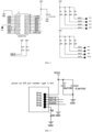
- FIG. 2 shows a circuit diagram of the present invention.
- the circuit diagram mainly shows a master control circuit.
- the master control circuit is a preferred implementation of the controller and its peripheral circuits.
- the master control circuit mainly adopts a chip MC32F7343 to control the circuits in the instruction reading building block 100 or other circuits in the instruction reading building block 100.
- the reading circuit is controlled in terms of the reading time, the reading sequence, the switch of the reading function, and so on.
- the prompt device which includes LED 1 to LED8 corresponding to eight plug-in positions of the instruction reading building block 100 shown in FIG. 1 , respectively, is controlled to prompt whether the instruction building block is plugged in to be electrically connected.
- the prompt device further includes Power _LED, which is controlled by the control circuit to indicate whether the instruction reading building block 100 has been powered on to be in a working state.
- the chip MC32F7343 provides a clock signal CLK_in and a data signal DAT_in.
- FIG. 3 shows an interface circuit of the master control circuit, wherein the interface circuit includes an interface CLK_in providing a clock signal and an interface DAT_in providing a data signal.
- the interface circuit is connected to other circuits or used as a test interface.
- the interface circuit is connected to the instruction circuit in the instruction building block 200 to realize the interfacing communication of the clock signal and the data signal.
- FIG. 4 shows another circuit diagram of the present invention, which can be interpreted as a variation of the circuit diagram shown in FIG. 2 .
- the relationship between the programming instructions contained in the plurality of instruction building blocks 200 is a parallel execution relationship.
- the relationship between the programming instructions contained in the plurality of instruction building blocks 200 is a serial execution relationship.
- the circuit diagram in FIG. 4 mainly shows the master control circuit.
- the master control circuit is a preferred implementation of the controller and its peripheral circuits.
- the master control circuit mainly adopts a chip MC35P7041.
- the chip MC35P7041 has clock signal pins CLK_in and CLK_out and further has data signal pins DAT_in and DAT_out.
- the chip MC35P7041 can control circuits in the instruction reading building block 100 or other circuits in the instruction reading building block 100.
- the reading circuit is controlled in terms of the reading time, the reading sequence, the switch of the reading function, and so on.
- the chip MC35P7041 provides the clock signal CLK_in and the data signal DAT_in.
- the circuit shown in FIG. 5 mainly adopts a chip MC3 5P7041.
- the circuit for example, can be applied to the instruction reading building block 100, and optionally, can also be applied to other building blocks.
- the circuit can output and/or receive command instructions.
- the command instruction is a data frame instruction mainly composed of data signals, or an instruction such as a pulse signal mainly composed of high-level and low-level signals, or transmits an optical signal instruction through an optocoupler peripheral circuit such as a light emitting diode or an infrared emitter.
- the instruction circuit is constructed according to actual needs.
- the instruction circuit is one or more components such as a resistor, capacitor, or transistor, to change the resistance or voltage drop.
- the instruction storage, instruction transmission, instruction receiving, instruction processing and the like in the instruction reading building block 100 are implemented by the corresponding chips. Further, those skilled in the art can add corresponding peripheral circuits according to actual needs, such as a current limiting protection circuit mainly composed of resistors, a communication circuit containing a wireless communication chip, and the like.
- the instruction reading building block 100 has a structure configured for assisting in triggering and indicating the command instructions, such as a piezoelectric circuit and a switch circuit.
Landscapes
- Engineering & Computer Science (AREA)
- Software Systems (AREA)
- General Engineering & Computer Science (AREA)
- Theoretical Computer Science (AREA)
- Physics & Mathematics (AREA)
- General Physics & Mathematics (AREA)
- Computer Security & Cryptography (AREA)
- Multimedia (AREA)
- Programmable Controllers (AREA)
- Instructional Devices (AREA)
- Toys (AREA)
- Circuit Arrangement For Electric Light Sources In General (AREA)
Description
- The present invention relates to the field of toy building blocks, and in particular to a programming building block.
- In the evolution of programming modes, the earliest mode for programming was to write codes directly in various programming languages, and later graphical programming was developed. Graphical programming uses the arrangement and nesting of graphic elements to form algorithmic logic, and generates the final code according to the algorithmic logic based on the code corresponding to each graphic.
- Graphical programming has been applied in the field of electronic building blocks, as being visually intuitive and easy to program. For example, graphical programming is performed on a tablet computer to obtain a control code, and then the control code is sent to a master control unit, which controls an execution unit to execute actions according to the control code. In this process, display devices such as tablet computers are essential for the need of graphical representation, but long-term programming will negatively affect the visual health of children and teenagers.
-
CN207694266U discloses a programmable building block toy including physicalinstruction building blocks 10, program recognition and compilingunit 20 and a program execution unit 30. However, the programmable building block toy does not allow complex programming. - In view of the shortcomings in the prior art, an objective of the present invention is to provide a programming building block.
- A programming building block provided according to the present invention includes an instruction
reading building block 100 and aninstruction building block 200. The instructionreading building block 100 includes an instruction readingbuilding block housing 101, a controller, and a reading circuit. The controller is located inside the instruction readingbuilding block housing 101 and electrically connected to the reading circuit. Reading areas of the reading circuit are located at a surface position of the instruction readingbuilding block housing 101. The controller reads an electrical signal at the reading areas to obtain reading signals, and outputs instruction signals according to the reading signals. - The
instruction building block 200 includes an instructionbuilding block housing 201 and an instruction circuit. To-be-read areas of the instruction circuit are located at a surface position of the instructionbuilding block housing 201. - The controller of the instruction
reading building block 100 reads the electrical signal of the instruction circuit of theinstruction building block 200 at the reading areas through coupling between the reading areas and the to-be-read areas. The coupling includes any one or more modes of electrical coupling, optical coupling, and magnetic coupling. One instruction reading building block can be read by another instruction reading building block, wherein the one instruction reading building block constitutes the instruction building block with respect to the another instruction reading building block. - Preferably,
the instructionreading building block 100 reads command instructions indicated by theinstruction building block 200. The command instructions include an instruction for setting a mode, an instruction for setting a behavior in the mode, and an instruction for setting a behavior or an upgrade instruction. A priority is set between the plurality of instructions for setting the mode. - A housing of the
instruction building block 200 is a splicing body, a card-like body or a plate-like body. - The command instructions are programs, data, circuit parameters or mechanical triggers.
- The programs are transmitted in a wired mode or a wireless mode, and the programs are stored in a volatile mode or a non-volatile mode.
- The circuit parameters include resistance, photosensitivity or piezoelectric parameters.
- Preferably, the instruction
reading building block 100 includes an output circuit, and the controller is connected to the output circuit.
An output area of the output circuit is located at a surface position of the instruction readingbuilding block housing 101, or the output area of the output circuit is located at an internal position of the instruction readingbuilding block housing 101. The controller outputs the instruction signals through the output area of the output circuit. - The output circuit adopts a wired output mode or a wireless output mode;
- At least one reading circuit and the output circuit are an identical circuit, or the reading circuit and the output circuit are different circuits.
- The instruction reading building block includes a switch unit. After the instruction building block is plugged in, the switch unit is triggered, and the instruction reading building block reads the electrical signal at the reading areas.
- Preferably, the controller determines an output time sequence of the instruction signals corresponding to the plurality of reading areas according to a positional relationship or a logical relationship between the plurality of reading areas.
- Preferably, at least one instruction information is obtained by the controller according to the plurality of reading signals.
- Preferably, the plurality of reading signals are read from one reading area or from one or more reading areas.
- Preferably, at least one read information is configured for indicating the output time sequence of the instruction signals.
- Preferably, the electrical coupling adopts a wired mode, the reading areas and the to-be-read areas are matched connectors, and the reading circuit is wired to the instruction circuit when the reading areas are mated with the to-be-read areas.
- Preferably, the electrical coupling adopts a wireless mode, the reading areas and the to-be-read areas constitute a signal transmission channel, and the reading circuit reads the electrical signal emitted by the instruction circuit through the signal transmission channel.
- Preferably, the instruction
reading building block 100 includes a prompt device. - The prompt device indicates a coupling state between the reading areas and the to-be-read areas.
- The instruction
building block housing 201 includes a light observation channel. - When the electrical coupling is formed between the reading areas and the to-be-read areas, light emitted by the prompt device can exit through the light observation channel.
- Preferably,
the reading area of the reading circuit includes at least one set of first-type circuit contact connectors. - The to-be-read area of the instruction circuit includes at least one set of second-type circuit contact connectors.
- The instruction reading
building block housing 101 includes at least one set of first-type building block connectors. - The instruction
building block housing 201 includes at least one set of second-type building block connectors. - When the first-type building block connectors are adaptively connected to the second-type building block connectors, the first-type circuit contact connectors are adaptively connected to the second-type circuit contact connectors to form a conductive path.
- Preferably,
- one or more sets of first-type circuit contact connectors are correspondingly and fixedly provided on a set of first-type building block connectors; and
- one or more sets of second-type circuit contact connectors are correspondingly and fixedly provided on a set of second-type building block connectors.
- Preferably,
- the first-type circuit contact connector includes a power connector and/or a signal interface; and
- the second-type circuit contact connector includes a power connector and/or a signal interface.
- Preferably, when the electrical coupling is formed between the reading areas and the to-be-read areas, a plurality of first-type circuit contact connectors in the same set are connected through the corresponding set of second-type circuit contact connectors to form a loop, and the loop is further connected to the controller and the instruction circuit.
- The controller reads circuit parameters of the instruction circuit as the reading signals through the loop.
- Preferably, a physical parameter sequence of a plurality of sets of first-type building block connectors corresponding to the reading areas indicates a reading sequence or an execution sequence of the instruction signals.
- The physical parameter sequence is configured in the controller, or the physical parameter sequence is indicated to the controller through a signal parameter sequence generated by an adjusting circuit.
- The signal parameter sequence generated by the adjusting circuit includes:
- a time sequence generated by a delay circuit; or
- a sequence of an amplitude magnitude, a frequency magnitude or a phase magnitude caused by a modulator.
- Preferably, the controller includes a master control circuit, and the master control circuit mainly adopts a chip MC32F7343.
- The master control circuit performs control on the reading circuit, and the control includes a reading time, a reading sequence, and a switch of a reading function.
- The master control circuit controls the prompt device. The prompt device includes a plurality of position indicator lights LED corresponding to a plurality of plug-in positions of the
instruction building block 100, respectively, and prompts whether the instruction building block is plugged to be electrically connected. The prompt device further includes a power indicator Power_LED, which is controlled by the control circuit to indicate whether the instruction readingbuilding block 100 has been powered on to be in a working state. - The master control circuit provides a clock signal and a data signal.
- Preferably, the instruction circuit in the instruction building block is configured for outputting command instructions. The command instruction is a data frame instruction mainly composed of data signals, or an instruction such as a pulse signal mainly composed of high-level and low-level signals, or transmits an optical signal instruction through an optocoupler peripheral circuit such as a light emitting diode or an infrared emitter.
- Preferably, the instruction circuit is one or more discrete components, and is configured to change the resistance or voltage drop of the loop after being connected to the loop.
- Preferably, the reading circuit has a clock signal pin and further has a data signal pin or a voltage signal pin. Through the data signal pin, data from the instruction circuit are obtained to obtain the command instructions. A change in the voltage value after the instruction circuit is connected is obtained through the voltage signal pin.
- Preferably, the instruction reading
building block 100 has a structure configured for assisting in triggering and indicating the command instructions, including a piezoelectric circuit or a switching circuit. - Compared with the prior art, the present invention has the following advantages. Programming can be performed without an electronic display device.
- Other features, objectives and advantages of the present invention will become more apparent from reading the detailed description of non-restrictive embodiments with reference to the drawings.
-
FIG. 1 is a structural schematic diagram of the present invention; -
FIG. 2 is a circuit diagram of a master control circuit containing a controller suitable for parallel programming in an instructionreading building block 100; -
FIG. 3 shows an interface circuit of the master control circuit containing a reading circuit suitable for parallel programming in the instruction readingbuilding block 100; -
FIG. 4 is a circuit diagram of the master control circuit suitable for serial programming, where the circuit can be applied to the instruction readingbuilding block 100 in a preferred embodiment, and optionally, can also be applied to other building blocks; and -
FIG. 5 shows a circuit diagram and interface circuit of a serial plug-in programming module, where the circuit can be applied to the instruction readingbuilding block 100 in a preferred embodiment, and optionally, can also be applied to other building blocks. - The present invention is described in detail below in conjunction with the specific embodiments. The following embodiments help those skilled in the art further understand the present invention, but do not limit the present invention in any form. It should be noted that those ordinarily skilled in the art can make several changes and modifications without departing from the concept of the present invention. These changes and modifications shall fall within the scope of protection of the present invention.
- A programming building block provided according to the present invention includes the instruction reading
building block 100 and theinstruction building block 200. - The instruction
reading building block 100 is a connection building block, reads an instruction from theinstruction building block 200 and outputs the instruction to other building blocks, such as a master control building block or an execution building block. The instructionreading building block 100 itself can be the master control building block or the execution building block. - When reading a plurality of instructions from a plurality of
instruction building blocks 200, the master control building block executes these instructions sequentially, or obtains a new instruction according to operations of the plurality of instructions and then executes the new instruction. - One instruction
reading building block 100 can be read by another instruction readingbuilding block 100, wherein the one instructionreading building block 100 constitutes theinstruction building block 200 with respect to the another instruction readingbuilding block 100. - The instruction
reading building block 100 reads command instructions indicated by theinstruction building block 200. The command instructions include an instruction for setting a mode, an instruction for setting a behavior in the mode, an instruction for setting a behavior or an upgrade instruction. A priority is set between the plurality of instructions for setting the mode. - The command instructions are stored in the
instruction building block 200 in advance, or generated by theinstruction building block 200 in real time, or the instruction building block triggers the instruction readingbuilding block 100 to obtain the instructions stored locally, or the instruction building block triggers the instruction readingbuilding block 100 to generate the instructions locally in real time. - The mode is a master control building block mode or an instruction reading building block mode. For example, the instruction reading building block has different instruction reading sequences or instruction output sequences in different modes.
- For example, one mode is a stop mode that has the highest priority.
- Instructions of the same behavior indicate an execution unit to execute different behaviors in different modes.
- The housing of the
instruction building block 200 is a splicing body, a card-like body or a plate-like body. - The
instruction building blocks 200 are connected in series, in parallel or in series and parallel. - The
instruction building blocks 200 can be plugged in and stacked to each other. The splicing bodies can be plugged in and connected to each other. - The card-like body is, for example, a card.
- The plate-like body is, for example, a programming board.
- The command instructions are programs, data, circuit parameters or mechanical triggers.
- The programs are transmitted in a wired mode and a wireless mode. The programs are stored in a volatile mode or a non-volatile mode.
- The circuit parameters include resistance, photosensitivity or piezoelectric parameters.
- The instruction
reading building block 100 includes the instruction readingbuilding block housing 101, a controller, and a reading circuit. The controller is located inside the instruction readingbuilding block housing 101 and electrically connected to the reading circuit. Reading areas of the reading circuit are located at a surface position of the instruction readingbuilding block housing 101. The controller reads an electrical signal at the reading areas to obtain reading signals, and outputs instruction signals according to the reading signals. - The
instruction building block 200 includes the instructionbuilding block housing 201 and an instruction circuit. To-be-read areas of the instruction circuit are located at a surface position of the instructionbuilding block housing 201. The controller of the instruction readingbuilding block 100 reads the electrical signal of the instruction circuit of theinstruction building block 200 at the reading areas through the coupling between the reading areas and the to-be-read areas. The coupling includes any one or more modes of electrical coupling, optical coupling, and magnetic coupling. Preferably, the instruction readingbuilding block 100 includes an output circuit. The controller is connected to the output circuit. An output area of the output circuit is located at a surface position of the instruction readingbuilding block housing 101, or the output area of the output circuit is located at an internal position of the instruction readingbuilding block housing 101. The controller outputs the instruction signals through the output area of the output circuit. - The output circuit adopts a wired output mode or a wireless output mode. At least one reading circuit and the output circuit are an identical circuit, or the reading circuit and the output circuit are different circuits. The instruction reading building block includes a switch unit. After the instruction building block is plugged in, the switch unit is triggered, and the instruction reading building block reads the electrical signal at the reading areas. The controller determines an output time sequence of the instruction signals corresponding to the plurality of reading areas according to a positional relationship or a logical relationship between the plurality of reading areas. At least one instruction information is obtained by the controller according to one or more reading signals. The plurality of reading signals are read from one reading area or from a plurality of reading areas. At least one read information is configured for indicating the output time sequence of the instruction signals. When the electrical coupling adopts a wired mode, the reading areas and the to-be-read areas are matched connectors, and the reading circuit is wired to the instruction circuit when the reading areas are mated with the to-be-read areas. When the electrical coupling adopts a wireless mode, the reading areas and the to-be-read areas constitute a signal transmission channel, and the reading circuit reads the electrical signal emitted by the instruction circuit through the signal transmission channel.
- The instruction
reading building block 100 includes a prompt device. The prompt device indicates a coupling state between the reading areas and the to-be-read areas. The instructionbuilding block housing 201 includes a light observation channel. When the electrical coupling is formed between the reading areas and the to-be-read areas, light emitted by the prompt device can exit through the light observation channel. - The reading area of the reading circuit includes at least one set of first-type circuit contact connectors.
- The to-be-read area of the instruction circuit includes at least one set of second-type circuit contact connectors.
- The instruction reading
building block housing 101 includes at least one set of first-type building block connectors. - The instruction
building block housing 201 includes at least one set of second-type building block connectors. - When the first-type building block connectors are adaptively connected to the second-type building block connectors, the first-type circuit contact connectors are adaptively connected to the second-type circuit contact connectors to form a conductive path.
- One or more sets of first-type circuit contact connectors are correspondingly and fixedly provided on a set of first-type building block connectors.
- One or more sets of second-type circuit contact connectors are correspondingly and fixedly provided on a set of second-type building block connectors.
- The first-type circuit contact connector includes a power connector and/or a signal interface.
- The second-type circuit contact connector includes a power connector and/or a signal interface.
- Preferably, when the electrical coupling is formed between the reading areas and the to-be-read areas, a plurality of first-type circuit contact connectors in the same set are connected through the corresponding set of second-type circuit contact connectors to form a loop, and the loop is further connected to the controller and the instruction circuit. The controller reads circuit parameters of the instruction circuit as the reading signals through the loop. A physical parameter sequence of a plurality of sets of first-type building block connectors corresponding to the reading areas indicates a reading sequence or an execution sequence of the instruction signals. The physical parameter sequence is configured in the controller, or the physical parameter sequence is indicated to the controller through a signal parameter sequence generated by an adjusting circuit. The signal parameter sequence generated by the adjusting circuit includes: a time sequence generated by a delay circuit, or the sequence of an amplitude magnitude, a frequency magnitude or a phase magnitude caused by a modulator.
- TP1 to TP 16 in the figures are test points, or correspond to or are connected to a circuit contact connector in a preferred or variant example. When the instruction building block and the instruction reading building block are plugged in, chips, resistors, transistors and other components in the figures are connected through the corresponding TP terminals.
-
FIG. 2 shows a circuit diagram of the present invention. The circuit diagram mainly shows a master control circuit. The master control circuit is a preferred implementation of the controller and its peripheral circuits. The master control circuit mainly adopts a chip MC32F7343 to control the circuits in the instruction readingbuilding block 100 or other circuits in the instruction readingbuilding block 100. For example, the reading circuit is controlled in terms of the reading time, the reading sequence, the switch of the reading function, and so on. For another example, the prompt device, which includesLED 1 to LED8 corresponding to eight plug-in positions of the instruction readingbuilding block 100 shown inFIG. 1 , respectively, is controlled to prompt whether the instruction building block is plugged in to be electrically connected. The prompt device further includes Power _LED, which is controlled by the control circuit to indicate whether the instruction readingbuilding block 100 has been powered on to be in a working state. In addition, the chip MC32F7343 provides a clock signal CLK_in and a data signal DAT_in. -
FIG. 3 shows an interface circuit of the master control circuit, wherein the interface circuit includes an interface CLK_in providing a clock signal and an interface DAT_in providing a data signal. The interface circuit is connected to other circuits or used as a test interface. For example, the interface circuit is connected to the instruction circuit in theinstruction building block 200 to realize the interfacing communication of the clock signal and the data signal. -
FIG. 4 shows another circuit diagram of the present invention, which can be interpreted as a variation of the circuit diagram shown inFIG. 2 . InFIG. 2 , the relationship between the programming instructions contained in the plurality ofinstruction building blocks 200 is a parallel execution relationship. InFIG. 4 , the relationship between the programming instructions contained in the plurality ofinstruction building blocks 200 is a serial execution relationship. - The circuit diagram in
FIG. 4 mainly shows the master control circuit. The master control circuit is a preferred implementation of the controller and its peripheral circuits. The master control circuit mainly adopts a chip MC35P7041. The chip MC35P7041 has clock signal pins CLK_in and CLK_out and further has data signal pins DAT_in and DAT_out. The chip MC35P7041 can control circuits in the instruction readingbuilding block 100 or other circuits in the instruction readingbuilding block 100. For example, the reading circuit is controlled in terms of the reading time, the reading sequence, the switch of the reading function, and so on. In addition, the chip MC35P7041 provides the clock signal CLK_in and the data signal DAT_in. - The circuit shown in
FIG. 5 mainly adopts a chip MC3 5P7041. The circuit, for example, can be applied to the instruction readingbuilding block 100, and optionally, can also be applied to other building blocks. With the chip MC35P7041, the circuit can output and/or receive command instructions. The command instruction is a data frame instruction mainly composed of data signals, or an instruction such as a pulse signal mainly composed of high-level and low-level signals, or transmits an optical signal instruction through an optocoupler peripheral circuit such as a light emitting diode or an infrared emitter. - The instruction circuit is constructed according to actual needs. For example, the instruction circuit is one or more components such as a resistor, capacitor, or transistor, to change the resistance or voltage drop.
- Through the illustration of the above circuit diagrams, the instruction storage, instruction transmission, instruction receiving, instruction processing and the like in the instruction reading
building block 100 are implemented by the corresponding chips. Further, those skilled in the art can add corresponding peripheral circuits according to actual needs, such as a current limiting protection circuit mainly composed of resistors, a communication circuit containing a wireless communication chip, and the like. - Those skilled in the art can implement the peripheral circuits of each chip in the above circuit diagrams according to actual needs with reference to the datasheet of the chip, which will not be repeated herein.
- Further, when the
instruction building block 200 triggers and indicates the command instructions mechanically, there may be no circuit in theinstruction building block 200. Accordingly, the instruction readingbuilding block 100 has a structure configured for assisting in triggering and indicating the command instructions, such as a piezoelectric circuit and a switch circuit. - The specific embodiments of the present invention have been described above. It should be understood that the present invention is not limited to the above particular embodiments and that various changes or modifications can be made by those skilled in the art within the scope of the claims without affecting the substantial contents of the present invention. Embodiments and features in the embodiments of the present invention can be arbitrarily combined with each other when not in conflict.
Claims (14)
- A programming building block, comprisingan instruction reading building block (100) and an instruction building block (200), whereinthe instruction reading building block (100) comprises an instruction reading building block housing (101), a controller, and a reading circuit;the controller is located inside the instruction reading building block housing (101) and the controller is electrically connected to the reading circuit;a plurality of reading areas of the reading circuit are located at a first surface position of the instruction reading building block housing (101);the controller reads an electrical signal at the plurality of reading areas to obtain reading signals, and the controller outputs instruction signals according to the reading signals;the instruction building block (200) comprises an instruction building block housing (201) and an instruction circuit;
a plurality of to-be-read areas of the instruction circuit are located at a surface position of the instruction building block housing (201); andthe controller of the instruction reading building block (100) reads the electrical signal of the instruction building block (200) at the plurality of reading areas through a coupling between the plurality of reading areas and the plurality of to-be-read areas, wherein the coupling comprises at least one of electrical coupling, optical coupling, and magnetic coupling, and characterized in thatone instruction reading building block (100) can be read by another instruction reading building block (100), wherein the one instruction reading building block (100) constitutes the instruction building block (200) with respect to the another instruction reading building block (100). - The programming building block as claimed in claim 1, whereinthe instruction reading building block (100) reads command instructions indicated by the instruction building block (200), and the command instructions comprise a plurality of instructions for setting a first mode, an instruction for setting a first behavior in a second mode, an instruction for setting a second behavior, or an upgrade instruction;a priority is set between the plurality of instructions for setting the first mode;a housing of the instruction building block (200) is a splicing body, a card-like body or a plate-like body;the command instructions are programs, data, circuit parameters or mechanical triggers;the programs are transmitted in a wired mode or a wireless mode;the programs are stored in a volatile mode or a non-volatile mode; andthe circuit parameters comprise resistance parameters, photosensitivity parameters or piezoelectric parameters.
- The programming building block as claimed in claim 1, whereinthe instruction reading building block (100) comprises an output circuit;the controller is connected to the output circuit;an output area of the output circuit is located at a second surface position of the instruction reading building block housing (101), or the output area of the output circuit is located at an internal position of the instruction reading building block housing (101);the controller outputs the instruction signals through the output area of the output circuit;the output circuit adopts a wired output mode or a wireless output mode;at least one reading circuit and the output circuit are an identical circuit, or the reading circuit and the output circuit are different circuits;the instruction reading building block comprises a switch unit, andafter the instruction building block is plugged in, the switch unit is triggered, and the instruction reading building block reads the electrical signal at the plurality of reading areas.
- The programming building block as claimed in claim 1, wherein
the controller determines an output time sequence of the instruction signals corresponding to the plurality of reading areas according to a positional relationship or a logical relationship between the plurality of reading areas. - The programming building block as claimed in claim 1, wherein
at least one instruction information is obtained by the controller according to the reading signals. - The programming building block as claimed in claim 5, wherein
the reading signals are read from at least one of the plurality of reading areas. - The programming building block as claimed in claim 1, wherein
at least one read information is configured for indicating an output time sequence of instruction signals. - The programming building block as claimed in claim 1, whereinthe electrical coupling adopts a wired mode, the plurality of reading areas and the plurality of to-be-read areas are matched connectors; and the reading circuit is wired to the instruction circuit when the plurality of reading areas are mated with the plurality of to-be-read areas; orthe electrical coupling adopts a wireless mode, the plurality of reading areas and the plurality of to-be-read areas constitute a signal transmission channel, and the reading circuit reads the electrical signal emitted by the instruction circuit through the signal transmission channel.
- The programming building block as claimed in claim 1, whereinthe instruction reading building block (100) comprises a prompt device;the prompt device indicates a coupling state between the plurality of reading areas and the plurality of to-be-read areas;the instruction building block housing (201) comprises a light observation channel; andwhen the electrical coupling is formed between the plurality of reading areas and the plurality of to-be-read areas, a light emitted by the prompt device exits through the light observation channel.
- The programming building block as claimed in claim 1, whereineach of the plurality of reading areas of the reading circuit comprises at least one set of first-type circuit contact connectors;each of the plurality of to-be-read areas of the instruction circuit comprises at least one set of second-type circuit contact connectors;the instruction reading building block housing (101) comprises at least one set of first-type building block connectors;the instruction building block housing (201) comprises at least one set of second-type building block connectors; andwhen the at least one set of first-type building block connectors are adaptively connected to the at least one set of second-type building block connectors, the at least one set of first-type circuit contact connectors are adaptively connected to the at least one set of second-type circuit contact connectors to form a conductive path.
- The programming building block as claimed in claim 10, whereinthe at least one set of first-type circuit contact connectors are correspondingly and fixedly provided on the at least one set of first-type building block connectors; andthe at least one set of second-type circuit contact connectors are correspondingly and fixedly provided on the at least one set of second-type building block connectors.
- The programming building block as claimed in claim 10, whereineach of the at least one set of first-type circuit contact connectors comprises a first power connector and/or a first signal interface; andeach of the at least one set of second-type circuit contact connectors comprises a second power connector and/or a second signal interface.
- The programming building block as claimed in claim 10, whereinwhen the electrical coupling is formed between the plurality of reading areas and the plurality of to-be-read areas, the at least one set of first-type circuit contact connectors are connected through the at least one set of second-type circuit contact connectors to form a loop, and the loop is further connected to the controller and the instruction circuit; andthe controller reads circuit parameters of the instruction circuit as the reading signals through the loop.
- The programming building block as claimed in claim 1, whereina physical parameter sequence of the at least one set of first-type building block connectors corresponding to the plurality of reading areas indicates a reading sequence or an execution sequence of the instruction signals;the physical parameter sequence is configured in the controller, or the physical parameter sequence is indicated to the controller through a signal parameter sequence generated by an adjusting circuit; andthe signal parameter sequence generated by the adjusting circuit comprises:a time sequence generated by a delay circuit; ora sequence of an amplitude magnitude, a frequency magnitude or a phase magnitude, wherein the amplitude magnitude, the frequency magnitude or the phase magnitude are caused by a modulator.
Applications Claiming Priority (2)
| Application Number | Priority Date | Filing Date | Title |
|---|---|---|---|
| CN201811572649.5A CN111346390B (en) | 2018-12-21 | 2018-12-21 | Programming building block |
| PCT/CN2019/122309 WO2020125385A1 (en) | 2018-12-21 | 2019-12-02 | Programming building block |
Publications (4)
| Publication Number | Publication Date |
|---|---|
| EP3900802A1 EP3900802A1 (en) | 2021-10-27 |
| EP3900802A4 EP3900802A4 (en) | 2022-03-09 |
| EP3900802C0 EP3900802C0 (en) | 2023-06-07 |
| EP3900802B1 true EP3900802B1 (en) | 2023-06-07 |
Family
ID=71102465
Family Applications (1)
| Application Number | Title | Priority Date | Filing Date |
|---|---|---|---|
| EP19898291.0A Active EP3900802B1 (en) | 2018-12-21 | 2019-12-02 | Programming building block |
Country Status (6)
| Country | Link |
|---|---|
| US (1) | US12076659B2 (en) |
| EP (1) | EP3900802B1 (en) |
| JP (1) | JP7358477B2 (en) |
| KR (1) | KR102676572B1 (en) |
| CN (1) | CN111346390B (en) |
| WO (1) | WO2020125385A1 (en) |
Families Citing this family (3)
| Publication number | Priority date | Publication date | Assignee | Title |
|---|---|---|---|---|
| US20220001292A1 (en) * | 2020-06-18 | 2022-01-06 | Saifeng Chen | Programmable toy building blocks system |
| CN112130844A (en) * | 2020-07-31 | 2020-12-25 | 北京编程猫科技有限公司 | Method and device for adding physical parameters based on imaging programming platform |
| CN116954122A (en) * | 2023-07-27 | 2023-10-27 | 上海鲸鱼机器人科技有限公司 | A programming device and method based on serial identification code instructions |
Family Cites Families (23)
| Publication number | Priority date | Publication date | Assignee | Title |
|---|---|---|---|---|
| US7316567B2 (en) * | 2003-08-01 | 2008-01-08 | Jennifer Chia-Jen Hsieh | Physical programming toy |
| US7556563B2 (en) * | 2005-01-10 | 2009-07-07 | Mattel, Inc. | Internet enabled multiply interconnectable environmentally interactive character simulation module method and system |
| GB201019285D0 (en) * | 2010-11-15 | 2010-12-29 | Hepworth Browne Ltd | Interactive system and method of modifying user interaction therein |
| EP3042704B1 (en) * | 2011-05-23 | 2019-03-06 | Lego A/S | A toy construction system |
| WO2013017138A1 (en) * | 2011-07-29 | 2013-02-07 | Deutsche Telekom Ag | Construction toy comprising a plurality of interconnectable building elements, set of a plurality of interconnectable building elements, and method to control and/or monitor a construction toy |
| JP6324716B2 (en) * | 2013-12-26 | 2018-05-16 | 株式会社ソニー・インタラクティブエンタテインメント | Block, block system, display method, and information processing method |
| EP3142094A4 (en) | 2014-05-07 | 2017-04-26 | Jin Wook Kim | Algorithm teaching apparatus using blocks |
| CA3275029A1 (en) | 2014-05-15 | 2025-10-30 | Lego A/S | A toy construction system with function construction elements |
| WO2017014530A1 (en) * | 2015-07-20 | 2017-01-26 | 이준희 | Block toy having topology recognition function and content providing system using same |
| CN105435468A (en) * | 2015-12-11 | 2016-03-30 | 北京爱其科技有限公司 | Toy building method and built toy |
| JP6176870B2 (en) | 2016-01-05 | 2017-08-09 | 株式会社セガ トイズ | Coding toy, block, stage, figurine toy and coding method |
| CN106139614A (en) | 2016-07-22 | 2016-11-23 | 苏州乐派特机器人有限公司 | A kind of method for gaming utilizing material objectization programming operation to carry out |
| US10304353B1 (en) * | 2016-08-15 | 2019-05-28 | Delfin Lozano | Tray-and-block apparatus for device programming |
| CN107065604A (en) * | 2017-01-12 | 2017-08-18 | 苏州乐派特机器人有限公司 | A kind of programmable object wearing device |
| CN106924977A (en) * | 2017-02-28 | 2017-07-07 | 腾讯科技(深圳)有限公司 | Modular system, topology identification method, apparatus and system |
| JP6877688B2 (en) * | 2017-03-27 | 2021-05-26 | カシオ計算機株式会社 | Programming device and its control program, programming method |
| KR20180133162A (en) * | 2017-06-05 | 2018-12-13 | 신재광 | STRUCTURE FOR ASSEMBLING OF MODULAR ROBOTICS SYSTEM BASED ON IoT |
| CN207233254U (en) * | 2017-07-05 | 2018-04-13 | 南京阿凡达机器人科技有限公司 | A kind of building block system programming device |
| US10890897B2 (en) * | 2017-09-26 | 2021-01-12 | International Business Machines Corporation | Assembly of a modular structure |
| CN207694266U (en) * | 2017-12-25 | 2018-08-07 | 广东洪恩教育科技有限公司 | A programmable building block toy |
| CN108310781B (en) * | 2018-03-08 | 2023-12-29 | 广州途道信息科技有限公司 | Hierarchical electronic building block, self-programming method and building block assembly |
| CN108525325A (en) * | 2018-04-24 | 2018-09-14 | 深圳小西科技有限公司 | A kind of building block system instruction module, host apparatus and modular system |
| CN108766118B (en) * | 2018-08-24 | 2023-08-25 | 杭州高低科技有限公司 | Tangible programming building block easy for programming education |
-
2018
- 2018-12-21 CN CN201811572649.5A patent/CN111346390B/en active Active
-
2019
- 2019-12-02 WO PCT/CN2019/122309 patent/WO2020125385A1/en not_active Ceased
- 2019-12-02 EP EP19898291.0A patent/EP3900802B1/en active Active
- 2019-12-02 US US17/417,095 patent/US12076659B2/en active Active
- 2019-12-02 KR KR1020217020440A patent/KR102676572B1/en active Active
- 2019-12-02 JP JP2021536013A patent/JP7358477B2/en active Active
Also Published As
| Publication number | Publication date |
|---|---|
| EP3900802C0 (en) | 2023-06-07 |
| WO2020125385A1 (en) | 2020-06-25 |
| EP3900802A4 (en) | 2022-03-09 |
| JP7358477B2 (en) | 2023-10-10 |
| JP2022515191A (en) | 2022-02-17 |
| US20220072441A1 (en) | 2022-03-10 |
| US12076659B2 (en) | 2024-09-03 |
| CN111346390A (en) | 2020-06-30 |
| KR102676572B1 (en) | 2024-06-18 |
| CN111346390B (en) | 2020-12-25 |
| EP3900802A1 (en) | 2021-10-27 |
| KR20210097177A (en) | 2021-08-06 |
Similar Documents
| Publication | Publication Date | Title |
|---|---|---|
| US12076659B2 (en) | Programming building block | |
| CN101433465B (en) | Ultrasonic instrument and multiple-probe control method thereof | |
| US11919162B2 (en) | ID number setting method, computer-readable storage medium and modular device | |
| JP2004326342A (en) | Modular computer system and I / O module | |
| US11901668B2 (en) | Modular device, control method and robot | |
| CN109509422A (en) | display panel drive circuit and display device | |
| US10456910B2 (en) | Educational systems comprising programmable controllers and methods of teaching therewith | |
| CN112775977B (en) | Programming device and method for controlling based on resistance | |
| CN116073152B (en) | Board transfer equipment and test method, system, device, equipment and storage medium | |
| CN108508812B (en) | AGV controller IO port multiplexing configuration system and method | |
| US20150347348A1 (en) | Smart connector for electronic components | |
| KR101622521B1 (en) | Programmable Logic Controller Communication Device | |
| US11050461B2 (en) | Toy, method for controlling a toy, and computer program product | |
| CN109683593A (en) | A kind of impulse type servo-driver Basic function testing method and apparatus | |
| CN119576850A (en) | An FPGA accelerator card with hard synchronization function | |
| RU119141U1 (en) | PROGRAMMER OF TELEVISION MEMORY ICs | |
| CN211857727U (en) | Test equipment for simulating remote controller | |
| CN207867280U (en) | The electronic building brick and sensor of programmable study | |
| CN109979405B (en) | Time sequence control circuit and display device | |
| CN222441687U (en) | Level conversion circuit and electronic equipment | |
| US6215418B1 (en) | Programmable membrane switch input/output system | |
| CN109960180B (en) | Programmable learning electronics and sensors | |
| CN112859765A (en) | AGV capable of flexibly configuring instructions | |
| CN214505005U (en) | Application verification circuit for memory device | |
| CN110908315B (en) | An industrial electronic lock |
Legal Events
| Date | Code | Title | Description |
|---|---|---|---|
| STAA | Information on the status of an ep patent application or granted ep patent |
Free format text: STATUS: THE INTERNATIONAL PUBLICATION HAS BEEN MADE |
|
| PUAI | Public reference made under article 153(3) epc to a published international application that has entered the european phase |
Free format text: ORIGINAL CODE: 0009012 |
|
| STAA | Information on the status of an ep patent application or granted ep patent |
Free format text: STATUS: REQUEST FOR EXAMINATION WAS MADE |
|
| 17P | Request for examination filed |
Effective date: 20210720 |
|
| AK | Designated contracting states |
Kind code of ref document: A1 Designated state(s): AL AT BE BG CH CY CZ DE DK EE ES FI FR GB GR HR HU IE IS IT LI LT LU LV MC MK MT NL NO PL PT RO RS SE SI SK SM TR |
|
| A4 | Supplementary search report drawn up and despatched |
Effective date: 20220204 |
|
| RIC1 | Information provided on ipc code assigned before grant |
Ipc: A63H 33/04 20060101AFI20220131BHEP |
|
| DAV | Request for validation of the european patent (deleted) | ||
| DAX | Request for extension of the european patent (deleted) | ||
| GRAP | Despatch of communication of intention to grant a patent |
Free format text: ORIGINAL CODE: EPIDOSNIGR1 |
|
| STAA | Information on the status of an ep patent application or granted ep patent |
Free format text: STATUS: GRANT OF PATENT IS INTENDED |
|
| INTG | Intention to grant announced |
Effective date: 20221104 |
|
| RIN1 | Information on inventor provided before grant (corrected) |
Inventor name: LIU, CHENLU Inventor name: LIU, SONG Inventor name: ZHAO, JIALIANG Inventor name: GAO, CHAO Inventor name: SHU, QINMAO Inventor name: XIAO, YE Inventor name: LI, BIN |
|
| GRAS | Grant fee paid |
Free format text: ORIGINAL CODE: EPIDOSNIGR3 |
|
| GRAA | (expected) grant |
Free format text: ORIGINAL CODE: 0009210 |
|
| STAA | Information on the status of an ep patent application or granted ep patent |
Free format text: STATUS: THE PATENT HAS BEEN GRANTED |
|
| AK | Designated contracting states |
Kind code of ref document: B1 Designated state(s): AL AT BE BG CH CY CZ DE DK EE ES FI FR GB GR HR HU IE IS IT LI LT LU LV MC MK MT NL NO PL PT RO RS SE SI SK SM TR |
|
| REG | Reference to a national code |
Ref country code: GB Ref legal event code: FG4D |
|
| REG | Reference to a national code |
Ref country code: CH Ref legal event code: EP Ref country code: AT Ref legal event code: REF Ref document number: 1573224 Country of ref document: AT Kind code of ref document: T Effective date: 20230615 |
|
| REG | Reference to a national code |
Ref country code: DE Ref legal event code: R096 Ref document number: 602019030819 Country of ref document: DE |
|
| U01 | Request for unitary effect filed |
Effective date: 20230704 |
|
| U07 | Unitary effect registered |
Designated state(s): AT BE BG DE DK EE FI FR IT LT LU LV MT NL PT SE SI Effective date: 20230727 |
|
| REG | Reference to a national code |
Ref country code: LT Ref legal event code: MG9D |
|
| PG25 | Lapsed in a contracting state [announced via postgrant information from national office to epo] |
Ref country code: NO Free format text: LAPSE BECAUSE OF FAILURE TO SUBMIT A TRANSLATION OF THE DESCRIPTION OR TO PAY THE FEE WITHIN THE PRESCRIBED TIME-LIMIT Effective date: 20230907 Ref country code: ES Free format text: LAPSE BECAUSE OF FAILURE TO SUBMIT A TRANSLATION OF THE DESCRIPTION OR TO PAY THE FEE WITHIN THE PRESCRIBED TIME-LIMIT Effective date: 20230607 |
|
| PG25 | Lapsed in a contracting state [announced via postgrant information from national office to epo] |
Ref country code: RS Free format text: LAPSE BECAUSE OF FAILURE TO SUBMIT A TRANSLATION OF THE DESCRIPTION OR TO PAY THE FEE WITHIN THE PRESCRIBED TIME-LIMIT Effective date: 20230607 Ref country code: HR Free format text: LAPSE BECAUSE OF FAILURE TO SUBMIT A TRANSLATION OF THE DESCRIPTION OR TO PAY THE FEE WITHIN THE PRESCRIBED TIME-LIMIT Effective date: 20230607 Ref country code: GR Free format text: LAPSE BECAUSE OF FAILURE TO SUBMIT A TRANSLATION OF THE DESCRIPTION OR TO PAY THE FEE WITHIN THE PRESCRIBED TIME-LIMIT Effective date: 20230908 |
|
| PG25 | Lapsed in a contracting state [announced via postgrant information from national office to epo] |
Ref country code: SK Free format text: LAPSE BECAUSE OF FAILURE TO SUBMIT A TRANSLATION OF THE DESCRIPTION OR TO PAY THE FEE WITHIN THE PRESCRIBED TIME-LIMIT Effective date: 20230607 |
|
| PG25 | Lapsed in a contracting state [announced via postgrant information from national office to epo] |
Ref country code: IS Free format text: LAPSE BECAUSE OF FAILURE TO SUBMIT A TRANSLATION OF THE DESCRIPTION OR TO PAY THE FEE WITHIN THE PRESCRIBED TIME-LIMIT Effective date: 20231007 |
|
| PG25 | Lapsed in a contracting state [announced via postgrant information from national office to epo] |
Ref country code: SM Free format text: LAPSE BECAUSE OF FAILURE TO SUBMIT A TRANSLATION OF THE DESCRIPTION OR TO PAY THE FEE WITHIN THE PRESCRIBED TIME-LIMIT Effective date: 20230607 Ref country code: SK Free format text: LAPSE BECAUSE OF FAILURE TO SUBMIT A TRANSLATION OF THE DESCRIPTION OR TO PAY THE FEE WITHIN THE PRESCRIBED TIME-LIMIT Effective date: 20230607 Ref country code: RO Free format text: LAPSE BECAUSE OF FAILURE TO SUBMIT A TRANSLATION OF THE DESCRIPTION OR TO PAY THE FEE WITHIN THE PRESCRIBED TIME-LIMIT Effective date: 20230607 Ref country code: IS Free format text: LAPSE BECAUSE OF FAILURE TO SUBMIT A TRANSLATION OF THE DESCRIPTION OR TO PAY THE FEE WITHIN THE PRESCRIBED TIME-LIMIT Effective date: 20231007 Ref country code: CZ Free format text: LAPSE BECAUSE OF FAILURE TO SUBMIT A TRANSLATION OF THE DESCRIPTION OR TO PAY THE FEE WITHIN THE PRESCRIBED TIME-LIMIT Effective date: 20230607 |
|
| U20 | Renewal fee for the european patent with unitary effect paid |
Year of fee payment: 5 Effective date: 20231228 |
|
| PG25 | Lapsed in a contracting state [announced via postgrant information from national office to epo] |
Ref country code: PL Free format text: LAPSE BECAUSE OF FAILURE TO SUBMIT A TRANSLATION OF THE DESCRIPTION OR TO PAY THE FEE WITHIN THE PRESCRIBED TIME-LIMIT Effective date: 20230607 |
|
| REG | Reference to a national code |
Ref country code: DE Ref legal event code: R097 Ref document number: 602019030819 Country of ref document: DE |
|
| U1N | Appointed representative for the unitary patent procedure changed after the registration of the unitary effect |
Representative=s name: BAYRAMOGLU ET AL.; TR |
|
| PLBE | No opposition filed within time limit |
Free format text: ORIGINAL CODE: 0009261 |
|
| STAA | Information on the status of an ep patent application or granted ep patent |
Free format text: STATUS: NO OPPOSITION FILED WITHIN TIME LIMIT |
|
| 26N | No opposition filed |
Effective date: 20240308 |
|
| REG | Reference to a national code |
Ref country code: CH Ref legal event code: PL |
|
| PG25 | Lapsed in a contracting state [announced via postgrant information from national office to epo] |
Ref country code: MC Free format text: LAPSE BECAUSE OF FAILURE TO SUBMIT A TRANSLATION OF THE DESCRIPTION OR TO PAY THE FEE WITHIN THE PRESCRIBED TIME-LIMIT Effective date: 20230607 |
|
| GBPC | Gb: european patent ceased through non-payment of renewal fee |
Effective date: 20231202 |
|
| PG25 | Lapsed in a contracting state [announced via postgrant information from national office to epo] |
Ref country code: MC Free format text: LAPSE BECAUSE OF FAILURE TO SUBMIT A TRANSLATION OF THE DESCRIPTION OR TO PAY THE FEE WITHIN THE PRESCRIBED TIME-LIMIT Effective date: 20230607 |
|
| REG | Reference to a national code |
Ref country code: IE Ref legal event code: MM4A |
|
| PG25 | Lapsed in a contracting state [announced via postgrant information from national office to epo] |
Ref country code: IE Free format text: LAPSE BECAUSE OF NON-PAYMENT OF DUE FEES Effective date: 20231202 |
|
| PG25 | Lapsed in a contracting state [announced via postgrant information from national office to epo] |
Ref country code: GB Free format text: LAPSE BECAUSE OF NON-PAYMENT OF DUE FEES Effective date: 20231202 |
|
| PG25 | Lapsed in a contracting state [announced via postgrant information from national office to epo] |
Ref country code: CH Free format text: LAPSE BECAUSE OF NON-PAYMENT OF DUE FEES Effective date: 20231231 |
|
| PG25 | Lapsed in a contracting state [announced via postgrant information from national office to epo] |
Ref country code: IE Free format text: LAPSE BECAUSE OF NON-PAYMENT OF DUE FEES Effective date: 20231202 Ref country code: GB Free format text: LAPSE BECAUSE OF NON-PAYMENT OF DUE FEES Effective date: 20231202 Ref country code: CH Free format text: LAPSE BECAUSE OF NON-PAYMENT OF DUE FEES Effective date: 20231231 |
|
| U20 | Renewal fee for the european patent with unitary effect paid |
Year of fee payment: 6 Effective date: 20241127 |
|
| PG25 | Lapsed in a contracting state [announced via postgrant information from national office to epo] |
Ref country code: CY Free format text: LAPSE BECAUSE OF FAILURE TO SUBMIT A TRANSLATION OF THE DESCRIPTION OR TO PAY THE FEE WITHIN THE PRESCRIBED TIME-LIMIT; INVALID AB INITIO Effective date: 20191202 |
|
| PG25 | Lapsed in a contracting state [announced via postgrant information from national office to epo] |
Ref country code: HU Free format text: LAPSE BECAUSE OF FAILURE TO SUBMIT A TRANSLATION OF THE DESCRIPTION OR TO PAY THE FEE WITHIN THE PRESCRIBED TIME-LIMIT; INVALID AB INITIO Effective date: 20191202 |
|
| PG25 | Lapsed in a contracting state [announced via postgrant information from national office to epo] |
Ref country code: TR Free format text: LAPSE BECAUSE OF FAILURE TO SUBMIT A TRANSLATION OF THE DESCRIPTION OR TO PAY THE FEE WITHIN THE PRESCRIBED TIME-LIMIT Effective date: 20230607 |
|
| U20 | Renewal fee for the european patent with unitary effect paid |
Year of fee payment: 7 Effective date: 20251127 |