EP3899595B1 - Vorrichtung und verfahren zur objekterkennung - Google Patents
Vorrichtung und verfahren zur objekterkennung Download PDFInfo
- Publication number
- EP3899595B1 EP3899595B1 EP19791141.5A EP19791141A EP3899595B1 EP 3899595 B1 EP3899595 B1 EP 3899595B1 EP 19791141 A EP19791141 A EP 19791141A EP 3899595 B1 EP3899595 B1 EP 3899595B1
- Authority
- EP
- European Patent Office
- Prior art keywords
- sense
- circuit
- sense coil
- coil
- measurement
- Prior art date
- Legal status (The legal status is an assumption and is not a legal conclusion. Google has not performed a legal analysis and makes no representation as to the accuracy of the status listed.)
- Active
Links
Images


Classifications
-
- B—PERFORMING OPERATIONS; TRANSPORTING
- B60—VEHICLES IN GENERAL
- B60L—PROPULSION OF ELECTRICALLY-PROPELLED VEHICLES; SUPPLYING ELECTRIC POWER FOR AUXILIARY EQUIPMENT OF ELECTRICALLY-PROPELLED VEHICLES; ELECTRODYNAMIC BRAKE SYSTEMS FOR VEHICLES IN GENERAL; MAGNETIC SUSPENSION OR LEVITATION FOR VEHICLES; MONITORING OPERATING VARIABLES OF ELECTRICALLY-PROPELLED VEHICLES; ELECTRIC SAFETY DEVICES FOR ELECTRICALLY-PROPELLED VEHICLES
- B60L53/00—Methods of charging batteries, specially adapted for electric vehicles; Charging stations or on-board charging equipment therefor; Exchange of energy storage elements in electric vehicles
- B60L53/10—Methods of charging batteries, specially adapted for electric vehicles; Charging stations or on-board charging equipment therefor; Exchange of energy storage elements in electric vehicles characterised by the energy transfer between the charging station and the vehicle
- B60L53/12—Inductive energy transfer
- B60L53/122—Circuits or methods for driving the primary coil, e.g. supplying electric power to the coil
-
- B—PERFORMING OPERATIONS; TRANSPORTING
- B60—VEHICLES IN GENERAL
- B60L—PROPULSION OF ELECTRICALLY-PROPELLED VEHICLES; SUPPLYING ELECTRIC POWER FOR AUXILIARY EQUIPMENT OF ELECTRICALLY-PROPELLED VEHICLES; ELECTRODYNAMIC BRAKE SYSTEMS FOR VEHICLES IN GENERAL; MAGNETIC SUSPENSION OR LEVITATION FOR VEHICLES; MONITORING OPERATING VARIABLES OF ELECTRICALLY-PROPELLED VEHICLES; ELECTRIC SAFETY DEVICES FOR ELECTRICALLY-PROPELLED VEHICLES
- B60L53/00—Methods of charging batteries, specially adapted for electric vehicles; Charging stations or on-board charging equipment therefor; Exchange of energy storage elements in electric vehicles
- B60L53/10—Methods of charging batteries, specially adapted for electric vehicles; Charging stations or on-board charging equipment therefor; Exchange of energy storage elements in electric vehicles characterised by the energy transfer between the charging station and the vehicle
- B60L53/12—Inductive energy transfer
- B60L53/124—Detection or removal of foreign bodies
-
- G—PHYSICS
- G01—MEASURING; TESTING
- G01V—GEOPHYSICS; GRAVITATIONAL MEASUREMENTS; DETECTING MASSES OR OBJECTS; TAGS
- G01V3/00—Electric or magnetic prospecting or detecting; Measuring magnetic field characteristics of the earth, e.g. declination, deviation
- G01V3/08—Electric or magnetic prospecting or detecting; Measuring magnetic field characteristics of the earth, e.g. declination, deviation operating with magnetic or electric fields produced or modified by objects or geological structures or by detecting devices
- G01V3/10—Electric or magnetic prospecting or detecting; Measuring magnetic field characteristics of the earth, e.g. declination, deviation operating with magnetic or electric fields produced or modified by objects or geological structures or by detecting devices using induction coils
- G01V3/101—Electric or magnetic prospecting or detecting; Measuring magnetic field characteristics of the earth, e.g. declination, deviation operating with magnetic or electric fields produced or modified by objects or geological structures or by detecting devices using induction coils by measuring the impedance of the search coil; by measuring features of a resonant circuit comprising the search coil
-
- G—PHYSICS
- G01—MEASURING; TESTING
- G01V—GEOPHYSICS; GRAVITATIONAL MEASUREMENTS; DETECTING MASSES OR OBJECTS; TAGS
- G01V3/00—Electric or magnetic prospecting or detecting; Measuring magnetic field characteristics of the earth, e.g. declination, deviation
- G01V3/08—Electric or magnetic prospecting or detecting; Measuring magnetic field characteristics of the earth, e.g. declination, deviation operating with magnetic or electric fields produced or modified by objects or geological structures or by detecting devices
- G01V3/10—Electric or magnetic prospecting or detecting; Measuring magnetic field characteristics of the earth, e.g. declination, deviation operating with magnetic or electric fields produced or modified by objects or geological structures or by detecting devices using induction coils
- G01V3/104—Electric or magnetic prospecting or detecting; Measuring magnetic field characteristics of the earth, e.g. declination, deviation operating with magnetic or electric fields produced or modified by objects or geological structures or by detecting devices using induction coils using several coupled or uncoupled coils
-
- H—ELECTRICITY
- H02—GENERATION; CONVERSION OR DISTRIBUTION OF ELECTRIC POWER
- H02J—CIRCUIT ARRANGEMENTS OR SYSTEMS FOR SUPPLYING OR DISTRIBUTING ELECTRIC POWER; SYSTEMS FOR STORING ELECTRIC ENERGY
- H02J50/00—Circuit arrangements or systems for wireless supply or distribution of electric power
- H02J50/10—Circuit arrangements or systems for wireless supply or distribution of electric power using inductive coupling
- H02J50/12—Circuit arrangements or systems for wireless supply or distribution of electric power using inductive coupling of the resonant type
-
- H—ELECTRICITY
- H02—GENERATION; CONVERSION OR DISTRIBUTION OF ELECTRIC POWER
- H02J—CIRCUIT ARRANGEMENTS OR SYSTEMS FOR SUPPLYING OR DISTRIBUTING ELECTRIC POWER; SYSTEMS FOR STORING ELECTRIC ENERGY
- H02J50/00—Circuit arrangements or systems for wireless supply or distribution of electric power
- H02J50/60—Circuit arrangements or systems for wireless supply or distribution of electric power responsive to the presence of foreign objects, e.g. detection of living beings
-
- Y—GENERAL TAGGING OF NEW TECHNOLOGICAL DEVELOPMENTS; GENERAL TAGGING OF CROSS-SECTIONAL TECHNOLOGIES SPANNING OVER SEVERAL SECTIONS OF THE IPC; TECHNICAL SUBJECTS COVERED BY FORMER USPC CROSS-REFERENCE ART COLLECTIONS [XRACs] AND DIGESTS
- Y02—TECHNOLOGIES OR APPLICATIONS FOR MITIGATION OR ADAPTATION AGAINST CLIMATE CHANGE
- Y02T—CLIMATE CHANGE MITIGATION TECHNOLOGIES RELATED TO TRANSPORTATION
- Y02T10/00—Road transport of goods or passengers
- Y02T10/60—Other road transportation technologies with climate change mitigation effect
- Y02T10/70—Energy storage systems for electromobility, e.g. batteries
-
- Y—GENERAL TAGGING OF NEW TECHNOLOGICAL DEVELOPMENTS; GENERAL TAGGING OF CROSS-SECTIONAL TECHNOLOGIES SPANNING OVER SEVERAL SECTIONS OF THE IPC; TECHNICAL SUBJECTS COVERED BY FORMER USPC CROSS-REFERENCE ART COLLECTIONS [XRACs] AND DIGESTS
- Y02—TECHNOLOGIES OR APPLICATIONS FOR MITIGATION OR ADAPTATION AGAINST CLIMATE CHANGE
- Y02T—CLIMATE CHANGE MITIGATION TECHNOLOGIES RELATED TO TRANSPORTATION
- Y02T10/00—Road transport of goods or passengers
- Y02T10/60—Other road transportation technologies with climate change mitigation effect
- Y02T10/7072—Electromobility specific charging systems or methods for batteries, ultracapacitors, supercapacitors or double-layer capacitors
-
- Y—GENERAL TAGGING OF NEW TECHNOLOGICAL DEVELOPMENTS; GENERAL TAGGING OF CROSS-SECTIONAL TECHNOLOGIES SPANNING OVER SEVERAL SECTIONS OF THE IPC; TECHNICAL SUBJECTS COVERED BY FORMER USPC CROSS-REFERENCE ART COLLECTIONS [XRACs] AND DIGESTS
- Y02—TECHNOLOGIES OR APPLICATIONS FOR MITIGATION OR ADAPTATION AGAINST CLIMATE CHANGE
- Y02T—CLIMATE CHANGE MITIGATION TECHNOLOGIES RELATED TO TRANSPORTATION
- Y02T90/00—Enabling technologies or technologies with a potential or indirect contribution to GHG emissions mitigation
- Y02T90/10—Technologies relating to charging of electric vehicles
- Y02T90/14—Plug-in electric vehicles
Definitions
- the present disclosure relates generally to object detection, for example, in an application for inductive power transfer.
- the present disclosure is directed to a circuit for measuring changes of a mutual impedance between sense coils of a plurality of sense circuits.
- Object detection may be valuable for a variety of applications, and in particular for applications where it may be useful to detect objects within a predetermined region.
- inductive power transfer applications or other types of wireless power transfer applications
- magnetic flux densities above a transmit coil e.g., a primary coil
- a transmit coil e.g., a primary coil
- power may be transferred on the order of kilowatts - e.g., 3.3 kW, 11 kW, and the like).
- FOD foreign object detection
- the measurement and detection circuit 108 may include signal processing circuitry configured to process and filter the measurement output and determine whether an object 110 is potentially present (e.g., based on a time-differential detection approach). At least a portion of the measurement and detection circuit 108 may be implemented by one or more micro-controllers or processors. For example, at least a portion of the measurement and detection circuit 108 may be implemented as an application-specific integrated circuit (ASIC), a field programmable gate array (FPGA) device, digital signal processor (DSP), or another processor device. The measurement and detection circuit 108 may be configured to receive information from each of the components of the object detection circuit 108 and perform calculations based on the received information.
- ASIC application-specific integrated circuit
- FPGA field programmable gate array
- DSP digital signal processor
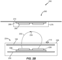
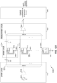
- the wireless power transfer structure 224 (also sometimes referred to as a "pad") is configured to wirelessly transmit or receive power.
- FIG. 2A illustrates one example of a wireless power transfer structure 224 and how the sense element array 106 of FIG. 1 may be integrated.
- the wireless power transfer structure 224 includes a coil 226 also referred to as the wireless power transfer coil that is configured to generate an alternating magnetic field when driven with a current by the power conversion circuit 222.
- the wireless power transfer structure 224 may further include ferrite 228 configured to channel and/or provide a path for magnetic flux ( e.g., may be arranged in one or more ferrite bars which can be a combination of ferrite tiles arranged to form the bars).
- the size of each sense element of the plurality of sense elements 106a, 106b, ..., 106n may be either on the order of this minimum size or a multiple thereof ( e.g., with a 10-times larger area), assuming that those minimum size objects are located in close proximity of a plane defined by the array 106 ( e.g., on the top surface of the housing 236 of the base pad as shown later in FIG. 2B ).
- the number N of sense elements of the array 106 could be on the order of 64 ( e.g., 8 ⁇ 8 array) to be able to provide coverage of the entire predetermined area with the required sensitivity.
- the system shown in FIG. 2A may include a housing (not shown in FIG. 2A but shown later in FIG. 2B as housing 236) configured to house, for example at least the wireless power transfer coil 226, the ferrite 228, the sense element array 106, and potentially the shield 230.
- the housing may be made of any suitable material (e.g., hard plastic, ceramics etc.) and can be designed to provide structural support for example to support the weight of various objects such as vehicles that may pass over the housing.
- the housing may be made of a non-conductive material to avoid interfering or interacting with the magnetic field 232.
- All or just a portion of the power conversion circuit 222 may also be housed in the housing 236. Although in some implementations the power conversion circuit 222 may be housed separately from the housing 236 that houses the wireless power transfer structure 224. In some cases, the power conversion circuit 222 is housed in the housing 236 but is positioned on the other side of the shield 230 from the ferrite 228.
- the shield 230 may form a portion of the housing 236.
- the power conversion circuit 222 is not shown but may be electrically connected to the wireless power transfer coil 226 or a portion or all may also be housed in the housing 236.
- the vehicle-side wireless power receive structure 260 includes a wireless power transfer coil 266, a layer of ferrite 268, and a shield 270 made of an electrically conductive material.
- the shield 270 may be formed from a portion of the apparatus that the ferrite 268 and the wireless power transfer coil 266 are affixed to ( e.g., the metallic underbody of a vehicle).
- a housing 276 configured to house the wireless power transfer coil 266 and ferrite 268 is provided but that would not house the shield 270.
- a shield 270 e.g., a back plate
- a power conversion circuit 222 is not shown but may be electrically connected to the receive coil 268 or a portion or all may also be housed in the housing 276.
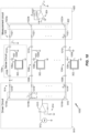
- FIGs. 3 to 8 illustrate examples of different techniques based on measuring at least one electrical characteristic that may be used in conjunction with the object detection circuit 100 of FIG. 1 .
- These examples are to illustrate the principle of the sensing and measurement technique and do not show all the details of an object detection circuit 100. Particularly, they do not show the further signal processing and evaluation circuit as it may be required e.g., for detecting an object based on a change in a measured electrical characteristic.
- these techniques are illustrated by means of a single sense element though applicable to a plurality of sense elements (e.g., sense elements 106a, 106b, ..., 106n) as described below with reference to FIGs. 10 to 14 .
- FIG. 3A shows a circuit 300 to illustrate a technique for inductively sensing a presence of an object 110 based on a change in a complex impedance Z 1 as measured at the terminals of sense coil 302 (e.g., a planar a multi-turn coil) with inductance L 1 that may represent e.g., sense element 106a.
- sense coil 302 e.g., a planar a multi-turn coil
- L 1 may represent e.g., sense element 106a.
- a change ⁇ Z 1 of the impedance Z 1 relative to the impedance Z 1,0 in the absence of the object 110 may indicate a presence of the object 110.
- a change of impedance may be also produced when the sense coil 302 is integrated into the wireless power transfer structure 224 as shown in FIG.
- the circuit 300 of FIG. 3A illustrates a technique for measuring an impedance Z 1 where a sinusoidal current I 1 with a defined frequency, amplitude, and phase provided by a current source 306 is applied to the sense coil 302 and where the open-circuit voltage V 1 across the terminals of the sense coil 302 is measured.
- the open-circuit voltage V 1 is measured using a sensitive high impedance voltage measurement circuit 304 so that there is virtually zero current at the terminals of the voltage measurement circuit 304 ( I 2 ⁇ 0).
- This impedance measurement technique is also referred herein as to the current source voltage measurement approach.
- the current source 306 and the voltage measurement circuit 304 may be part of the measurement and detection circuit 108 with reference to FIG. 1 .
- the voltage measurement circuit 304 may be frequency selective (narrowband) tuned to the sense frequency f s (frequency of the current source) which may be e.g., in the MHz range.
- a change ⁇ Z 1 in the impedance Z 1 e.g., due to presence of the object 110 manifests in a change ⁇ V 1 in the voltage V 1 while the current I 1 remains unaffected. Therefore, measuring a change ⁇ V 1 in the voltage V 1 may be equivalent to measuring a change ⁇ Z 1 in the impedance Z 1 . In other words, the voltage V 1 may be indicative of the impedance Z 1 .
- impedance measurement techniques are also contemplated e.g., by applying a sinusoidal voltage source with a defined voltage V 1 (amplitude and phase) and measuring the current I 1,0 + ⁇ I 1 at the sense coil 302 using a sensitive ( e.g., frequency selective) low impedance current measurement circuit.
- This impedance measurement technique is also referred herein as to the voltage source current measurement approach.
- Equation (3) may apply to the current source (e.g., current source 306) as it may be used in implementations based on any of the impedance or mutual impedance sensing techniques described herein.
- the voltages V 1,0 and ⁇ V 1 in Equation (3) refer to the respective voltages across the output of the current source (e.g ., current source 306) and the currents I 1,0 and ⁇ I 1 to the respective currents at the output of the current source.
- the voltage source in an implementation of the voltage source current measurement approach may be characterized by a quasi-ideal voltage source.
- a quasi-ideal sinusoidal voltage source may be defined as a sinusoidal signal source with a sufficiently small (but non-zero) source impedance so that the magnitude of the fractional change of its output voltage
- Equation(5) may apply to the voltage measurement circuit (e.g., voltage measurement circuit 304) as it may be used in implementations based on any of the impedance and mutual impedance sensing techniques described herein.
- the voltages V 1 and V 1, ⁇ in Equation(5) refer to the respective voltages across the input of the voltage measurement circuit (e.g., voltage measurement circuit 304).
- FIG. 3B An equivalent circuit of the circuit 300 of FIG. 3A including a circuit model of the object 110 is shown in FIG. 3B .
- the sense coil 302 is represented by an equivalent inductance L 1 ( ⁇ ) and an equivalent loss resistance R 1 ( ⁇ ) both shown as a function of temperature ⁇ .
- inductance L 1 ( ⁇ ) may include a change of an inductance due to the presence of materials 310. Depending on the electromagnetic properties of materials 310, this may be a decrease or increase of the inductance L 1 ( ⁇ ) as measured in free space.
- the loss resistance R 1 ( ⁇ ) may include two resistance components.
- a first resistance component may be attributed to the resistance of the sense coil's conductive structure (e.g., copper wires or PCB traces) as experienced at the sense frequency f s (subject of skin and proximity effects).
- a second resistance component may be due to loss effects in materials 310 ( e.g., eddy current and/or hysteresis losses). It may be appreciated that both resistance components may be subject of thermal effects, e.g., they may increase if the temperature inside the housing 236 of the wireless power transfer structure 224 rises.
- the DC resistance of a sense coil's 302 copper winding may vary by 40% for a temperature variation over the range from -20°C to +80°C as it might be specified for an installation in an outdoor environment and assuming a temperature coefficient of 0.004 Q/K for copper and a linear relationship.
- This resistance variation may be smaller (in the order of 20%) at sense frequency f s ( e.g., in the MHz range), taking skin and proximity effects into account, since current distribution inside the sense coil's 302 conductive structure ( e.g., wire) also changes with the electrical conductivity and thus with temperature.
- a similar variation may be expected in the second resistance component if eddy current losses in the materials 310 are the predominant loss effect.
- / R 1 ( ⁇ ) produced by a small object 110 may be in the order of only 0.1% assuming a cost optimized implementation of the object detection circuit 100 of FIG. 1 providing a plurality of sense coils 106a, 106b, and 106 n each with a form factor in the order of 60 x 80 mm.
- This example demonstrates that significant changes in impedance Z over time may occur if the object detection circuit 100 is operated in an outdoor environment.
- object detection may require a differential detection approach (e.g., a time differential detection scheme) rather than detection on an absolute basis (absolute detection) e.g., by comparing the measured impedance Z 1 against a reference value Z 1,ref that has been determined in a process of calibration e.g., at time of installation or commissioning of the wireless power transfer structure 224 as further discussed below.
- a differential detection approach e.g., a time differential detection scheme
- absolute detection absolute basis
- the object 110 is modelled by an equivalent inductance L 3 and an equivalent loss resistance R 3 justified by the fact that an object 110 in general can store and dissipate electrical energy.
- An LR-model may apply to a metallic object 110 that appears electrically conductive but non-ferromagnetic at sense frequency f s . It may not apply to an object 110 that appears ferromagnetic or dielectric at sense frequency f s as further discussed below.
- An object 110 not exhibiting a noticeable ferromagnetic effect (e.g., a magnetic relative permeability ⁇ r > 1 ) at sense frequency f s may be referred to as a non-ferromagnetic object.
- an electrically conductive object 110 that appears ferromagnetic at sense frequency f s is referred to as a ferromagnetic conductive object 110.
- Modelling of a ferromagnetic conductive object 110 may be more complex than shown in FIG. 3B by an equivalent LR circuit model. Magnetic coupling between object 110 and sense coil 302 (between inductance L 3 and inductance L 1 ) is modelled by coupling factor k 13 . Practical experience with many different types of non-ferromagnetic objects 110 shows that variations of position and orientation of the object 110 relative to sense coil 302 mainly affect the coupling factor k 13 but generally have a minor impact on the parameters of its LR model.
- the transformation factor ⁇ 13 is also a scalar and the change in impedance ⁇ Z 1 reflects the conjugate complex of the impedance of the object 110 with respect to the Q-factor or the angle (argument) of the impedance Z 3 .
- a Q-factor may be attributed to the object 110 since the object 110 in general can store and dissipate energy. Eddy currents are induced into a metallic object 110 when subjected to the magnetic sense field as generated by sense coil 302. Energy is stored in the secondary magnetic field produced by the induced eddy currents in the object 110 (inductance L 3 ) and dissipated in its resistance R 3 .
- Equation (10) indicates that presence of a non-ferromagnetic metallic object 110 with finite electrical conductivity, which can be modelled with resistance R 3 > 0 and inductance L 3 > 0, produces a positive Re ⁇ Z 1 ⁇ and a negative Im ⁇ Z 1 ⁇ . Otherwise stated, it produces an increase of equivalent resistance and a decrease (destruction) of equivalent inductance in the circuit 300.
- FIG. 3D illustrates a complex plane 330 or more precisely a complex half plane comprising quadrant 1 and 4 where the impedance changes ⁇ Z 1 (responses) of different types (categories) of objects 110 may occur. More particular, FIG. 3D shows shaded areas (angle ranges) corresponding to different categories of objects 110 where ⁇ Z 1 may be measured at a sense frequency f s ( e.g., in the MHz range) if the object 110 is placed in proximity of the sense coil 302. To emphasize the characteristics of the different categories of objects 110, the angle ranges indicated in FIG. 3D may be not drawn to scale and should be considered qualitative rather than quantitative. The actual angle ranges may also depend on the particular sense frequency f s . Since the Q-factor of some categories of object 110 generally increases with frequency, some areas will move closer to the imaginary axis when the sense frequency f s is increased.
- a non-ferromagnetic object 110 with a well conducting surface may produce a ⁇ Z 1 in the angle range 331 close to the negative imaginary axis in the 4 th quadrant of the complex plane 330 indicating an object 110 with a relatively high Q-factor Q 3 .
- the angle range 332 that is also in the 4 th quadrant may be characteristic for a piece of thin foil or a metallized (aluminum coated) paper.
- the angle range 333 may be typical for the response ⁇ Z 1 of some ferromagnetic steel objects (e.g., nuts). These objects 110 are electrically conductive but also exhibit a relative permeability ⁇ r > 1. The effect of ferromagnetism in these objects 110 may be threefold. First, it may increase the reactance Im ⁇ Z 1 ⁇ of the sense coil 302. Second, it may increase the loss resistance Re ⁇ Z 1 ⁇ compared to an equal but non-ferromagnetic object with the same conductivity ⁇ since skin depth ⁇ reduces thus resistance R 3 increases with increasing permeability ⁇ r as evident from equation (15). Third, since the object 110 is conductive, it may also destroy reactance of the sense coil 302 at the same time.
- the net response produced by some ferromagnetic steel objects 110 may be found close to the real axis in the angle range 333 (e.g., Im ⁇ Z 1 ⁇ ⁇ 0) in the 4 th or in the 1 st quadrant of the complex plane 330.
- some ferromagnetic steel objects 110 e.g., nuts
- the real axis in the angle range 333 e.g., Im ⁇ Z 1 ⁇ ⁇ 0
- such objects 110 may appear as stealth objects 110.
- Ferromagnetic steel objects 110 with a cylindrical shape of diameter d much smaller than its length l may produce a response ⁇ Z 1 in the angle range 334 around 45° in the 1 st quadrant somewhat depending on its orientation relative to the magnetic sense field.
- the ferromagnetic effect increasing a reactance Im ⁇ Z 1 ⁇ may be much larger than the reactance destroying effect of its conductivity.
- These objects 110 may produce an impedance change ⁇ Z 1 with a positive Q-factor Q ⁇ Z 1 close to unity.
- Ferromagnetic non-conductive objects 110 with low resistive losses may produce a response ⁇ Z 1 in the angle range 335 close to the positive imaginary axis corresponding to a high positive Q-factor Q ⁇ Z 1 .
- a similar response ⁇ Z 1 in the angle range 335 may be also produced by dielectric non-conductive objects 110 with low resistive losses (e.g., a human hand, a plastic bottle filled with water).
- Dielectric objects 110 may interact with the sense coil 302 via the electric field generated by the sense coil's 302 self-capacitance that may be modelled by a capacitance C 1, self in parallel to the equivalent circuit of the sense coil 302 (not shown in FIG. 3B but considered merged into the equivalent inductance L 1 ).
- a dielectric non-conductive object 110 with low resistive losses in proximity of the sense coil 302 may generally increase self-capacitance C 1, self resulting in an increase of reactance (Im ⁇ Z 1 ⁇ > 0) as evident from the following equation: L 1 ⁇ L 1 , ex + ⁇ s 2 L 1 , ex 2 C 1 , self , where L 1, ex denotes the sense coil's 302 inductance excluding self-capacitance.
- the sense coil 302 may be used for capacitive sensing of living objects e.g., a human hand, a cat, or any other animal that are predominantly dielectric and that may be located in proximity of sense coil 302. Such use case may require the object detection circuit 100 to discriminate dielectric objects from metallic objects e.g., if rules and procedures for living object detection would differ from those applied to metal object detection.
- the highest loss power density e.g., Watt per unit surface area
- the object detection circuit 100 may be configured to measure an impedance change ⁇ Z 1 with sufficient accuracy at least with respect to its angle arg ⁇ Z 1 ⁇ . Even higher accuracy (e.g., angle fidelity) may be required if an object detection circuit 100 employs a time-differential detection scheme as further described in connection with FIG. 9 .
- a fast (e.g ., abrupt) change ⁇ Z 1 in a sequence (time-series) of consecutively measured impedances Z 1 due to the object 110 brought to proximity of sense coil 302 may cause a time-differential detector to temporarily produce an output indicative for ⁇ Z 1 .
- a fast (e.g., abrupt) change ⁇ Z 1 due to the object 110 removed from the proximity of sense coil 302 may cause the time-differential detector to temporarily produce an output indicative for - ⁇ Z 1 (opposite sign). Therefore, outputs of a time-differential detector may fall in all four quadrants of the complex plane 330, depending on the characteristics ( e.g., impedance) of the object 110 and whether it is brought to or removed from the proximity of the sense coil 302.
- the object detection circuit 100 of FIG. 1 may be configured to provide accurate calibration of the impedance measurement at least with respect to its angle arg ⁇ Z 1 ⁇ . This may be particularly true for implementations of the object detection circuit 100 of FIG. 1 relying on an impedance measurement circuit (e.g., including a quasi-ideal current source 306 and a quasi-ideal voltage measurement circuit 304) that is subjected to measurement errors.
- an impedance measurement circuit e.g., including a quasi-ideal current source 306 and a quasi-ideal voltage measurement circuit 304
- the object detection sensitivity may be defined as the impedance change ⁇ Z 1 as produced in presence of an object 110 normalized to
- This normalized impedance change (sensitivity) is herein also referred to as the fractional change ⁇ Z 1 /
- equation (19) may be expressed solely in terms of coupling factor k 13 and the object's 110 Q-factor Q 3 as follows: ⁇ Z 1 Z 1 , 0 ⁇ k 13 2 Q 3 1 + Q 3 2 1 ⁇ j Q 3 ,
- equation (20) may be rewritten as ⁇ Z 1 Z 1 , 0 ⁇ k 13 2 1 Q 3 ⁇ j Equation (21) shows that the imaginary part of the fractional change ⁇ Z 1 /
- may determine the required dynamic range of the voltage measurement circuit 304. It may be appreciated that detection of objects 110 with a low fractional change
- may also at least partially determine temperature sensitivity of the object detection circuit 100 as a consequence of a temperature dependent impedance Z 1,0 as previously discussed in connection with FIG. 3B .
- Temperature sensitivity may be defined e.g., with respect to the real part as the ratio of an impedance change Re ⁇ ⁇ Z 1,0 ⁇ due to a temperature change ⁇ ⁇ to an impedance change Re ⁇ Z 1 ⁇ produced by the object 110.
- This ratio e.g., with respect to the real part may be also expressed as the ratio of the fractional changes Re ⁇ ⁇ Z 1,0 ⁇ /
- Equation (22) shows that temperature sensitivity with respect to the real part may reduce if the fractional change Re ⁇ Z 1 ⁇ /
- may be increased by reducing the size of the sense coil 302.
- a smaller sense coil size may be used which may result in a larger number of sense coils.
- a sense coil 302 may be implemented with a spread (spiral) winding (as opposed to a more concentrated winding as illustrated in FIG: 3A ) which may provide a larger fractional change
- SNR signal-to-noise ratio
- V 1,n denotes an equivalent r.m.s. noise voltage at sense frequency f s in the bandwidth B m of the voltage measurement circuit 304.
- An equivalent noise voltage source V 1,n (not shown in FIG. 3C ) may be considered in series to the impedance Z 1 in the equivalent circuit of FIG. 3C .
- This equivalent noise voltage source may generally include the effect of various circuit intrinsic and extrinsic noise sources.
- Circuit intrinsic noise may include thermal noise generated by the resistance R 1 and in the voltage measurement circuit 304.
- Noise produced in the voltage measurement circuit 304 may include thermal noise and quantization noise e.g., if the voltage measurement circuit 304 involves an analog-to-digital converter (ADC).
- the circuit intrinsic noise may also include noise generated in the current source 306 e.g., a noise current component producing a noise voltage across impedance Z 1 .
- this noise current may include additive noise, phase noise and amplitude modulated (AM) noise.
- Additive noise may include thermal noise as generated in the circuit of the current source 306. It may also include quantization noise if the current source involves a digital signal synthesizes and a digital-to-analog converter (DAC).
- DAC digital-to-analog converter
- the effect of DAC quantization noise may appear as a deterministic error on the current amplitude rather than a stochastic noise component.
- the amplitude of current I 1 may be modulated by a low frequency noise component with a 1/ f -characteristics, e.g., if the current source 306 involves a DC supply voltage regulator that generates low frequency noise. Therefore, some implementations of the object detection circuit 100 of FIG. 1 use a current source 306 and a voltage measurement circuit 304 optimized with respect to all sort of noise components to maximize a sensitivity (e.g., the SNR as defined by Equation (24)) with respect to circuit intrinsic noise.
- a sensitivity e.g., the SNR as defined by Equation (24)
- Switching noise in the wireless power electromagnetic field produced by the power conversion circuit 222 may be inductively and/or capacitively coupled into sense coil 302 when the wireless power transfer system is active.
- This circuit extrinsic noise component may include wideband and narrowband noise (e.g., harmonics noise). Therefore, in some implementations of a wireless power transfer system 200 including an object detection circuit 100, the power conversion circuit 222 is optimized with respect to noise e.g., by using extra filtering to suppress noise in a sense frequency band.
- the voltage measurement circuit 304 may be configured to minimize the effect of circuit extrinsic noise sources.
- the noise spectrum is monitored with a spectral resolution corresponding to the bandwidth B m of the voltage measurement circuit 304 to identify potential sense frequencies f s with lowest noise level and within some operational frequency limits determined by the object detection circuit 100.
- the object detection circuit 100 may select a sense frequency f s at a frequency providing lowest noise level. Such procedure may be used to maximize the SNR as defined by Equation (24)) with respect to circuit extrinsic noise and thus to maximize sensitivity of the object detection circuit 100 e.g., in presence of switching noise.
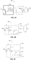
- FIG. 4A shows a circuit 400 illustrating another technique for inductively detecting a presence of an object 110.
- Circuit 400 uses a capacitor 420 having capacitance C to compensate for the reactance ⁇ s L 1 of the sense coil 302 having an inductance L 1 .
- capacitor 420 may not fully compensate for the sense coil's 302 reactance at a specified sense frequency f s ( e.g., in the MHz range).
- the frequency of the current source defining the sense frequency f s may be adjustable so that the LC-circuit may be tuned for improved compensation (resonance) in the absence of an object 110.
- FIG. 4B An equivalent circuit of the circuit 400 of FIG. 4A is illustrated in FIG. 4B .
- the sense coil 302 is represented by an equivalent inductance L 1 ( ⁇ ) and an equivalent loss resistance R 1 ( ⁇ ), and the compensation capacitor 420 by its equivalent capacitance C ( ⁇ ), all three shown as a function of temperature ⁇ .
- inductance L 1 ( ⁇ ) and resistance R 1 ( ⁇ ) may include a change of an inductance and resistance, respectively, due to the presence of materials 310. Depending on the electromagnetic properties of materials 310, this may be a decrease or increase of the inductance L 1 ( ⁇ ) and resistance R 1 ( ⁇ ) as measured in free space.
- the object 110 is abstracted away by impedance change ⁇ Z 1 as previously discussed.
- the impedance Z 1c,0 as measured in absence of object 110 may only include the equivalent resistance R 1 ( ⁇ ).
- equation (26) may be rewritten as ⁇ Z 1 Z 1 c , 0 ⁇ k 13 2 Q 1 1 Q 3 ⁇ j .
- reactance compensation as illustrated by circuit 400 of FIG. 4A may increase sensitivity for various objects.
- impedance measurement may be subjected to measurement errors.
- Reactance compensation may provide a mean for accurate calibration of the impedance measurement e.g., with respect to the angle arg ⁇ Z 12 c ⁇ for purposes as previously discussed in connection with the circuit 300 of FIG. 3A .
- the frequency f s of the current source 306 is tuned such that the magnitude impedance
- the object detection circuit 100 may correct as part of a calibration procedure the actually measured impedance measurement by rotating the impedance plane so that the Im ⁇ Z 1 c ,0 ⁇ vanishes.
- reactance compensation may also allow a sense current I 1 to be increased by a factor of Q 1 , which may in turn result in an increase of the signal-to-noise ratio (SNR) with respect to external noise (e.g., high frequency noise and harmonics in the electromagnetic fields as generated for the wireless power transfer) that is coupled into the sense coil 302.
- SNR signal-to-noise ratio
- reactance compensation using a series capacitor 420 together with a voltage measurement circuit 304 that presents a high input impedance at sense frequency f s and a low impedance at low frequencies may form a high pass filter to attenuate low frequency signal components e.g., at the wireless power transfer frequency f wpt ( e.g., 85 kHz) as described in more detail in connection with FIG. 10 .
- f wpt e.g. 85 kHz
- reactance compensation may not reduce a temperature sensitivity of the object detection circuit 100 as it may be defined in analogy to equations (22) and (23) respectively, since reactance compensation may not reduce a change ⁇ Z 1 c ,0 due to a change in temperature ⁇ ⁇ .
- the change of Im ⁇ ⁇ Z 1 c ,0 ⁇ may be generally larger than Im ⁇ ⁇ Z 1,0 ⁇ if compensation capacitor 420 is also a function of temperature ⁇ .
- temperature sensitivity is reduced by either using a capacitor with a low temperature coefficient (e.g., NP0-type) or with a temperature coefficient that compensates or partially compensates for the temperature drift of the sense coil's impedance Z 1,0 .
- a capacitor with a low temperature coefficient e.g., NP0-type
- a temperature coefficient that compensates or partially compensates for the temperature drift of the sense coil's impedance Z 1,0 e.g., NP0-type
- circuits 300 and 400 of FIGs. 3A and 4A illustrate a technique for detecting an object 110 based on measuring a self-impedance Z 1 or a capacitively compensated self-impedance Z 1 c of a sense coil 302, respectively
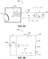
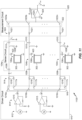
- the circuit 500 of FIG. 5A illustrates another technique for detecting an object 110 based on measuring a transimpedance Z 12 between a first (primary) sense coil 512 with inductance L 1 and a second (secondary) sense coil 514 with inductance L 2 of a sense coil arrangement 510.
- a change ⁇ Z 12 of the transimpedance Z 12 relative to the transimpedance Z 12,0 in the absence of the object 110 may indicate a presence of the object 110 in proximity of at least one of the two sense coils 512 and 514.
- primary sense coil 512 and secondary sense coil 514 of the sense coil arrangement 510 are planar multi-turn coils and are disposed such that there is magnetic coupling between the two sense coils (e.g., sense coils may be overlapping as shown in FIG. 5A ).
- a change of transimpedance ⁇ Z 12 may be also experienced when the two sense coils 512 and 514 are integrated together with the wireless power transfer structure 224 into housing 236 as shown in FIG. 2A due to presence of materials 310 as previously discussed. Presence of materials 310 is indicated in FIG. 5A by the shaded area.
- Materials 310 may also include a dielectric substrate that carries the two sense coils 512 and 516 or a dielectric medium the sense coils are embedded in ( e.g., in case of a printed circuit board (PCB) design).
- the effects of materials 310 may generally produce a change in the sense coils' 512 and 514 self-impedance Z 1,0 and Z 2,0 , respectively, and in the transimpedance Z 12,0 relative to these impedances as measured in free space.
- the effects of materials 310 are considered already included in Z 1,0 , Z 2,0 and Z 12,0 .
- the circuit 500 of FIG. 5A illustrates a technique for measuring a transimpedance Z 12 based on the current source voltage measurement approach.
- a sinusoidal current I 1 with a defined frequency, amplitude, and phase provided by a current source 306 is applied to the primary sense coil 512 and the open-circuit voltage V 2 is measured across the terminals of the secondary sense coil 514.
- the open-circuit voltage V 1 is measured using a sensitive high impedance voltage measurement circuit 304 so that there is virtually zero current at the terminals of the secondary sense coil 514 ( I 2 ⁇ 0).
- the current source 306 and the voltage measurement circuit 304 may be part of the measurement and detection circuit 108 with reference to FIG. 1 .
- the voltage measurement circuit 304 may be frequency selective (narrowband) tuned to the sense frequency f s (frequency of the current source) as previously discussed in connection with the circuit 300 of FIG. 3A .
- measuring a change ⁇ V 2 in the voltage V 2 may be equivalent to measuring a change ⁇ Z 12 in the transimpedance Z 12 .
- the voltage V 2 may be indicative of the transimpedance Z 12 .
- the current source 306 and the voltage measurement circuit 304 used in an implementation of the circuit 500 of FIG. 5A may be characterized by a quasi-ideal current source and a quasi-ideal voltage measurement circuit, respectively, as defined in connection with the circuit 300 of FIG. 3A .
- the transimpedance as measured between a pair of sense coils depends on the measurement technique (e.g., on loading conditions of sense coils 512 and 514).
- the transimpedance as measured with the current source voltage measurement approach illustrated by the circuit 500 of FIG. 5A may be also referred to as the mutual impedance.
- FIG. 5B An equivalent circuit of the circuit 500 of FIG. 5A including a circuit model of the object 110 is shown in FIG. 5B .
- the primary sense coil 512 and secondary sense coil 514 are each represented by an equivalent inductance L 1 ( ⁇ ) and L 2 ( ⁇ ), respectively, and by an equivalent loss resistance R 1 ( ⁇ ) and R 2 ( ⁇ ), all shown as a function of temperature ⁇ .
- the equivalent loss resistances R 1 ( ⁇ ) and R 2 ( ⁇ ) may each include a first resistance component due to losses in the sense coil's conductive structure ( e.g., copper wires or PCB traces) and a second resistance component due to loss effects in materials 310 as previously discussed in connection with FIG. 3B .
- Magnetic coupling between sense coils 512 and 514 is represented by a complex coupling factor k 12 ( ⁇ ), also shown as a function of temperature ⁇ as further explained below.
- the equivalent inductances and resistance L 1 ( ⁇ ), L 2 ( ⁇ ), R 1 ( ⁇ ) and R 2 ( ⁇ ), respectively, as well as the coupling factor k 12 ( ⁇ ) may include a change due to the presence of materials 310. Since the electromagnetic properties of materials 310 may generally be temperature dependent, some temperature dependence may be expected for the coupling factor k 12 ( ⁇ ).
- the change in k 12 ( ⁇ ) due to materials 310 may include a real and imaginary component due to reactive and resistive (loss) effects, respectively, in materials 310 but also due to mutual loss effects e.g., an eddy current loss effect in the secondary sense coil 514 produced by the magnetic field of the primary sense coil 512.
- FIG. 5B shows each of the primary sense coil 512 and the secondary sense coil 514 magnetically coupled with coupling factor k 13 and k 23 , respectively, to the object 110 represented by an LR-Model ( L 3 , R 3 ) as previously discussed e.g. , with reference to FIG. 3B .
- the effect of presence of the object 110 in proximity of coil arrangement 510 may be threefold. First, it produces a change ⁇ Z 1 in the impedance Z 1 as it would be measured at the terminals of sense coil 512. Second, it produces a change ⁇ Z 2 in the impedance Z 2 as it would be measured at the terminals of sense coil 514.
- FIG. 5C shows an equivalent circuit of the circuit 500 of FIG. 5A .
- Each of the three branch impedances is composed of an inductance, resistance and an impedance change due to presence of the object 110. More precisely, the equivalent circuit of FIG. 5B shows the model of the object 110 abstracted away by impedance change ⁇ Z 1 - ⁇ Z 12 and ⁇ Z 2 - ⁇ Z 12 in the first and second series branch impedance Z 1 - Z 12 and Z 2 - Z 12 , respectively, and by a change of mutual impedance ⁇ Z 12 in the shunt branch impedance Z 12 . Though not shown in FIG. 5C for illustrative purposes and simplicity, each of the equivalent circuit elements may be temperature dependent.
- leakage inductances L 1 - M 12 and L 2 - M 12 , equivalent series resistances R 1 - R 12 and R 2 - R 12 , and impedance changes ⁇ Z 1 - ⁇ Z 12 and ⁇ Z 2 - ⁇ Z 12 have ideally no effect in the transimpedance measurement.
- the sensitivity of the object detection circuit 100 of FIG. 1 based on the mutual impedance sensing technique may be defined as the mutual impedance change ⁇ Z 12 as produced in presence of an object 110 normalized to
- This normalized mutual impedance change (sensitivity) may be also referred to as the fractional change ⁇ Z 12 /
- Equation (52) For a sense coil arrangement 510 with high enough mutual inductance ⁇ s M 12 ⁇ R 1 , the magnitude mutual impedance
- equation (54) may be expressed analogously to equation (20) solely in terms of coupling factors k 13 , k 23 , k 12 and the object's 110 Q-factor Q 3 as follows: ⁇ Z 12 Z 12 , 0 ⁇ k 13 k 23 k _ 12 Q 3 1 + Q 3 2 1 ⁇ j Q 3 ,
- equation (55) may be rewritten as ⁇ Z 12 Z 12 , 0 ⁇ k 13 k 23 k _ 12 1 Q 3 ⁇ j
- ⁇ 1 e.g., using two identical sense coils on top of each other and with zero displacement as shown by FIG.
- Equation (57) indicates that the mutual impedance sensing technique has the potential to provide a sensitivity (fractional change) equal to that of self-impedance sensing (Equation (21)) assuming equal coupling to the object 110 for both sensing methods (circuit 300 of FIG. 3A and circuit 500 of FIG. 5A ).
- SNR I 1 2 ⁇ ⁇ Z 1 2 V 1 , n 2 ⁇ I 1 2 ⁇ ⁇ Z 12 2 V 2 , n 2 .
- k 13 ⁇ k 23 e.g., primary and secondary sense coil are physically displaced e.g., as illustrated by FIG. 5D
- a lower SNR may be expected from mutual impedance sensing (circuit 500).
- This feature may allow the object detection circuit 100 to discriminate certain categories of objects and/or increase a sensitivity for certain categories of objects as previously discussed in connection with the self-impedance sensing technique (circuit 300) as illustrated by FIG. 3A .
- transimpedance measurement techniques may be used e.g., the voltage source current measurement approach as previously described in connection with the circuit 300 of FIG. 3A .
- the expression in brackets generally is a non-scalar (complex) transformation factor. Therefore, the change ⁇ Z 12 in transimpedance may be no more proportional to the object's 110 sign-inverted impedance - Z 3 , hence arg ⁇ Z 12 ⁇ ⁇ - arg ⁇ Z 3 ⁇ ). Moreover, the resulting angle arg ⁇ Z 12 ⁇ may vary with position and orientation of the object 110 relative to the sense coil arrangement 510. In some aspects of transimpedance sensing, this finding may be considered as a difficulty of the voltage source current measurement approach.
- the object detection circuit 100 is configured to calibrate the mutual impedance measurements for purposes as previously described in connection with FIGs. 3A to 3D .
- implementation of the calibration may result in higher circuit complexity and cost in certain aspects, e.g., if compared to aspects of capacitively compensated self-impedance sensing using sense frequency tuning as discussed in connection with FIG. 4A .
- FIGs. 5D to 5H are cut views illustrating various exemplary implementations of planar sense coil arrangements 510 as they may be used for transimpedance (e.g., mutual impedance) sensing.
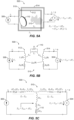
- FIG. 5D illustrates an implementation of a sense coil arrangement 510 where sense coils 512 and 514 are coplanar and adjacent.
- This sense coil arrangement 510 may apply to an implementation using a plurality of substantially equal sense elements 106a, 106b, ... , 106n each including a single planar sense coil arranged in an array 106 with reference to FIG. 2A . Pairs of neighboring sense coils (e.g., sense coil 106a and 106b) may be temporarily configured using a multiplexer circuitry as further discussed with reference to FIG. 10 .
- a first pair may be configured by sense coils 106a and 106b, a second pair may be configured by sense coils 106b and 106c, a third pair may be configured by sense coils 106c and 106d etc.
- Sense coils pairs that are temporarily ( e.g., sequentially) configured may be overlapping. It may be also appreciated that in such implementation or operation, the number of double sense coil arrangements 510 that can be potentially configured is larger than the number N of sense elements of the array 106.
- FIG. 5E illustrates another implementation of a sense coil arrangement 510 where sense coils 512 and 514 are partially overlapping.
- This sense coil arrangement 510 may apply to an implementation using a plurality of substantially equal sense elements 106a, 106b, ..., 106n each including a single planar sense coil arranged in an array 106 having a first and second plane.
- Sense coils in the first plane are offset relative to the sense coils in the second plane by half of the width of the sense coil.
- Pairs of overlapping sense coils e.g., with a primary sense coil 512 in a first plane and a secondary sense coil 514 in a second plane may be temporally ( e.g., sequentially) configured using a multiplexer circuitry as further discussed with reference to FIG.
- a first pair may be configured by sense coil 106a in the first plane and sense coil 106b in the second plane
- a second pair may be configured by sense coil 106b in the second plane and sense coil 106c in the first plane
- a third pair may be configured by sense coils 106c in the first plane and sense coil 106d in the second plane, etc.
- Sense coil pairs temporarily configured in this way may be overlapping.
- FIG. 5F illustrates a further implementation of a sense coil arrangement 510 where sense coils 512 and 514 are fully overlapping (on top of each other).
- This sense coil arrangement 510 may apply to an implementation using a plurality of sense elements 106a, 106b, ..., 106n arranged in an array 106.
- Each of the plurality sense elements 106a, 106b, ... , 106n includes a pair of planar sense coils stacked on top of each other.
- This sense coil arrangement 510 may be also considered as a bifilar winding structure with a first winding disposed in a first plane and a second winding disposed in a second plane.
- FIG. 5G illustrates yet another exemplary implementation of a sense coil arrangement 510 where sense coils 512 and 514 are coplanar and arranged inside of each other.
- This sense coil arrangement 510 may apply to an implementation using a plurality of sense elements 106a, 106b, ..., 106n arranged in an array 106.
- Each sense element includes a pair of coplanar sense coils arranged inside each other.
- FIG. 5H illustrates yet a further implementation of a sense coil arrangement 510 where sense coils 512 and 514 are coplanar and interleaved.
- This sense coil arrangement 510 may apply to an implementation using a plurality of sense elements 106a, 106b, ..., 106n arranged in an array 106 with reference to FIG. 2A .
- Each sense element includes a pair of interleaved coplanar sense coils.
- This sense coil arrangement 510 may be also considered as a bifilar winding structure with a first and a second winding in the same plane.
- FIG. 6A shows a circuit 600 to illustrate another technique based on the mutual impedance sensing approach as previously described with reference to FIGs. 5A to 5H .
- FIG. 6A shows the sense coil 514 displaced relative to the sense coil 512 by an amount D.
- FIG. 6A also indicates a first magnetic flux ⁇ 1 through the overlap area and a second flux ⁇ 2 in the opposite direction through the non-overlap area of sense coil 514.
- There may be a displacement D where the net magnetic flux ⁇ ⁇ ⁇ 1 - ⁇ 2 generated by the primary sense coil 512 and passing through the secondary sense coil 514 is virtually zero (flux balance) resulting in virtually zero coupling (
- perfect flux balance zero coupling
- Losses in materials 310 may cause a small out-of-phase component in the flux ⁇ 2 relative to flux ⁇ 1 so that the net flux ⁇ ⁇ may never vanish entirely for any displacement D within some limits.
- the displacement D between the primary sense coil 512 and secondary sense coil 514 may be adjusted to reduce coupling.
- the level of coupling may be negligible or at least reduced to below a threshold.
- the displacement D may be adjusted by design for minimum magnitude coupling
- a mutual impedance sensing technique operating at or near flux balance may be referred to as flux balanced mutual impedance sensing.
- flux balanced mutual impedance sensing is used to increase a sensitivity (fractional change ⁇ Z 12 /
- a sensitivity fractional change ⁇ Z 12 /
- the sensitivity gain in this example may be quantified approximately by 1/
- FIG. 6B shows a simplified equivalent circuit of the circuit 600 of FIG. 6A .
- the sense coil arrangement 512 is represented by a simplified 'T' equivalent circuit model neglecting first and second series branch impedance as previously described with reference to FIG. 5C .
- This simplification may be permissible for the current source voltage measurement approach, since first and second series branch impedance have virtually no impact in the mutual impedance measurement.
- This simplified equivalent circuit solely comprises the shunt branch impedance Z 12 including the residual mutual inductance M 12 , a residual resistance R 12 , and mutual impedance change ⁇ Z 12 that represents the object 110 abstracted away.
- Flux balanced impedance sensing may be also implemented using a special sense coil arrangement 510 as illustrated by circuit 600 in FIG. 6C .
- FIG. 6C shows the primary sense coil 512 as a "figure eight" or "DD"-type coil while the secondary sense coil 514 is shown as a "circular"-type coil. It may be appreciated that there exist other implementations or combinations providing flux balance in the secondary sense coil 514.
- the primary sense coil 512 is a "circular"-type coil and the secondary 514 is a "DD"-type coil.
- the sense element array 106 is integrated together with the wireless power transfer structure 224 into housing 236 as illustrated by FIG. 2B .
- the design of the sense elements of the plurality of sense elements 106a, 106b, ..., 106n may require some modifications to substantially compensate for the flux unbalancing effects of materials 310 as previously defined in connection with FIG. 3A . These design modifications may be individual for each sense element of the plurality of sense elements 106a, 106b, ..., 106n.
- min may not be achieved in each of the plurality of sense elements e.g., because the integration impact is difficult to predict or may vary over time due to mechanical changes, ageing, temperature variations, etc. resulting in some loss of sensitivity. Therefore, adjusting flux balance in situ may be desirable.
- the sense coil arrangement 510 used for flux balanced mutual impedance sensing, there may exist positions of the object 110 where flux remains virtually balanced even for an object 110 in close proximity to the sense coil arrangement 510, meaning reduced or virtually zero sensitivity ( ⁇ Z 12 ⁇ 0).
- the blind spot (sum of all positions where sensitivity is below a threshold) may be extremely narrow. Therefore, the likelihood that an object 110 comes to a rest in a blind spot may be very low.
- These positions may also somewhat dependent on type, size, and orientation of the object 110.
- the blind spot e.g., for a coin may be found in a narrow area along its vertical symmetry axis (not shown in FIG.
- FIG. 7A shows a circuit 700 illustrating a further technique which may be also referred to as flux balanced mutual impedance sensing.
- the circuit 700 is also based on the current source voltage measurement approach. It includes a sense coil arrangement 710 of two primary sense coils 512 with inductance L 1 and 516 with inductance L 3 and a secondary sense coil 514 with inductance L 2 .
- Each of the primary sense coils 512 and 516 is driven by a first and second current source 306 and 308 delivering currents I 1 and I 2 , respectively, e.g., with a sinusoidal current in the MHz range.
- the secondary sense coil 514 is electrically connected to the voltage measurement circuit 504 for measuring the open-circuit output voltage V 3 .
- the second current source 308 delivering current I 2 is controllable in amplitude and phase so that the circuit 700 may be operated such that the magnetic flux components as generated by sense coil 512 and 516 and passing through the secondary sense coil 514 cancel out (substantially zero flux or at least very low flux) resulting in substantially zero output voltage ( V 3 ⁇ 0) in absence of the object 110.
- FIG. 7 also shows an object 110 at an exemplary position in proximity of the sense coil arrangement 710. Since the output voltage V 3 is a function of two primary currents I 1 and I 2 , the definition of a transimpedance (e.g., Equation (28)) may generally not apply. Therefore, this technique may rely on measuring the output voltage V 3 and the object 110 is detected based on a change ⁇ V 3 in the output voltage V 3 relative to the voltage V 3,0 as measured in absence of the object 110.
- FIG. 7B shows an equivalent circuit of the circuit 700 including equivalent loss resistances R 1 , R 2 , and R 3 of sense coils 512, 516, and 514, respectively.
- Coupling between the first primary sense coil 512 and secondary sense coil 514 and between the second primary sense coil 516 and secondary sense coil 514 is represented by complex coupling factors k 13 and k 23 , respectively, as previously discussed in connection with FIG. 3B .
- Coupling between the two primary sense coils 512 and 516 may also exist but is omitted in FIG. 7B as it generally does not matter for the current source voltage measurement approach.
- It also includes an equivalent circuit model of the object 110 ( L 4 , R 4 ) and corresponding coupling to each sense coil (512, 514, and 516) represented by coupling factors k 14 , k 34 , and k 24 , respectively.
- FIG. 7C shows a simplified equivalent circuit of the circuit 700 to illustrate the voltage cancellation effect in output voltage V 3 .
- This equivalent circuit includes a simplified 'T'-equivalent circuit (transformer) models reduced to the shunt branch (mutual) impedances Z 13 and Z 23 , respectively, for each of the two transmission paths I 1 to V 3 and I 2 to V 3 .
- Each shunt branch impedance Z 13 and Z 23 incudes a mutual inductance M 13 and M 23 , an equivalent loss resistance R 12 and R 23 corresponding to the imaginary part of coupling factor k 13 and k 23 , respectively.
- Each of the shunt branch impedances Z 13 and Z 23 also includes a mutual impedance change ⁇ Z 13 and ⁇ Z 23 representing the model of the object 110 abstracted away.
- FIG. 7C also indicates the two primary currents I 1 and I 2 and the resulting partial voltages V 13 and V 23 across shunt branch impedance Z 13 and Z 23 , respectively.
- the second current source 308 can be precisely adjusted to the required value in terms of both amplitude and phase, perfect voltage cancellation may be achieved.
- Phase adjustment may be needed if materials 310 unequally affect the coupling factors k 13 and k 23 in terms of the loss angle so that arg ⁇ k 13 ⁇ ⁇ arg ⁇ k 23 ⁇ results.
- ⁇ V 3 ⁇ V 13 + ⁇ V 23 ⁇ 0 in presence of the object 110.
- the blind spot may be found along a diagonal line of sense coil 514 corresponding with the symmetry line (not shown in FIG. 7a ) of the sense coil arrangement 710.
- the sense coil arrangement 710 of FIG. 7A may provide sensitivity above the entire area spanned by the three sense coils 512, 514, and 516 and even outside this area to some extent.
- the circuit 700 may provide an infinite sensitivity with respect to the fractional change ⁇ V 3 /
- the circuit 700 potentially allows for angle-true impedance measurement for purposes as previously discussed in connection with FIG. 3D , if the phase angle of the currents I 1 and I 2 are similar (arg ⁇ I 1 ⁇ ⁇ arg ⁇ I 2 ⁇ ). This condition may be satisfied if materials 310 similarly affect the coupling factors k 13 and k 23 in terms of loss angle so that arg ⁇ k 13 ⁇ ⁇ arg ⁇ k 23 ⁇ results.
- either the ratio V 3 / I 1 or the ratio V 3 / I 2 may be used for determining the angle arg ⁇ Z 3 ⁇ of the object's 110 impedance Z 3 .
- the voltage V 3 may be related to the average of the currents I 1 and I 2 .
- sense coils 512, 514, and 516 may correspond e.g., to sense elements 106a, 106b, 106c, respectively, of the sense element array 106 with reference to FIG. 2A .
- sense coil arrangement 710 are temporarily ( e.g., sequentially) configured for flux compensated mutual impedance sensing by three neighboring sense elements ( e.g ., sense elements 106a, 106b, 106c) using a multiplexer circuitry as further discussed with reference to FIG. 11 .
- a first sense coil arrangement 710 may comprise sense coil 106a as the secondary sense coil 514, sense coil 106b as the first primary sense coil 512, and the sense coil 106c as the second primary sense coils 516.
- a second sense coil arrangement 710 may comprise sense coil 106b as the secondary sense coil 514, sense coil 106c as the first primary sense coil 512, and the sense coil 106d as the second primary sense coils 516, etc.
- Sense coil triples temporarily configured in this way may be overlapping.
- Overlapping sense coil arrangements 710 may reduce or eliminate blind spots as previously discussed in connection with FIG. 7C , if the blind spots of the plurality of the sense coil arrangements 710 are non-overlapping (disjoint).
- the number of sense coil arrangements 710 that can be potentially configured is larger than the number N of sense elements of the array 106. Any combination of three sense elements of the plurality of sense elements 106a, 106b, ..., 106n may be potentially used in a sense coil arrangement 710.
- FIGs. 7D to 7H are cut views illustrating various exemplary implementations of planar sense coil arrangements 710 as they may be used for flux balanced mutual impedance sensing.
- FIG. 7D illustrates an implementation of a sense coil arrangement 710 where sense coil 512, 514, and 516 are coplanar and adjacent.
- This sense coil arrangement 710 may apply to an implementation using a plurality of substantially equal sense elements 106a, 106b, ..., 106n each including a single planar sense coil arranged in an array 106 with reference to FIG. 2A .
- Triples of neighboring sense coils e.g., sense coil 106a, 106b, 106c
- FIG. 7E illustrates another exemplary implementation in analogy to FIG. 5E where sense coils 512, 514, and 516 are partially overlapping.
- This sense coil arrangement 710 may apply to an implementation using a plurality of substantially equal sense elements 106a, 106b, ..., 106n, each including a single planar sense coil arranged in an array 106 having a first and a second plane and where the sense coils in the first plane are offset relative to the sense coils in the second plane by half of the width of a sense coil.
- Triples of neighboring sense coils e.g., sense coil 106a, 106b, 106c
- Sense coil triples that are temporarily (e.g ., sequentially) configured may be overlapping. It may be also appreciated that in such implementation or operation, the number of triple sense coil arrangements 510 that can be potentially configured is larger than the number N of sense elements of the array 106.
- FIG. 7F illustrates a further implementation of a sense coil arrangement 710 in analogy to FIG. 5F where sense coils 512, 514, and 516 are fully overlapping (on top of each other).
- This sense coil arrangement 710 may apply to an implementation using a plurality of sense elements 106a, 106b, ..., 106n arranged in an array 106.
- Each of the plurality sense elements 106a, 106b, ..., 106n includes a triple of planar sense coils stacked on top of each other.
- This sense coil arrangement 710 may be also considered as a trifilar winding structure with a first winding disposed in a first plane and a second and third winding disposed in a second and third plane, respectively.
- FIG. 7G illustrates yet another implementation of a sense coil arrangement 710 in analogy to FIG. 5G where sense coil 512, 514, and 516 are coplanar and arranged inside of each other.
- This sense coil arrangement 710 may apply to an implementation using a plurality of sense elements 106a, 106b, ..., 106n arranged in an array 106.
- Each sense element includes a triple of coplanar sense coils arranged inside each other.
- FIG. 7H illustrates yet a further implementation in analogy to FIG. 5H where sense coil 512, 514, and 516 are coplanar and interleaved.
- This sense coil arrangement 710 may apply to an implementation using a plurality of sense elements 106a, 106b, ..., 106n arranged in an array 106. Each sense element includes a triple of interleaved coplanar sense coils.
- This sense coil arrangement 710 may be also considered as a trifilar winding structure with a first, a second, and a third winding in the same plane.
- FIG. 7D and 7E may provide a substantial net response ⁇ V 3 in presence of the object 110
- the implementations of FIGs. 7E to 7H may not. This may be particularly true for an implementation based on FIG. 7F with a relatively small vertical spacing between the three sense coils 512, 514, and 516.
- the object 110 affects the mutual impedances Z 13 and Z 23 almost equally ( ⁇ Z 13 ⁇ ⁇ Z 23 ). Since Z 13 ⁇ Z 23 and thus I 1 ⁇ - I 2 , a very low net response ⁇ V 3 may result in presence of the object 110 as evident from Equation (60). This may be true for any position of the object 110.
- the object detection circuit 100 is configured to calibrate the mutual impedance measurement for purposes as previously described in connection with FIGs. 3A to 3D .
- implementation of such calibration may require higher circuit complexity and cost in certain aspects, e.g., compared to aspects of capacitively compensated self-impedance sensing using sense frequency tuning as discussed in connection with FIG. 4A .
- a technique that combines several advantages as previously discussed with reference to FIGs. 4A and 5A and that avoids certain issues related to blind spots as previously discussed with reference to FIGs. 6A and 6C is illustrated by the circuit 800 of FIG. 8A .
- This technique is referred to as capacitively compensated mutual impedance sensing.
- the circuit 800 is also based on the current source voltage measurement approach.
- a sense coil arrangement 510 is used for sensing the object 110.
- the sense coil arrangement 510 includes a primary sense coil 512 with inductance L 1 and a secondary sense coil 514 with inductance L 2 , each having a first and second terminal.
- the circuit 800 further includes a capacitor 820 (compensation or tuning capacitor) with capacitance C.
- the capacitor 820 has a first and second terminal.
- the first terminal of the capacitor 820 is electrically connected to the second terminals of each of the sense coils 512 and 514.
- the circuit 800 includes an alternating current source 306 that is tunable in frequency and that drives a current I 1 at sense frequency f s into the primary sense coil 512.
- the current source 306 is electrically connected to the first terminal of the primary sense coil 512 and to the second terminal of the capacitor 820 (in some implementations the second terminal of the capacitor 820 is electrically connected to a reference ground potential).
- the voltage measurement circuit 304 is electrically connected to the first terminal of the secondary sense coil 514 and to the second terminal of the capacitor 820.
- the voltage measurement circuit 304 may be frequency selective (narrowband) tuned to the sense frequency f s .
- FIG. 8A also indicates presence of materials 310 by the shaded area.
- FIG. 8B An equivalent circuit of the circuit 800 of FIG. 8A including a circuit model of the object 110 is shown in FIG. 8B .
- the primary sense coil 512 and secondary sense coil 514 are each represented by an equivalent inductance L 1 and L 2 , respectively, and by an equivalent loss resistance R 1 and R 2 .
- each of these elements may be a function of temperature ⁇ .
- the equivalent loss resistances R 1 and R 2 may each include a first resistance component due to losses in the sense coil's conductive structure (e.g., copper wires or PCB traces) and a second resistance component due to loss effects in materials 310 as previously discussed in connection with FIG. 3B .
- Magnetic coupling between sense coils 512 and 514 is represented by a complex coupling factor k 12 , which may be also a function of temperature ⁇ as previously explained in connection with FIGs. 5B and 5C .
- the equivalent inductances and resistance L 1 , L 2 , R 1 and R 2 , respectively, as well as the coupling factor k 12 may include a change due to the presence of materials 310. Since the electromagnetic properties of materials 310 may generally be temperature dependent, some temperature dependence may be expected for the coupling factor k 12 .
- the change in k 12 due to materials 310 may include a real and imaginary component due to reactive and resistive (loss) effects, respectively, in materials 310 but also due to mutual loss effects in the sense coils 512 and 514 as previously discussed.
- the real component relates to the mutual inductance M 12 defined by Equation (29) while the imaginary component relates to an equivalent mutual resistance R 12 defined by Equation (31).
- FIG. 8B shows each of the primary sense coil 512 and the secondary sense coil 514 magnetically coupled with coupling factor k 13 and k 23 , respectively, to the object 110 represented by an LR-Model ( L 3 , R 3 ) as previously discussed e.g., with reference to FIG. 3B .
- the compensation capacitor appears with its equivalent capacitance C that may be also a function of temperature ⁇ depending on the type of capacitor as previously discussed in connection with FIG. 4A .
- FIG. 8C shows a simplified equivalent circuit of the circuit 800 of FIG. 8A .
- the sense coil arrangement 512 is represented by a simplified "T" equivalent circuit model neglecting first and second series branch impedance as previously discussed with reference to FIG. 6B .
- This simplified equivalent circuit solely comprises the shunt branch impedance that is now referred to as the capacitively compensated mutual impedance Z 12 c . It includes the mutual inductance M 12 , the equivalent mutual resistance R 12 , the capacitance C that appears now in series to mutual inductance M 12 , and the equivalent mutual impedance change ⁇ Z 12 that represents the object 110 abstracted away.
- This condition may also be considered as some sort of resonance and may be achieved by tuning the frequency f s of the current source so that the magnitude of the mutual impedance Z 12 c in absence of the object 110 denoted by
- equation (74) may be rewritten as ⁇ Z 12 Z 12 c , 0 ⁇ k 13 k 23 k _ 12 Q 12 1 Q 3 ⁇ j showing that the fractional change
- Equation (75) may be rewritten as ⁇ Z 12 Z 12 c , 0 ⁇ k 13 2 Q 12 1 Q 3 ⁇ j
- Equation (29) Equation (29)
- M 12 ⁇ L 1 L 2
- Equation (73) Equation (73)
- each of the sense coils 512 and 514 of the circuit 800 of FIG. 8A identical (or substantially similar) to the sense coil 302 of the circuit 400 of FIG.
- This loss resistance component may be diminished by keeping a small vertical distance between the two sense coils 512 and 514 ( e.g., in sense coil arrangement 510 of FIG. 5F ) such that
- a small vertical distance between the two sense coils 512 and 514 is provided to diminish the loss resistance.
- a gain in Q-factor by a factor of four was found in a non-optimized experimental set-up integrated into a wireless power transfer structure 236 using identical sense coils with equal length lead lines for all sense coils 512, 514, and 302.
- mutual impedance measurement may be subjected to measurement errors.
- reactance compensation e.g ., in the circuit 400 of FIG. A
- mutual reactance compensation may provide a mechanism for accurate calibration of the mutual impedance measurement e.g ., with respect to the angle arg ⁇ Z 12 c ⁇ for purposes as previously discussed in connection with the circuit 300 of FIG. 3A .
- compensation capacitor 820 together with current source 306 and a voltage measurement circuit 304 each presenting a high input impedance at sense frequency f s and a low impedance at low frequencies may form a high pass filter to attenuate low frequency signal components e.g ., at the wireless power transfer frequency f wpt as described in more detail in connection with FIG. 12 .
- This may result in relaxed requirements for the voltage measurement circuit 304 and the current source 306 with respect to the dynamic range, overvoltage capability, etc. as previously discussed in connection with the circuit 400 of FIG. 4A .
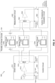
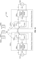
- FIG. 9 is a block diagram of a circuit 900 illustrating example implementations or operations of an object detection circuit 100.
- the block diagram may apply to any of the impedance and transimpedance (e.g., mutual impedance) sensing techniques and variants thereof as described with reference to FIGs. 3A to 8A as well as to various impedance or transimpedance measurement approaches (e.g., the current source voltage measurement approach as previously described with reference to FIG. 3A and 5A ).
- the circuit 900 includes a driver circuit 910, a control circuit 950 associated with the driver circuit 910, a plurality of sense circuits 104, a measurement circuit 920, and a control, processing & evaluation circuit 960 associated with the measurement circuit 920.
- Each sense element may include one or more sense coils (e.g., a sense coil arrangement 510 as it may be required by some of the mutual impedance sensing techniques as previously described with reference to FIGs. 5A to 8A ).
- the plurality of sense elements 106a, 106b, ..., 106n may be arranged in an array ( e.g ., array 106 as previously described with reference to FIGs. 1 and 2A ).
- the object detection circuit 100 of FIG. 1 using capacitive compensation of an impedance or a mutual impedance as described with reference to FIGs.
- each of the plurality of the sense circuits 104a, 104b, ..., 104n may include a compensation (tuning) capacitor (e.g ., capacitor 420 or 820 as shown in FIG. 4A or 8A , respectively).
- Each of the plurality of sense circuits 104a, 104b, ..., 104n may be tuned substantially to a nominal sense frequency. In some implementations, there is a nominal sense frequency common to each of the plurality of sense circuits 104a, 104b, ..., 104n. In other implementations, sense circuits of the plurality of sense circuits 104a, 104b, ..., 104n are intentionally or unintentionally tuned to different nominal sense frequencies.
- the driver circuit 910 (e.g., a portion of the current source 306 with reference to FIG. 3A ) is electrically connected to the plurality of sense circuits 104a, 104b, ..., 104n.
- the driver circuit 910 is configured to operate as a current source (e.g., current source 306 as described in connection with FIG. 3A ) and selectively ( e.g., sequentially) apply a sense current signal I 1 (as indicated in FIG. 9 ) at an operating (sense) frequency f s to each of the plurality of sense circuits 104a, 104b, ..., 104n.
- the driver circuit 910 is configured to operate as a voltage source e.g ., as described in connection with FIG. 3A and selectively ( e.g ., sequentially) apply a sense voltage signal V 1 (as indicated in FIG. 9 ) at an operating (sense) frequency f s to each of the plurality of sense circuits 104a, 104b, ..., 104n.
- the driver circuit 910 is configured to operate as a source that may be characterized neither by a current source nor a voltage source.
- the driver circuit 910 may generate a sinusoidal sense signal with a defined frequency, amplitude and phase.
- the following descriptions of the circuit 900 of FIG. 9 assume a sinusoidal sense signal.
- other sense signal waveforms may be used in certain implementations as previously discussed in connection with FIG. 3A .
- the driver circuit 910 may be configured to generate and apply more than one sense signal (e.g., sense current signal I 1 ) at a time as it may be required in some implementations or operations of an object detection circuit 100.
- the concurrently applied sense signals may generally differ in frequency and amplitude.
- a driver circuit 910 capable of concurrently generating and applying a plurality of sense signals with different (distinct) sense frequencies f s may be used in some implementations or operations of the object detection circuit 100 e.g., to expedite an impedance measurement in each of the plurality of sense circuits 104a, 104b, ..., 104n and/or to expedite a transimpedance measurement in each of a plurality of sense circuit pairs e.g ., in an implementation where each sense circuit includes a single sense coil ( e.g ., sense coil 512 or 514) as discussed with reference to FIG. 5D .
- each sense circuit includes a single sense coil (e.g ., sense coil 512 or 514) as discussed with reference to FIG. 5D .
- a driver circuit 910 configured to provide two outputs (e.g ., current source outputs) each delivering a sinusoidal signal (e.g ., sense current signal I 1 ) with the same frequency f s but generally different amplitude and phase may be used to accomplish flux balanced mutual impedance sensing as described with reference to FIG. 7A .
- An example implementation of a driver circuit 910 configured to provide two current source outputs delivering respective current signals I 1 a and I 1 b is illustrated by FIG. 11 .
- a control circuit 950 electrically connected to the driver circuit 910 is shown for illustrative purposes to indicate control of the driver circuit 910.
- the measurement circuit 920 is electrically connected to each of the plurality of sense circuits 104a, 104b, ..., 104n.
- the measurement circuit 920 is configured to selectively ( e.g ., sequentially) measure an electrical voltage V 2 (as indicated in FIG. 9 ) in each of the plurality of sense circuits 104a, 104b, ..., 104n and to provide a measurement output V out proportional to the electrical voltage V 2 .
- the measurement output V out is proportional to an electrical voltage V 2 in one of the plurality of sense circuits 104a, 104b, ..., 104n in response to the at least one sense current signal I 1 being applied by the driver circuit 910 to the respective at least one sense circuit of the plurality of sense circuits 104a, 104b, ..., 104n.
- the measurement circuit 920 is configured to selectively ( e.g ., sequentially) measure an electrical current I 2 (as indicated in FIG. 9 ) in each of the plurality of sense circuits 104a, 104b, ..., 104n and to provide a measurement output V out proportional to the electrical current I 2 .
- the measurement output V out is proportional to an electrical current I 2 in one of the plurality of sense circuits 104a, 104b, ..., 104n in response to the at least one sense voltage signal V 1 being applied by the driver circuit 910 to the respective at least one sense circuit of the plurality of sense circuits 104a, 104b, ..., 104n.
- the measurement circuit 920 is an analog front-end portion of a more complex measurement circuit that also encompasses functions included in the control, processing & evaluation circuit 960.
- the measurement circuit 920 may include a multiplexer (e.g ., multiplexer 922) and an amplifier (e.g ., amplifier 924) as illustrated in FIG. 9 by dashed lines.
- the measurement circuit 920 is configured to measure more than one voltage V 2 or current I 2 at a time and to provide more than one respective measurement output V out .
- Concurrent multiple voltage or current measurement may be required in some implementations or operations of the object detection circuit 100 e.g., to expedite an impedance and/or a transimpedance and/or a flux compensated mutual impedance measurement in each of the plurality of sense circuits 104a, 104b, ..., 104n and/or in pairs and/or even in triples of sense circuits, respectively, of the plurality of sense circuits 104a, 104b, ..., 104n as previously discussed in the context of the driver circuit 910.
- measurement of a plurality of voltages V 2 or currents I 2 is performed concurrently and frequency selectively at the respective frequency f s of each of the plurality of sense signals I 1 or V 1 that is selectively applied to the plurality of sense circuits 104a, 104b, ..., 104n.
- a control, processing & evaluation circuit 960 electrically connected to the measurement circuit 920 is shown for illustrative purposes to indicate control of the measurement circuit 920 and the further processing.
- FIG. 9 assume example implementations based on the current source voltage measurement approach as described with reference to FIG. 3A . However, this should not exclude other impedance or transimpedance measurement approaches (e . g ., voltage source current measurement approach) that may apply.
- impedance or transimpedance measurement approaches e . g ., voltage source current measurement approach
- the driver circuit 910 is configured to operate as at least one current source (e.g., characterized by a quasi-ideal current source as previously defined in connection with FIG. 3A ) and selectively (e.g., sequentially) apply at least one sense current signal I 1 with a defined amplitude and phase at an operating frequency (sense frequency) f s to each of the plurality of sense circuits 104a, 104b, ..., 104n.
- a current source e.g., characterized by a quasi-ideal current source as previously defined in connection with FIG. 3A
- selectively e.g., sequentially
- apply at least one sense current signal I 1 with a defined amplitude and phase at an operating frequency (sense frequency) f s to each of the plurality of sense circuits 104a, 104b, ..., 104n.
- only one sense circuit of the plurality of sense circuits 104a, 104b, ..., 104n is driven at a time.
- the driver circuit 910 may include components such as at least one signal source 912 (e.g., generating the sinusoidal sense signal with a defined frequency f s , amplitude and phase), at least one driver amplifier circuit 914, and at least one multiplexer circuit 916 also referred to as the input multiplexer.
- the at least one driver amplifier circuit 914 is configured to provide a current source output characterized e.g., as a quasi-ideal current source suitable for selectively driving each of the plurality of sense circuits 104a, 104b, ..., 104n based on a signal received from the respective signal source 912.
- the at least one multiplexer circuit 916 may be electrically connected between the output of the respective driver amplifier circuit 914 and the plurality of sense circuits 104a, 104b, ..., 104n and is configured to selectively connect each of the plurality of sense circuits 104a, 104b, ..., 104n to the output of the respective driver amplifier circuit 914.
- the driver circuit 910 may also return at least one reference signal to the control circuit 950. This at least one reference signal may be representative for the respective sense current signal I 1 in terms of frequency, amplitude, and phase.
- This at least one reference signal may be used in the control, processing & evaluation circuit 960 e.g., for computing at least one ratio V out / I 1 (complex value) that may relate to an impedance or a transimpedance ( e . g. , a mutual impedance).
- the control, processing & evaluation circuit 960 may be configured to provide analog-to-digital signal conversion, frequency selective filtering, synchronous detection, combining outputs, summation of outputs, averaging of outputs, scaling of outputs, correction of outputs, evaluation of sequences (time-series) and/or patterns of outputs indicative of an impedance and/or transimpedance ( e.g ., mutual impedance), etc. and eventually to decide whether an object (e.g ., object 110 of FIG.
- 3A is proximate to at least one sense element of the plurality of sense elements 106a, 106b, ..., 106n based on a change in an impedance or transimpedance (e.g., mutual impedance) and to output at least a detection hypothesis H out as indicated in FIG. 9 .
- an impedance or transimpedance e.g., mutual impedance
- the detection hypothesis H out may be indicative for presence or absence of an object (e.g., object 110) and may be used by the wireless power transfer system 200 with reference to FIG. 2A to control wireless power transfer.
- a positive detection hypothesis H out may be indicative for presence of an object (e.g., object 110) and may cause the wireless power transfer system 200 to cease wireless power transfer or to reduce a level of power.
- a negative detection hypothesis H out may be indicative for absence of an object and may cause the wireless power transfer system 200 to continue or resume wireless power transfer or to return to the ordinary power level.
- the detection hypothesis output H out may include additional information (e.g., the position of the at least one sense element associated to a positive hypothesis output H out and/or a detection confidence value).
- the control, processing & evaluation circuit 960 processes at least one sequence (time-series) of consecutive measurement outputs V out each associated to the same at least one sense circuit (e.g ., sense circuit 104a or pair of sense circuits 104a and 104b) of the plurality of sense circuits 104a, 104b, ..., 104n to determine a level of correlation between the at least one first sequence of consecutive measurement outputs V out and a corresponding second sequence indicative of the applied exposure magnetic field signal. Presence of an object (e . g ., object 110) is assumed if the level of correlation exceeds a threshold for at least one sense circuit or at least one pair of sense circuits of the plurality of sense circuits 104a, 104b, ..., 104n.
- Presence of an object e . g ., object 110
- Presence of an object is assumed if the level of correlation exceeds a threshold for at least one sense circuit or at least one pair of sense circuits of the plurality of sense circuits 104
- inductive ferromagnetic sensing is combined with a space-differential detection scheme. Presence of an object (e.g ., object 110) is assumed if at least one difference between the correlator output associated to at least one first sense circuit (e.g ., sense circuit 104a) and the correlator output associated to at least one second sense circuit (e.g ., sense circuit 104b) exceeds a threshold. In another example implementation or operation, respective correlator outputs obtained with inductive ferromagnetic sensing and with inductive thermal sensing are combined.
- Inductive kinematic sensing may be a further specialized detection scheme for detecting an object (e.g., object 110) by its relative motion e.g., when the object is mechanically moved relative to the sense elements (e.g ., the plurality of sense elements 106a, 106b, ..., 106n).
- the top surface of the housing 236 of the wireless power transfer structure 224 where an object may rest is mechanically moved back and forth relative to the sense element array 106.
- the relative movement of an object (e.g., object 110) in proximity of a sense element (e.g., sense element 106a) may produce a time-varying change in an electrical characteristic (e.g., impedance Z 1 , mutual impedance Z 12 ) and thus in the measurement output V out .
- an electrical characteristic e.g., impedance Z 1 , mutual impedance Z 12
- this change (response) in an electrical characteristic will generally be a function of the object's instantaneous position relative to the sense element array 106. This function may be a non-linear function.
- presence of an object is determined based on a correlation between the at least one first sequence of consecutive measurement outputs V out each associated to the same at least one sense circuit (e.g., sense circuit 104a or pair of sense circuits 104a and 104b) of the plurality of sense circuits 104a, 104b, ..., 104n and a corresponding second sequence indicative of the mechanical movement signal.
- sense circuit 104a or pair of sense circuits 104a and 104b e.g., sense circuit 104a or pair of sense circuits 104a and 104b
- Inductive kinematic sensing may potentially provide a solution for detecting objects of any category e.g ., as described with reference to FIG. 3D on an absolute basis as defined above.
- the control, processing & evaluation circuit 960 processes at least one first sequence of consecutive measurement outputs V out each associated to the same at least one sense circuit (e.g., sense circuit 104a or pair of sense circuits 104a and 104b) of the plurality of sense circuits 104a, 104b, ..., 104n to determine a level of correlation between the at least one first sequence of consecutive measurement outputs V out and a corresponding second sequence indicative of the mechanical movement signal. Presence of an object (e.g ., object 110) is assumed if the level of correlation exceeds a threshold for at least one sense circuit or at least one pair of sense circuits of the plurality of sense circuits 104a, 104b, ..., 104n.
- Presence of an object e.g ., object 110
- inductive kinematic sensing is combined with a space-differential detection scheme. Presence of an object (e.g., object 110) is assumed if at least one difference between the correlator output associated to at least one first sense circuit (e.g ., sense circuit 104a) and the correlator output associated to at least one second sense circuit (e.g ., sense circuit 104b) exceeds a threshold.
- correlator outputs obtained with inductive kinematic sensing, inductive thermal sensing, and inductive ferromagnetic sensing are combined.
- an object detection circuit 100 In some implementations or operations of an object detection circuit 100, one or more specialized detection schemes as described above are applied initially before starting regular wireless power transfer e.g ., for the purpose of charging an electric vehicle. If the object detection circuit 100 determines presence of an object (e.g ., object 110), the wireless power transfer system 200 stops detection based on a specialized detection scheme and does not start regular wireless power transfer. During regular wireless power transfer, the object detection circuit 100 may employ at least one other detection scheme e.g., a time-differential scheme capable of detecting an object ( e.g. , object 110) when it enters the predetermined space.
- a time-differential scheme capable of detecting an object (e.g. , object 110) when it enters the predetermined space.
- one or more specialized detection schemes as described above are applied in the event that the object detection circuit 100 trips during regular wireless power transfer.
- one or more specialized detection schemes may be used to verify this detection by first ceasing regular power transfer and then reapplying one or more specialized detection schemes. This may apply in case of a detection with low confidence. If the previous finding of presence of an object (e.g ., object 110) is confirmed, the wireless power transfer system 200 discontinues regular wireless power transfer else it reactivates regular wireless power transfer.
- control circuit 950 and/or the control, processing & evaluation circuit 960 are configured to perform calibration for purposes of determining reference values as previously described for purposes of threshold detection. In further aspects, they may be configured to perform calibration of the impedance or transimpedance measurement with respect to the angle (e.g., arg ⁇ Z 1 ⁇ ) as previously described with reference to the circuit 300 of FIG. 3A .
- control circuit 950 and/or the control, processing & evaluation circuit 960 are configured to perform functions such as finding optimum sense frequencies f s minimizing the effect of circuit extrinsic noise as previously described with reference to the circuit 300 of FIG. 3A .
- the driver circuit 910 is configured to concurrently generate and selectively (e.g., sequentially) apply a plurality of current signals I 1 each with a distinct frequency f s .
- Each of the plurality of current signals I 1 is selectively ( e.g ., sequentially) applied to each of a subset of the plurality of sense circuits 104a, 104b, ..., 104n.
- the number of subsets may equal the number of concurrently applied current signals I 1 .
- such multiple current signal operation may be used to expedite impedance and/or transimpedance measurements in each of a plurality of sense circuits and/or in each of a plurality of pairs of sense circuits, respectively, of the plurality of sense circuits 104a, 104b, ..., 104n.
- an intermodulation product generated by the first and second current signal I 1 having a first and second frequency f s may fall onto the third frequency f s of the third current signal I 1 , thus interfering e.g., in the measurement circuit 920 with the voltage signal V 2 in response to the third current signal I 1 .
- Interference caused by intermodulation products generally manifests in variations in a sequence (time-series) of consecutive measurement outputs V out associated to the same at least one sense circuit (e.g ., sense circuit 104a or pair of sense circuits 104a and 104b). If measurement outputs V out refer to an output (not shown in FIG.
- these variations may be generally characterized by variations in a magnitude and phase. These variations may resemble the effects of circuit intrinsic or extrinsic noise sources as previously discussed with reference to FIG. 3A . However, the variance caused by intermodulation interference may be significantly larger than that produced e.g. , by circuit intrinsic noise. These variations may require the detection threshold to be increased e.g ., in an implementation or operation based on a time-differential detection scheme as described below, thus resulting in lower detection sensitivity.
- interference caused by intermodulation effects is mitigated by a smart selection of sense frequencies f s e.g., by selecting a set of frequencies whose intermodulation products (e.g., up to the fourth order) do not fall on any of the frequencies f s of the selected set of frequencies.
- this approach may put some constraints on the choice of sense frequencies f s .
- the number of concurrently applied currents I 1 is greater than three and in implementations or operations where sense circuits have to be operated at or near resonance, have tolerances with respect to the resonant frequency, and where some frequency bands e.g., jammed by frequency selective switching noise have to be avoided for purposes as previously discussed.
- interference due to intermodulation effects is mitigated by choosing sense frequencies f s for the plurality of concurrently applied current signals I 1 from a set of frequencies with a fixed frequency spacing ⁇ f (e.g., a frequency grid).
- each sense frequency f s is a multiple of the frequency spacing ⁇ f (e.g., 1 kHz). It may be appreciated that the plurality of current signals I 1 with sense frequencies f s differing by integer multiples of ⁇ f generates intermodulation products with frequencies that are also an integer multiple of ⁇ f , thus may potentially fall on one or more sense frequencies f s .
- phase of each of the plurality of concurrently applied current signals I 1 is controlled in a manner so that any intermodulation product falling on a sense frequencies f s produces a static offset (instead of noise-like variations) in sequences (time-series) of consecutive measurement outputs V out associated to the same at least one sense circuit (e.g., sense circuit 104a or pair of sense circuits 104a and 104b).
- a small static offset e.g ., equivalent to a fractional change below 1%) as it may be caused by intermodulation effects may not negatively impact operation of an object detection circuit 100. This may be particularly true for implementations or operations employing a time-differential detection scheme.
- control, processing & evaluation circuit 960 is configured to use the extracted low frequency component as supplementary information being indicative of presence and level of the low frequency magnetic field at wireless power transfer frequency f wpt e.g., to improve the evaluation of measurement outputs V out to determine presence of an object (e.g., object 110).
- this improvement may include adaptation of a threshold e.g., to reduce a false detection rate e.g., due to external noise at sense frequency f s generated by the power conversion circuit 222 with reference to FIG. 2A , which may accompany the low frequency magnetic field.
- the component at f wpt in the voltage V 2 across the sense circuit (e.g., sense circuit 104a) may be only 30 mV while the wanted signal component at sense frequency f s may be in the order of 100 mV.
- the second capacitor 1006 may be needed in some implementations to block any residual DC flow at the output of the driver circuit 910 ( e.g., due to a DC offset).
- the capacitor 1006 may also help to attenuate any residual low frequency current component ( e.g., at a wireless power frequency f wpt ) at the output of the driver circuit 910.
- the third capacitor 1010 may be needed in some implementations to block any residual DC flow at the input of the measurement circuit 920 ( e.g., due to a DC offset).
- the capacitor 1010 may also help to attenuate any residual low frequency current component (e.g., at a wireless power frequency f wpt ) at the input of the measurement circuit 920. Moreover, in some implementations, it may be also used to compensate or partially compensate for the effect of the reactance of shunt inductor 1008 in the measured impedance Z 1 c .
- series resistor 1018 with a large enough resistance R ser 1 potentially transforms the voltage source output (virtually zero source impedance) of the driver amplifier circuit 914 into a quasi-ideal current source 306 (high source impedance) with reference to FIG. 3A .
- a series resistor 1018 with a very large resistance R ser 1 may provide an almost ideal current source characteristic but may also result in a too low sense current I 1 and thus in insufficient SNR as it may be seen from Equation (58). Therefore, in some implementations, the resistance R ser 1 may be a trade-off between the quality of the current source ( e.g ., as specified with reference to FIG. 3A ) and the resulting SNR.
- the numerical result of Equation (82) indicates that this example implementation of a driver circuit 910 satisfies the requirements specified by Equation (2).
- the driver circuit 910 has the potential to drive more than one sense circuit with a current I 1 at a time, each having the same frequency f s and substantially the same amplitude and phase. If e.g. , switch 1016a and 1016b are closed, each of the sense circuits 104a and 104b is driven with a current I 1 .
- the input multiplexer circuit 916 includes a plurality of switches 1016a, 1016b, ..., 1016n and is configured to selectively connect each of the plurality of sense circuits 104a, 104b, ..., 104n via series resistor 1018 to the driver amplifier circuit 914 to selectively ( e.g ., sequentially) drive each of the plurality of sense circuits 104a, 104b, ..., 104n with a sense current I 1 at a sense frequency f s . Therefore, each of the plurality of switches 1016a, 1016b, ..., 1016n is electrically connected to a common input node that is electrically connected to the output of the driver amplifier circuit 914.
- Each of the plurality of switches 1016a, 1016b, ..., 1016n may be one of a semiconductor analog switch (e.g ., a single FET switch, a complementary FET switch composed of a p-channel and a n-channel type FET), a micro-mechanical (MEMS) switch or any other type of switch providing a sufficiently high current signal attenuation in the off-state.
- An analog switch e.g ., a complementary FET switch
- An analog switch may be modelled by an on-state series resistance R sw , an off-state series capacitance C sw , a first and a second parasitic shunt capacitance C sh 1 and C sh 1 , respectively, as indicated in FIG.
- the total capacitive load produced by the plurality of first shunt capacitances C sh 1 may not noticeably impair the current source characteristic of the driver circuit 910 since it is in parallel to the voltage source output (virtually zero source impedance) of the driver amplifier circuit 914. This may be true as long as the operational amplifier 1015 can handle the resulting total capacitive load. Assuming operations where only one or a few switches of the plurality of switches 1016a, 1016b, 1016n are closed at a time, the total capacitive load at the common input node is governed by the plurality of first capacitances C sh 1 .
- an operational amplifier 1025 e.g., a low noise operational amplifier
- This circuit transforms an input current I in into an output voltage V out proportional to I in . Since the voltage at the negative input of operational amplifier 1025 is virtually zero (virtual ground), the measurement amplifier circuit 924 exhibits a virtually zero input impedance.
- the measurement amplifier circuit 924 together with series resistors 1021 mimic a quasi-ideal voltage measurement circuit 304 with reference to FIG. 3A to selectively ( e.g ., sequentially) measure the electrical voltage V 2 at each of the plurality of sense circuits 104a, 104b, ..., 104n.
- series resistor 1021 with a large enough resistance R ser 2 potentially transforms the quasi-zero impedance input of the measurement amplifier circuit 914 into a high impedance input as required for a quasi-ideal voltage measurement circuit 304 with reference to FIG. 3A .
- a series resistor 1021 with a very large resistance R ser 2 may provide an almost ideal measurement circuit but may also result in a lower current I in and thus in insufficient SNR with respect to the measurement circuit's 920 intrinsic noise.
- Increasing resistance R ser 2 also requires the feedback resistance R f to be increased if a specified voltage gain of the measurement circuit 960 needs to be met.
- the resistance R ser 2 may be a trade-off between the quality of the voltage measurement (as defined with reference to FIG. 3A ), resulting SNR, and stability conditions.
- V out refers to the measurement output of the measurement circuit 920 (quasi-ideal voltage measurement circuit with a finite input impedance) and V out , ⁇ to the measurement output of an ideal voltage measurement circuit (infinite input impedance) but the same voltage gain.
- Equation (83) indicates that this example implementation of a measurement circuit 920 satisfies the requirements specified by Equation (3).
- the measurement circuit 920 has the potential to measure the sum voltage of two or more electrical voltages V 2 at a time since it is configured as a summation amplifier.
- Series resistor 1021 transforms the voltage V 2 into a corresponding current at the common output node (input of the measurement amplifier circuit 924). If e.g., switch 1023a and switch 1023b are closed, the measurement output V out is proportional to the sign inverse of the sum of the voltage V 2 at sense circuit 104a and sense circuit 104b, since currents V 2 / R ser 2 resulting at the common output node add up.
- the output multiplexer circuit 922 including the plurality of switches 1023a, 1023b, ..., 1023n is configured to selectively connect each of the plurality of sense circuits 104a, 104b, ..., 104n via series resistor 1021 to the measurement (transimpedance) amplifier circuit 924 to selectively (e.g ., sequentially) measure an electrical voltage V 2 at each of the plurality of sense circuits 104a, 104b, ..., 104n in response to a current I 1 at a sense frequency f s . Therefore, each of the plurality of switches 1023a, 1023b, ..., 1023n is electrically connected to a common output node that is electrically connected to the input of the measurement amplifier circuit 924.
- each of the plurality of switches 1023a, 1023b, ..., 1023n may be one of a semiconductor analog switch (e.g., a single FET switch, a complementary FET switch composed of a p-channel and a n-channel type FET), a micro-mechanical (MEMS) switch or any other type of switch providing a sufficiently high current signal attenuation in the off-state.
- a semiconductor analog switch e.g., a single FET switch, a complementary FET switch composed of a p-channel and a n-channel type FET
- MEMS micro-mechanical
- each switch of the input multiplexer 916 (plurality of switches 1016a, 1016b, ..., 1016n) and a different (non-corresponding) switch of the output multiplexer 922 (plurality of switches 1023a, 1023b, ..., 1023n) are closed sequentially in a round robin fashion.
- a first input multiplexer switch e.g ., switch 1016a
- a non-corresponding output multiplexer switch e.g ., switch 1023b
- all other switches are open.
- a second input multiplexer switch (e.g.
- this high pass filter may substantially reduce dynamic range requirements in the measurement circuit 920 and in a further processing (e.g., ADC) e.g., as part of the control, processing & evaluation circuit 960 with reference to FIG. 9 .
- the shunt inductor 1008 may also reduce any cross-modulation effects between any low frequency signals at the wireless power transfer frequency f wpt and harmonics thereof and the sense signal at frequency f s ( e.g., in the MHz range). Cross-modulation may be produced by residual non-linear effects in the measurement circuit 920.
- transformer 1328 of the measurement circuit 920 may be configured to provide a relatively low main inductance that appears in parallel to (across) the series circuit of capacitor 820 and the secondary sense coil 514 of the selected sense circuit (e.g ., sense circuit 104a) to more effectively attenuate any signal component at the wireless power transfer frequency f wpt and low frequency harmonics thereof in the electrical voltage V 2 at the input of the voltage measurement amplifier circuit 920.
- the circuit 1300 may provide similar attenuation to the circuit 1200 of FIG. 12 using capacitor 820 and shunt inductor 1008.
- these high pass filters that are effective at the common input and output of the plurality of sense circuits 104 may exert a minor impact on the transimpedance measurement and may be corrected (compensated for) in a further processing (e.g. , in the control, processing & evaluation circuit 960 with reference to FIG. 9 ). Any phase shift caused by these high pass filters may be determined e.g ., by performing a transimpedance calibration with respect to the angle e.g., arg ⁇ Z 12 c ⁇ as previously mentioned with reference to FIGs. 8A and 9 .
- the second capacitor 1006 may be needed in some implementations to block any residual DC flow at the output of the driver circuit 910 ( e.g., due to a DC offset).
- the capacitor 1006 may also help to attenuate any residual low frequency current component (e.g ., at a wireless power frequency f wpt and low frequency harmonics thereof) at the output of the driver circuit 910.
- the third capacitor 1010 may be needed in some implementations to block any residual DC flow at the input of the measurement circuit 920 ( e.g., due to a DC offset).
- the capacitor 1010 may also help to attenuate any residual low frequency voltage component (e.g. , at a wireless power frequency f wpt and low frequency harmonics thereof) at the input of the measurement circuit 920.
- the capacitor 1010 may be also used to compensate or partially compensate for the effect of the reactance of the transformer's 1328 main inductance in the measured transimpedance Z 12 c .
- capacitors 820, 1006, and 1010 may be of a type with a low temperature coefficient providing high thermal stability (e.g. , a NP0-type capacitor) reducing thermal drift of the transimpedance (e.g. , capacitively compensated mutual impedance) as measured e.g. , in each of the plurality of sense circuits 104a, 104b, ..., 104n including capacitor 820.
- high thermal stability e.g. , a NP0-type capacitor
- the transimpedance e.g. , capacitively compensated mutual impedance
- capacitors 820, 1006, 1010, series resistors 1018 and 1328, and transformers 1318 and 1328 are common to the plurality of sense circuits 104a, 104b, ..., 104n, which may provide a BOM cost advantage over the circuit 1200 of FIG. 12 .
- the method 1400 further includes measuring, at a measurement circuit 920, an electrical characteristic at an output electrically connected to a first terminal of a secondary sense coil 514, a second terminal of the secondary sense coil electrically connected to the first terminal of the capacitor 820.
- the method 1400 further includes detecting whether an object is in proximity to the primary or the secondary sense coil 512 and 514 based on the electrical characteristic.
- the implementations of the object detection circuit 100 of FIG. 1 described above may be implemented in the context of an inductive wireless power transfer system, and in particular a wireless electrical vehicle charging system where it may be desirable to detect objects that may experience inductive heating due to the magnetic field used for power transfer.
- FIG. 15 illustrates a wireless charging system 1500 for charging an electric vehicle in which any of the elements/functionality described with reference to FIGs. 1-14 may be implemented.
- the wireless charging system 1500 enables charging of an electric vehicle 1512 while the electric vehicle 1512 is parked so as to wirelessly couple power from a base wireless power transfer unit 1502a.
- the base wireless power transfer unit 1502a may correspond to the wireless power transfer system 200 as described with reference to FIG. 2A ( e.g., and particularly incorporate the base-side ( e.g., transmit) wireless power transfer structure 224 shown in FIG. 2A or 2B ). Spaces for two electric vehicles are illustrated in a parking area to be parked over corresponding base wireless power transfer units 1502a and 1502b.
- a local distribution center 1530 may be connected to a power backbone 1532 and configured to provide an alternating current (AC) or a direct current (DC) supply through a power link 1508 to the base wireless power transfer units 1502a and 1502b.
- Each of the base wireless power transfer units 1502a and 1502b also includes a base coil 1504 for wirelessly transferring power.
- the base coil 1504 may correspond to the coil 226 of the base wireless power transfer structure 224 as described with reference to FIG. 2A and 2B .
- any of the object detection systems described above with respect to FIGs. 1-14 may be integrated into the base wireless power transfer units 1502a and 1502b.
- the electric vehicle 1512 may include a battery unit 1518, an electric vehicle coil 1516, and an electric vehicle wireless power transfer unit 1514.
- the electric vehicle coil 1516 may correspond to the coil 266 of the wireless power transfer structure 260 with reference to FIG. 2B .
- the electric vehicle wireless power transfer unit 1514 may receive power when the electric vehicle coil 1516 is located in an electromagnetic field produced by the base coil 1504.
- the field may correspond to a region where energy output by the base coil 1504 may be captured by the electric vehicle coil 1516.
- the energy output by the base coil 1504 may be at a level sufficient to charge or power the electric vehicle battery 1518.
- Base wireless charging units may be located in a variety of locations.
- some suitable locations include a parking area at a home of the electric vehicle 1512 owner, parking areas reserved for electric vehicle wireless charging modeled after conventional petroleum-based filling stations, and parking lots at other locations such as shopping centers and places of employment.
- the wireless power transfer system 1600 further includes a wireless power receive circuit 1632.
- the wireless power receive circuit 1632 includes a receive resonant circuit 1642 including a receive coil 1638 having an inductance L2.
- the receive coil 1638 may correspond to the wireless power transfer coil 266 with reference to FIG. 2B .
- Implementations described herein may use capacitively loaded conductor loops (e.g ., multi-turn coils) forming a resonant structure that is capable of more efficiently coupling energy from a primary structure (transmitter) to a secondary structure (receiver) via a magnetic or electromagnetic near-field (e.g ., where both the transmit resonant circuit 1624 and the receive resonant circuit 1642 are tuned substantially to a common resonant frequency).
- resonant structures for coupling energy may be referred to as "magnetically coupled resonance,” “electromagnetically coupled resonance,” and/or "resonant induction.”
- a power supply 1622 (e.g., AC or DC) with a voltage V S supplies power P S to the transmit power conversion circuit 1604.
- the transmit power conversion circuit 1604 includes circuitry such as an AC-to-DC converter configured to convert power from standard mains AC to DC power at a suitable DC voltage level, and a DC-to-AC frequency converter configured to convert DC power to power at an operating frequency f wpt suitable for wireless high power transfer ( e.g., at 85 kHz).
- the transmit power conversion circuit 1604 includes an inverter amongst other circuitry for regulating the current I S drawn from the power supply 1622, the current I 1 in the transmit resonant circuit 1642, the voltage V 1 across the transmit resonant circuit 1624, and the power P 1 supplied to the transmit resonant circuit 1624.
- the transmit resonant circuit 1624 includes a tuning capacitor 1606 with capacitance C 1 in series with the transmit coil 1608 to compensate for the reactance of the transmit coil 1608 substantially at the operating frequency f wpt . When excited by a current I 1 , the transmit coil 1608 generates a magnetic field at the operating frequency f wpt .
- the transmit coil 1608 receives the power P 1 from the transmit power conversion circuit 1604 (e.g., AC current is driven into the transmit coil 1608) and wirelessly transmits power at a level sufficient to charge or power a load connected to the wireless power receive circuit 1632.
- the level of power provided wirelessly by the transmit coil 1608 may be on the order of kilowatts (kW) ( e.g ., anywhere from 1 kW to 110 kW, although actual levels may be higher or lower).
- the receive coil 1638 may be positioned within the near-field of the transmit coil 1608.
- the transmit coil 1608 and the receive coil 1638 may become wirelessly coupled ( e.g ., via a magnetic field) to one another such that power may be transferred wirelessly from the transmit coil 1608 to the receive coil 1638.
- the series capacitor 1636 with capacitance C 2 may be provided to form a receive resonant circuit 1642 with the receive coil 1638 having an inductance L 2 that resonates substantially at the operating frequency f wpt .
- the series-tuned receive resonant circuit 1642 should be construed as being exemplary and other resonant topologies may be used similarly as described with the transmit resonant circuit 1624 ( e.g., with respect to resonant circuits 1624a, 1624b, and 1624c to form any combination of parallel or series topology).
- the transmit power conversion circuit 1604 and/or the transmit resonant circuit 1624 may further include other matching and/or filter circuitry configured to match impedances between the transmit resonant circuit 1624 and the transmit power conversion circuit 1604 and provide other filter functions (e.g ., harmonics filtering). Other amplifiers/oscillators and other circuitry for driving the transmit coil 1608 with the appropriate current/voltage is also contemplated.
- the receive power conversion circuit 1634 and/or the receive resonant circuit 1642 may also include similar matching and/or filter circuitry.
- the transmit coil 1608 and the receive coil 1638 may also correspond to other forms of power transfer elements.
- the term “coil” is intended to refer to a component that may wirelessly output or receive energy for coupling to another "coil.”
- the transmit coil 1608 and the receive coil 1638 are configured as coils of wire (e.g., Litz wire) and be configured as “conductor loops", and more specifically, "multi-turn conductor loops.”
- the various operations of methods described above may be performed by any suitable means capable of performing the corresponding functions.
- the means may include various hardware and/or software component(s) and/or module(s), including, but not limited to a circuit, an application-specific integrated circuit (ASIC), or processor.
- ASIC application-specific integrated circuit
- determining encompasses a wide variety of actions. For example, “determining” may include calculating, computing, processing, deriving, investigating, looking up ( e.g., looking up in a table, a database, or another data structure), ascertaining, and the like. Also, “determining” may include receiving ( e.g ., receiving information), accessing ( e.g. , accessing data in a memory), and the like. Also, “determining” may include resolving, selecting, choosing, establishing, and the like.
- a phrase referring to "at least one of" a list of items refers to any combination of those items, including single members.
- "at least one of: a, b, or c” is intended to cover: a, b, c, a-b, a-c, b-c, and a-b-c, as well as any combination with multiples of the same element ( e.g ., a-a, a-a-a, a-a-b, a-a-c, a-b-b, a-c-c, b-b, b-b-b, b-b-c, c-c, and c-c-c or any other ordering of a, b, and c).
- DSP digital signal processor
- ASIC application specific integrated circuit
- FPGA field programmable gate array
- PLD programmable logic device
- a processor may be a microprocessor, but in the alternative, the processor may be any commercially available processor, controller, microcontroller, or state machine.
- an example hardware configuration may comprise a processing system in a wireless node.
- the processing system may be implemented with a bus architecture.
- the bus may include any number of interconnecting buses and bridges depending on the specific application of the processing system and the overall design constraints.
- the bus may link together various circuits including a processor, machine-readable media, and a bus interface.
- the bus interface may be used to connect a network adapter, among other things, to the processing system via the bus.
- the bus may also link various other circuits such as timing sources, peripherals, voltage regulators, power management circuits, and the like.
Landscapes
- Engineering & Computer Science (AREA)
- Power Engineering (AREA)
- Physics & Mathematics (AREA)
- Remote Sensing (AREA)
- Life Sciences & Earth Sciences (AREA)
- Computer Networks & Wireless Communication (AREA)
- Geology (AREA)
- General Life Sciences & Earth Sciences (AREA)
- General Physics & Mathematics (AREA)
- Geophysics (AREA)
- Environmental & Geological Engineering (AREA)
- Electromagnetism (AREA)
- Transportation (AREA)
- Mechanical Engineering (AREA)
- Geophysics And Detection Of Objects (AREA)
Claims (15)
- Eine Vorrichtung zum Detektieren von Objekten, wobei die Vorrichtung aufweist:eine Vielzahl von Erfassungsschaltungen (104), wobei jede aus der Vielzahl von Erfassungsschaltungen aufweist:eine primäre Erfassungsspule, die einen ersten Anschluss und einen zweiten Anschluss aufweist,eine sekundäre Erfassungsspule, die einen ersten Anschluss und einen zweiten Anschluss aufweist, undeinen Kondensator, der einen ersten Anschluss und einen zweiten Anschluss aufweist, wobei der erste Anschluss des Kondensators elektrisch mit den zweiten Anschlüssen jeweils der primären Erfassungsspule und der sekundären Erfassungsspule verbunden ist,eine Treiberschaltung (901), die elektrisch mit dem ersten Anschluss der primären Erfassungsspule jeder aus der Vielzahl von Erfassungsschaltungen verbunden ist, undeine Messschaltung (920), die elektrisch mit dem ersten Anschluss der sekundären Erfassungsspule jeder aus der Vielzahl von Erfassungsschaltungen verbunden ist.
- Vorrichtung nach Anspruch 1, die weiterhin eine Detektierungsschaltung aufweist, die elektrisch mit der Messschaltung verbunden ist und konfiguriert ist zum Bestimmen, ob ein Objekt der primären Erfassungsspule oder der sekundären Erfassungsspule wenigstens einer aus der Vielzahl von Erfassungsschaltungen benachbart ist, basierend auf einer Ausgabe der Messschaltung.
- Vorrichtung nach Anspruch 1, wobei die Treiberschaltung eine Stromquellenschaltung aufweist, die aufweist:eine Verstärkungsschaltung, die einen Verstärkerausgang aufweist, undeinen Multiplexer, der elektrisch zwischen dem Verstärkerausgang und der Vielzahl von Erfassungsschaltungen verbunden ist und konfiguriert ist zum wahlweisen Verbinden jeder aus der Vielzahl von Erfassungsschaltungen mit dem Verstärkerausgang.
- Vorrichtung nach Anspruch 1, wobei die Treiberschaltung konfiguriert ist für einen Betrieb als eine Stromquelle und konfiguriert ist zum Aufrechterhalten einer Ausgabe, wobei Änderungen in der elektrischen Impedanz jeder aus der Vielzahl von Erfassungsschaltungen oder Änderungen in der Spannung an dem ersten Anschluss der sekundären Erfassungsspule einen im Wesentlichen vernachlässigbaren Einfluss auf ein durch die Treiberschaltung vorgesehenes Stromsignal aufweisen.
- Vorrichtung nach Anspruch 1, wobei die primäre Erfassungsspule und die sekundäre Erfassungsspule der Vielzahl von Erfassungsschaltungen derart angeordnet sind, dass sie über einen vorbestimmten Bereich verteilt sind, der wenigstens teilweise durch eine für eine induktive Stromübertragung konfigurierte Drahtlosstromübertragungsspule definiert wird.
- Vorrichtung nach Anspruch 1, wobei der Kondensator konfiguriert ist zum Kompensieren eines wechselseitigen Blindwiderstands zwischen der primären Erfassungsspule und der sekundären Erfassungsspule im Wesentlichen bei einer Betriebsfrequenz eines durch die Treiberschaltung ausgegebenen Erfassungssignals.
- Vorrichtung nach Anspruch 1, wobei die primäre Erfassungsspule in Nachbarschaft zu der sekundären Erfassungsspule angeordnet ist oder die primäre Erfassungsspule teilweise oder vollständig mit der sekundären Erfassungsspule überlappt oder verschränkt ist.
- Vorrichtung nach Anspruch 1, wobei die primäre Erfassungsspule und die sekundäre Erfassungsspule eine bifilare Wicklungsstruktur bilden.
- Vorrichtung nach Anspruch 1, die weiterhin eine Detektierungsschaltung aufweist, die konfiguriert ist zum Bestimmen der Größe einer Änderung in der wechselseitigen Impedanz zwischen der primären Erfassungsspule und der sekundären Erfassungsspule basierend auf einer Ausgabe der Messschaltung.
- Vorrichtung nach Anspruch 1, wobei die Messschaltung einen Ausgabemultiplexer aufweist, der konfiguriert ist zum wahlweisen Verbinden jeder aus der Vielzahl von Erfassungsschaltungen mit einer Messverstärkungsschaltung.
- Vorrichtung nach Anspruch 1, wobei jede aus der Vielzahl von Erfassungsschaltungen weiterhin einen Nebenschlussinduktor bzw. Shunt-Induktivität aufweist, der elektrisch mit dem ersten Anschluss der sekundären Erfassungsspule gekoppelt ist.
- Vorrichtung nach Anspruch 1, wobei der Kondensator durch die Vielzahl von Erfassungsschaltungen gemeinsam verwendet wird, wobei jede aus der Vielzahl von Erfassungsschaltungen weiterhin aufweist:einen ersten Schalter, der elektrisch zwischen dem zweiten Anschluss der primären Erfassungsspule und der Erde verbunden ist, undeinen zweiten Schalter, der elektrisch zwischen dem zweiten Anschluss der sekundären Erfassungsspule und der Erde verbunden ist.
- Ein Verfahren zum Messen von Änderungen in elektrischen Eigenschaften für das Detektieren von Objekten, wobei das Verfahren aufweist:Anlegen (1402), von einer Treiberschaltung, eines Eingabesignals mit einer Betriebsfrequenz an einem ersten Anschluss einer primären Erfassungsspule, wobei ein zweiter Anschluss der primären Erfassungsspule elektrisch mit einem ersten Anschluss eines Kondensators verbunden ist,Messen (1404), an einer Messschaltung, einer elektrischen Eigenschaft an einem Ausgang, der elektrisch mit einem ersten Anschluss einer sekundären Erfassungsspule verbunden ist, wobei ein zweiter Anschluss der sekundären Erfassungsspule elektrisch mit dem ersten Anschluss des Kondensators verbunden ist, undErfassen (1406), ob ein Objekt der primären Erfassungsspule oder der sekundären Erfassungsspule benachbart ist, basierend auf der elektrischen Eigenschaft.
- Verfahren nach Anspruch 13, wobei das Erfassen, ob das Objekt benachbart ist, das Bestimmen der Größe einer Änderung im wechselseitigen Blindwiderstand zwischen der primären Erfassungsspule und der sekundären Erfassungsspule basierend auf der elektrischen Eigenschaft aufweist.
- Verfahren nach Anspruch 13, wobei die primäre Erfassungsspule und die sekundäre Erfassungsspule einen Teil einer Erfassungsschaltung aus einer Vielzahl von Erfassungsschaltungen bilden und wobei das Verfahren weiterhin das sequentielle Messen von elektrischen Eigenschaften jeder aus der Vielzahl von Erfassungsschaltungen aufweist.
Applications Claiming Priority (3)
| Application Number | Priority Date | Filing Date | Title |
|---|---|---|---|
| US201862783488P | 2018-12-21 | 2018-12-21 | |
| US16/358,534 US11002874B2 (en) | 2018-12-21 | 2019-03-19 | Foreign object detection circuit using mutual impedance sensing |
| PCT/US2019/054844 WO2020131194A1 (en) | 2018-12-21 | 2019-10-04 | Foreign object detection circuit using mutual impedance sensing |
Publications (2)
| Publication Number | Publication Date |
|---|---|
| EP3899595A1 EP3899595A1 (de) | 2021-10-27 |
| EP3899595B1 true EP3899595B1 (de) | 2025-07-09 |
Family
ID=71098382
Family Applications (1)
| Application Number | Title | Priority Date | Filing Date |
|---|---|---|---|
| EP19791141.5A Active EP3899595B1 (de) | 2018-12-21 | 2019-10-04 | Vorrichtung und verfahren zur objekterkennung |
Country Status (6)
| Country | Link |
|---|---|
| US (4) | US11002874B2 (de) |
| EP (1) | EP3899595B1 (de) |
| JP (1) | JP7359855B2 (de) |
| KR (1) | KR102801738B1 (de) |
| CN (1) | CN113454492B (de) |
| WO (1) | WO2020131194A1 (de) |
Families Citing this family (49)
| Publication number | Priority date | Publication date | Assignee | Title |
|---|---|---|---|---|
| US10714960B2 (en) * | 2015-12-22 | 2020-07-14 | Intel Corporation | Uniform wireless charging device |
| US10458284B2 (en) | 2016-12-28 | 2019-10-29 | Malta Inc. | Variable pressure inventory control of closed cycle system with a high pressure tank and an intermediate pressure tank |
| US11053847B2 (en) | 2016-12-28 | 2021-07-06 | Malta Inc. | Baffled thermoclines in thermodynamic cycle systems |
| US10233833B2 (en) | 2016-12-28 | 2019-03-19 | Malta Inc. | Pump control of closed cycle power generation system |
| GB201712391D0 (en) * | 2017-08-01 | 2017-09-13 | Turner Michael James | Controller for an electromechanical transducer |
| EP3799677A1 (de) * | 2018-06-27 | 2021-04-07 | Viasat, Inc. | Verstärker mit integriertem gain-slope-entzerrer |
| US11002874B2 (en) | 2018-12-21 | 2021-05-11 | Witricity Corporation | Foreign object detection circuit using mutual impedance sensing |
| ES2926686T3 (es) * | 2019-01-02 | 2022-10-27 | Abb E Mobility Bv | Estación de carga con red de distribución de alta frecuencia |
| DE102019103670B4 (de) * | 2019-02-13 | 2024-07-25 | Balluff Gmbh | Induktiver Sensor und Verfahren zu seinem Betrieb |
| CN110146927B (zh) * | 2019-05-16 | 2022-02-15 | 京东方科技集团股份有限公司 | 充电系统、异物检测方法及组件、充电控制方法及装置 |
| US11605985B2 (en) * | 2019-08-20 | 2023-03-14 | Apple Inc. | Wireless power system with object detection |
| US12002344B2 (en) * | 2019-10-22 | 2024-06-04 | Ademco Inc. | Current sensing device |
| US11874423B2 (en) | 2019-10-25 | 2024-01-16 | Witricity Corporation | Circuit for object detection and vehicle position determination |
| CN116575993A (zh) | 2019-11-16 | 2023-08-11 | 马耳他股份有限公司 | 具有库存控制和吹扫的双动力系统泵送热电储存 |
| KR102649852B1 (ko) * | 2019-12-03 | 2024-03-22 | 애플 인크. | 이물질을 검출하는 무선 전력 시스템들 |
| JP7457493B2 (ja) * | 2019-12-10 | 2024-03-28 | キヤノン株式会社 | 送電装置、受電装置、それらの制御方法およびプログラム |
| GB2597477B (en) * | 2020-07-22 | 2022-12-14 | Murata Manufacturing Co | Inductive coil assembly |
| US11486305B2 (en) | 2020-08-12 | 2022-11-01 | Malta Inc. | Pumped heat energy storage system with load following |
| US11480067B2 (en) | 2020-08-12 | 2022-10-25 | Malta Inc. | Pumped heat energy storage system with generation cycle thermal integration |
| EP4193036A1 (de) | 2020-08-12 | 2023-06-14 | Malta Inc. | Gepumptes wärmeenergiespeichersystem mit dampfzyklus |
| US11286804B2 (en) | 2020-08-12 | 2022-03-29 | Malta Inc. | Pumped heat energy storage system with charge cycle thermal integration |
| US11454167B1 (en) | 2020-08-12 | 2022-09-27 | Malta Inc. | Pumped heat energy storage system with hot-side thermal integration |
| US11396826B2 (en) | 2020-08-12 | 2022-07-26 | Malta Inc. | Pumped heat energy storage system with electric heating integration |
| EP4193039A1 (de) | 2020-08-12 | 2023-06-14 | Malta Inc. | Gepumptes wärmeenergiespeichersystem mit modularer turbomaschine |
| DE102020210894A1 (de) * | 2020-08-28 | 2022-03-03 | Fraunhofer-Gesellschaft zur Förderung der angewandten Forschung eingetragener Verein | Sendevorrichtung und Energieübertragungssystem zum kontaktlosen Übertragen von elektrischer Energie |
| KR102446112B1 (ko) * | 2020-09-02 | 2022-09-22 | 한국전자기술연구원 | 무선 전력 전송 시스템의 검출 코일 및 이를 포함하는 코일 구조체 |
| KR102484207B1 (ko) * | 2020-09-02 | 2023-01-04 | 한국전자기술연구원 | 무선 전력 전송 시스템 |
| WO2022050647A1 (ko) * | 2020-09-02 | 2022-03-10 | 한국전자기술연구원 | 무선 전력 전송 시스템의 검출 코일 및 이를 포함하는 코일 구조체 |
| KR102859350B1 (ko) | 2020-10-12 | 2025-09-12 | 삼성전자주식회사 | 무선 전력을 전송하는 전자 장치와 이의 동작 방법 |
| US11750041B2 (en) | 2021-01-26 | 2023-09-05 | Witricity Corporation | Wire-wound structures for electromagnetic sensing of objects |
| EP4290739B1 (de) * | 2021-10-25 | 2025-06-25 | Delta Electronics (Thailand) Public Co., Ltd. | Sensoranordnung für eine fremdkörperdetektionsvorrichtung |
| CN113899952B (zh) * | 2021-10-26 | 2023-07-28 | 西安微电子技术研究所 | 一种自动化阻抗测试系统及方法 |
| CN118541897A (zh) * | 2021-11-16 | 2024-08-23 | 奥克兰联合服务有限公司 | 无线充电板中的异物检测 |
| US12428979B2 (en) | 2021-12-14 | 2025-09-30 | Malta Inc. | Pumped heat energy storage system integrated with coal-fired energy generation unit |
| JP2025505174A (ja) | 2022-02-03 | 2025-02-21 | ワイトリシティ コーポレーション | 組み合わせられた誘導性感知および熱感知を使用する異物検出 |
| WO2023150546A1 (en) | 2022-02-03 | 2023-08-10 | Witricity Corporation | Foreign object detection using hybrid inductive and capacitive sensing |
| CN114460457B (zh) * | 2022-04-13 | 2022-06-14 | 广东电网有限责任公司江门供电局 | 一种基于阻抗识别的刀闸分合到位非同源判别方法及装置 |
| US20240006916A1 (en) * | 2022-07-01 | 2024-01-04 | Toyota Motor Engineering & Manufacturing North America, Inc. | Modular pcb-based coil for ev wireless charging with thermally conductive separator |
| CN115598712B (zh) * | 2022-09-23 | 2025-10-17 | 西安石油大学 | 一种油基泥浆微电阻率扫描成像测井多参数计算方法 |
| WO2024096198A1 (en) * | 2022-10-31 | 2024-05-10 | Samsung Electronics Co., Ltd. | Method and apparatus for handling foreign objects at charging ports |
| KR102751514B1 (ko) * | 2022-12-27 | 2025-01-09 | 한국전자기술연구원 | 무선충전 이물질 감지 방법 및 장치 |
| JP7789722B2 (ja) * | 2023-06-14 | 2025-12-22 | Tdk株式会社 | 磁気センサ装置 |
| TWI869005B (zh) * | 2023-10-26 | 2025-01-01 | 瑞昱半導體股份有限公司 | 用來量測待測電路的線性度的方法以及設備 |
| US20250211024A1 (en) * | 2023-12-21 | 2025-06-26 | Jong Whee JEON | Systems, devices, and methods for wirelessly transmitting power |
| DE102023136523A1 (de) * | 2023-12-22 | 2025-06-26 | Endress+Hauser Flowtec Ag | Metalldetektor zur Klassifizierung von leitfähigen Gegenständen, Verfahren zur Klassifizierung von leitfähigen Gegenständen mit einem Metalldetektor, Messgerät zum Entdecken von leitfähigen Gegenständen in einem Medium |
| DE102023136527A1 (de) * | 2023-12-22 | 2025-06-26 | Endress+Hauser Flowtec Ag | Verfahren zum Erzeugen von Referenzdaten zur Klassifizierung von leitfähigen Gegenständen mit einem Metalldetektor, Verfahren zur Klassifizierung von leitfähigen Gegenständen, Metalldetektor, Vorrichtung und Messgerät |
| WO2025235028A1 (en) * | 2024-05-05 | 2025-11-13 | Microchip Technology Incorporated | Power loss accounting method for in-power foreign object detection |
| US12413104B1 (en) * | 2024-05-05 | 2025-09-09 | Microchip Technology Incorporated | Power loss accounting method for in-power foreign object detection |
| CN119644010A (zh) * | 2024-11-29 | 2025-03-18 | 北京航空航天大学 | 一种高温下传导发射检测探头的传输阻抗量化表征方法 |
Family Cites Families (26)
| Publication number | Priority date | Publication date | Assignee | Title |
|---|---|---|---|---|
| EP0826984B1 (de) * | 1996-08-28 | 2004-03-17 | Honeywell Inc. | Wandlerschaltung mit Frequenzveränderungsfähigkeit |
| US6420866B1 (en) * | 1998-09-21 | 2002-07-16 | Reliance Electric Technologies, Llc | Apparatus and method for detecting metallized containers in closed packages |
| HUE047323T2 (hu) * | 2007-02-27 | 2020-04-28 | Senstronic S A | Induktív jelenlét vagy helyzet érzékelõ |
| US20160087687A1 (en) | 2008-09-27 | 2016-03-24 | Witricity Corporation | Communication in a wireless power transmission system |
| WO2010093997A1 (en) * | 2009-02-13 | 2010-08-19 | Witricity Corporation | Wireless energy transfer in lossy environments |
| TWI438600B (zh) * | 2011-06-23 | 2014-05-21 | Hon Hai Prec Ind Co Ltd | 斷電延遲電路及電源供應系統 |
| JP5844106B2 (ja) * | 2011-09-28 | 2016-01-13 | 三洋電機株式会社 | 車両用の電源装置とこの電源装置を備える車両 |
| KR20130034681A (ko) | 2011-09-29 | 2013-04-08 | 한규진 | 자동차 계기판 박스(Box)안쪽에 설치하는 핸드폰 거치대 |
| CN103424779A (zh) * | 2012-05-24 | 2013-12-04 | 金华马卡科技有限公司 | 手持式探测仪 |
| US9410823B2 (en) * | 2012-07-13 | 2016-08-09 | Qualcomm Incorporated | Systems, methods, and apparatus for detection of metal objects in a predetermined space |
| US9190876B2 (en) * | 2012-09-28 | 2015-11-17 | Qualcomm Incorporated | Systems and methods for detecting wireless charging transmit characteristics |
| EP3195444B1 (de) * | 2014-09-16 | 2018-04-04 | Koninklijke Philips N.V. | Drahtlose induktive leistungsübertragung |
| US9780572B2 (en) * | 2014-10-27 | 2017-10-03 | Qualcomm Incorporated | Wireless power multi-coil mutual induction cancellation methods and apparatus |
| US10302795B2 (en) * | 2014-12-30 | 2019-05-28 | Witricity Corporation | Systems, methods, and apparatus for detecting ferromagnetic foreign objects in a predetermined space |
| US10324215B2 (en) | 2014-12-30 | 2019-06-18 | Witricity Corporation | Systems, methods, and apparatus for detecting ferromagnetic foreign objects in a predetermined space |
| US10527457B2 (en) * | 2015-02-27 | 2020-01-07 | Azoteq (Pty) Ltd | Inductance sensing |
| CN107529346B (zh) * | 2015-04-02 | 2021-03-02 | 苹果公司 | 感应电力发射器 |
| KR20170002903A (ko) * | 2015-06-30 | 2017-01-09 | 엘지이노텍 주식회사 | 다중 모드 무선 전력 송신 방법 및 그를 위한 장치 |
| US10181759B2 (en) | 2016-09-14 | 2019-01-15 | Qualcomm Incorporated | Dynamic mutual sensing foreign object detection loops |
| JP6923308B2 (ja) * | 2016-11-22 | 2021-08-18 | ラピスセミコンダクタ株式会社 | 無線給電装置、無線受電装置、無線電力伝送システム及び無線給電方法 |
| US10444394B2 (en) * | 2017-01-10 | 2019-10-15 | Witricity Corporation | Foreign object detection using heat sensitive material and inductive sensing |
| US10361591B2 (en) * | 2017-05-19 | 2019-07-23 | Witricity Corporation | Inductive power transfer coils with parasitic resonators |
| CN108415082B (zh) * | 2018-01-23 | 2020-05-05 | 武汉华星光电半导体显示技术有限公司 | 传感器 |
| US11046193B2 (en) * | 2018-01-23 | 2021-06-29 | Witricity Corporation | Foreign object detection circuit using current measurement |
| CN108592781B (zh) * | 2018-05-14 | 2021-05-11 | 同济大学 | 一种电机转子位置检测方法与检测装置 |
| US11002874B2 (en) | 2018-12-21 | 2021-05-11 | Witricity Corporation | Foreign object detection circuit using mutual impedance sensing |
-
2019
- 2019-03-19 US US16/358,534 patent/US11002874B2/en active Active
- 2019-10-04 WO PCT/US2019/054844 patent/WO2020131194A1/en not_active Ceased
- 2019-10-04 EP EP19791141.5A patent/EP3899595B1/de active Active
- 2019-10-04 JP JP2021536200A patent/JP7359855B2/ja active Active
- 2019-10-04 KR KR1020217021489A patent/KR102801738B1/ko active Active
- 2019-10-04 CN CN201980092794.XA patent/CN113454492B/zh active Active
-
2021
- 2021-04-16 US US17/232,868 patent/US11513251B2/en active Active
-
2022
- 2022-11-28 US US18/059,280 patent/US11815644B2/en active Active
- 2022-11-28 US US18/059,306 patent/US11789174B2/en active Active
Also Published As
| Publication number | Publication date |
|---|---|
| EP3899595A1 (de) | 2021-10-27 |
| US20230099095A1 (en) | 2023-03-30 |
| US20200200937A1 (en) | 2020-06-25 |
| CN113454492B (zh) | 2024-07-09 |
| US11002874B2 (en) | 2021-05-11 |
| US11789174B2 (en) | 2023-10-17 |
| JP2022514699A (ja) | 2022-02-14 |
| CN113454492A (zh) | 2021-09-28 |
| US20230094691A1 (en) | 2023-03-30 |
| KR102801738B1 (ko) | 2025-05-07 |
| US11815644B2 (en) | 2023-11-14 |
| WO2020131194A1 (en) | 2020-06-25 |
| JP7359855B2 (ja) | 2023-10-11 |
| KR20210113225A (ko) | 2021-09-15 |
| US20210231825A1 (en) | 2021-07-29 |
| US11513251B2 (en) | 2022-11-29 |
Similar Documents
| Publication | Publication Date | Title |
|---|---|---|
| US11789174B2 (en) | Foreign object detection circuit | |
| US11719847B2 (en) | Systems, methods, and apparatus for detecting ferromagnetic foreign objects in a predetermined space | |
| Lu et al. | Foreign object detection in wireless power transfer systems | |
| US20190225099A1 (en) | Foreign object detection circuit using current measurement | |
| US10670764B2 (en) | Systems, methods, and apparatus for detecting ferromagnetic foreign objects in a predetermined space | |
| US10122192B2 (en) | Sense coil geometries with improved sensitivity for metallic object detection in a predetermined space | |
| EP3044845B1 (de) | Systeme, verfahren und vorrichtung für erhöhte fremdobjektempfindlichkeit einer detektionsschleifenanordnung | |
| CN104521151B (zh) | 在预定空间中检测金属物件的方法和设备 | |
| NL2024485B1 (en) | Apparatus for inductive power transfer | |
| US20230246489A1 (en) | Foreign Object Detection Using Hybrid Inductive and Capacitive Sensing | |
| Gao et al. | Capacitive power transfer through virtual self‐capacitance route | |
| Zhao et al. | Bipolar checkerboard metal object detection without blind zone caused by excitation magnetic field for stationary EV wireless charging system | |
| Lope et al. | First self‐resonant frequency of power inductors based on approximated corrected stray capacitances | |
| EP4402774B1 (de) | Schaltung zur objekterkennung und zur fahrzeugpositionsbestimmung | |
| Han et al. | Design of a nonblind-spot detection system for metal objects in wireless charging of electric vehicles |
Legal Events
| Date | Code | Title | Description |
|---|---|---|---|
| STAA | Information on the status of an ep patent application or granted ep patent |
Free format text: STATUS: UNKNOWN |
|
| STAA | Information on the status of an ep patent application or granted ep patent |
Free format text: STATUS: THE INTERNATIONAL PUBLICATION HAS BEEN MADE |
|
| STAA | Information on the status of an ep patent application or granted ep patent |
Free format text: STATUS: REQUEST FOR EXAMINATION WAS MADE |
|
| PUAI | Public reference made under article 153(3) epc to a published international application that has entered the european phase |
Free format text: ORIGINAL CODE: 0009012 |
|
| 17P | Request for examination filed |
Effective date: 20210721 |
|
| AK | Designated contracting states |
Kind code of ref document: A1 Designated state(s): AL AT BE BG CH CY CZ DE DK EE ES FI FR GB GR HR HU IE IS IT LI LT LU LV MC MK MT NL NO PL PT RO RS SE SI SK SM TR |
|
| DAV | Request for validation of the european patent (deleted) | ||
| DAX | Request for extension of the european patent (deleted) | ||
| STAA | Information on the status of an ep patent application or granted ep patent |
Free format text: STATUS: EXAMINATION IS IN PROGRESS |
|
| 17Q | First examination report despatched |
Effective date: 20230919 |
|
| GRAP | Despatch of communication of intention to grant a patent |
Free format text: ORIGINAL CODE: EPIDOSNIGR1 |
|
| STAA | Information on the status of an ep patent application or granted ep patent |
Free format text: STATUS: GRANT OF PATENT IS INTENDED |
|
| RIC1 | Information provided on ipc code assigned before grant |
Ipc: H02J 50/60 20160101ALI20250211BHEP Ipc: B60L 53/122 20190101ALI20250211BHEP Ipc: H02J 50/10 20160101ALI20250211BHEP Ipc: B60L 53/124 20190101ALI20250211BHEP Ipc: G01V 3/10 20060101AFI20250211BHEP |
|
| INTG | Intention to grant announced |
Effective date: 20250220 |
|
| GRAS | Grant fee paid |
Free format text: ORIGINAL CODE: EPIDOSNIGR3 |
|
| GRAA | (expected) grant |
Free format text: ORIGINAL CODE: 0009210 |
|
| STAA | Information on the status of an ep patent application or granted ep patent |
Free format text: STATUS: THE PATENT HAS BEEN GRANTED |
|
| RAP3 | Party data changed (applicant data changed or rights of an application transferred) |
Owner name: WITRICITY CORPORATION |
|
| AK | Designated contracting states |
Kind code of ref document: B1 Designated state(s): AL AT BE BG CH CY CZ DE DK EE ES FI FR GB GR HR HU IE IS IT LI LT LU LV MC MK MT NL NO PL PT RO RS SE SI SK SM TR |
|
| REG | Reference to a national code |
Ref country code: GB Ref legal event code: FG4D |
|
| REG | Reference to a national code |
Ref country code: CH Ref legal event code: EP |
|
| REG | Reference to a national code |
Ref country code: IE Ref legal event code: FG4D |
|
| REG | Reference to a national code |
Ref country code: DE Ref legal event code: R096 Ref document number: 602019072339 Country of ref document: DE |
|
| REG | Reference to a national code |
Ref country code: NL Ref legal event code: MP Effective date: 20250709 |
|
| PG25 | Lapsed in a contracting state [announced via postgrant information from national office to epo] |
Ref country code: PT Free format text: LAPSE BECAUSE OF FAILURE TO SUBMIT A TRANSLATION OF THE DESCRIPTION OR TO PAY THE FEE WITHIN THE PRESCRIBED TIME-LIMIT Effective date: 20251110 |
|
| PG25 | Lapsed in a contracting state [announced via postgrant information from national office to epo] |
Ref country code: NL Free format text: LAPSE BECAUSE OF FAILURE TO SUBMIT A TRANSLATION OF THE DESCRIPTION OR TO PAY THE FEE WITHIN THE PRESCRIBED TIME-LIMIT Effective date: 20250709 |
|
| REG | Reference to a national code |
Ref country code: AT Ref legal event code: MK05 Ref document number: 1812324 Country of ref document: AT Kind code of ref document: T Effective date: 20250709 |
|
| PG25 | Lapsed in a contracting state [announced via postgrant information from national office to epo] |
Ref country code: IS Free format text: LAPSE BECAUSE OF FAILURE TO SUBMIT A TRANSLATION OF THE DESCRIPTION OR TO PAY THE FEE WITHIN THE PRESCRIBED TIME-LIMIT Effective date: 20251109 |
|
| PGFP | Annual fee paid to national office [announced via postgrant information from national office to epo] |
Ref country code: DE Payment date: 20251029 Year of fee payment: 7 |
|
| PGFP | Annual fee paid to national office [announced via postgrant information from national office to epo] |
Ref country code: GB Payment date: 20251027 Year of fee payment: 7 |
|
| PG25 | Lapsed in a contracting state [announced via postgrant information from national office to epo] |
Ref country code: NO Free format text: LAPSE BECAUSE OF FAILURE TO SUBMIT A TRANSLATION OF THE DESCRIPTION OR TO PAY THE FEE WITHIN THE PRESCRIBED TIME-LIMIT Effective date: 20251009 |
|
| REG | Reference to a national code |
Ref country code: LT Ref legal event code: MG9D |
|
| PG25 | Lapsed in a contracting state [announced via postgrant information from national office to epo] |
Ref country code: AT Free format text: LAPSE BECAUSE OF FAILURE TO SUBMIT A TRANSLATION OF THE DESCRIPTION OR TO PAY THE FEE WITHIN THE PRESCRIBED TIME-LIMIT Effective date: 20250709 |
|
| PG25 | Lapsed in a contracting state [announced via postgrant information from national office to epo] |
Ref country code: FI Free format text: LAPSE BECAUSE OF FAILURE TO SUBMIT A TRANSLATION OF THE DESCRIPTION OR TO PAY THE FEE WITHIN THE PRESCRIBED TIME-LIMIT Effective date: 20250709 |
|
| PG25 | Lapsed in a contracting state [announced via postgrant information from national office to epo] |
Ref country code: HR Free format text: LAPSE BECAUSE OF FAILURE TO SUBMIT A TRANSLATION OF THE DESCRIPTION OR TO PAY THE FEE WITHIN THE PRESCRIBED TIME-LIMIT Effective date: 20250709 |
|
| PGFP | Annual fee paid to national office [announced via postgrant information from national office to epo] |
Ref country code: FR Payment date: 20251027 Year of fee payment: 7 |
|
| PG25 | Lapsed in a contracting state [announced via postgrant information from national office to epo] |
Ref country code: GR Free format text: LAPSE BECAUSE OF FAILURE TO SUBMIT A TRANSLATION OF THE DESCRIPTION OR TO PAY THE FEE WITHIN THE PRESCRIBED TIME-LIMIT Effective date: 20251010 |
|
| PG25 | Lapsed in a contracting state [announced via postgrant information from national office to epo] |
Ref country code: SE Free format text: LAPSE BECAUSE OF FAILURE TO SUBMIT A TRANSLATION OF THE DESCRIPTION OR TO PAY THE FEE WITHIN THE PRESCRIBED TIME-LIMIT Effective date: 20250709 |
|
| PG25 | Lapsed in a contracting state [announced via postgrant information from national office to epo] |
Ref country code: LV Free format text: LAPSE BECAUSE OF FAILURE TO SUBMIT A TRANSLATION OF THE DESCRIPTION OR TO PAY THE FEE WITHIN THE PRESCRIBED TIME-LIMIT Effective date: 20250709 |
|
| PG25 | Lapsed in a contracting state [announced via postgrant information from national office to epo] |
Ref country code: BG Free format text: LAPSE BECAUSE OF FAILURE TO SUBMIT A TRANSLATION OF THE DESCRIPTION OR TO PAY THE FEE WITHIN THE PRESCRIBED TIME-LIMIT Effective date: 20250709 Ref country code: PL Free format text: LAPSE BECAUSE OF FAILURE TO SUBMIT A TRANSLATION OF THE DESCRIPTION OR TO PAY THE FEE WITHIN THE PRESCRIBED TIME-LIMIT Effective date: 20250709 |
|
| PG25 | Lapsed in a contracting state [announced via postgrant information from national office to epo] |
Ref country code: RS Free format text: LAPSE BECAUSE OF FAILURE TO SUBMIT A TRANSLATION OF THE DESCRIPTION OR TO PAY THE FEE WITHIN THE PRESCRIBED TIME-LIMIT Effective date: 20251009 |
|
| PG25 | Lapsed in a contracting state [announced via postgrant information from national office to epo] |
Ref country code: ES Free format text: LAPSE BECAUSE OF FAILURE TO SUBMIT A TRANSLATION OF THE DESCRIPTION OR TO PAY THE FEE WITHIN THE PRESCRIBED TIME-LIMIT Effective date: 20250709 |